Article

Control and Design of a Boost-Based Electrolytic Capacitor-Less Single-Phase-Input Drive

by
Alex Musetti
,
Hossein Sadegh Lafmejani
* and
Alessandro Soldati
Department of Engineering and Architecture, University of Parma, 43124 Parma, Italy
*
Author to whom correspondence should be addressed.
Energies 2022, 15(16), 5929; https://doi.org/10.3390/en15165929
Submission received: 27 July 2022 / Revised: 9 August 2022 / Accepted: 14 August 2022 / Published: 16 August 2022
(This article belongs to the Special Issue High Performance Permanent Magnet Synchronous Motor Drives)

Abstract

:
Adjustable-speed drives with single-phase input require a power factor correction front-end, usually implemented by a boost converter, to reduce the current distortion from the uncontrolled rectifier; this stage is then followed by a three-phase inverter. Bulky electrolytic capacitors are used to limit the direct current voltage ripple resulting from the rectification of the single-phase input. This leads to increased system size and shorter lifetime. In this work, the usual boost front-end is exploited to actively control the DC link voltage ripple while limiting the input current distortion and, hence, the power factor, even if not reaching unity. However, Power Factor is greatly improved with respect to the uncontrolled rectifier alone. This approach permits one to reduce the required capacitance, allowing the substitution of the electrolytic capacitor with a long-life low-equivalent-series-resistance film one. A control targeting capacitor voltage level, ripple, and boost inductor peak current is presented, together with practical design models. The synergic control of the boost front-end and of the machine drive is presented as well. The resulting converter is tested with resistive load and permanent-magnet synchronous machine drive, highlighting the advantages and limits of the proposed solution.

1. Introduction

The efforts for building a more sustainable world demand radical changes in human activities and processes; new technologies should be phased in to meet the ambitious targets set by nations worldwide in an extreme effort to reverse climate change [1,2]. Electronic power conversion plays a key role in this scenario; electrification can bring important improvement in efficiency and performance figures of various energy conversion systems [3,4]. This is particularly clear for motive power in industries, where electric motors are responsible for almost half of the worldwide electric energy consumption [5,6]. Obviously, the absolute improvement in energy saving is more noticeable for megawatt-scale machines, yet smaller motors can still have a relevant impact if considered collectively [7]. That is the reason why many home appliances have been using and advertising inverters for driving their electric motors, instead of the old line-connected induction machines, achieving energy saving in the range of 25–90% [8,9].
Both home appliance and small industrial loads are connected directly to single-phase AC mains, thus often resulting in an AC-DC-AC system, comprising a rectifier in back-to-back configuration with the three-phase motor drive [10,11]. Despite its simplicity, the uncontrolled diode bridge rectifier cannot be used directly, as its power factor is too low, mainly due to the high total harmonic distortion (THD) it gives in the current [12]. Subsequently, it is common practice to combine the rectifier with a boost-type power factor correction circuit (PFC) [13,14,15,16]. These circuits achieve unity power factor, but at the expense of an important energy storage element to stabilize the DC link [17,18]. This translates to the use of costly and unreliable electrolytic capacitors [19,20], mainly related to their limit in ripple current capability [19,21].
Reliability is an essential feature for power electronics converters (PECs) [22], especially for those converters that are introduced in applications that were converter-less in the past. This is exactly the case for the introduction of drives in place of line-connected motors. Starting from this consideration, here we propose an alternative way to control the common single-phase-input boost rectifier: it controls the DC link voltage ripple, thus effectively allowing a smaller capacitance and, subsequently, the use of highly reliable film capacitors in place of electrolytic ones. This radically improves the performance of the drive in terms of reliability, as DC link electrolytic capacitor failure is one of the most important causes of failure in PECs [23]. This comes at the expense of a slight reduction in power factor, with respect to the usual PFC circuit. However, the effective PF is much better than the uncontrolled rectifier. Aside from the control of the boost front-end, the machine also requires a specialized control: the non-reversibility of the bridge limits the regenerative possibilities of the drive; we studied these limitations to avoid DC voltage instability under motor regeneration conditions.
This paper is structured as follows. In Section 2, the uncontrolled bridge rectifier with capacitive-only filter is introduced analytically as the base case also for the sizing of capacitor in the boost PFC. Complete exact modeling is given, together with well-documented approximations. Next, the proposed control for DC link capacitor reduction is presented in Section 2.2. Subsequently, the two aforementioned topologies are compared, by means of simulation, to the uncontrolled rectifier with both DC- and AC-side inductor, as well as to the “classic” boost PFC, in terms of various performance indexes. In Section 3, the experimental results of the boost front-end with reduced capacitance, and the performance of the whole drive in regenerative conditions, are reported. Finally, Section 4 draws the final remarks.

2. Materials and Methods

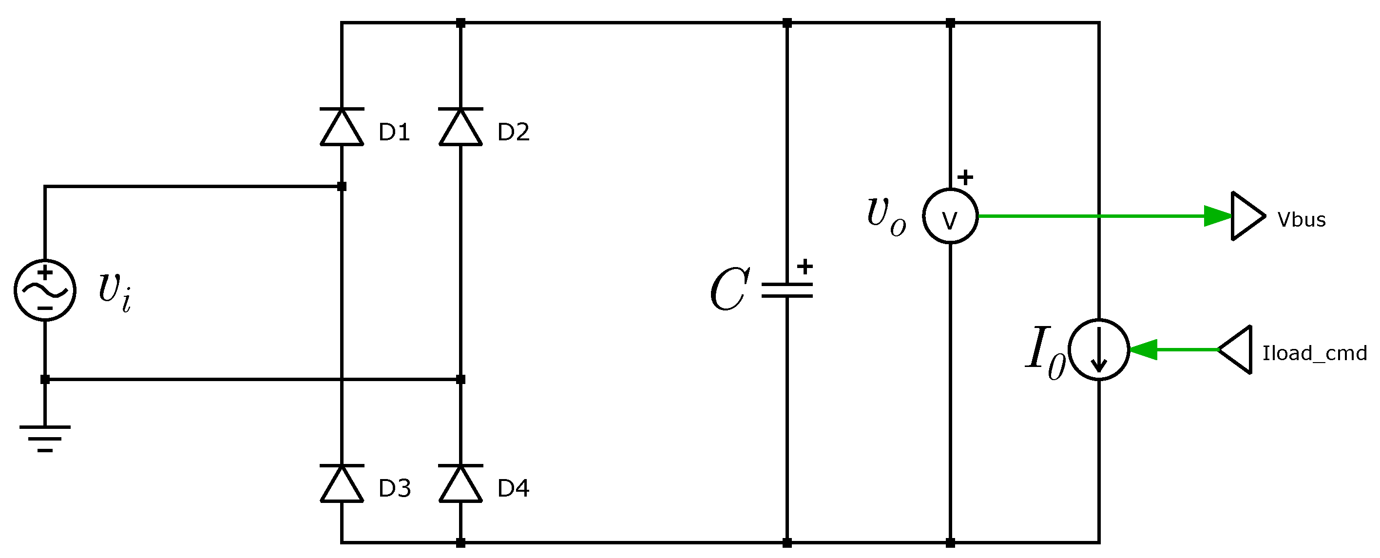
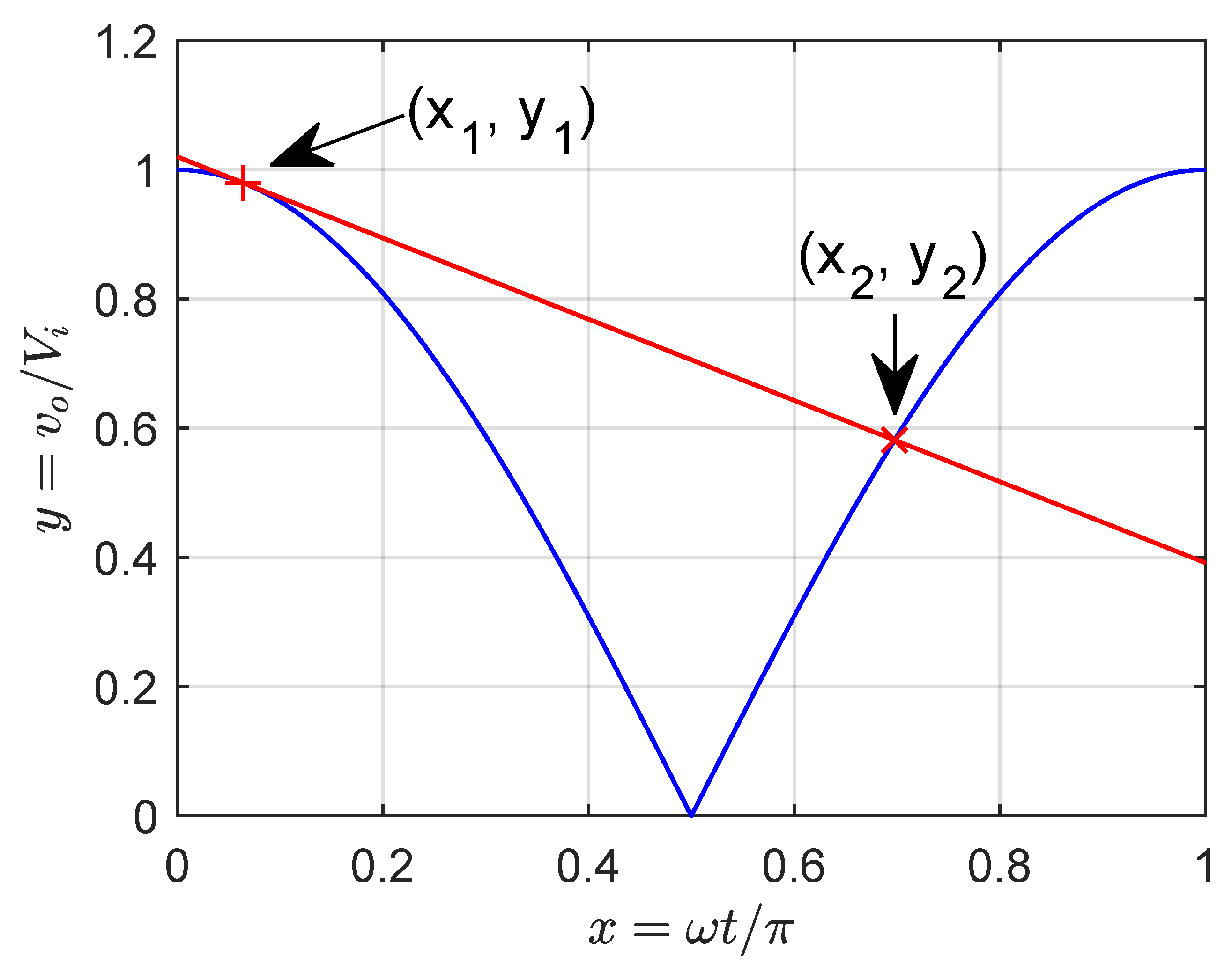
2.1. Uncontrolled Rectifier and Its Limitations

In this first part of the study, the simple uncontrolled rectifier of Figure 1 is studied to find the relationship between the load and the required capacitance. We study this system because the resulting relationship is the same for the sizing of the boost PFC converter that will, in turn, share the same issues. PF computation is outside the scope of the present discussion, and it will be covered thoroughly in Section 2.3.
For this study, the rectified waveform is analyzed as shown in Figure 2. Here, a sinusoid v i ( t ) = V i cos ( ω t ) with amplitude V i and angular frequency ω is assumed as the input to the rectifier, and v o is the output of the circuit. In Figure 1, C is the capacitance to be designed and the load is assumed to be a constant current load I 0 : this is not exactly correct for current-controlled drives, which behave more as a constant power load; a more accurate model is given in the numerical simulations of Section 2.3.
The normalized variables of Figure 2 are y = v o / V i and x = ω t / π . The load current is supplied by the capacitor when all the diodes are off. This happens for
C d v o d t = I 0
Because of the shape of v o , there is a lower bound on the capacitance value, which guarantees that (1) is satisfied for a normalized time x < 1 / 2 :
C > C min = I 0 ω V i
We subsequently use this normalization constant in the following: c = C / C min . If (2) holds, then it is possible to determine x 1 , the point where the diodes stop conducting, as
x 1 = 1 π arcsin 1 c 1 π c
We can then compute the value at which the capacitor starts discharging:
y 1 = cos π x 1 = 1 1 c 2 1 1 c 2
In both the formulas above, the approximations hold for c 1 , which is usually a practical design condition. By considering the capacitor discharge, we find the moment x 2 at which the diodes turn on again by solving:
π c ( x 2 x 1 ) y 1 = cos ( π x 2 )
which is a transcendental equation and requires numerical solving. We can still give a quite accurate estimation by using the first-order Taylor expression for the cosine around x = 3 / 4 , which is halfway in the range where the solution x 2 is expected to fall:
x 2 2 / c + 2 c 2 1 + c ( 3 π / 4 1 ) π ( c + 2 ) e c π ( c + 2 )
where e is the Nepero constant, which appears as an unexpected approximation of the numerator coefficient in (6). We can then find the value y 2 and, subsequently, the voltage peak-to-peak ripple y ˜ and the average voltage y ¯ at the output of the rectifier:
y 2 = y 1 π c ( x 2 x 1 ) 1 e c + 2
y ˜ = 1 y 2 e c + 2
y ¯ = 1 + y 2 2 c c + 2
Equations (8) and (9) clearly show that the higher c is the best, yet there is an asymptotic behavior that discourages the use of very high values of C. Nonetheless, the application will pose constraints on y ˜ and y ¯ , so these will be used for sizing C. Figure 3 reports all the aforementioned quantities in normalized units, with both the numerical results and the given approximations. It can be seen that the average output voltage in the case of C < C min is 2 / π , as it results from straightforward averaging of the rectified cosine.

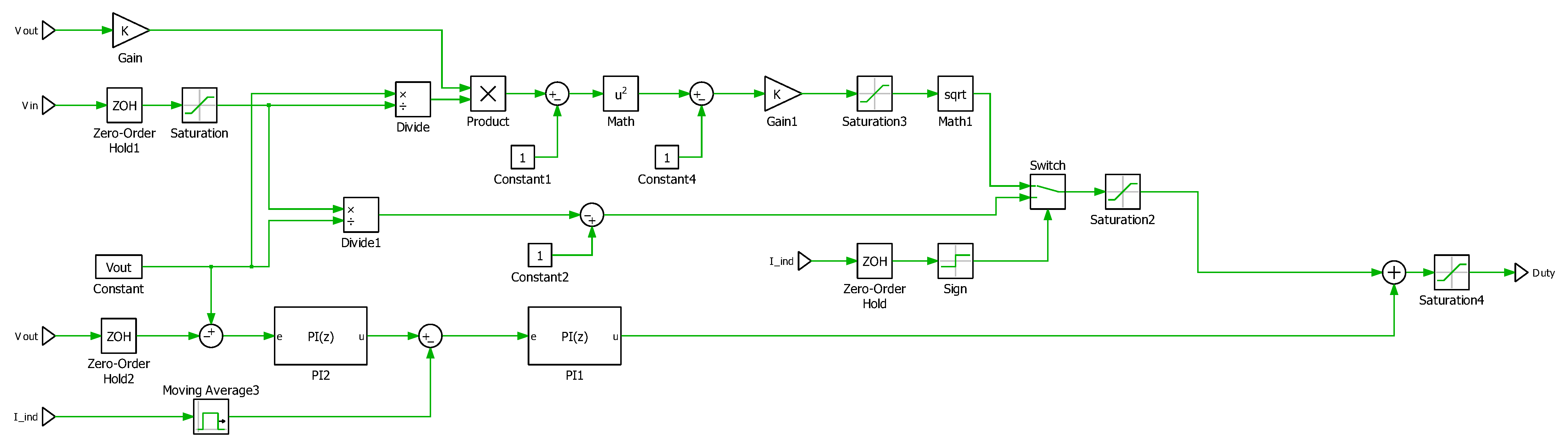
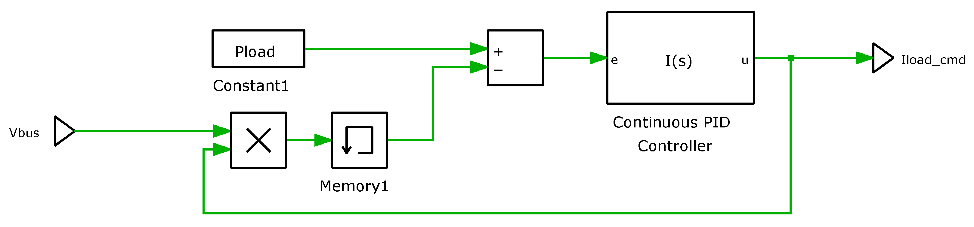
2.2. Proposed Control for DC Link Capacitance Reduction

PFC is a primary practice for AC-DC converters in order to fulfill the requirements of international standards. PFC will reduce THD in the supply current and boost the efficiency of the system. Although numerous methods have been suggested to improve power factor, the novel control method proposed in this article, shown in Figure 4 and the corresponding schematic in Figure 5e, is based on a boost PFC circuit presented in [15], with the schematic shown in Figure 5d.
This control method has two fundamental aims: decrease the front end capacitor to achieve an electrolytic capacitor-less circuit and, at the same time, keep the high PF. To do so, a new control method has been built based on the summation of two distinct duty cycle components:
1.
Feed-forward control [24,25]: Boost converter can work in two distinct modes, continuous conduction mode (CCM) and discontinuous conduction mode (DCM), depending on whether the inductor current reaches zero during the switching period. The duty cycle definition is different in the two modes once input and output voltage are chosen:
d C C M = 1 V i n V o u t
d D C M = L 2 R o u t T s w V o u t I o u t V i n 1 2 1
CCM control methods are more commonly used given their simplicity; however, in variable load applications, DCM may occur, changing the duty cycle relationship.
2.
Feed-back control [26,27]: a dual nested loop linear feedback control is implemented for parameter adaptation and to improve load and line regulation. The inner current loop generates the duty cycle to control (and limit) the inductor current; the outer voltage loop generates a current setpoint to regulate the voltage of the DC link to the desired value, while minimizing the ripple.

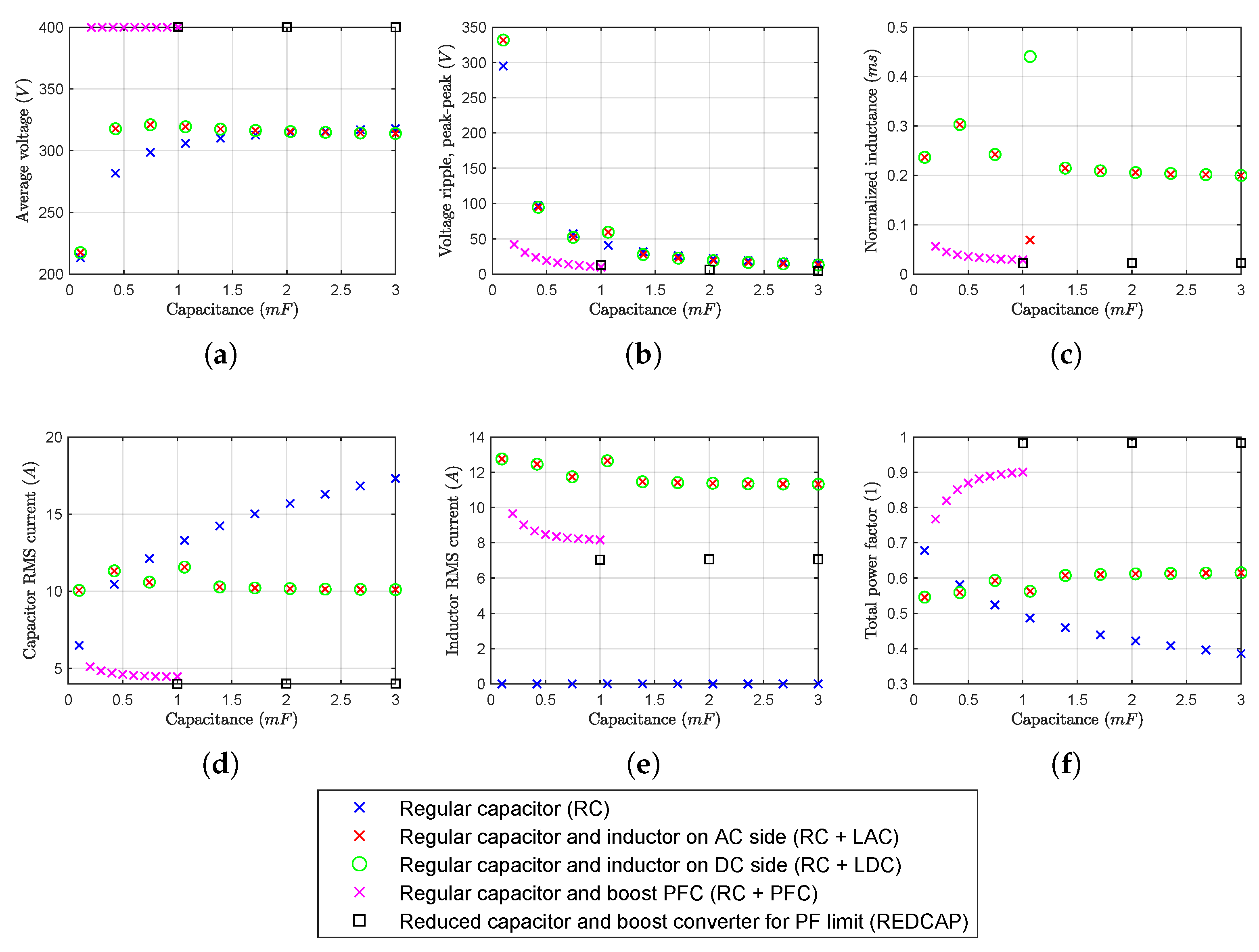
2.3. Comparison of Different Rectifier Topologies

To maximize the benefits of the control described in Section 2.2 and to properly choose the most appropriate rectifier front-end depending on the specific application, five different rectifier topologies are compared by simulation in this section:
1.
Regular capacitor (RC);
2.
Regular capacitor and inductor on DC side (RC + LDC);
3.
Regular capacitor and inductor on AC side (RC + LAC);
4.
Regular capacitor and boost PFC (RC + PFC);
5.
Reduced capacitor and boost converter for PF limit (REDCAP).
The acronyms in parentheses are used for later reference in the discussion, and the schematics of each topology are given in Figure 5.
These topologies are compared according to several metrics. From the functional point of view, DC voltage average value and peak-to-peak ripple are evaluated, as well as the power factor. Particularly, the latter is split into three components, one of which is phase-shift related and two of which are related to the distortion of both current and voltage. When an AC voltage v ( t ) is applied to a non-linear load (such as the rectifier bridge), the current i ( t ) may contain relevant harmonic components. We can express both quantities in terms of Fourier series:
v ( t ) = V 0 2 + n = 1 V n cos n ω t + φ v n
i ( t ) = I 0 2 + n = 1 I n cos n ω t + φ i n
The active power P can thus be computed by its definition, as the average of the instantaneous power p ( t ) :
P = 1 T T p ( t ) d t = 1 T T v ( t ) i ( t ) d t = = V 0 I 0 + V 1 I 1 2 cos φ v 1 φ i 1 + n = 2 V n I n 2 cos φ v n φ i n
where the first term is the DC power, which is supposed to be zero, the second term is the fundamental frequency power (the desired one), and the last term is the higher-harmonics related power (which is undesirable and cannot be exploited practically in most applications). Considering that for any signal x ( t ) we can express its RMS and THD values, respectively, as
X r m s 2 = 1 T T x 2 ( t ) d t = X 0 2 + n = 1 X n 2 2 = X 0 2 + X 1 , r m s 2 + n = 2 X n , r m s 2
THD x = 1 X 1 n = 2 X n 2 = 1 X 1 , r m s n = 2 X n , r m s 2 = X r m s 2 X 1 , r m s 2 1
where X n , r m s = X n / 2 are the RMS values of the harmonics. We can now express the active power as a function of RMS values, phase-related power factor PF φ = cos ( φ v 1 φ i 1 ) , and the two distortion-related power factors PF D v and PF D i
P = V r m s I r m s PF φ 1 1 + THD v 2 1 1 + THD i 2 = = V r m s I r m s PF φ PF D v PF D i = V r m s I r m s PF
In the simulations used here, we assume THD v = 1 , i.e., PF D v = 1 , assuming that the AC source has a very low impedance and is insensitive to current distortion; this is somehow a best case, but it still gives a fair comparison of the various topologies.
To ensure fairness with respect to the drive application the grid front-end is supposed to work with, all the circuits are evaluated at the same output power. This is slightly different from the usual constant current model of the load (see an example in Section 2.1), but it best describes the load presented by the torque- and speed-controlled drive, which will require more current in case of lower DC voltage, provided that there is still some voltage margin. This descends from the fact that a torque set-point at any given speed gives an output mechanical power, hence a similar power (increased by the motor inverter loss) will be requested to the upfront converter. To model this type of load, a linear, integrator-based control is introduced. Figure 6 shows the control, where V bus is the DC link voltage and I load , cmd is the command of the dependent current generator acting as load at each rectifier output.
In addition to these functional parameters, the circuits are also evaluated with respect to some relevant implementation parameters: size of inductor, capacitor and inductor RMS current, and total power factor (combining phase displacement and distortion on the current). The size of the inductor is obtained by computing the maximum stored energy and normalizing it with respect to the (constant) power load (as done in [28]), thus giving an effective “time of load supply”. This enables understanding of how the energy is stored in the various components and justifies that this quantity is expressed in time units (milliseconds), which results by dividing energy by power.
The aforementioned indexes are given in Figure 7. The magenta points, representing the reduced capacitor rectifier, are computed on a narrower capacitance range, as this rectifier is supposed to be used with small capacitance values. According to the boost nature of the front-end, the output voltage is controlled (in this case) at 400 V , with a very small ripple (<10%) also for capacitor values of 200 μ F , for a 1.6   k W load power. Concerning the average output voltage, described in Figure 7a, the boost topologies are only capable of controlling the DC voltage actively, whereas the uncontrolled ones depend heavily on the capacitance value and reach an asymptotic limit at 325 V , corresponding to the peak of the sinusoid. Similar considerations apply to the voltage ripple in Figure 7b: it is lower for controlled topologies, asymptotic to zero for very high capacitance values, and equal to the sinusoid peak for capacitance values lower than C m i n . It is interesting to see (Figure 7c) that, even if the inductance has the same value as in uncontrolled designs, the normalized size of this component is smaller, due to the lower RMS current.
Figure 7d,e report the RMS current on capacitor and inductor (if present), respectively. In that case, the capacitor RMS current, main driver for lifetime, for controlled topologies is half of the uncontrolled ones with an inductor and roughly one-third of the rectifier with capacitor alone. Figure 7f shows an interesting feature of the presented control: even if the overall PF is not addressed directly by the control, the performance of the converter under this aspect is absolutely remarkable. However, unity power factor cannot be reached, as the curve appears to reach an asymptote around 0.9 .
The “traditional” boost PFC has similar performance to the proposed circuit, when properly sized, it achieves almost unity power factor; however it cannot operate in the full capacitance range, as its control is based on the hypothesis of a virtual resistive output load, which fails with low capacitance [15]. The small discrepancy in PF in this case is related to the residual THD of the current (connected to the inductor current ripple): the phase related component is, however, exactly unity.
Finally, it can be noted that, when using a passive topology with an inductor, putting it on the AC or DC side does not affect the performance, as it may be arguable by the behavior of an ideal rectifier.

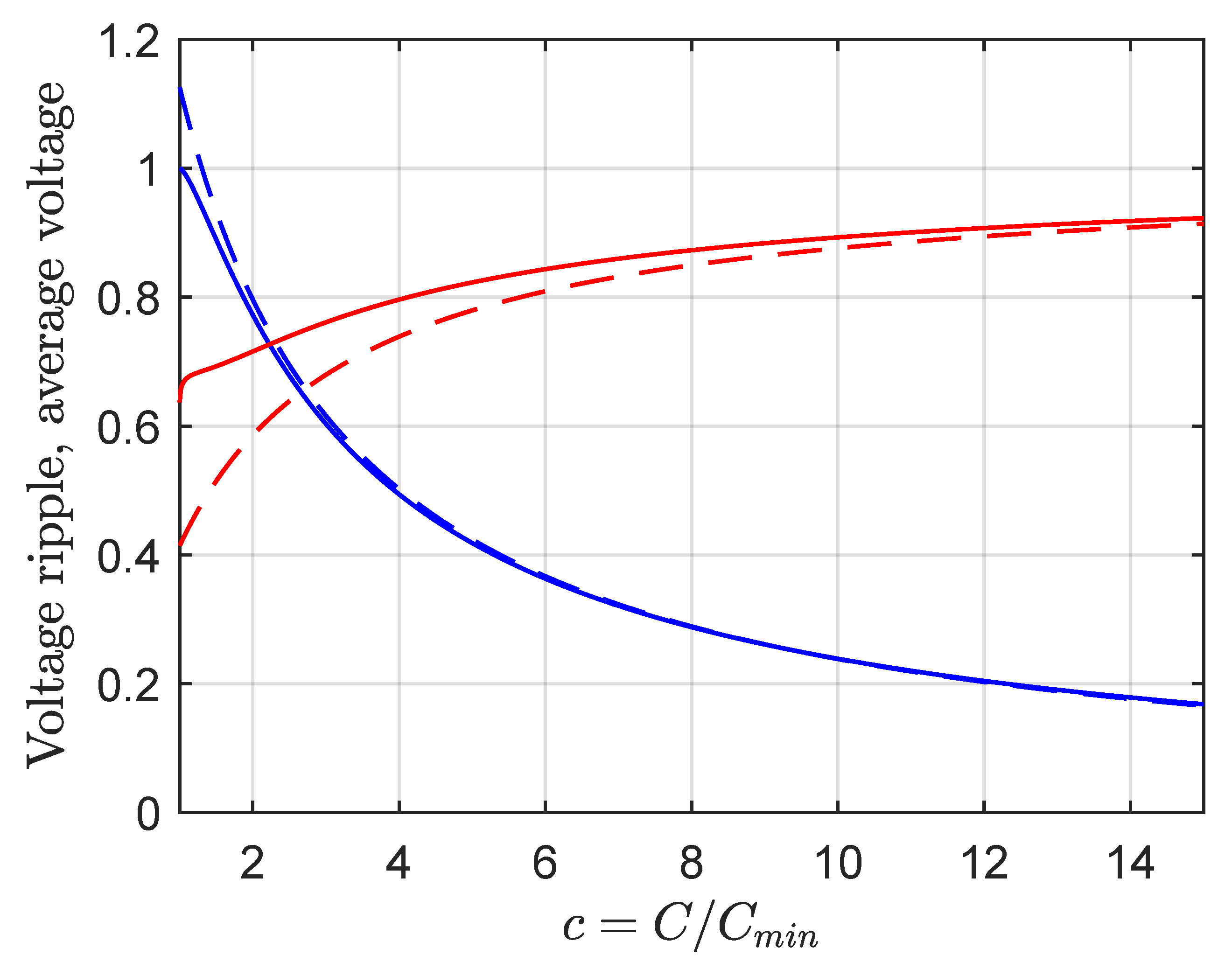
2.4. Control Design Tradeoff
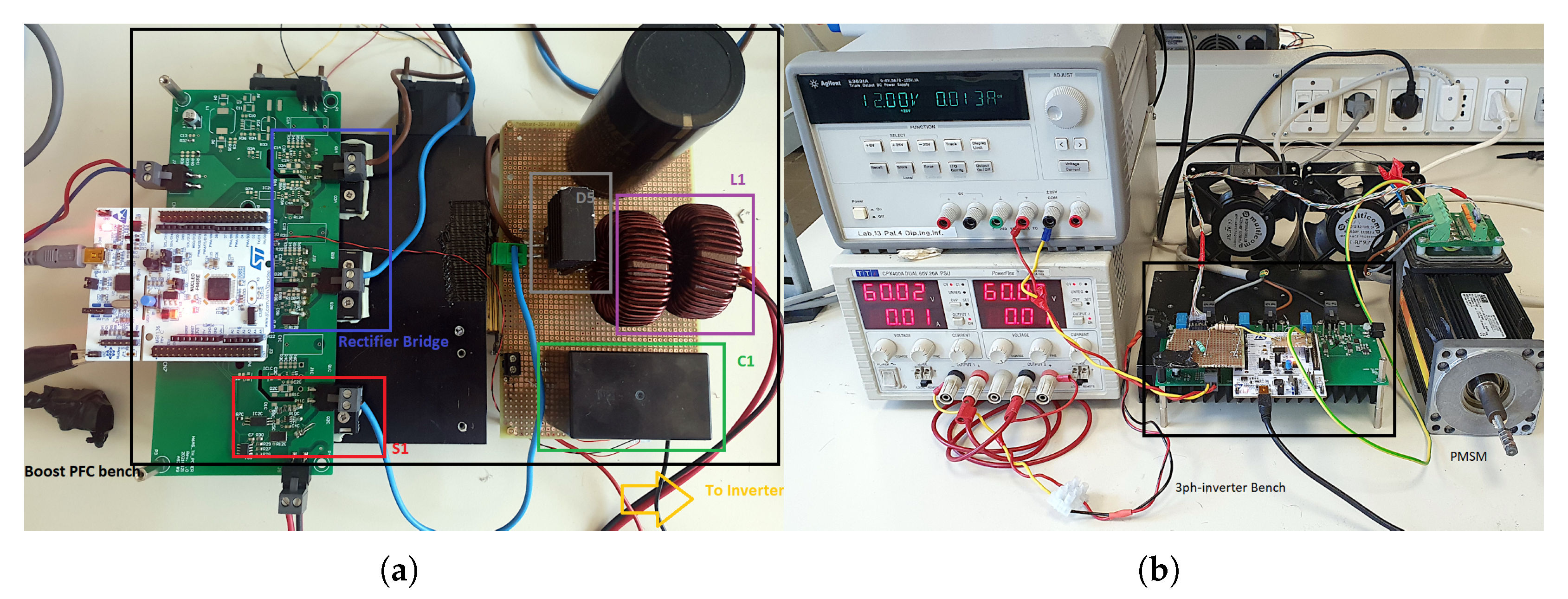
The most noteworthy design choice in this control architecture is based on the trade-off between ripple output voltage, inductor RMS current, and PF, depending on the PI tuning. Different results can be achieved with the possibility of optimizing one parameter to the detriment of the others, resulting in a critical challenge in PFC design. Table 1 shows the boost PFC parameters used in simulation to compare the performance of the proposed controller with three different tuning PI gains noted in Table 2, where PI1 (P1, I1) are related to inner current loop and PI2 (P2, I2) refers to outer voltage loop, as shown in Figure 4. According to Table 2, with fixed proportional and integral gain of the inner loop and fixed integral gain of the outer loop, if we decrease the proportional gain of the outer loop, the inductor RMS current will decrease, improving the power factor, and this will negatively impact the output voltage ripple. In contrast, with fixed proportional and intergral gain of the outer loop and fixed proportional gain of the inner loop, if we increase the integral gain of the inner loop, it is possible to reach high PF at the cost of very high output voltage ripple. These results show that inductor RMS current, voltage ripple, and total PF are sensitive to the change in controller gain.
The switching frequency is another important design aspect, and some circuit elements behavior (e.g., power dissipation on the switch) depends on this parameter. For that reason, the switching frequency could be a design constraint. The most frequency dependent values in boost converters are the inductor RMS current and the output voltage ripple; however, the proposed control reduces this dependency, imposing current and voltage behavior and proper saturation. In the case of low switching frequency, the boost PFC will work in DCM while it is not an issue for the proposed control, which is able to detect the mode change and adapt in the proper way.

3. Results

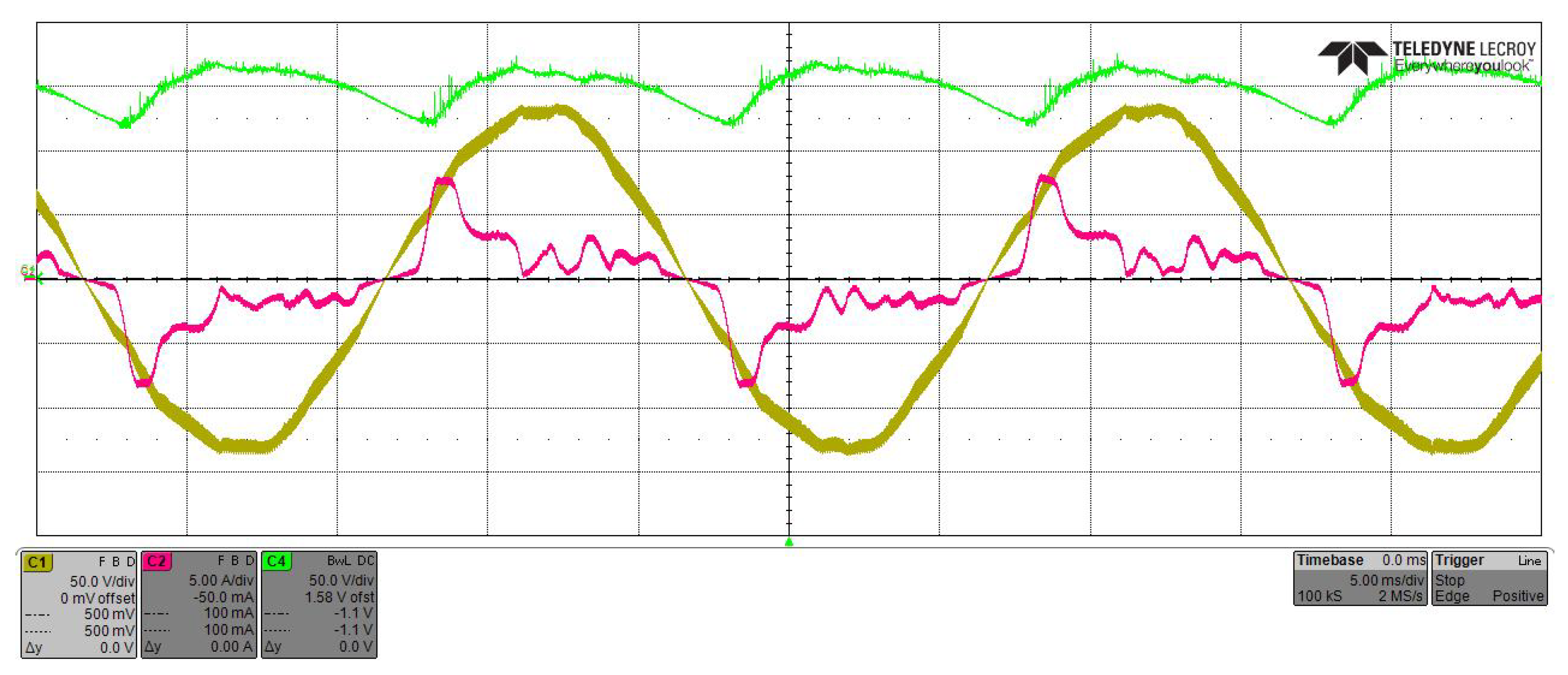
3.1. Boost Front-End with Film Capacitor

The boost converter with reduced DC link capacitance is first tested in a standalone fashion, with a purely resistive load, as shown in Figure 5e. Figure 8a represents the test bench used to gather the results. The boost front-end parameters are summarized in Table 3.
The validation test has been made using the parameters summarized in Table 3. As shown in Figure 9, the boost PFC converter with reduced DC link capacitance works as expected, achieving a high PF ( > 0.75 , depending on control parameters), comparable to the simulations shown in Figure 7f with low capacitance. The output voltage ripple is high (≈ 45 V ) but still compatible to the simulations results in Figure 7b with low capacitance.
Once the proposed DC link voltage control is validated on its own, it is coupled with a conventional, resolver-based three-phase drive for PMSM, as shown in Figure 10; the drive test bench is represented in Figure 8b. The drive parameters are given in Table 4.

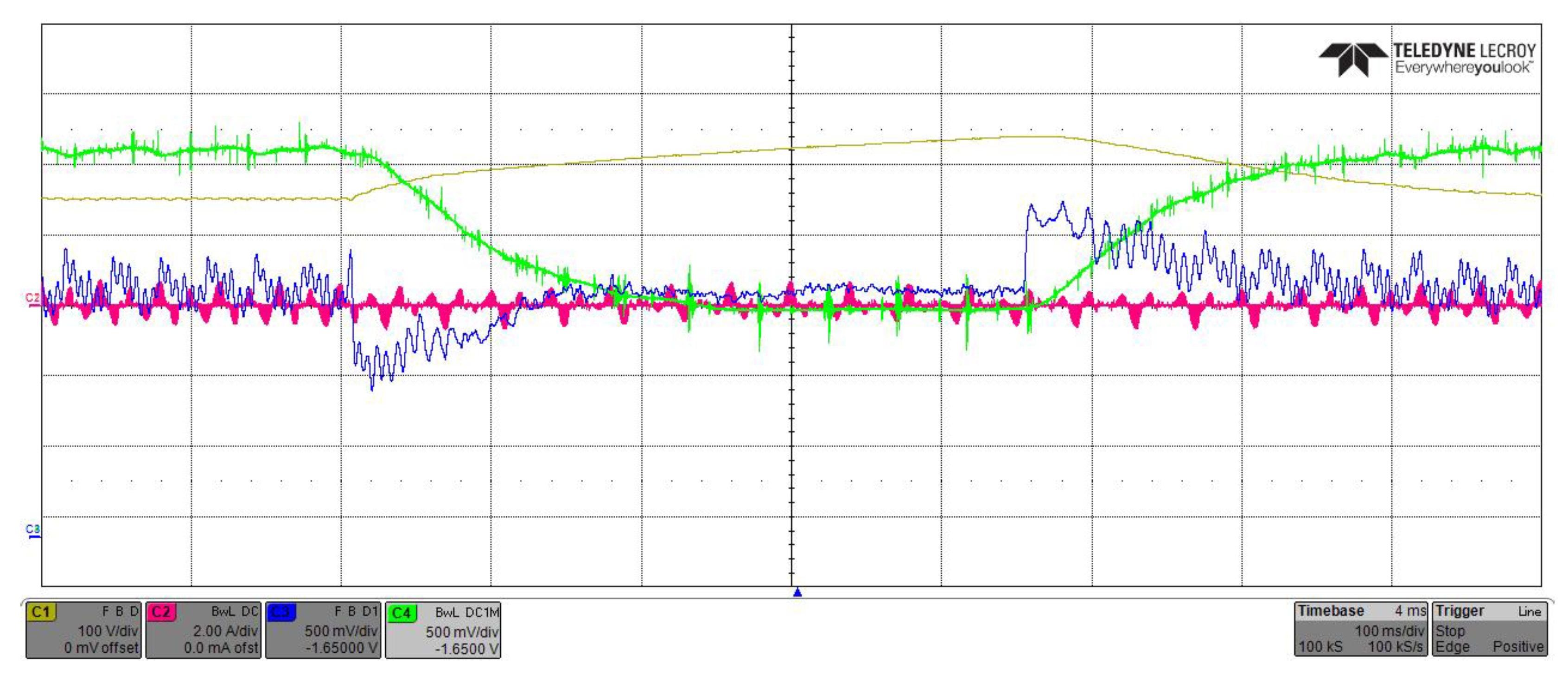
3.2. System Performance in Regenerative Conditions

To analyze the regenerative braking process, the proposed PFC boost converter front-end is coupled with a full bridge inverter PMSM controller. According to Figure 11, the motor is spinning at 100 rad   s 1 , and the voltage of the DC link is set to 150   V . At a certain time, a braking signal is applied to the rotor to reach zero speed and stop. During deceleration in the regenerative braking period, negative q-axis current is being generated, flowing into the DC link capacitor and charging it up to 90   V . After almost 500   m s , reference speed has been changed into 100 rad   s 1 again, so the motor begin accelerating to reach steady state in almost 250   m s . Based on practical results shown in Figure 11, during the charge and discharge time, the DC link voltage ripple has been controlled with appropriate performance.

4. Conclusions

In this paper, a new methodology has been proposed to control DC link voltage ripple using usual boost front-end employed for PFC, based on two separate duty cycle components generating the switching command signal. This approach allowed us to reduce the capacitance and consequently use a Long-life low ESR film capacitor instead of a bulky electrolytic type, leading to improved performance in terms of reliability. Five different rectifier topologies were compared in simulation to observe the performance of the method at the same output power. The simulation and experimental results confirm the performance of the proposed approach from the functional point of view; DC voltage average, peak-to-peak ripple, and power factor also with respect to some relevant implementation parameters: size of inductor, capacitor, and inductor RMS current and total power factor. Finally, the proposed DC link voltage control has been coupled with a conventional, resolver-based three-phase drive for PMSM to see the DC link situation in the presence of the regenerative braking. Experimental results show the appropriate performance of the proposed DC link controller during the charge and discharge of the DC link capacitor. As a part of prospective work, the DC link voltage control should also include the management of an active braking resistor to control the discharge part of the regenerative braking process while enlarging the range of safe regenerated power.

Author Contributions

Conceptualization, A.S.; methodology, A.S.; software, A.M. and H.S.L.; validation, A.M., H.S.L., and A.S.; formal analysis, A.S.; investigation, A.M., H.S.L., and A.S.; resources, A.S.; data curation, A.M. and H.S.L.; writing—original draft preparation, A.S.; writing—review and editing, A.M. and H.S.L.; visualization, A.M. and H.S.L.; supervision, A.S.; project administration, A.S.; funding acquisition, A.S. All authors have read and agreed to the published version of the manuscript.

Funding

This research has financially been supported by the Programme “FIL-Quota Incentivante” of University of Parma and co-sponsored by Fondazione Cariparma. The APC was funded by the Programme.

Institutional Review Board Statement

Not applicable.

Informed Consent Statement

Not applicable.

Data Availability Statement

Not applicable.

Acknowledgments

The authors wish to thank Plexim GmbH, Zurich, Switzerland for supporting this work by licensing their PLECSTM simulator, which was used for the automated performance evaluation of the various rectifier topologies and rapid control prototyping.

Conflicts of Interest

The authors declare no conflict of interest. The funders had no role in the design of the study; in the collection, analyses, or interpretation of data; in the writing of the manuscript, or in the decision to publish the results.

Abbreviations

The following abbreviations are used in this manuscript:
CCMContinuous Conduction Mode
DCMDiscontinuous Conduction Mode
ESREquivalent Series Resistance
LLLine-to-Line
PECPower Electronics Converter
PFPower Factor
PFCPower Factor Correction
RMSRoot Mean Square
THDTotal Harmonic Distortion

References

  1. Åhag, P.; Hed, L.; Lundow, P.H.; Olsson, L. Are We Ready for the Agenda 2030 for Sustainable Development? In Proceedings of the 2019 IEEE International Conference on Industrial Engineering and Engineering Management (IEEM), Macao, China, 15–18 December 2019; pp. 224–227. [Google Scholar] [CrossRef]
  2. United Nations General Assembly. Transforming Our World: The 2030 Agenda for Sustainable Development. 2015. Available online: https://unric.org/en/sdgs-in-your-language/ (accessed on 19 July 2022).
  3. Samad, H.A.; Zhang, F. Benefits of Electrification and the Role of Reliability: Evidence from India; Policy Research Working Paper Series 7889; The World Bank: Washington, DC, USA, 2016. [Google Scholar] [CrossRef]
  4. Hasanbeigi, A. Industrial Heating Profile and Electrification. 2021. Available online: https://www.globalefficiencyintel.com/new-blog/2021/3/22/industrial-heating-profile-and-electrification (accessed on 19 July 2022).
  5. Stoffel, B. Chapter 1—The Role of Pumps for Energy Consumption and Energy Saving. In Assessing the Energy Efficiency of Pumps and Pump Units; Stoffel, B., Ed.; Elsevier: Boston, MA, USA, 2015; pp. 1–24. [Google Scholar] [CrossRef]
  6. Hasanbeigi, A. Infographic: The Profile of Energy Use in Industrial Motor Systems. 2017. Available online: https://www.globalefficiencyintel.com/new-blog/2017/infographic-energy-industrial-motor-systems (accessed on 19 July 2022).
  7. Waide, P.; Brunner, C.U. Energy Efficiency Policy Opportunities for Electric Motor-Driven Systems; Technical report; International Energy Agency: Paris, France, 2011.
  8. Tanaka, T. Environment friendly revolution in home appliances. In Proceedings of the 13th International Symposium on Power Semiconductor Devices & ICs. IPSD ’01 (IEEE Cat. No.01CH37216), Osaka, Japan, 7 June 2001; pp. 91–95. [Google Scholar] [CrossRef]
  9. Williams, M. The Role of Power Semiconductors in Enhancing Home Appliance Efficiency. 2021. Available online: https://www.embedded.com/the-role-of-power-semiconductors-in-enhancing-home-appliance-efficiency/ (accessed on 19 July 2022).
  10. Xia, Y.; Fletcher, J.; Finney, S.; Ahmed, K.; Williams, B. Torque ripple analysis and reduction for wind energy conversion systems using uncontrolled rectifier and boost converter. IET Renew. Power Gener. 2011, 5, 377–386. [Google Scholar] [CrossRef]
  11. Kolli, N.; Pramod, P.; Bhattacharya, S. Analysis of Different Operating Modes of PMSM during Regeneration with Uncontrolled Rectifier. In Proceedings of the 2020 IEEE Transportation Electrification Conference & Expo (ITEC), Chicago, IL, USA, 23–26 June 2020; pp. 204–209. [Google Scholar] [CrossRef]
  12. Turchi, J.; Dalal, D.; Wang, P.; Jenck, L. Power Factor Correction (PFC) Handbook; HBD853/D; ON Semiconductor: Denver, CO, USA, 2014. [Google Scholar]
  13. Rossetto, L.; Spiazzi, G.; Tenti, P. Control Techniques for Power Factor Correction Converters. In Proceedings of the International Conference on Power Electronics and Motion Control, Warsaw, Poland, 20–22 September 1994; pp. 1310–1318. [Google Scholar]
  14. De Souza, A.F.; Pereira, D.C.; Tofoli, F.L. Comparison of control techniques used in power factor correction rectifiers. In Proceedings of the 2015 IEEE 13th Brazilian Power Electronics Conference and 1st Southern Power Electronics Conference (COBEP/SPEC), Fortaleza, Brazil, 29 November–2 December 2015; pp. 1–6. [Google Scholar] [CrossRef]
  15. Kim, J.; Choi, H.; Won, C.Y. New Modulated Carrier Controlled PFC Boost Converter. IEEE Trans. Power Electron. 2018, 33, 4772–4782. [Google Scholar] [CrossRef]
  16. Zhou, Y.; Huang, W.; Hong, F. Single-Phase Input Variable-Speed AC Motor System Based on an Electrolytic Capacitor-Less Single-Stage Boost Three-Phase Inverter. IEEE Trans. Power Electron. 2016, 31, 7043–7052. [Google Scholar] [CrossRef]
  17. Ramos-Paja, C.A.; Saavedra-Montes, A.J.; Bastidas-Rodriguez, J.D. Co-Design of the Control and Power Stages of a Boost-Based Rectifier with Power Factor Correction Depending on Performance Criteria. Computation 2022, 10, 61. [Google Scholar] [CrossRef]
  18. Rossetto, L.; Spiazzi, G.; Tenti, P. Boost PFC with 100 Hz switching frequency providing output voltage stabilization and compliance with EMC standards. In Proceedings of the Conference Record of 1998 IEEE Industry Applications Conference, Thirty-Third IAS Annual Meeting (Cat. No.98CH36242), St. Louis, MO, USA, 12–15 October 1998; Volume 2, pp. 1567–1573. [Google Scholar] [CrossRef]
  19. Albertsen, A. Electrolytic Capacitor Lifetime Estimation. Bodos Power Magazine, 1 April 2010. [Google Scholar]
  20. Reliability of Aluminum Electrolytic Capacitors. Technical Report; ELNA America Inc.: Marietta, GA, USA, 2022.
  21. Lifetime of Aluminum Electrolytic Capacitors. Available online: https://www.chemi-con.co.jp/en/faq/detail.php?id=29BDBH5 (accessed on 19 July 2022).
  22. Wang, H.; Blaabjerg, F. Power Electronics Reliability: State of the Art and Outlook. IEEE J. Emerg. Sel. Top. Power Electron. 2021, 9, 6476–6493. [Google Scholar] [CrossRef]
  23. Manohar, S.S.; Sahoo, A.; Subramaniam, A.; Panda, S.K. Condition monitoring of power electronic converters in power plants—A review. In Proceedings of the 2017 20th International Conference on Electrical Machines and Systems (ICEMS), Sydney, NSW, Australia, 11–14 August 2017; pp. 1–5. [Google Scholar] [CrossRef]
  24. Wu, S.T.; Chen, F.Y.; Chien, M.C.; Wang, J.M.; Su, Y.Y. A Hybrid Control Scheme with Fast Transient and Low Harmonic for Boost PFC Converter. Electronics 2021, 10, 1848. [Google Scholar] [CrossRef]
  25. Chen, M.; Sun, J. Feedforward current control of boost single-phase PFC converters. IEEE Trans. Power Electron. 2006, 21, 338–345. [Google Scholar] [CrossRef]
  26. Gupta, A.; Panwar, A.; Sahoo, S.K.; Jacob Raglend, I. A CCM/DCM Hybrid Control Scheme for Single Channel Boost PFC Converter to Improve Power Quality. In Proceedings of the 2019 Innovations in Power and Advanced Computing Technologies (i-PACT), Vellore, India, 22–23 March 2019; Volume 1, pp. 1–5. [Google Scholar] [CrossRef]
  27. Moldaschl, J.; Broulím, J.; Paločko, L. Boost power factor correction topology with average current control. In Proceedings of the 2014 International Conference on Applied Electronics, Pilsen, Czech Republic, 9–10 September 2014; pp. 213–216. [Google Scholar] [CrossRef]
  28. Tripathi, P.R.; Thakura, P.; Keshri, R.K.; Ghosh, S.; Guerrero, J.M. Twenty-Five Years of Single-Stage Buck–Boost Inverters: Development and Challenges. IEEE Ind. Electron. Mag. 2022, 16, 4–10. [Google Scholar] [CrossRef]
Figure 1. Schematic of the uncontrolled rectifier without an inductor used for the simplified computation of the capacitance requirements.
Energies 15 05929 g001
Figure 2. Normalized waveforms of the uncontrolled rectifier used for the analysis of the capacitance requirements.
Energies 15 05929 g002
Figure 3. Normalized design quantities for the capacitor-only rectifier. Exact results based on numerical solution are solid, whereas dashed lines pertain to the approximations used for the design described above.
Energies 15 05929 g003
Figure 4. Schematic of the control algorithm for the boost front-end with capacitor-reduction action. Three control branches can be recognized: feed-forward for CCM, feed-forward for DCM, and linear feedback control with inner inductor current loop and outer voltage loop; V i n is the input voltage after the rectifier, V o u t is the DC output voltage, and I i n d is the inductor current.
Energies 15 05929 g004
Figure 5. The schematics of the five topologies compared in the simulation study. RC + PFC and REDCAP are basically identical; only their control algorithm changes.
Energies 15 05929 g005
Figure 6. The simple control used to compare all the simulations with constant power output, regardless of the effective DC link voltage achieved by each uncontrolled topology.
Energies 15 05929 g006
Figure 7. Simulation comparison of the most relevant performance indexes for the five rectifier topologies considered: (a) average output voltage, (b) output voltage ripple, (c) normalized inductance value, (d) capacitor RMS current, (e) inductor RMS current, (f) overall power factor (phase and harmonics). The inductance value is 600 μ H and the output power is 1.6 k W .
Energies 15 05929 g007
Figure 8. The two test benches used to test the electrolytic capacitor-less drive: (a) the rectifier stage, (b) the three-phase motor drive stage.
Energies 15 05929 g008
Figure 9. Capacitor-less PFC test conducted using the parameters summarized in Table 3: input voltage (yellow), input current (magenta), output voltage (green).
Energies 15 05929 g009
Figure 10. Schematic of the boost PFC converter coupled with full bridge inverter drive.
Energies 15 05929 g010
Figure 11. Regenerative braking test: input DC voltage of inverter (yellow), input current of the boost PFC (magenta), q-axis current of the motor from DAC scaled to 0.15 A per division on the oscilloscope with 1.65 V offset to show negative and positive current (blue), motor speed scaled to 55 rad   s 1 per division on the oscilloscope with 1.65 V offset to show negative and positive speed (green).
Energies 15 05929 g011
Table 1. The parameters of the boost converter used in simulation for the evaluation of the control performance and sensitivity to controller tuning.
ParameterSymbolValue
Input voltage (peak) v i 325   V
Input frequency f 0 50   Hz
Switching frequency f s w 25   kHz
Output voltage v o 400   V
InductanceL 610   μ H
CapacitanceC 110   μ F
Resistive load R o 100   Ω
Table 2. Proposed control performance under three different sets of parameters for PI controller tuning.
ParameterTuning 1Tuning 2Tuning 3
P 1 20 × 10 3 20 × 10 3 20 × 10 3
I 18080300
P 2 180 × 10 3 10 × 10 3 10 × 10 3
I 2202020
Inductor current (RMS) 10.9   A 7.8   A 7.6   A
Output voltage ripple (peak-peak) 45   V 86   V 103   V
Total power factor 0.75 0.85 0.91
Table 3. The boost converter parameters.
ParameterSymbolValue
Input voltage (peak) v i 125   V
Input frequency f 0 50   Hz
Switching frequency f s w 25   kHz
Output voltage v o 150   V
InductanceL 610   μ H
CapacitanceC 110   μ F
Resistive load R o 100   Ω
Table 4. The drive parameters.
ParameterSymbolValue
Motor rated torque T n 2.2   N m
Motor rated speed ω n 1000   rpm
Motor rated power P n 230   W
Motor rated current (phase, RMS) I n 2.42   A
Motor rated voltage (LL, RMS) V n 380   V
Publisher’s Note: MDPI stays neutral with regard to jurisdictional claims in published maps and institutional affiliations.

