Abstract
The instantaneous output power of the two-stage inverter pulsates at twice the output frequency, resulting in the second harmonic current (SHC) in the front-end dc-dc converter. To reduce the SHC in the inductance branch while maintaining good dynamic performance, this paper proposes a control scheme based on a new inductor current feedback path in the front-end buck converter. In the scheme, through the equivalent gain, the virtual resistor, and the bandpass filter, the inductor current is fed to the front of the voltage regulator. The feedback function simplification is studied and the implementation of the proposed scheme is illustrated. With considerations of both reducing the SHC and improving the dynamic performance, the parameter design approach for the feedback function is also presented for the proposed SHC reduction control scheme, and the performance analysis and comparison from the viewpoint of output impedance are provided. The simulation model and the prototype of a 10 kW two-stage inverter are constructed. The simulation and experimental results about the low SHC in the front-end buck converter and the fast dynamic response during the load transient verify the effectiveness of the proposed scheme.
1. Introduction
The two-stage inverter is composed of a front-end dc-dc converter and a downstream single-phase inverter, which is widely used for the power supply with a wide input voltage range [1,2,3,4]. The instantaneous output power of the single-phase inverter fluctuates at twice the output frequency (2fo), resulting in the second harmonic current (SHC) in the inductance branch of the front-end dc-dc converter [5,6]. The SHC will increase the current stress and power losses of the power switches and the magnetic components, decrease the energy conversion efficiency, and shorten the lifespan of the dc source such as fuel cells and batteries [7,8,9]. Thus, it is necessary to reduce the SHC in the dc-dc converter.
The SHC reduction approaches can be classified into two categories. The first approach is to provide the additional hardware circuit for the two-stage inverter. In [10], an improved circuit consists of an isolated dc/dc converter and interconnection inverter, which achieves the dc active filter function and reduces the ripple current to approximately 20% of that of the conventional circuit. An active low-frequency ripple control device based on the virtual capacitor concept is proposed [11], and the low-frequency ripple current caused by the single-phase inverter can be compensated by introducing a current integrator. Moreover, an SHC compensator (SHCC) is adopted to buffer the ripple power in a single-phase power factor correction converter and a single-phase inverter [12,13], and the SHCC is connected to the dc bus and the port current is required to follow the SHC [12]. A virtual impedance is introduced to be in parallel with the port of the SHCC for compensating the SHC, and the virtual impedance is realized by feeding forward the SHCC port voltage [13]. The suppression of the SHC in the frontend dc-dc converter with dc transformer resonant converter is investigated [14], and the preregulator or postregulator is necessary to regulate the output voltage. In summary, an additional hardware circuit is essential for SHC reduction in the above approaches [10,11,12,13,14], and it is evident that the extra circuit increases the complexity, volume, and cost of the overall inverter.
The second approach is to reduce the SHC by the appropriate control scheme for the front-end dc-dc converter. In [15,16], the secondary component in the input current of the single-phase inverter is extracted and fed to the voltage regulator to compensate for the current fluctuation, which can suppress the SHC in the front-end dc-dc converter, whereas the accurate dc bus capacitance is necessary and the dynamic performance in the voltage control mode is relatively general. In [17], the second harmonic component in the inductor current is calculated with the small signal model, then a compensation controller is designed based on the calculation results, which can compensate the second harmonic in the two-stage inverter, however, the calculation is very complex and dependent on the accuracy of the model. In [18], a load current feedforward method for the dual active bridge dc-dc converter is proposed to increase the output impedance at 2fo and reduce the SHC, but it is not appropriate for other dc-dc converter structures. In [19], by adding the inductor current feedback to the back of the current regulator through a bandpass filter (BPF), the presented BPF inserted inductor current feedback method can increase the output impedance of the dc-dc converter, thereby suppressing the SHC. However, the virtual impedance will decrease with the increase in the loop gain, which limits the reduction ability of the SHC. In [20], the introduction of the inner current loop on the basis of the voltage control mode can suppress the current pulsation in the dc-dc converter, whereas the low crossover frequency of the outer voltage loop will affect the dynamic performance of the inverter. In [21], a resonant controller is inserted between the voltage regulator and the current regulator in the forward path, which can reduce the second harmonic component, but the resonant controller limits the loop gain and the dynamic performance. In [22], the notch-filter-inserted load current feedforward scheme (NF-LCFFS) with the virtual parallel impedance is proposed, which can suppress the SHC by the inner inductor current loop and improve the dynamic response of the front-end dc-dc converter by the load current feed-forward path. Based on the NF-LCFFS, the notch-filter-inserted current reference plus load current feedforward scheme (NF-CR+LCFFS) is also proposed in [22], which can further increase the output impedance of the dc-dc converter at 2fo and reduce the SHC. Meanwhile, the crossover frequency of the voltage outer loop in the NF-CR+LCFFS can be increased to improve the dynamic performance.
To further reduce the SHC as well as improve the dynamic performance in the two-stage inverter without adding any extra circuit, this paper proposes a new inductor current feedback path scheme (NICFPS) for the front-end dc-dc converter. By virtue of the virtual resistance and the BPF, this scheme introduces a new feedback path for the inductor current, and the feed point is in the front of the voltage regulator. In this way, the output impedance of the front-end dc-dc converter at 2fo can be increased obviously, so the SHC can be reduced effectively. Meanwhile, the dynamic response of the front-end dc-dc converter can also be improved by increasing the crossover frequency of the outer voltage loop. Moreover, the simulation and experimental results verify the effectiveness of the proposed scheme.
This paper is organized as follows. The SHC mechanism of a two-stage inverter with buck dc-dc converter is studied in Section 2. Section 3 presents the virtual resistance-based NICFPS and its implementation approach. Section 4 designs the key parameters in the feedback function for the proposed NICFPS, and gives a performance comparison of the output impedance with different control schemes. Based on a 10 kW two-stage inverter, the proposed NICFPS is verified by simulation and experiment in Section 5 and Section 6. Finally, Section 7 concludes this paper.
2. SHC Mechanism of Two-Stage Inverter
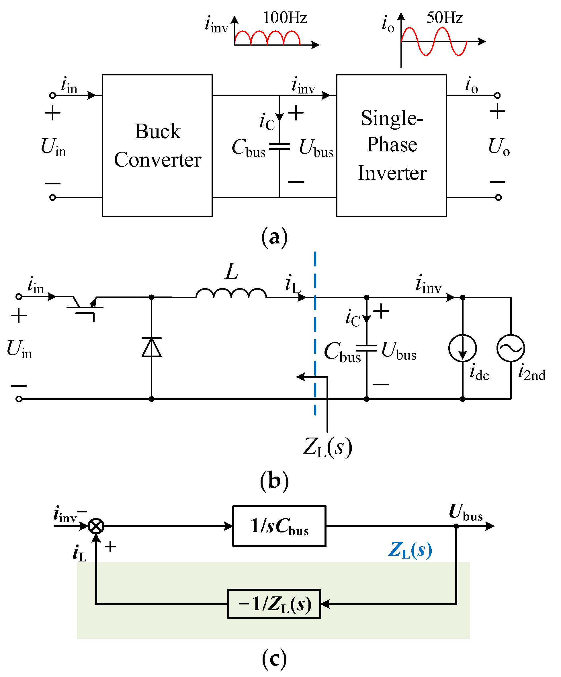
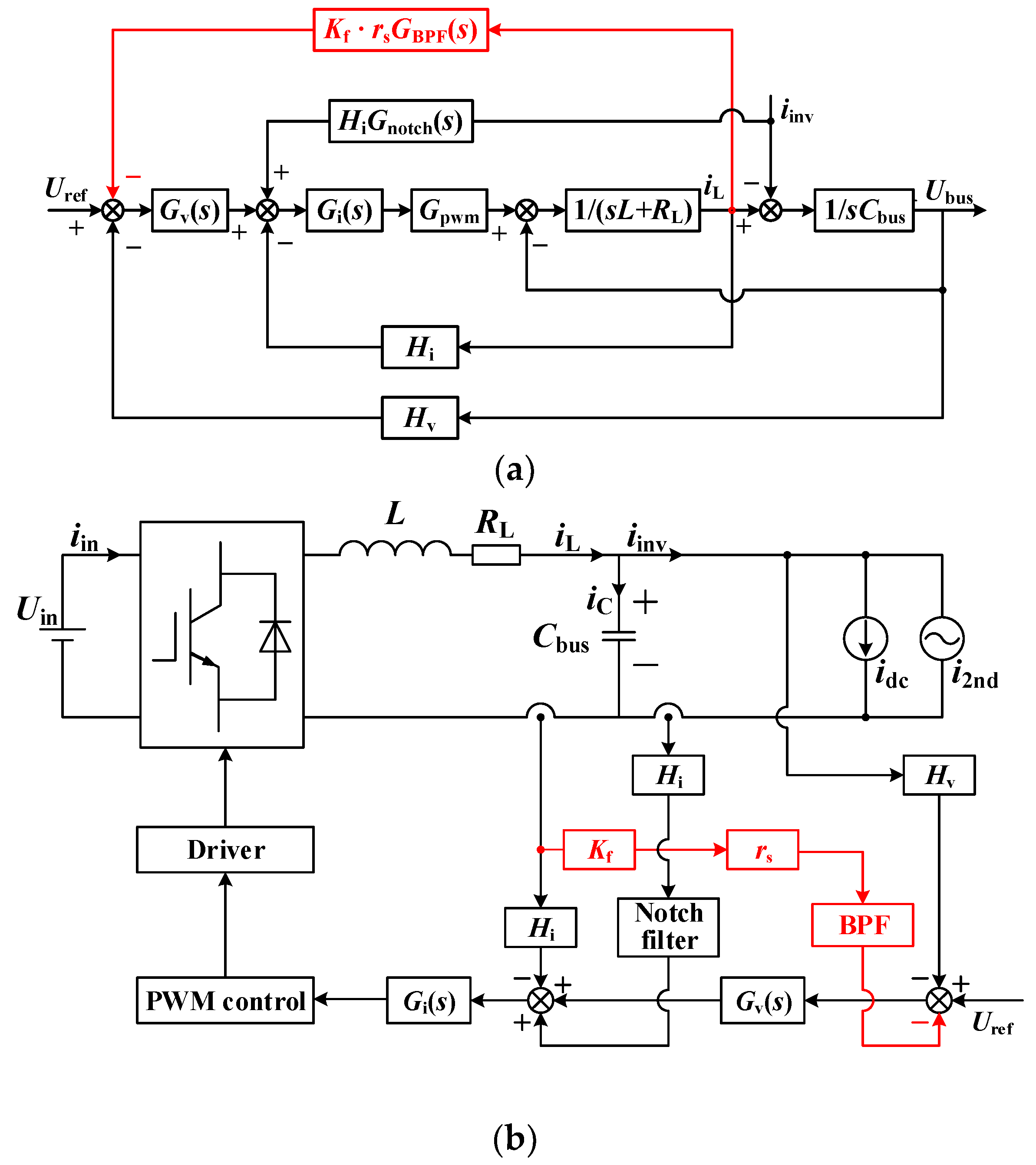
Figure 1a gives the configuration of the two-stage inverter studied in this paper, where the front-end dc-dc converter is a buck converter and the downstream inverter is a single-phase inverter. Figure 1b shows the equivalent schematic diagram. In Figure 1, Uin and iin are the input voltage and input current of the converter, respectively; Cbus and Ubus are the capacitor and voltage of the intermediate dc bus, respectively; io and Uo are the output current and output voltage of the inverter, respectively; iC is the capacitor current; iinv is the input current of the inverter; L is the inductor; iL is the inductor current.

Figure 1.
Two-stage inverter. (a) Configuration; (b) equivalent schematic diagram; (c) block diagram for ZL(s).
The instantaneous output power of the single-phase inverter pulsates at twice the output frequency, and the input current of the inverter can be expressed as [22]
where Um and im are the amplitudes of the output voltage and the output current, respectively; φ is the load impedance angle; ωo is the angular frequency; ωo = 2πfo, and fo is the frequency of the output voltage.
It can be seen from Equation (1) and Figure 1b that iinv is composed of two parts, one is the dc component idc, and the other is the SHC component i2nd, which is provided by the intermediate bus capacitor branch and inductor branch. Hence, the SHC proportion in the front-end buck converter is determined by the inductor branch impedance ZL(s) of the buck converter and the impedance of Cbus at 2fo. Moreover, Cbus is always designed large enough to achieve a very low dc-link voltage ripple, and the SHC in iin is mainly caused by the inductor branch [22,23]. Thus, the SHC suppression in iL can effectively reduce the input power fluctuation and the SHC on the input side.
3. Proposed Control Scheme with New Inductor Current Feedback Path
In this section, a new control method is presented for the SHC reduction and the dynamic performance improvement, which can increase the ZL(s) at 2fo and decrease the ZL(s) at frequencies except for 2fo. Based on Figure 1c, the virtual impedance is introduced into the inductance current branch, then by the transformation and simplification, the novel control method and implementation of the NICFPS are presented.
3.1. Introduction of Virtual Resistor and BPF
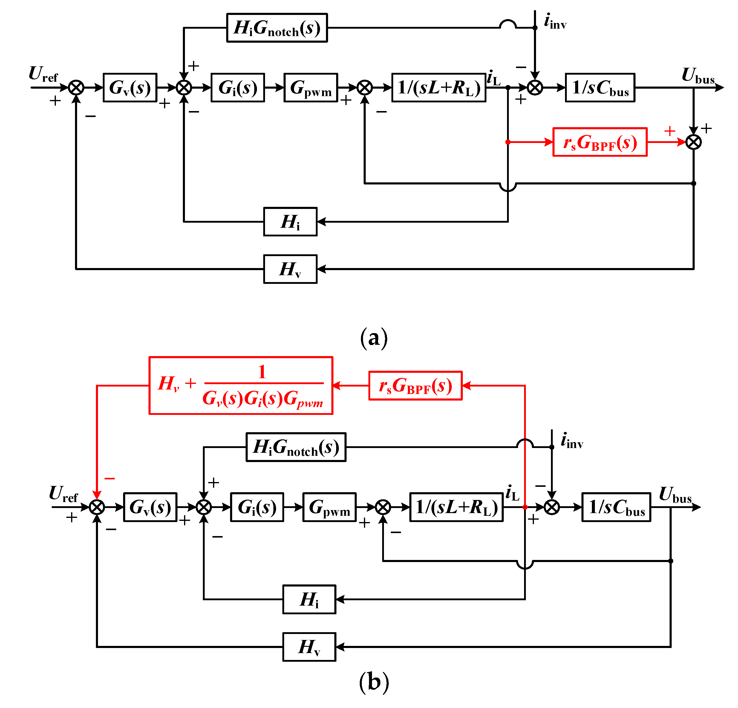
The control block diagram with the introduction of a virtual resistance rs and a BPF is shown in Figure 2a, where Uref is the reference value of bus voltage; Gv(s) is the transfer function of the voltage regulator; Gi(s) is the transfer function of the current regulator; Gnotch(s) is the transfer function of the notch filter; Hv is the voltage feedback gain; Hi is the current feedback gain; RL is the series equivalent resistance of the inductor; Gpwm is the PWM gain; Gpwm = Uin/Vm, and Vm is the amplitude of the carrier.

Figure 2.
Introduction of virtual resistance and BPF. (a) Block diagram; (b) equivalent transformation.
The transfer function of the notch filter can be derived as
where AVF is the gain of the passing frequency range.
The transfer function GBPF(s) of a BPF is expressed as
where ωb is the angular frequency bandwidth.
As seen in Figure 1c and Figure 2a, the introduction of rs and GBPF(s) in Figure 2a can be helpful to increase the ZL(s) of the front-end converter at 2fo, thereby suppressing the SHC. Meanwhile, the crossover frequency of the outer voltage loop in Figure 2a can be increased by changing its parameters. Therefore, the introduction of rs and GBPF(s) in Figure 2a can both suppress the SHC and improve the dynamic performance of the front-end buck converter. Based on Figure 2a, the equivalent transformation is shown in Figure 2b. As seen in Figure 2b, the inductor current feedback function consists of two terms, one is rsGBPF(s), and the other is Hv + 1/(Gv(s)Gi(s)Gpwm). To realize the control scheme, the second term should be simplified.
3.2. Simplification of Feedback Function
To simplify the feedback function in Figure 2b, it is necessary to simplify 1/Gv(s) and 1/Gi(s). The proportion-integral (PI) controller is adopted, then the transfer function GPI(s) and the corner frequency fL can be expressed as
where Kp is the proportional gain; Ki is the integral gain.
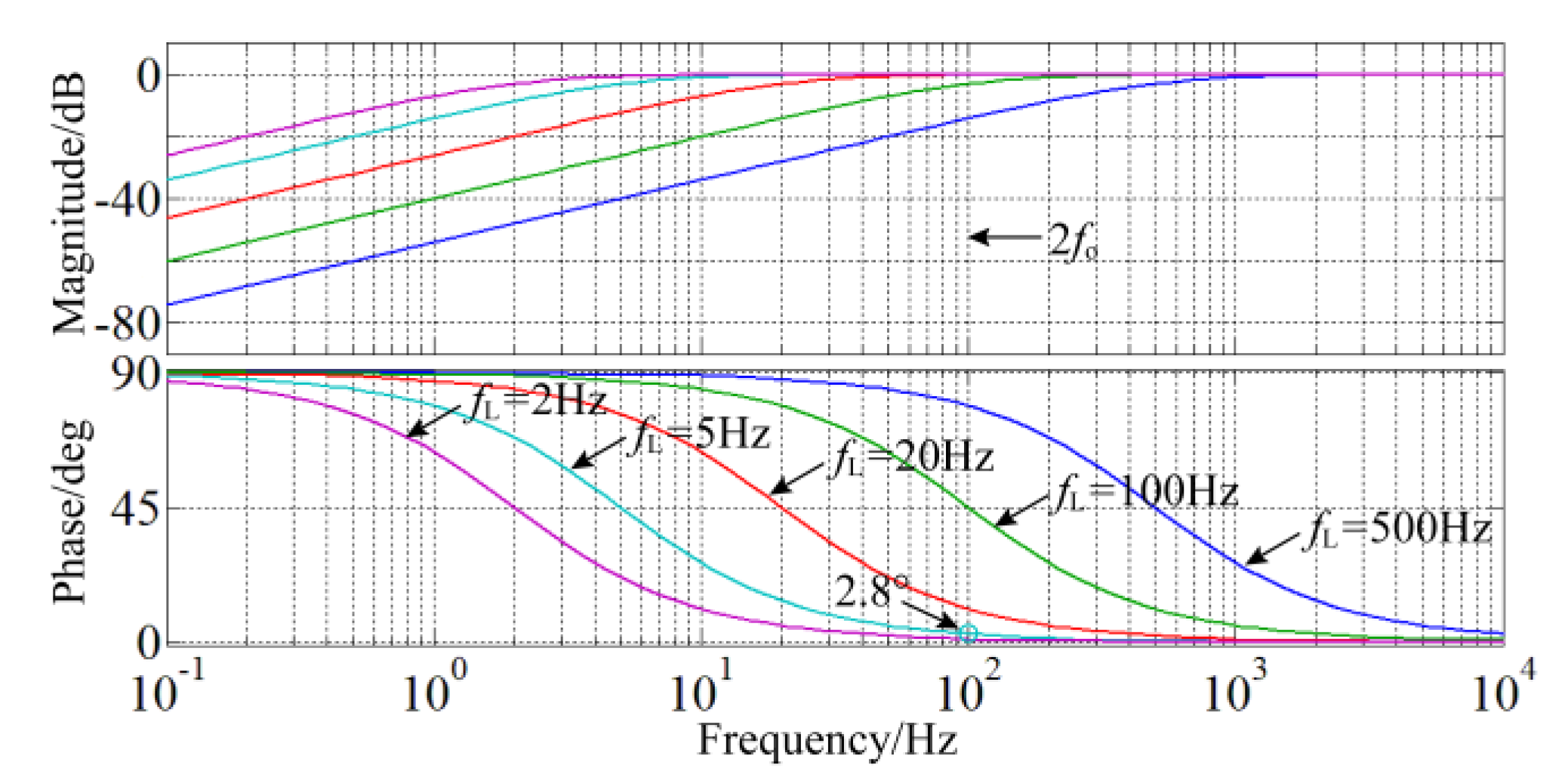
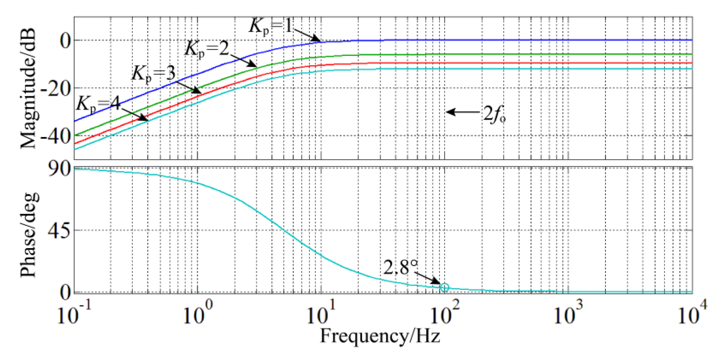
By setting Kp = 1, the Bode diagram of 1/GPI(s) with different fL is shown in Figure 3. As seen with the decrease in fL, the magnitude of 1/GPI(s) is closer to the constant value, and the phase of 1/GPI(s) at 2fo is closer to zero. However, according to Equation (5), the lower integral gain with the lower fL will degrade the steady-state performance of the buck converter. Based on the above analysis, fL = 5 Hz is determined for the PI regulator. When fL = 5 Hz, the phase delay is only 2.8° and the amplitude is almost constant for 1/GPI(s) at 2fo.
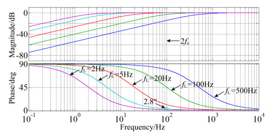
Figure 3.
Bode diagram of 1/GPI(s) with different fL.
When fL = 5 Hz, the Bode diagram of 1/GPI(s) with the different Kp is shown in Figure 4. As seen with the increase in Kp, the amplitude of 1/GPI(s) at 2fo decreases gradually, and the phase of 1/GPI(s) at 2fo almost remains constant. Thus, it is clear that the simplification of 1/GPI(s) is independent of Kp, 1/GPI(s), and Hv + 1/(Gv(s)Gi(s)Gpwm) in the feedback function and can be equivalent to the constant value at 2fo, derived as
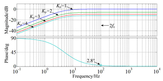
Figure 4.
Bode diagram of 1/GPI(s) with different Kp when fL = 5 Hz.
3.3. Proposed NICFPS and Implementation
After the simplification of the feedback function, the control block diagram of the proposed NICFPS is shown in Figure 5a.
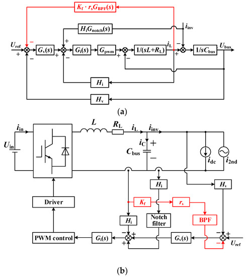
Figure 5.
Proposed NICFPS. (a) Block diagram; (b) implementation.
As seen from Figure 5a, the sampled inductor current, after passing the equivalent gain Kf, the virtual resistance rs and the BPF are fed to the dc bus reference voltage Uref, which is the distinctive feature of the proposed NICFPS. The actual implementation of the NICFPS is shown in Figure 5b and it is obvious that the scheme is easy to implement by software. It should be noted that Figure 5 shows only the equivalent implementation method, the actual meaning of the proposed NICFPS from Figure 2 is to add the virtual resistance between Ubus and iL to reduce the SHC.
4. Parameter Design and Performance Analysis
The main parameters in the feedback function, including the current and voltage regulator parameters, equivalent gain Kf, the virtual resistance rs, and the bandwidth fb of the BPF, will be designed in this section.
The parameters of the inverter prototype are shown in Table 1, which are used for the theoretical analysis, simulation, and experimental verification in this paper.

Table 1.
Parameters of the prototype.
4.1. BPF Parameter Design
The crossover frequency fci of the inner current loop is usually selected to be 1/5 to 1/10 of the switching frequency to guarantee excellent tracking ability [22]. Hence, when 1/10 is selected, we have fci = 1 kHz.
According to Equations (4) and (5), the transfer function of the current regulator at fci can be derived as
where Kpi and fLi are the proportional gain and corner frequency of the current regulator, respectively.
When fLi = 5 Hz, it is evident that fci is much larger than fLi. Hence, according to Equation (9), we have Gi(j2πfci) ≈ Kpi.
The magnitude of the inner current loop has a unity gain at fci. According to Equation (8), (10) can be obtained.
Then from Equation (10), Kpi can be derived as
From Equations (5) and (11), the current regulator is obtained as
For the outer voltage loop, the higher crossover frequency means better dynamic performance. Moreover, the effect of the BPF in the voltage loop is similar to that of the notch filter in the forward path in [22], so the crossover frequency fcv of the voltage loop should be less than the center frequency of the BPF. To improve the dynamic response while reducing the influence of the BPF on the stability margin, fcv = 50 Hz is determined.
Based on Figure 5a, the outer voltage loop gain Tv_NICFPS can be expressed as Equation (13). The magnitude of the outer voltage loop has a gain unity at fcv, then Equation (14) is obtained.
According to Equation (14), the proportional gain Kpv of the voltage regulator can be derived as
From Equations (5) and (15), the voltage regulator is derived as
Based on Equations (7), (12) and (16), the equivalent gain Kf in the feedback function can be obtained.
4.2. Determination of Virtual Resistor Value
The SHC suppression ratio is used to determine the minimum value of the virtual resistor. By setting the reference voltage to zero, the control block diagram in Figure 5a can be equivalently transformed into that in Figure 6.
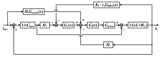
Figure 6.
Block diagram for the gain from iinv to iL.
Based on Figure 6, the transfer function Gii(s) from iinv to iL can be derived as Equation (17). The corner frequency fLv of the voltage regulator is much lower than 2fo, hence when fLv = 5 Hz, we have Gv(j2π·2fo) ≈ Kpv. For the reason that 2fo is the center frequency of both the BPF and the notch filter, the magnitude of GBPF(s) is around 1 at 2fo, and the magnitude of Gnotch(s) is nearly 0 at 2fo.
Defining |Gii(j2π·2fo)| as the SHC suppression ratio and α as the SHC suppression requirement, then Equation (18) can be obtained from Equation (17). In general, α is required to be less than 5%, i.e., α ≤ 5% [19]. When α is set to 5%, by substituting Equations (11) and (15) into (18), it can be deduced that the requirement of virtual resistance is rs ≥ 15.5 Ω.
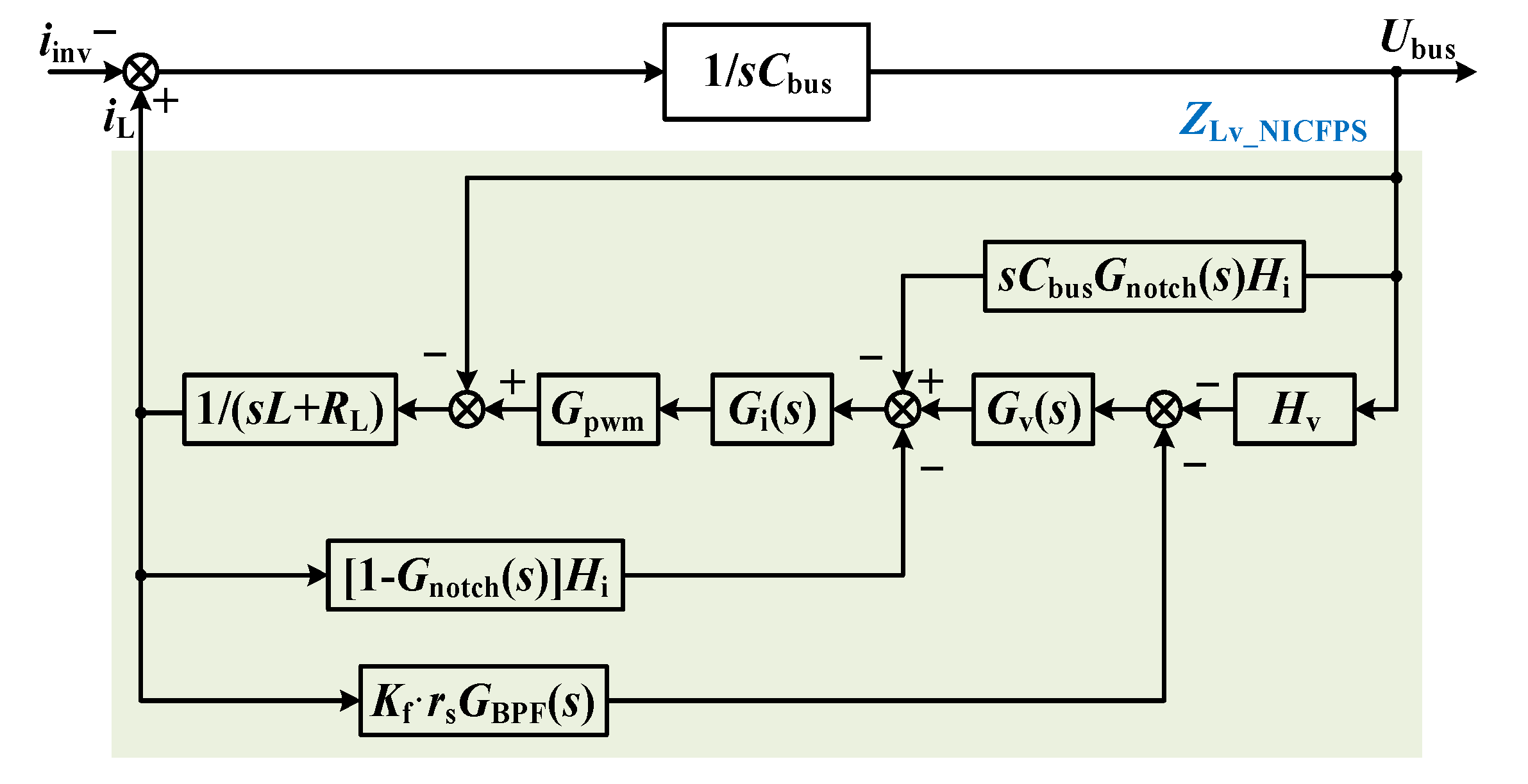
To obtain the inductor branch impedance ZLv_NICFPS(s), Uref in Figure 5a is set to 0, then the block diagram in Figure 5a can be transformed into that shown in Figure 7. Based on Figure 7, the inductor branch impedance can be obtained as Equations (19) and (20). When α ≤ 5% and rs ≥ 15.5 Ω, the magnitude plots of ZLv_NICFPS(s) with different rs are shown in Figure 8.

Figure 7.
Block diagram for ZLv_NICFPS(s) of the proposed scheme.
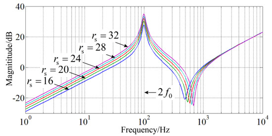
Figure 8.
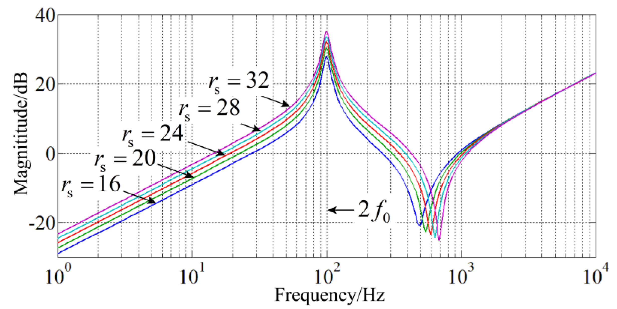
Magnitude plots of ZLv_NICFPS(s) with different rs.
As can be seen from Figure 8, ZLv_NICFPS(s) will increase with the increase in rs in the wide frequency range near 2fo, which shows that the SHC suppression capability will improve, but the dynamic performance will deteriorate. The reason is that the actual BPF is not ideal, rs will affect the inductor branch impedance not only at 2fo but also at frequencies except for 2fo. In view of both the SHC and the dynamic performance, rs = 20 Ω is determined.
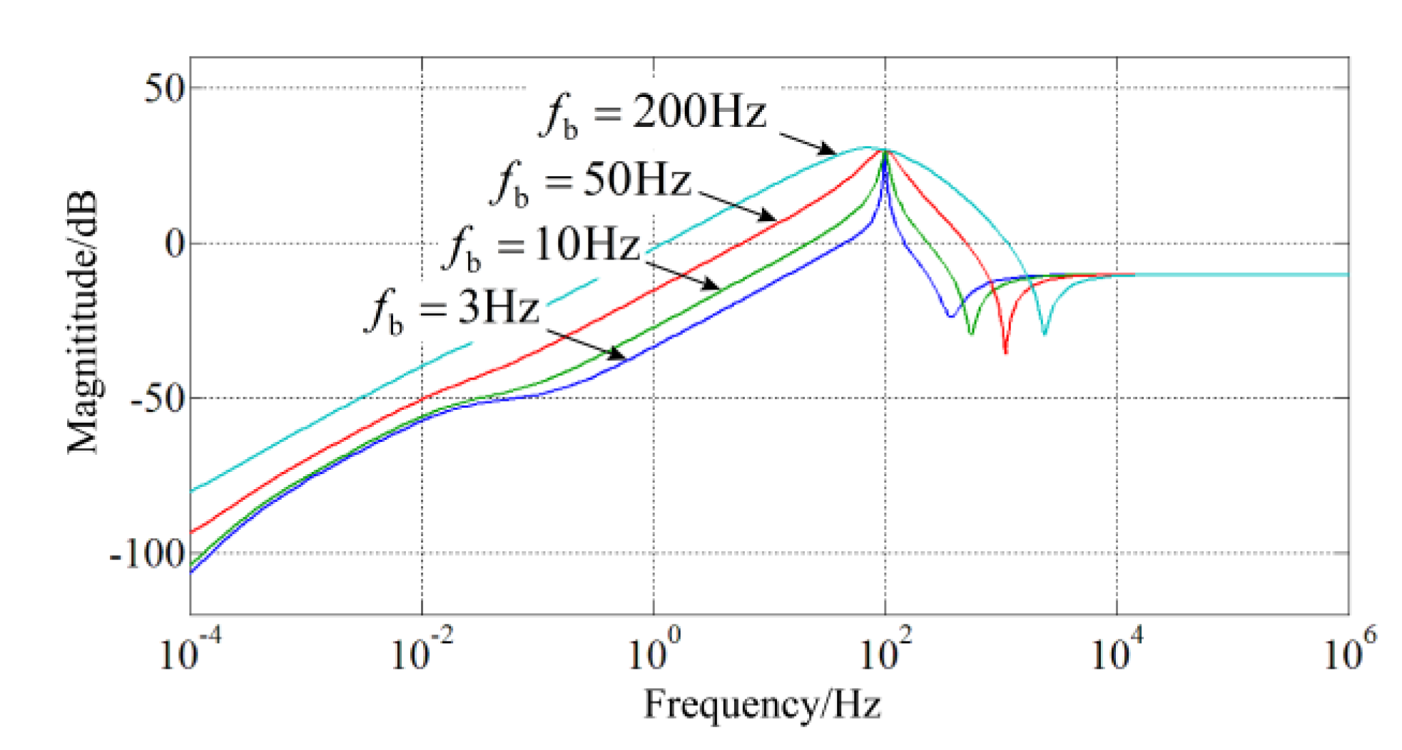
4.3. Design of Bandwidth for BPF
Figure 9 shows the magnitude plots of the ZLv_NICFPS(s) with different BPF bandwidth fb. It is obvious that, as fb increases, ZLv_NICFPS(s) grows larger at low frequency, decreasing the dynamic response. Thus, fb should not be too large in view of the dynamic performance. Meanwhile, when fb is too small, such as the value lower than 10 Hz, the magnitude change of ZLv_NICFPS(s) at low frequency is not quite obvious. Moreover, fb should be greater than the fluctuation range of 2fo [15,18]. Thus, in /the inverter illustrated in Table 1, fb in the feedback function is designed as 10 Hz.
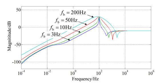
Figure 9.
Magnitude plots of ZLv_NICFPS(s) with different fb.
4.4. Output Impedance Comparison
The magnitude of the output impedance can be used to evaluate the performance of SHC reduction and dynamic response during the load transient. The higher magnitude of the output impedance at 2fo means the better ability for SHC reduction, and the lower magnitude at frequencies except for 2fo means the lower bus voltage overshoot and undershoot during the load transient.
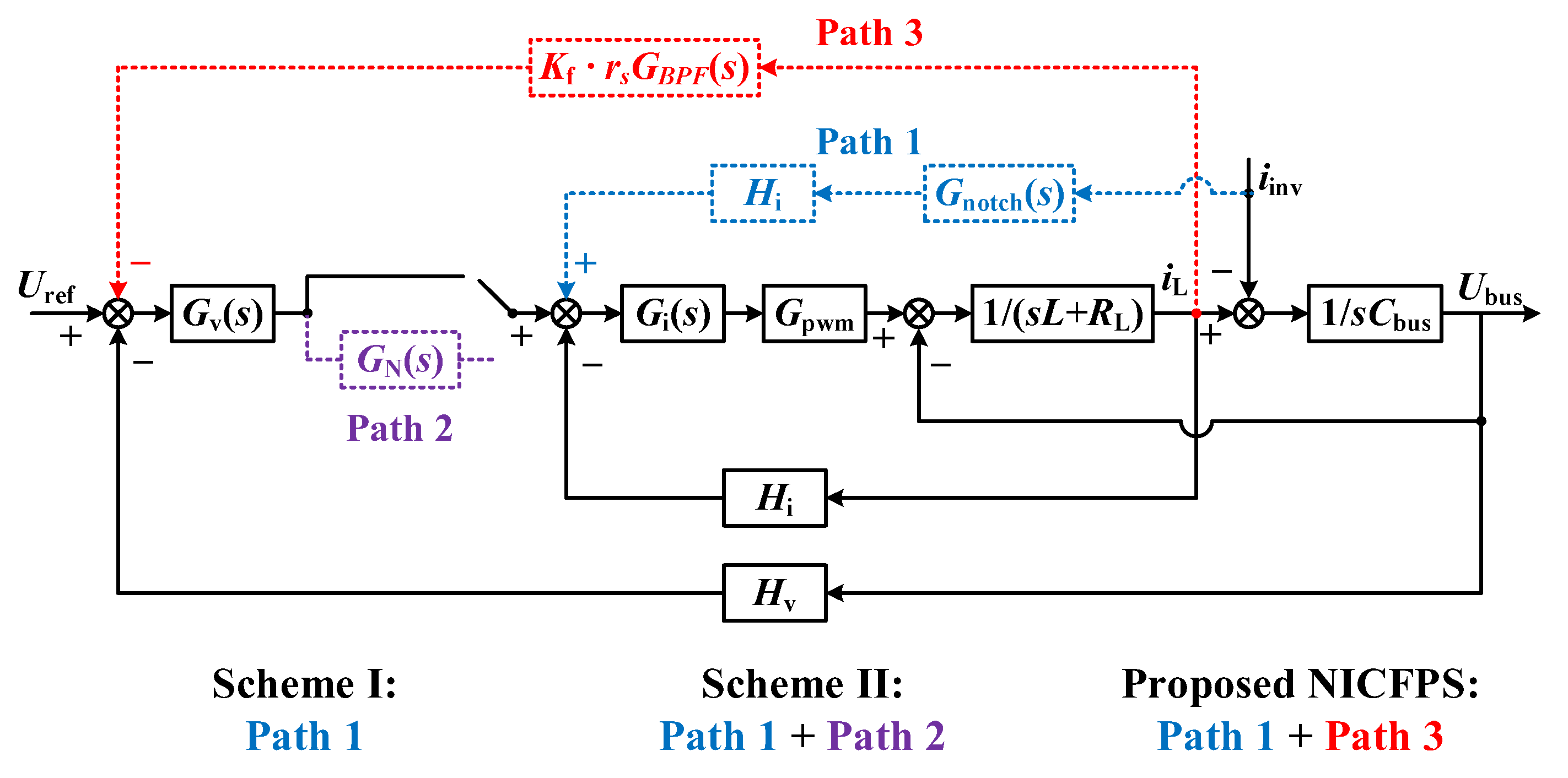
In the existing typical control schemes, the NF-LCFFS and NF-CR+LCFFS in [22] have a relatively high performance of SHC reduction and dynamic response. Hence, to evaluate the performance of the proposed NICFPS, this section compares the output impedance among the proposed NICFPS and the two abovementioned schemes, in which scheme I and scheme II indicate the NF-LCFFS and NF-CR+LCFFS, respectively.
The block diagram of the three schemes is shown in Figure 10. Compared with scheme II, the proposed NICFPS requires the additional parameter design for rs, fb, and Kf, however, the parameters can be easily determined only by the simple calculation and output impedance comparison as described in Section 4.

Figure 10.
Control block diagram of the three schemes: Scheme I and Scheme II are both from Reference [22].
In the three schemes, the parameters of the current regulator and crossover frequency of the inner current loop are the same. In order to reduce the SHC effectively, the crossover frequency of the outer voltage loop is selected as 10 Hz in scheme I, and 50 Hz in both scheme II and the proposed NICFPS.
Based on Figure 10 in this paper and Equations (21) and (23) in the Reference [22], inductor branch impedance at 2fo for schemes I and II can be derived as
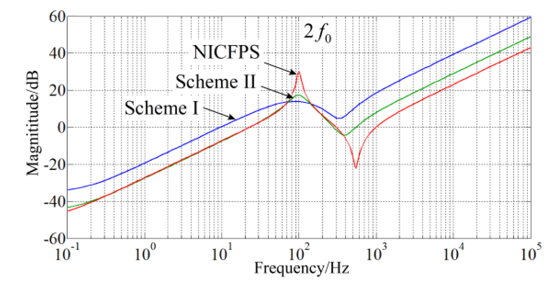
According to Equations (20)–(22), the magnitude plots of the inductor branch impedance of the buck converter with the three schemes are shown in Figure 11. It can be seen from Figure 11 that, at frequencies except for 2fo, the proposed NICFPS and scheme II have lower output impedance, which means better dynamic performance. Moreover, the proposed NICFPS has the highest output impedance at 2fo, which indicates the best SHC suppression ability among the three schemes.
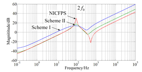
Figure 11.
Magnitude plots of output impedance.
5. Simulation Results
To verify the effectiveness of the proposed NICFPS, the simulation results of about a 10 kW two-stage inverter with the parameters in Table 1 are provided. The simulation model is built by MATLAB software, and based on that, the proposed NICFPS and the two typical schemes are tested.
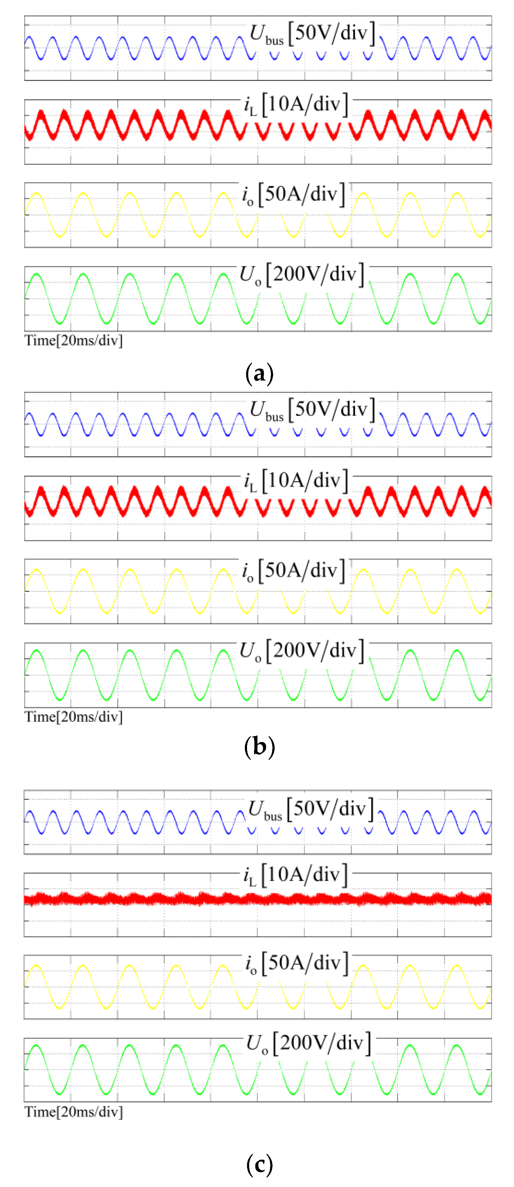
Figure 12 shows the steady-state simulation results of the three schemes with the 10 kW output power. As seen, the SHC proportion in iL is around 4.3% in the NICFPS, while 32.6% in scheme I and 10% in scheme II. It is obvious that the proposed NICFPS has the best ability to suppress the SHC, and the reason is that the scheme has the highest output impedance at 2fo, which can be seen in Figure 11.
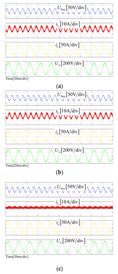
Figure 12.
Steady-state simulation results. (a) Scheme I; (b) Scheme II; (c) proposed NICFPS.
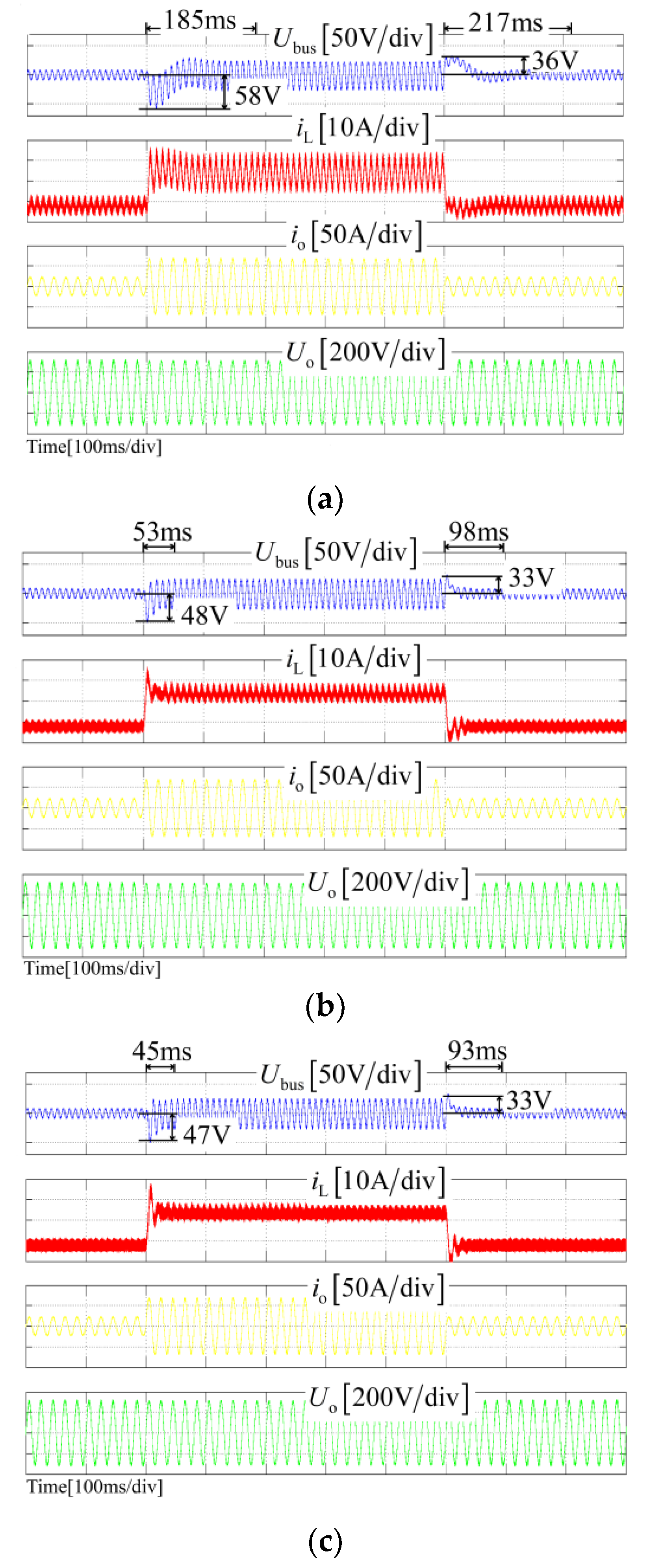
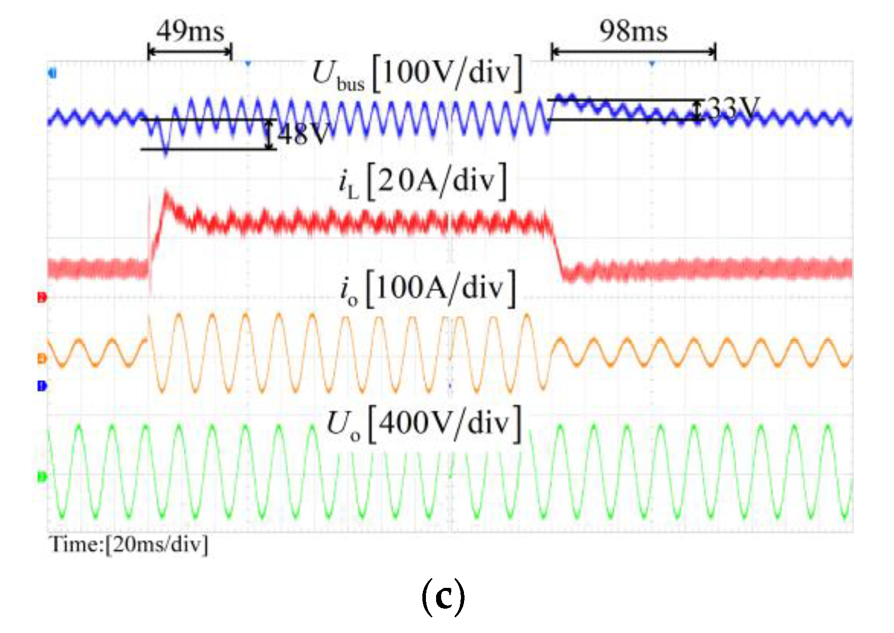
Figure 13 shows the dynamic simulation results of the three schemes, and the load of the inverter changes between 33% and 100% full load. As seen, in the proposed NICFPS and scheme II, the undershoots of Ubus are both close to 50 V and the settling times are both about 50 ms when the load steps up, the overshoots of Ubus are both 33 V, and the settling times are both nearly 100 ms when the load steps down. However, in the scheme I, the settling time is about 200 ms, and the undershoot and overshoot are 58 V and 36 V, respectively. It can be seen from Figure 13 that scheme I has the evident overshoot and undershoot during the load transient, and the proposed NICFPS and scheme II have better dynamic performance. This is because scheme I has the highest output impedance almost at all frequencies, but the proposed NICFPS and scheme II can reduce the output impedance at the frequencies except for 2fo, and the characteristic comparison of the output impedance among the three schemes can be seen from Figure 11.
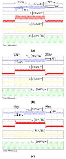
Figure 13.
Dynamic simulation results between 33% and 100% full load. (a) Scheme I; (b) Scheme II; (c) proposed NICFPS.
Based on Figure 12 and Figure 13, Table 2 gives the simulation results of the three control schemes in terms of the SHC proportion and voltage fluctuation during load transient. The results in Table 2 show that the proposed NICFPS has both the best ability to suppress SHC and good dynamic performance. Moreover, the simulation results are in accordance with the theoretical analysis in Section 4.
Table 2.
Simulation results comparison.
6. Experimental Results
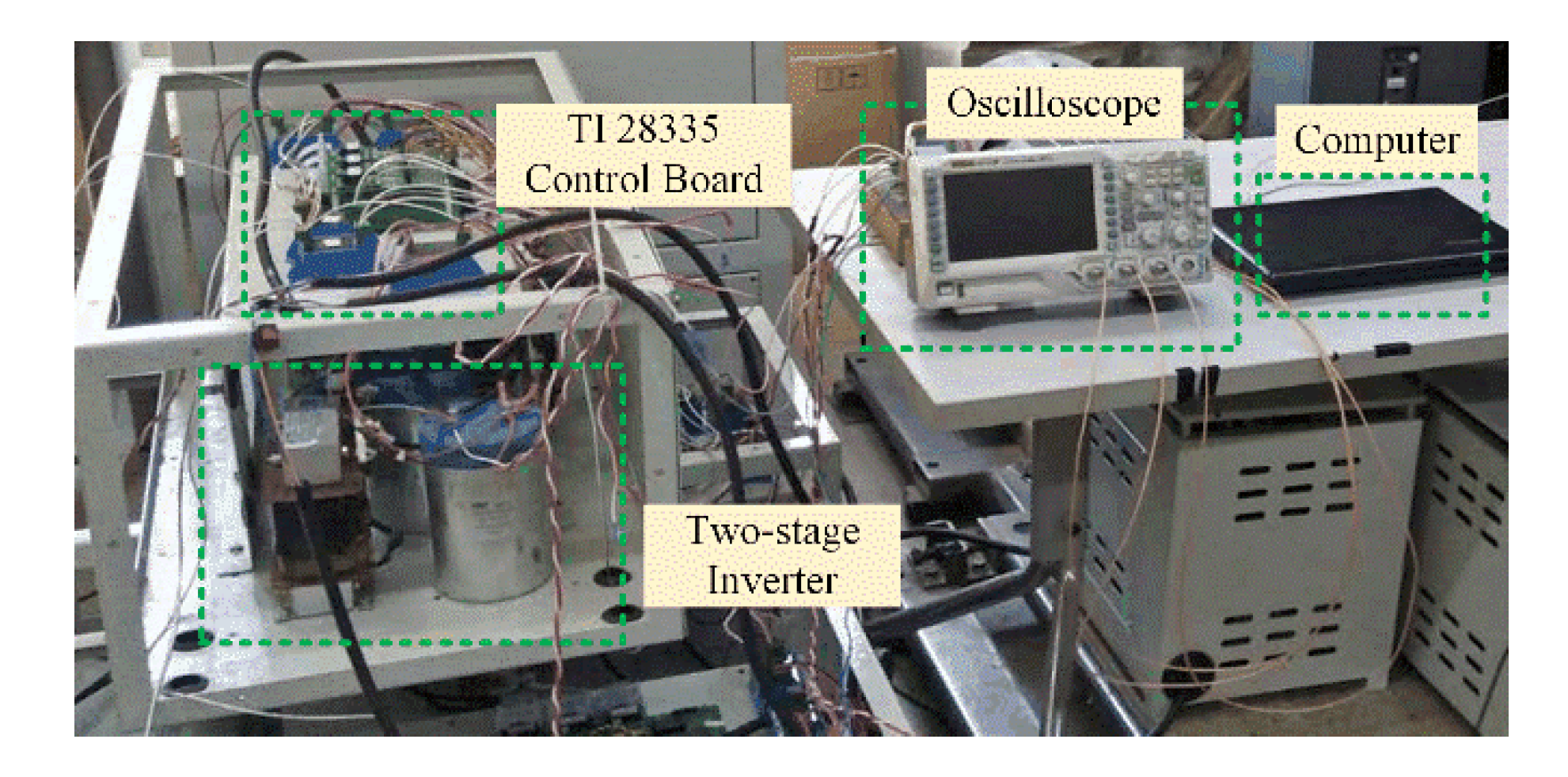
To further verify the aforementioned theoretical analysis and simulation results, a 10 kW prototype is developed and tested with the three control schemes, namely, scheme I (NF-LCFFS), scheme II (NF-CR+LCFFS), and the proposed NICFPS. The experimental platform is shown in Figure 14, which mainly consists of a two-stage inverter, a control board, an oscilloscope, and a debugging computer. The two-stage inverter is composed of a front-end buck converter and a downstream single-phase inverter. The microprocessor of the inverter is TMS320F28335 from TI company. The parameters of the prototype are listed in Table 1.
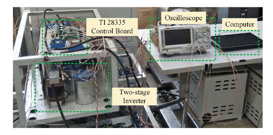
Figure 14.
Experimental platform.
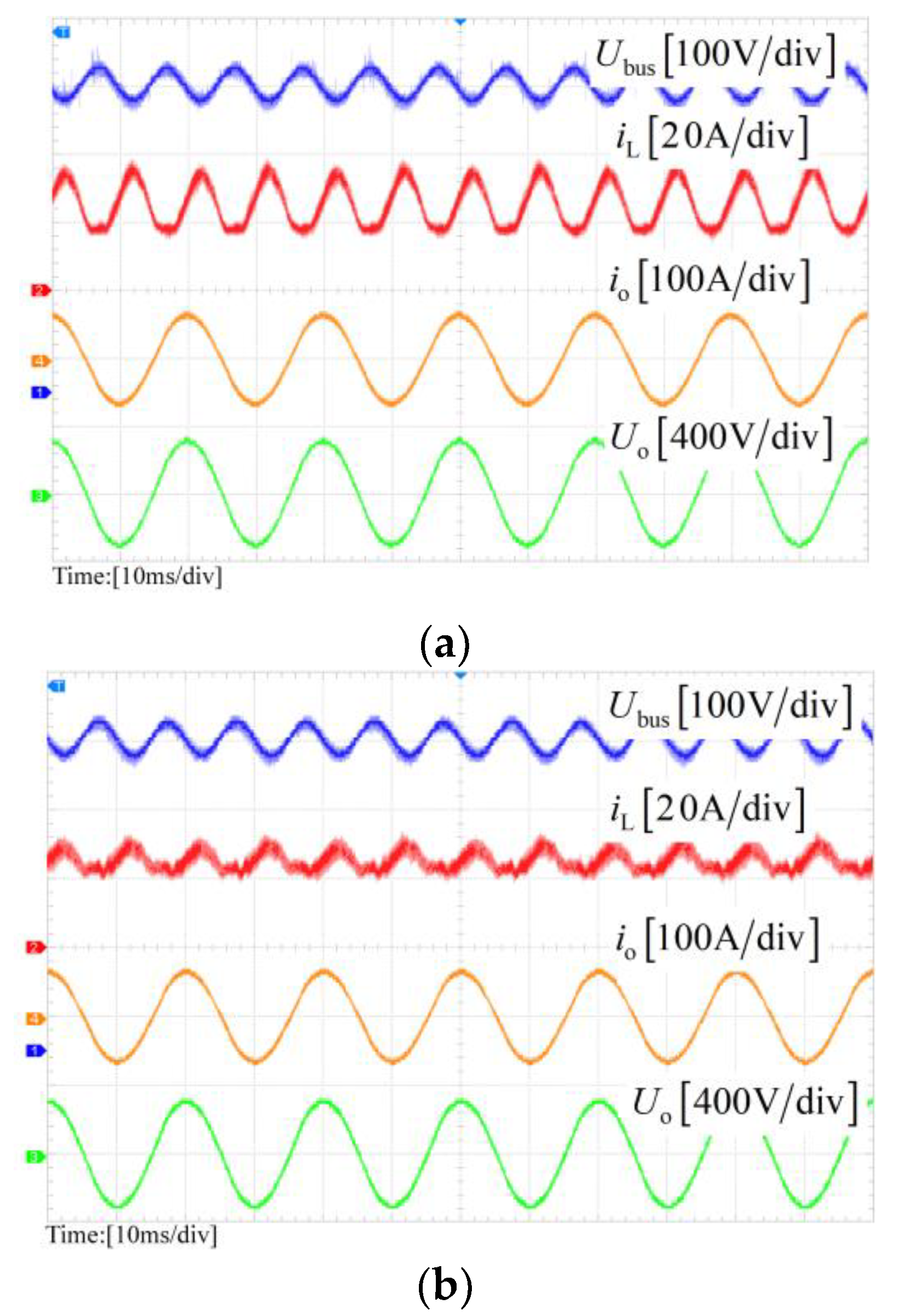
Figure 15 shows the steady-state experimental results of the three schemes with 10 kW ac output power. It can be seen from Figure 15 that the SHC proportion in the proposed NICFPS is about 4.7%, while in scheme I it is 33.2% and in scheme II it is 11.1%. Thus, it is clear that the proposed NICFPS has the best effect on the SHC reduction because the highest output impedance at 2fo can be obtained for the scheme as shown in Figure 11.
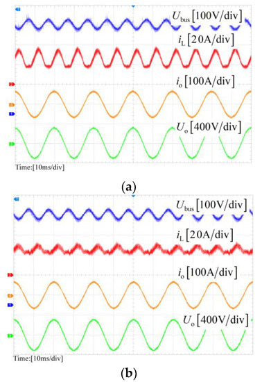
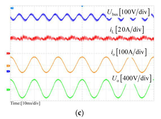
Figure 15.
Steady-state experimental results. (a) Scheme I; (b) Scheme II; (c) proposed NICFPS.
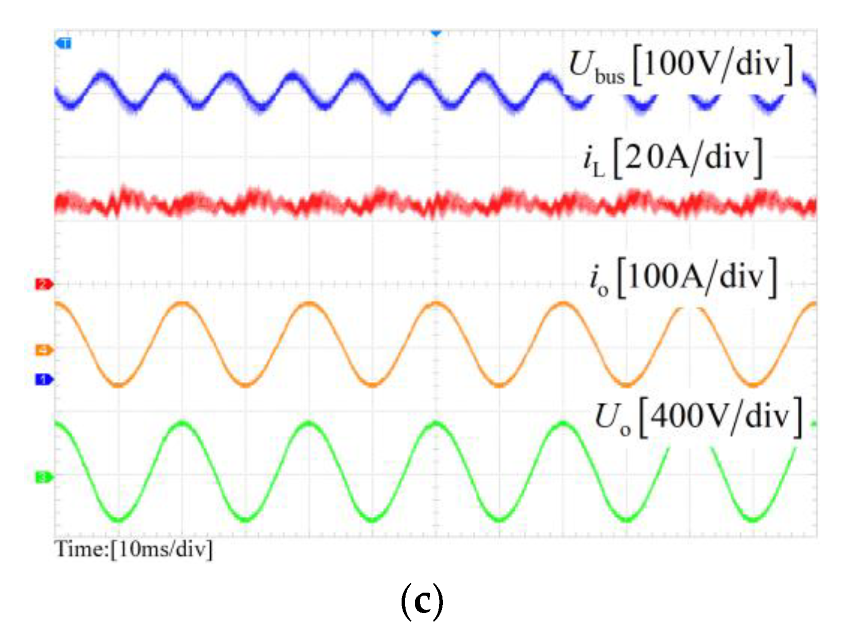
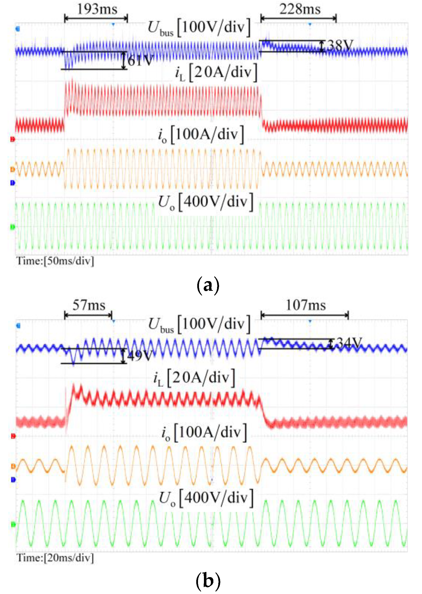
Figure 16 shows the dynamic experimental results of the three schemes, and the ac load of the inverter changes between 33% and 100% full load. In the proposed NICFPS and scheme II, the undershoots of Ubus are both close to 50 V and the settling times are both about 50 ms when the load steps up, the overshoots of Ubus are both 33 V, and the settling times are both nearly 100 ms when the load steps down. However, in scheme I, the settling time is even close to 230 ms, and the undershoot and overshoot are 61 V and 38 V, respectively. It is obvious that the NICFPS and scheme II have better dynamic performance. The reason is that the proposed NICFPS and scheme II can reduce the output impedance at the frequencies except for 2fo, which can be seen in Figure 11.
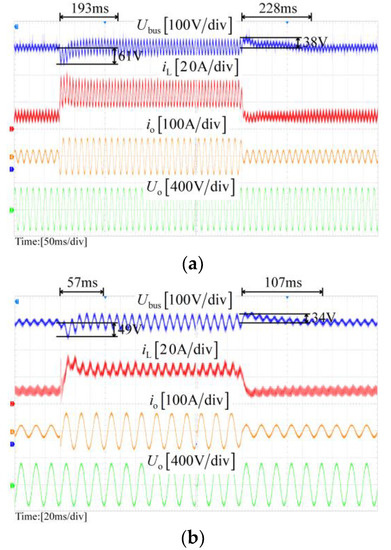

Figure 16.
Dynamic experimental results between 33% and 100% full load. (a) Scheme I; (b) Scheme II; (c) proposed NICFPS.
Table 3 summarizes the experimental results comparison of the three control schemes in terms of the SHC proportion and the bus voltage fluctuation when the output power step changes between a 33% and 100% rated load. As seen, the proposed NICFPS has the best ability to suppress the SHC since it has the highest magnitude of the output impedance at 2fo. Meanwhile, due to the lower output impedance at the frequencies except for 2fo, the proposed NICFPS and scheme II have better dynamic performance than scheme I.
Table 3.
Experimental results comparison.
In brief, among the three control schemes, the proposed NICFPS has the best SHC reduction ability and dynamic performance. Furthermore, comparing the SHC proportion, overshoot, and undershoot in Table 3 with those in Table 2, it can be seen that the experimental results are well in agreement with the simulation results in Section 5 and the theoretical analysis in Section 4.
7. Conclusions
This paper focuses on the SHC reduction for the two-stage inverter with the front-end buck converter. To reduce the SHC, the virtual resistance and the BPF in a new feedback path are introduced to increase the output impedance at 2fo, and the control method of the NICFPS is proposed after simplifying the feedback function. In consideration of both the SHC reduction and the dynamic response improvement, the parameter design approach for the feedback function is further presented for the proposed NICFPS. The implementation method of the NICFPS is illustrated, and the output impedance derivation and the performance analysis are provided, which indicate that compared to the existing control methods, the proposed NICFPS can remarkably decrease the SHC while still maintaining good dynamic performance. The simulation model and the experimental prototype for a 10 kW two-stage inverter are built and tested, and simulation and experimental results verify the effectiveness of the proposed control scheme. The SHC proportion can be reduced to about 4.7% in the proposed NICFPS, 33.2% in scheme I, and 11.1% in scheme II. The undershoot and settling time can be reduced close to 50 V and 50 ms in the proposed NICFPS, and 61 V and 230 ms in scheme I.
Author Contributions
Conceptualization, J.X. and H.D.; methodology, simulation, and experiment, H.D.; resources, J.X.; writing—original draft preparation, H.D.; writing—review and editing, J.X.; supervision, J.X. All authors have read and agreed to the published version of the manuscript.
Funding
This research received no external funding.
Institutional Review Board Statement
Not applicable.
Informed Consent Statement
Not applicable.
Data Availability Statement
Not applicable.
Conflicts of Interest
The authors declare no conflict of interest.
References
- Kan, S.; Ruan, X.; Huang, X.; Dang, H. Second harmonic current reduction for flying capacitor clamped boost three-level converter in photovoltaic grid-connected inverter. IEEE Trans. Power Electron. 2021, 36, 1669–1679. [Google Scholar] [CrossRef]
- Zhou, H.; He, L.; Lin, Z. Low frequency current ripple suppression for two-stage single-phase inverter based on impedance editing. IEEE Trans. Ind. Electron. 2022, 69, 13417–13427. [Google Scholar] [CrossRef]
- Liu, F.; Ruan, X.; Huang, X.; Qiu, Y.; Jiang, Y. Control scheme for reducing second harmonic current in AC-DC-AC converter system. IEEE Trans. Power Electron. 2022, 37, 2593–2604. [Google Scholar] [CrossRef]
- Kan, S.; Ruan, X.; Dang, H.; Zhang, L.; Huang, X. Huang. Second harmonic current reduction in front-end DC−DC converter for two-stage single-phase photovoltaic grid-connected inverter. IEEE Trans. Power Electron. 2019, 34, 6399–6410. [Google Scholar] [CrossRef]
- Zhang, L.; Ruan, X. Control schemes for reducing second harmonic current in two-stage single-phase converter: An overview from DC-bus port-impedance characteristics. IEEE Trans. Power Electron. 2019, 34, 10341–10358. [Google Scholar] [CrossRef]
- McGrath, B.P.; Holmes, D. A general analytical method for calculating inverter DC-link current harmonics. IEEE Trans. Ind. Appl. 2009, 45, 1851–1859. [Google Scholar] [CrossRef]
- Kwon, J.; Kim, E.; Nam, K. High-efficiency fuel cell power conditioning system with input current ripple reduction. IEEE Trans. Ind. Electron. 2009, 56, 826–834. [Google Scholar]
- Sullivan, C.; Awerbuch, J.; Latham, A. Decrease in photovoltaic power output from ripple: Simple general calculation and the effect of partial shading. IEEE Trans. Power Electron. 2013, 28, 740–747. [Google Scholar] [CrossRef]
- Giustiniani, A.; Petrone, G.; Spagnuolo, G.; Vitelli, M. Low-frequency current oscillations and maximum power point tracking in grid-connected fuel-cell-based systems. IEEE Trans. Ind. Electron. 2010, 57, 2042–2053. [Google Scholar] [CrossRef]
- Itoh, J.; Hayashi, F. Ripple current reduction of a fuel cell for a single-phase isolated converter using a DC active filter with a center tap. IEEE Trans. Power Electron. 2010, 25, 550–556. [Google Scholar] [CrossRef]
- Cai, W.; Liu, B.; Duan, S.; Jiang, L. An active low-frequency ripple control method based on the virtual capacitor concept for BIPV systems. IEEE Trans. Power Electron. 2014, 29, 1733–1745. [Google Scholar] [CrossRef]
- Zhang, L.; Ruan, X.; Ren, X. One-cycle control for electrolytic capacitor-less second harmonic current compensator. IEEE Trans. Power Electron. 2018, 33, 1724–1739. [Google Scholar] [CrossRef]
- Huang, X.; Ruan, X.; Fang, J. A virtual impedance based control scheme for modular electrolytic capacitor-less second harmonic current compensator. IEEE Trans. Ind. Electron. 2021, 68, 198–209. [Google Scholar] [CrossRef]
- Liu, F.; Ruan, X.; Huang, X. Second harmonic current reduction for two-stage inverter with DCX-LLC resonant converter in front-end DC–DC converter: Modeling and control. IEEE Trans. Power Electron. 2021, 36, 4597–4609. [Google Scholar] [CrossRef]
- Shi, Y.; Liu, B.; Duan, S. Low-frequency input current ripple reduction based on load current feedforward in a two-stage single-phase inverter. IEEE Trans. Power Electron. 2016, 31, 7972–7985. [Google Scholar] [CrossRef]
- Wang, W.; Ruan, X. A modified reference of an intermediate bus capacitor voltage-based second-harmonic current reduction method for a standalone photovoltaic power system. IEEE Trans. Power Electron. 2016, 31, 5562–5573. [Google Scholar] [CrossRef]
- Gambhir, A.; Mishra, S.; Joshi, A. Power frequency harmonic reduction and its redistribution for improved filter design in current-fed switched inverter. IEEE Trans. Ind. Electron. 2019, 66, 4319–4333. [Google Scholar] [CrossRef]
- Wang, D.; Nahid-Mobarakeh, B.; Emadi, A. Second harmonic current reduction for a battery-driven grid interface with three-phase dual active bridge DC/DC converter. IEEE Trans. Ind. Electron. 2019, 66, 9056–9064. [Google Scholar] [CrossRef]
- Zhang, L.; Ren, X.; Ruan, X. A bandpass filter incorporated into the inductor current feedback path for improving dynamic performance of the front-end DC-DC converter in two-stage inverter. IEEE Trans. Ind. Electron. 2014, 61, 2316–2325. [Google Scholar] [CrossRef]
- Liu, C.; Lai, J. Low frequency current ripple reduction technique with active control in a fuel cell power system with inverter load. IEEE Trans. Power Electron. 2007, 22, 1429–1436. [Google Scholar] [CrossRef]
- Wei, Z.; Deng, X.; Gong, C.; Chen, J.; Zhang, F. A novel technique of low frequency input current ripple reduction in two-stage DC-AC inverter. In Proceedings of the IEEE Indsutrial Electronics Conference, Montreal, QC, Canada, 25–28 October 2012. [Google Scholar]
- Zhu, G.; Ruan, X.; Zhang, L.; Wang, X. On the reduction of second harmonic current and improvement of dynamic response for two-stage single-phase inverter. IEEE Trans. Power Electron. 2015, 30, 1028–1041. [Google Scholar] [CrossRef]
- Zhang, L.; Ruan, X.; Ren, X. Second-harmonic current reduction and dynamic performance improvement in the two-stage inverters: An output impedance perspective. IEEE Trans. Ind. Electron. 2015, 62, 394–404. [Google Scholar] [CrossRef]

Publisher’s Note: MDPI stays neutral with regard to jurisdictional claims in published maps and institutional affiliations. |
© 2022 by the authors. Licensee MDPI, Basel, Switzerland. This article is an open access article distributed under the terms and conditions of the Creative Commons Attribution (CC BY) license (https://creativecommons.org/licenses/by/4.0/).