1. Introduction
Semiconductor power modules (IGBT, MOSFET, IGCT, etc.) are the key components of power electronic systems. They are widely used in industrial systems such as high-speed rail and electromagnetic equipment, makingsemiconductor devices often in a complex working environment. In this way, the safety and stability of power electronic equipment may be affected, resulting in incalculable economic losses [
1]. In the investigation of various failure factors, the proportion of high temperature-induced failures is as high as 55% [
2]. The accurate prediction of the maximum temperature in the chip is essential for evaluating the reliability and lifetime of power semiconductor modules, ensuring the safe operation of power electronics, and conducting heat dissipation design [
3,
4].
IGBT chips generate power losses during operation, and the losses in the form of joule heat make the chip virtual junction temperature (
Tvj) increase, which affects the electrical characteristics of the IGBT module. Circuit systems at steady second-scale generally use the virtual junction temperature (
Tvj) of the chip to characterize the thermal impedance parameters of the IGBT module as well as to achieve reliability predictions [
5]. It is worth noting that the virtual junction temperature (
Tvj) is an equivalent description of the chip junction region. The high voltage and high current shocks occurring during the switching transient process will aggravate the temperature distribution along the chip vertical path, making the maximum temperature of the chip much higher than the junction temperature. At this time, if the virtual junction temperature (
Tvj) is used to evaluate the reliability of the IGBT module, it may cause the uncontrollable failure of the module. The cell-level finite element model can evaluate the temperature distribution along the chip vertical path [
6], but for complex circuit models with multiple timescales’ joint simulations, it is inefficient or even difficult to assess the temperature distribution. Therefore, researchers are in urgent need of a thermal network model that can accurately reflect the short-time transient maximum temperature of IGBT chips in a steady second-scale circuit system, which is of great theoretical significance and application value for assessing the reliability of the devices and guiding the design of power electronics.
Currently, scholars have carried out a lot of research on acquiring the temperature distribution of IGBT chips. Finite element models of the IGBT module are mainly established to acquire the maximum temperature of the chip surface [
7,
8]. References [
9,
10] partitioned the chip surface according to its inhomogeneous current density; they proposed a field-way bidirectional coupling multi-rate simulation method based on Comsol-Simulink to accurately obtain the temperature distribution and maximum temperature of the chip surface. However, according to the physical principles of semiconductor devices, it is known that the peak electric field inside the chip is located at the junction of the reverse bias PN junction [
11], rather than the chip surface. Therefore, in reference [
12], an analytical model of the temperature distribution along the vertical path was established according to the thermal diffusion equation, and the temperature distribution of the chip under short-circuit conditions was predicted, indicating that the maximum temperature inside the chip was located at the reverse bias junction. In [
13], by building a two-dimensional TCAD finite element model of a field-stop IGBT chip, the effect of the peak electric field on the temperature distribution inside the chip was shown. In [
5,
14], the heat source in the active area of the finite element model was divided into surface heat source and body heat source according to the on-state voltage drop distribution of the IGBT chip, and it concluded that the loading of the distributed heat source can predict the chip junction temperature more accurately; Reference [
15] performed the IGBT module longitudinal cut to obtain the cross temperature distribution of the seven-layer structure of the module, but there were only two monitoring points along the chip vertical path, and the temperature distribution during the switching transient could not be obtained due to the limitation of the sampling frequency of the thermal imager.
To sum up, the steady second-scale systems are necessarily mixed with transient processes with small electromagnetic time constants, which determine whether the device can operate reliably [
16]. Therefore, the prediction of the short-duration transient temperature characteristics along the chip vertical path must be achieved in long time scales. Since the losses along the chip vertical path of the IGBT chip have both distributed and time-varying characteristics during the switching transient, the lack of a reasonable simplified modeling method makes it difficult to achieve an accurate evaluation of the temperature distribution and efficient joint multi-timescale simulation.
To address the shortcomings of the existing research status, this paper fully considers the effects of distributed heat sources and chip sublayer division methods on temperature distribution along the chip vertical path in the short-duration transient microsecond-scale. First, the distributed heat source model along the chip vertical path is established based on the physical principle of semiconductor devices. Secondly, the chip is divided into three sublayers according to the distribution of the on-state voltage drop. Then, the sublayer division strategy based on the energy equality principle is proposed to subdivide the N− base region during the transient process. The thermal network model considering the discrete distributed heat source model is then obtained. Meanwhile, the temperature of the sublayers is fed back to the next simulation step to characterize the influence of the temperature distribution on the distributed thermal resistance inside the chip.
2. Distributed Heat Source Model
The uneven distribution of the heat source along the chip vertical path is the main reason for the large temperature distribution. According to the physical principles of semiconductor devices, the on-state voltage drop of IGBT chips consists of three parts, which are located at different locations. The distribution characteristics of the electric field in the N− base region during the switching transient aggravates the temperature distribution along the chip vertical path. Therefore, the non-uniform heat source distribution must be considered.
The model structure of this paper is shown in
Figure 1. The model consists of two parts: the distributed heat source model, and the chip vertical path thermal network model. In this section, the distributed heat source model is introduced.
2.1. On-State Model
The structure of the field-stop type IGBT chip is shown in
Figure 2. As can be seen, the PN junction of the P+ base region and N− base region is noted as J
1 junction, and the PN junction of the field-stop layer and P+ emitter region is noted as J
2 junction.
The on-state voltage drop of IGBT is composed of channel voltage drop
Vch, N− base region voltage drop
Vqnb and the PN junction voltage drop
VJ1 and
VJ2 [
17,
18], which can be expressed as:
The expression for each component can be calculated by the following expressions:
where the channel resistance
Rch as well as the body resistance of the P+ base region
RP+ can be expressed as:
Based on the above model, the on-state distributed heat source is divided into three parts according to the locations of the voltage drop in the chip vertical path as shown in
Figure 3. They are noted as layer1, layer2, and layer3, which bear the channel voltage drop and J
1 junction voltage drop, N− base region voltage drop, and J
2 junction voltage drop, respectively. The positions of the three parts in the
x-axis direction are [−
xs, 0], [0,
WB], [
WB,
xd]. The on-state distributed heat source is expressed as:
2.2. Switching Transient Model
The IGBT chip consists of thousands of cells. They are connected in parallel by discrete metal plating on the emitter surface, simultaneously achieving the cell gate voltage and current equality. During the transient switching process, the voltage drop is large enough to neglect the different voltage drops between the cells caused by the bond wire resistance, temperature, etc. Then, the heat source distribution during the switching transient depends mainly on the electric field distribution.
The voltage drop during the switching transient is mainly borne by the N− base region, ignoring the narrow depletion layer in the P+ base region. The depletion layer may punch through the N− base region and go into the field-stop layer as the applied voltage increases. After punching through the N− base region, the depletion layer will not become larger in width. The width of the depletion layer in the N− base region can be expressed as:
where the
VPT is the punch through collector voltage.
Assuming that the width of the depletion layer in field-stop layer expansion is Δ
d for
Vce >
VPT, the one-dimensional Poisson equation and its boundary conditions are obtained:
The electric field in the N− base region can be expressed as:
where
ρ is the density of charge bodies in the space charge region and
ρ = (
Ic −
Imos)/(
qAvp) −
Imos/(
qAvn) +
ND.
The voltage drops on sublayers layer1 and layer2 are ignored since the voltage drop during the switching transient is mainly borne by the N− base region. Thus, the internal heat source is mainly generated in N− base region. The N− base region is divided into
n sublayers with widths Δ
x1, Δ
x2, …, Δ
xn, as shown in
Figure 3. The voltage drop in each sublayer is obtained from the integration of the electric field in the N− base region, and the expression for the sublayer distributed heat source is obtained:
3. Chip Vertical Path Thermal Network Model
Based on the distributed heat source model constructed in
Section 2, a chip sublayer partitioning strategy is illustrated combining with the sublayer energy equality principle. which is used to construct the thermal network model along the chip vertical path.
The heat sources of each layer in the thermal network model are characterized in the form of controlled current sources, and the internal heat sources of each sublayer are considered to be uniformly distributed. Meanwhile, the thermal resistance and thermal capacity are characterized as lumped parameters. In order to reduce the influence of the lumped parameter characterization on the temperature distribution prediction and improve the simulation efficiency, it is necessary to consider both the distributed characterization of the chip heat source and the parameters.
According to the heat conduction theory, the one-dimensional heat conduction equation along the chip vertical path can be expressed as:
where
g(
x,
t) is the heat production per unit volume in the N− base region, which can be expressed by the distributed heat source model as
g(
x,
t) =
Playeri/Δ
xi/
A.
It can be seen that the temperature change along the chip vertical path is the result of the combined effect of the electric field distribution and the time-varying characteristics during the switching transient. Both effects must be considered when partitioning the sublayers in order to accurately predict the drastic temperature change at the reverse bias PN junction. Therefore, this paper proposes the sublayer partitioning of the N− base region based on the sublayer energy equality principle. The energy of the sublayer can be expressed as:
Figure 4 shows the sublayer division strategy of the N− base region. Firstly, at the rated operating conditions, the heat source distribution in the base region can be obtained from
Section 2 during the switching transient. Use Δ
x1(0) =1 μm as the initial value and take it as the width of layer2-1 in the N− base region. Secondly, the sublayer energy
Q1(0) is obtained, according to Equation (12). The width of the remaining layers of the N− base region Δ
x1(0) (
i = 2, 3, …, n) can be calculated based on the equal sublayer energy
Q1(0). The thermal network parameters are obtained from Equations (13) and (14). Then, the temperature distribution
T(
x,
t) is obtained from the thermal network model. Compared with the finite element model, if the error of the two maximum temperatures
e < 1 K, Δ
x1 is increased by steps of 0.1 μm, and the above steps are repeated. If the error of the two maximum temperatures
e > 1 K, Δ
x1 is decreased by steps of 0.1 μm, and the above steps are also repeated. Finally, sets of sublayer widths satisfying the control error are obtained, and the Δ
x1(max) and its corresponding remaining sublayers are selected as the final sublayer partitioning strategy.
Table 1 lists some of the sublayer division methods, including the sublayer energy, the width of Δ
x1, simulation time, and the error of the maximum temperature between finite element model and the proposed model. The maximum temperature along the chip vertical path in the TCAD model is 309.37 K. When Δ
x1 takes a large value, the maximum temperature is underestimated due to the average characterization of the heat source and temperature, which does not meet the control error requirement. However, when Δ
x1 takes a small value, the thermal network model simulation efficiency is reduced. After traversing all the sublayer division methods, the set of sublayer widths corresponding to Δ
x1(max) = 3.0 μm is selected as the final N− base region sublayer division strategy. Combined with the distributed heat source model, the thermal network model along the chip vertical path is constructed, as shown in
Figure 5.
The thermal resistance and thermal capacity expression in the thermal network model are shown in Equations (13) and (14), and the heat source expression is shown in Equations (5) and (10):
where
λ and
cv are the thermal conductivity and specific thermal capacity of the chip, respectively.
Material parameters of the IGBT chip are shown in
Table 2. Since the thermal conductivity of the Si material is susceptible to temperature, the temperature distribution in the chip is coupled with the distributed thermal resistance, which will eventually affect the simulation results. Therefore, it is necessary to characterize the effect of temperature on thermal conductivity during simulation, and it can be expressed as [
9]:
At the same time, the chip top surface covered with silica gel is considered to be adiabatic and the generated heat flux is assumed to be unidirectional. In addition, the device junction temperature equals the case temperature before the switch test. In summary, the thermal boundary conditions and initial conditions are set as:
where
T0 is the initial temperature.
4. Simulation and Validation
In this paper, a TCAD finite element model of chip cell level is established to verify the correctness of the proposed distributed heat source model and thermal network model. An Infineon 1700 V/3600 A field-stop IGBT power module with a single chip size of (L × W × H) 12 mm × 11 mm × 189.9 μm and 24 chips in parallel is used as the study object. The TCAD model is established using numerical simulation software, and the key dimensional parameters are mainly obtained from the SEM maps of the chip die. In addition, the junction depth information is obtained by dyeing knot experiments, and the typical values of doping concentration are brought to the model. Then, the key parameters are calibrated according to the datasheet and multiple sets of experimental curves. The key parameters are shown in
Table 3.
4.1. Distributed Heat Source Model Validation
To investigate the exacerbating effect of the chip temperature distribution along the chip vertical path under high voltage and high current operating conditions, the bus voltage is set to 1000 V, and shutdown current is set to 8000 A, and the initial temperature is set to 300 K.
The on-state voltage drop consists of four parts, layer1 bears the channel voltage drop and J
1 junction voltage drop, layer2 and layer3 bear the N− base region voltage drop and J
2 junction voltage drop, respectively. The voltage drop of each part is calculated by the analytical model and TCAD finite element model, as shown in
Table 4. It can be seen that the relative error of the established model is less than 5% compared to the finite element model, which ensures the correctness of the on-state distributed heat source model.
The distribution of the electric field along the chip vertical path during the turn-off transient is shown in
Figure 6. It can be seen that the peak electric field is located at the junction of the P+ base region and the N− base region, and the depletion layer with a narrow width in the P+ base region is neglected in the proposed model. When the collector voltage increases from 700 V to 1000 V, the depletion layer gradually expands to the whole N− base region. The electric field strength rapidly decreases at the junction of the N− base region and the field-stop layer. As can be seen in
Figure 6, the proposed model can well characterize the electric field distribution in the chip during the switching transient.
4.2. Verification of the Temperature Distribution along Chip Vertical Path
Taking sublayers of layer2-1, layer2-10, and layer2-20 as examples, the time-varying characteristics of temperature distribution during the switching transient are analyzed. The temperature variation of each sublayer is obtained from the thermal network model and the TCAD model, respectively, as shown in
Figure 7. At the initial moment of the turn-off, the temperature of sublayer layer2-1 increases rapidly with a maximum value of 317.45 K. The temperature rise of sublayer layer2-20 is small because no heat source is generated at this time and only heat conduction exists in this layer. The temperature error predicted by the two models is less than 2 °C. Therefore, the model proposed in this paper can well predict the change in the maximum temperature inside the chip during the switching transient.
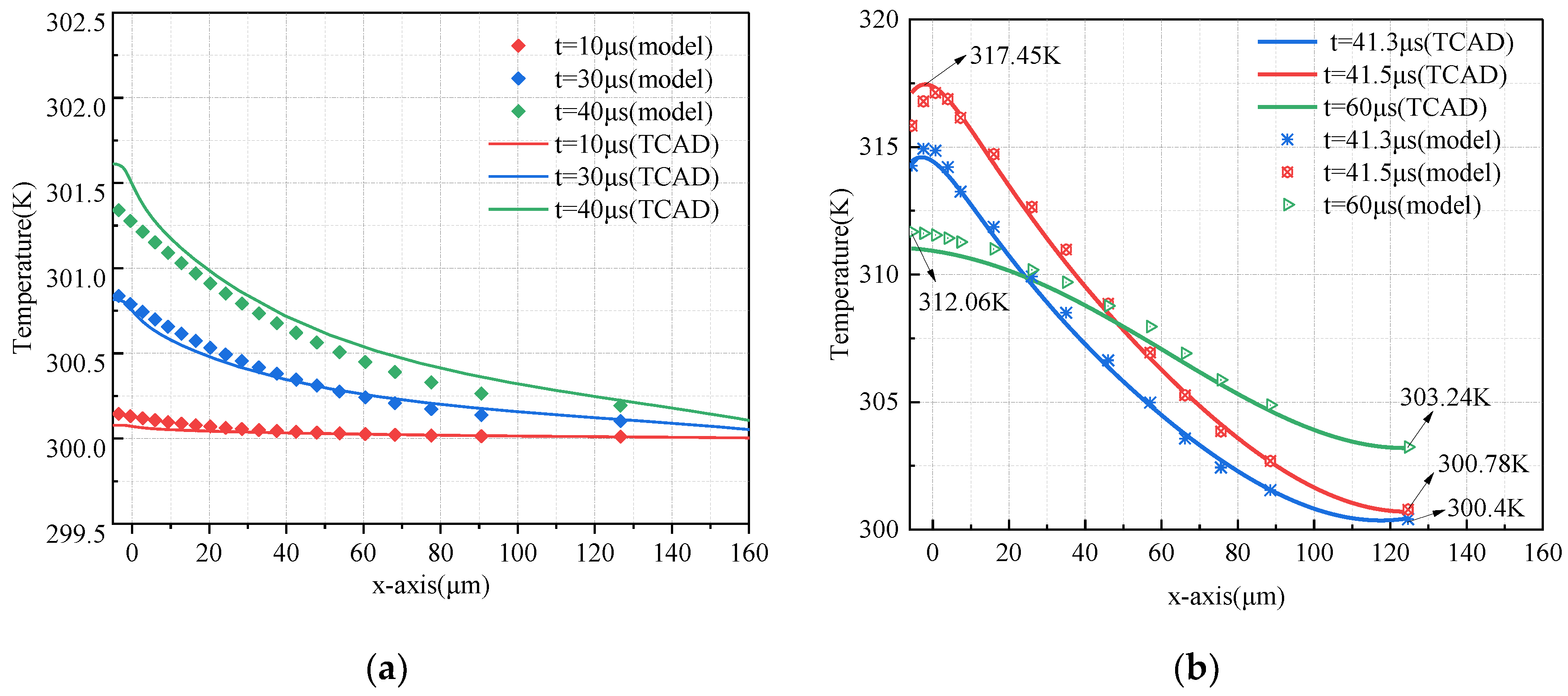
The on-state temperature distribution along the chip vertical path is shown in
Figure 8a. It can be seen that the maximum temperature distribution along the
x-axis is 1.6 °C. The temperature distribution at this point is mainly due to the unevenly distributed heat source caused by channel voltage and J
1 junction voltage.
The transient temperature distribution along the chip vertical path is shown in
Figure 8b. The moments
t = 41.3 μs,
t = 41.5 μs, and
t = 60 μs are taken for analysis. As can be seen, the maximum temperature located at the peak of the electric field is 317.45 K at
t = 41.5 μs. After the shutdown process, no heat source is generated in the chip. So, the chip’s heat conduction process reduces the chip’s temperature distribution. At
t = 60 μs, the temperature at the bottom of the chip gradually increases due to thermal conduction, while the peak temperature gradually decreases. Therefore, the temperature distribution in the entire chip drops to 8.82 °C. In addition, the highest temperature location gradually moves from the electric field’s peak to the chip’s top surface. The temperature distribution error along the chip vertical path between the two models is less than 1 °C.
4.3. Comparison of Single Time-Scale and Multi-Timescale Simulation Efficiency
To verify the computational efficiency of the proposed model, this section first compares the proposed model’s efficiency with the TCAD finite element model in evaluating temperature distribution at a single short-duration transient microsecond-scale. Secondly, using a single-phase full-bridge inverter as an example, the applicability of the proposed model evaluating the short-duration transient temperature distribution in a complex circuit system is verified. Compared with the TCAD finite elements model, the simulation efficiency of the proposed model is improved. The software runs on the same computer with an Intel(R) Core(TM) i5-8265 U CPU model.
For the comparison of the computational efficiency at a single short-duration microsecond-scale, the proposed model improves the simulation speed by more than 80 times, taking the high current shutdown conditions as examples. The double-pulse circuit parameters, simulation time, and simulation speed increase multiplier are shown in
Table 5.
The system-level circuit uses a single-phase full-bridge inverter with a bus voltage of 900 V, load resistance Rload = 0.05 Ω, load inductance Lload = 0.5 mH, and single-phase frequency doubling modulation with a carrier frequency of 50 Hz and a modulation frequency of 1 kHz. The T1 tube is chosen as the object of study, and the simulation efficiency of the T1 tube in obtaining the maximum temperature of the chip during any pulse period is studied using the TCAD model and the proposed model, respectively.
According to [
19], the electro-thermal coupling model at steady second-scale is established. The
Tvj, bus voltage, and load current of the previous pulse cycle are taken as the initial values of the short-duration transient microsecond-scale electro-thermal model, respectively. The TCAD model as well as the proposed model are simulated separately to obtain the maximum temperature of the chip in any three consecutive pulse cycles. The simulation flow chart is shown in
Figure 9. It is worth noting that the heat transfer from the chip heat to the lower layer must be considered during multiple pulse cycle times, so the influence of the solder layer, DBC layer, and substrate on the heat dissipation process needs to be considered. For the thermal network model established in this paper, the thermal resistance and thermal capacity of the remaining layers can be simply connected in series after the chip-level thermal network model using parameters from the traditional Cauer model. However, for the TCAD model, the remaining layers need to be established again, resulting in a surge in the number of meshes for the finite element model and multiplication of the simulation time. The simulation efficiencies of the two models are shown in
Table 6. As can be seen, the proposed model has more advantages in the complex circuit system coupled with multiple time scales, and the simulation efficiency is improved by 297.1 times.


