Article

A New Carrier Phase-Shift Modulation Based on Switching the Displacement Angle

1
Faculty of Electronic Engineering, Guangxi Normal University, Guilin 541000, China
2
Institute of Technology, Guilin University, Guilin 541000, China
*
Authors to whom correspondence should be addressed.
Energies 2022, 15(21), 7954; https://doi.org/10.3390/en15217954
Submission received: 27 September 2022 / Revised: 19 October 2022 / Accepted: 21 October 2022 / Published: 26 October 2022

Abstract

:
In this paper, a new carrier phase-shift (CPS) modulation method based on switching the displacement angle (SDA) is proposed to compromise the harmonic content of the output voltage and the circulating current. It can be used in medium- and low-voltage applications where the AC-side voltage and DC-side current of the modular multilevel converter (MMC) are required to have low harmonic content simultaneously. In this proposed SDA-based CPS modulation, the carrier displacement angle of the MMC with N submodules in each arm is periodically switched between the values of 0 and π/N degrees, so that the harmonic content of the output voltage and the harmonic content of the circulating current will not be in extreme conditions, which occurs when the displacement angle is set to 0 or π/N degrees. The effectiveness of this method has been verified by simulation and experimental results.

1. Introduction

With the wide application of wind power generation, photovoltaic power generation and the development of distributed generation, the application of power electronic devices such as voltage source converters (VSCs) is also increasing [1]. An MMC is one form of VSCs, and it was first proposed by R. Marquart in 2003 [2]. Compared with other VSC topologies, such as the two-level converter and three-level converter, the MMC has the advantages of better power quality and the flexible expansion of the system voltage and power level by increasing the number of submodules [3]; thus, it has become a research hotspot in the field of power electronics in recent years [4], which can be seen from its application and research in battery energy storage systems [5,6], DC ice melting [7,8], motor drives [9,10], unified power flow controllers [11,12] and solid-state transformers [13,14]. With the concept of Global Energy Interconnection proposed [15], MMCs have been more widely used in the field of flexible DC transmission by virtue of their advantages.
The modulation technology of multilevel converters has undergone a series of developments. The common ones are space vector modulation [16,17], nearest level modulation [18,19], phase-disposition level-shifted modulation [20,21], CPS modulation [22,23] and so on. Among them, CPS modulation is widely used and studied in MMC applications in the medium- and low-voltage fields because it has the advantage that when the number of MMC submodules is small, the output voltage waveform can have a high equivalent switching frequency and low harmonic distortion, and the switching frequency of each submodule can be kept consistent.
Some research has shown that the digital realization of the modulation may have a significant impact on the harmonics, e.g., [24,25]. With the deepening of CPS research, more and more attention is being paid to the harmonic content of MMCs under CPS modulation to further improve the output power quality and ensure the stability and safety of the power grid. Reference [26] analyzes the harmonic characteristics of the output voltage and the circulating current when the CPS modulation method is applied to an MMC, and theoretically obtains the value of the displacement angle to minimize the harmonic content of the output voltage or the circulating current. However, when we set the displacement angle to one of the two angles, either the output voltage or the circulating current of the MMC has a serious harmonic problem, whereas the other is relatively mild. The higher harmonics in the operation of MMCs often have a negative impact on the electrical equipment [27]. Therefore, it is necessary to make a compromise between the two to achieve performance balance. An SDA-based CPS modulation method is proposed in this paper, which realizes the compromise between the minimization of output voltage harmonics and the cancellation of circulating current harmonics.

2. Principal of CPS Modulation for MMC

2.1. Basic Topology of MMC

The basic topology of an MMC is shown in Figure 1, which contains three phases (A, B and C). Each phase includes an upper arm and a lower arm with N submodules (SM). Figure 1b can be used to represent the equivalent circuit of phase j (j = A, B, C) in the MMC, where L represents the arm inductance, uoj represents the output AC voltage of phase j, icj represents the circulating current of phase j, and all submodules of the upper and lower arms are equivalent to the AC voltage sources uuj and ulj, respectively. Since the submodule of the MMC usually adopts a half-bridge circuit, the submodule involved in this paper adopts a half-bridge circuit structure [28]. As shown by the dashed box in Figure 1a, the driving signals of the two IGBTs (S1 and S2) of the half-bridge submodule are a pair of complementary high-level and low-level signals.

2.2. CPS Modulation and Harmonic Analysis

In the CPS modulation method discussed in this paper, the driving signal of each submodule is a pair of complementary sinusoidal pulse-width modulation (SPWM) signals, which is obtained by comparing a sinusoidal reference signal whose angular frequency is ω with a triangular carrier signal whose angular frequency is ωc (its frequency is fc). Figure 2 is a schematic diagram of the CPS-PWM of the MMC. M is the modulation index. In CPS modulation, each submodule has its own corresponding triangular carrier signal. For the triangular carrier of each submodule of the same arm, there will be a phase difference of 2π/N between the former and the latter. At the same time, there is a phase difference of θ between the carriers of the submodules at the same position in the upper arm and the lower arm, which is called the carrier displacement angle.
Reference [26] analyzes the harmonic characteristics of uoj and icj in Figure 1a through CPS modulation on the premise of ignoring the low-order harmonics of the capacitor voltage and arm current. The analysis results show that:
u o j = 1 2 M U dc cos ( ω t + δ j ) + m = 1 n = ( 1 ) n 2 U dc m π N J 2 n + 1 N m ( M N m π 2 ) × cos ( N m ω c t + Q ) cos N m ( θ π ) 2
i c j = I dc 3 m = 1 n = ( 1 ) n U dc J 2 n + 1 N m ( M N m π 2 ) m π N L [ N m ω c + ( 2 n + 1 N m ) ω ] × cos ( N m ω c t + Q ) sin N m ( θ π ) 2
In the above formula, m represents the multiple of the frequency of the triangular carrier (m = 1, 2, …), and n represents the multiple of the frequency of the sinusoidal reference signal (n = …, −1, 0, 1, …). From Equations (1) and (2), it can be seen that the harmonic frequency of uoj and icj is an integral multiple of N times of the carrier frequency. If the amplitudes of each harmonic of the (Nm)th harmonic group in output voltage uoj and circulating current icj are defined as V ^ m n and I ^ m n respectively, then:
V ^ m n = K m n × | cos N m ( θ π ) 2 |
I ^ m n = H m n × | sin N m ( θ π ) 2 |
According to Equations (3) and (4), θ will have a great impact on the amplitude of harmonic components of the output voltage and the circulating current, which is deeply analyzed in reference [26].

2.3. Selection of Displacement Angle of Carrier Wave with Minimum Output Voltage Harmonic or Cancellation of Circulating Current Harmonic

According to [26], when N is odd and θ is π/N, or N is even and θ is 0, the MMC circulating current harmonic is the smallest, and at this time, the amplitude of each harmonic of each circulating current harmonic group is 0:
I ^ m n = 0
At the same time, the amplitude of each harmonic of the output voltage reaches the maximum value:
V ^ m n = K m n
when N is odd and θ is 0, or N is even and θ is π/N, the output voltage harmonic of MMC is the minimum, and the output voltage can be expressed as follows:
u o j = 1 2 M U dc cos ( ω t + δ j ) + m = 1 n = ( 1 ) N m + n U dc m π N J 2 n + 1 2 N m ( M N m π ) cos ( 2 N m ω c t + Q )
It can be seen that at this time, the frequency of the lowest harmonic group of uoj rises to 2Nfc. In this case, the even harmonic groups of both the output voltage and the circulating current are consistent with the previous case. However, all harmonics of the odd multiple harmonic groups of the output voltage are eliminated:
V ^ m n = 0 , m = 1 , 3 , 5
and each harmonic amplitude of the odd multiple harmonic group of the circulating current reaches the maximum value:
I ^ m n = H m n , m = 1 , 3 , 5

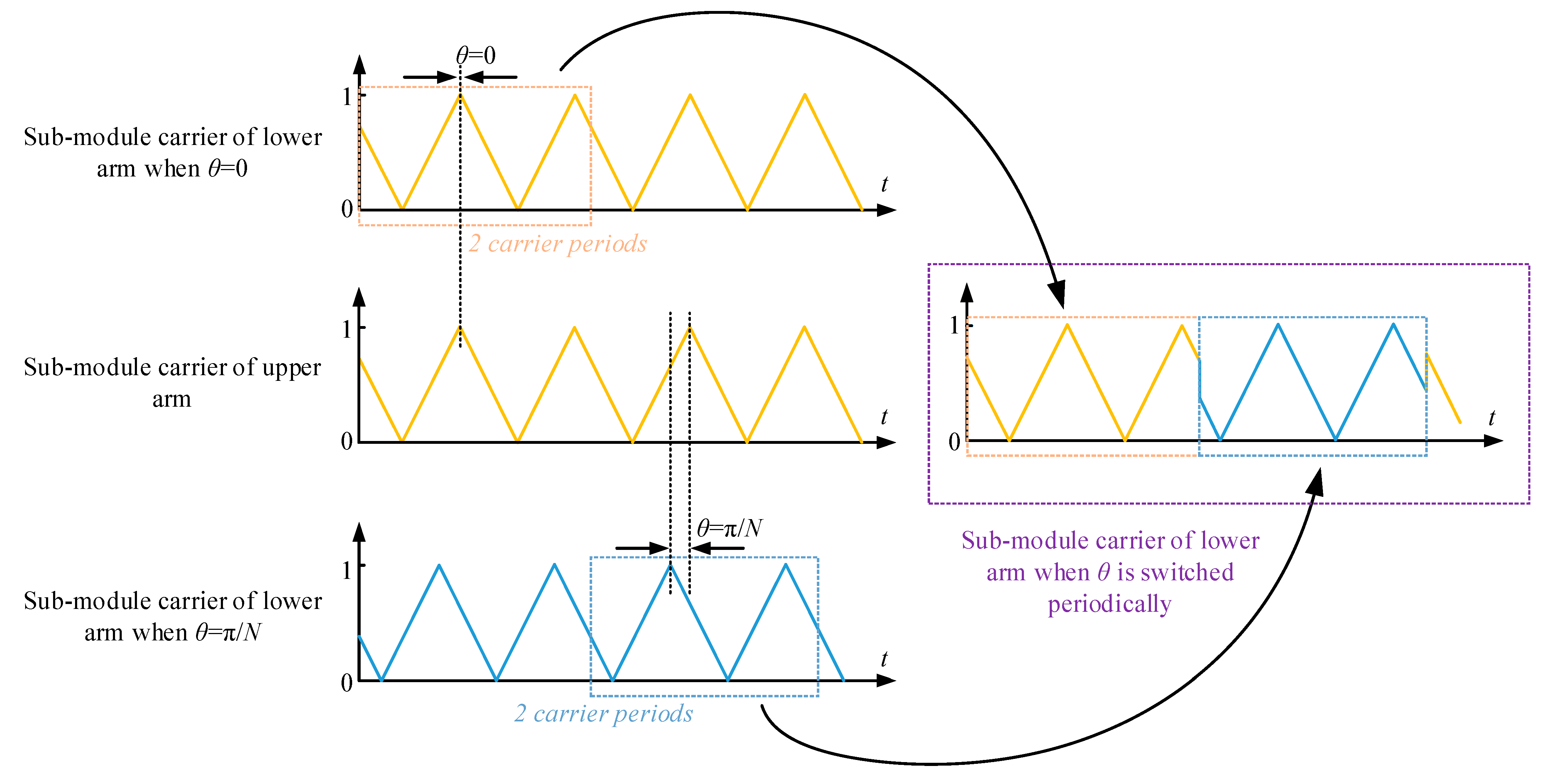
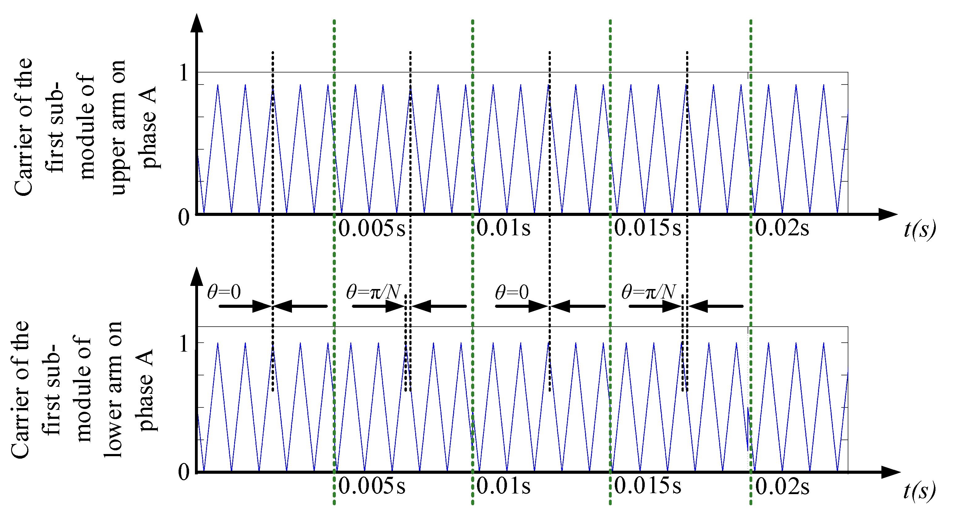
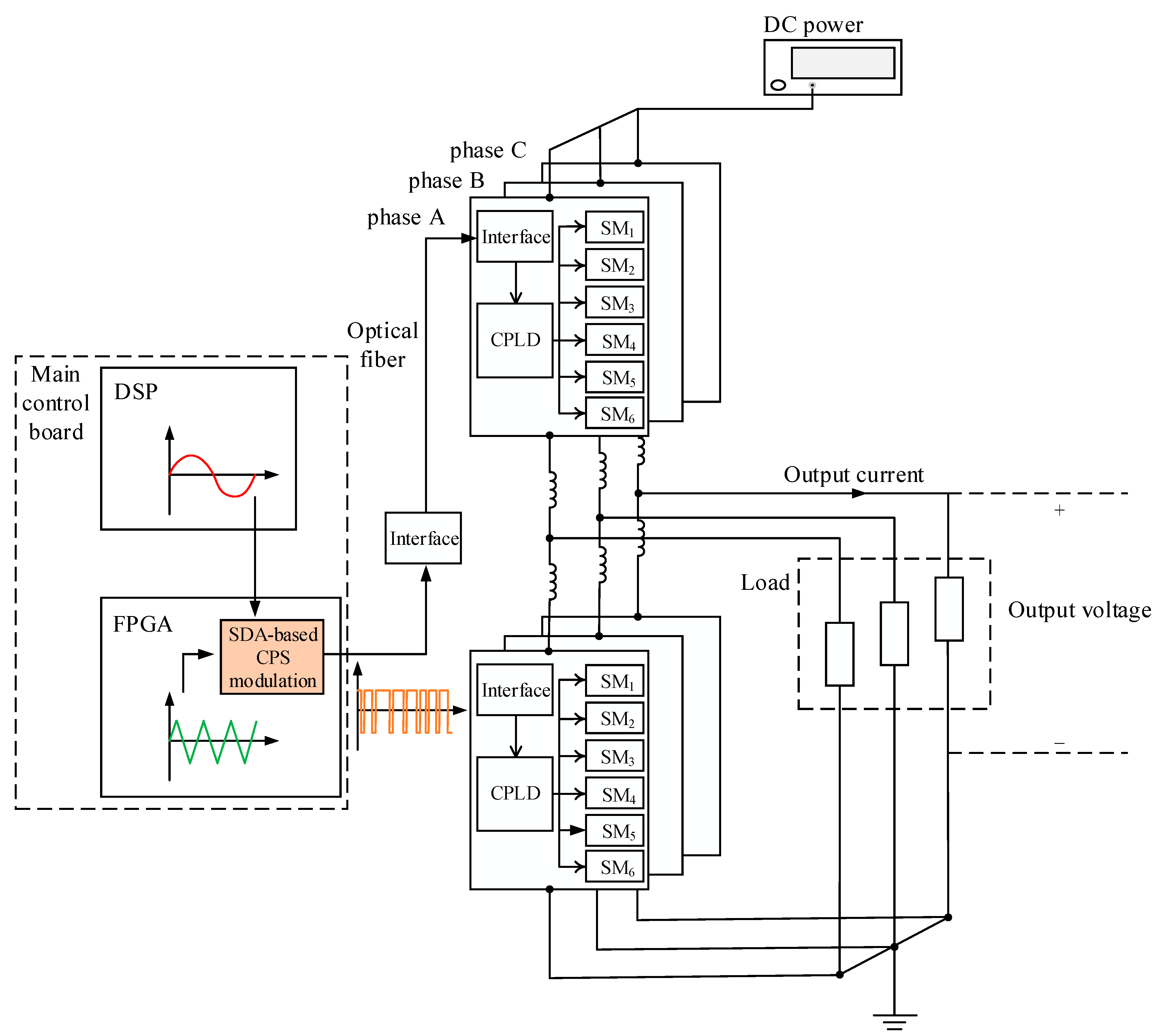
3. SDA-Based CPS Modulation

According to Section 2, we know that no matter if θ is 0 or π/N, there is always one harmonic characteristic between the output voltage and the circulating current that is the best and one that is the worst. If we do not want the output voltage or the circulating current to have the worst harmonic characteristics, we can change θ periodically between two fixed values. This is called SDA-based CPS modulation. We can define the switching period of θ as an integer multiple of the period of the carrier, and the multiple is defined as n. In Figure 3, the triangular carrier of a submodule in the lower arm is taken as an example to visually describe the time-domain performance of the carrier when SDA-based CPS modulation is adopted. On the left side of Figure 3, the waveform in the middle represents the carrier of the upper arm’s submodule, and the upper and lower parts of it are the carriers of the lower arm’s submodule when θ = 0 and θ = π/N. The waveform on the right side of Figure 3 is the carrier of the lower arm’s submodule when θ is switched periodically. When the displacement angle is switched periodically, the displacement angle of the first and second periods of the carrier is 0. At the end of the second carrier period, since the displacement angle is switched from 0 to π/N, the lower-arm triangular carrier waveform will quickly advance the original phase by π/N while continuing to maintain two carrier periods, and then the displacement angle will return to 0. The above process will be repeated continuously.
Based on the conclusion in Section 2, at this time, the even harmonic group amplitudes of the output voltage and the circulating current are at the maximum and minimum values, respectively, whereas their odd harmonic group amplitudes will be compromised between the maximum and minimum values:
0 < I ^ m n < H m n ,   m = 1 , 3 , 5
0 < V ^ m n < K m n ,   m = 1 , 3 , 5
It can be seen that the amplitude of each harmonic of all odd times of harmonic groups of the output voltage and the circulating current will not be the worst case. According to [26], the DC-side current and circulating current have the following relationship:
i dc = j = a , b , c i c j
Therefore, this method realizes the balanced regulation of the DC-side current quality and the AC-side voltage quality.

4. Simulation Result

4.1. Simulation Platform and Relevant Parameters

In order to verify the effect of the method described in Section 3, a simulation model of the MMC is built with the MATLAB/Simulink platform, and the time-domain waveform and spectrum diagram of the output voltage and the circulating current under the conditions of θ = 0, θ = π/N and SDA-based CPS modulation being adopted are analyzed. The specific parameters of the MMC simulation model are shown in Table 1.

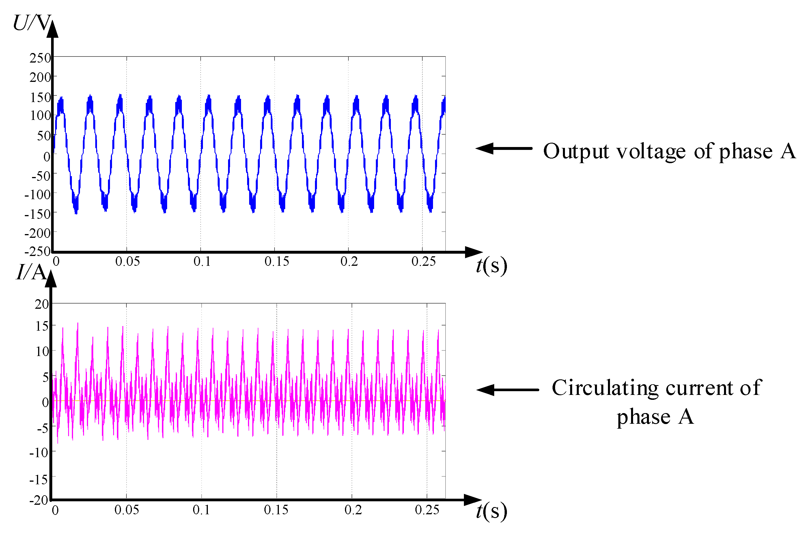
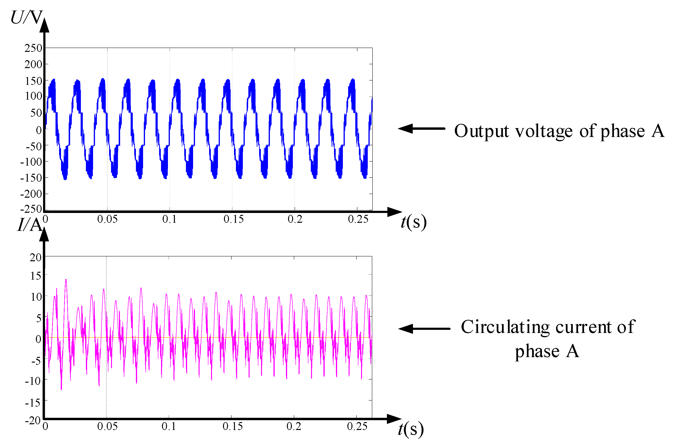
4.2. Comparative Experiment with Simulation

When the traditional CPS modulation method is applied, the carrier displacement angle is usually fixed at 0 or π/N degrees [29,30,31]. In this section, the effect of SDA-based CPS modulation is analyzed, and compared with the traditional CPS modulation method that fixes the carrier displacement angle to be above two specific angles.
First, the triangular carriers in the above three cases should be generated. Figure 4 shows a comparison diagram of the triangular carrier of the first submodule of the upper arm and the triangular carrier of the first submodule of the lower arm of phase A in the case of SDA-based CPS modulation being adopted, where θ is switched every five triangular carrier periods (n = 5). As can be seen from Figure 4, in the first to fifth carrier periods, θ is 0. At the end of the fifth carrier period, since θ is switched from 0 to π/N, the waveform will be ahead of the original phase by π/N, and will continue to maintain five carrier periods; then, θ will return to 0. This process will be repeated continuously. Compare the carrier wave when θ = 0, θ = π/N and SDA-based CPS modulation is adopted with the reference signal to obtain the switch drive signal of each submodule, and generate the output voltage and the circulating current of phase A in the above three cases, as shown in Figure 5, Figure 6 and Figure 7, respectively.
As shown in Figure 5, when the output voltage harmonics are eliminated, the higher-order harmonics of the circulating current are obvious. When the circulating current harmonic is minimized, as shown in Figure 6, the circulating current is significantly smoother, but the output voltage is rougher than that in Figure 5. In Figure 7, the circulating current is obviously characterized by half being smoother and the other half containing more high-order harmonics. The circulating current is smoother when θ = π/N, and has more burrs when θ = 0. In Figure 7, the roughness of the output voltage is between that of Figure 5 and Figure 6.
Figure 8a–c shows the frequency spectrums of the circulating current and the output voltage of phase A in the case of θ = π/N, θ = 0 and SDA-based CPS modulation being adopted, respectively. As can be seen from Figure 8b, under the condition of output harmonic elimination, the output voltage has a peak with a maximum amplitude of about 7 V at the frequency 2Nfc (6000 Hz), whereas the circulating current has a peak with a maximum amplitude of about 1.2 A at the frequency Nfc (3000 Hz). As can be seen from Figure 8a, under the condition of the circulating current harmonic cancellation, the output voltage has a peak with a maximum amplitude of 21 V at frequency Nfc, whereas the amplitude at each frequency point of the circulating current is very small. As can be seen from Figure 8c, in the case of SDA-based CPS modulation being adopted, the output voltage has a peak with a maximum amplitude of 14 V at frequency Nfc, whereas the amplitude and density of the spectrum near that frequency point are less than θ = π/N and bigger than θ = 0. The circulating current has a peak with a maximum amplitude of 0.9 A at the frequency Nfc, whereas the amplitude and density near this frequency point are less than θ = 0 and bigger than θ = π/N. The simulation results are consistent with the expression of Equations (10) and (11) and meet the expected results. In order to demonstrate whether n will affect the conclusion, this paper uses the simulation platform to test the maximum amplitude of the circulating current and the output voltage near the frequency Nfc of phase A when n is changed from 1 to 9, as shown in Table 2.
From Table 2, we can see that when n is different, the maximum amplitude of the circulating current and the output voltage near frequency Nfc of phase A will also be different, but the simulation results are consistent with the description of Equations (10) and (11).

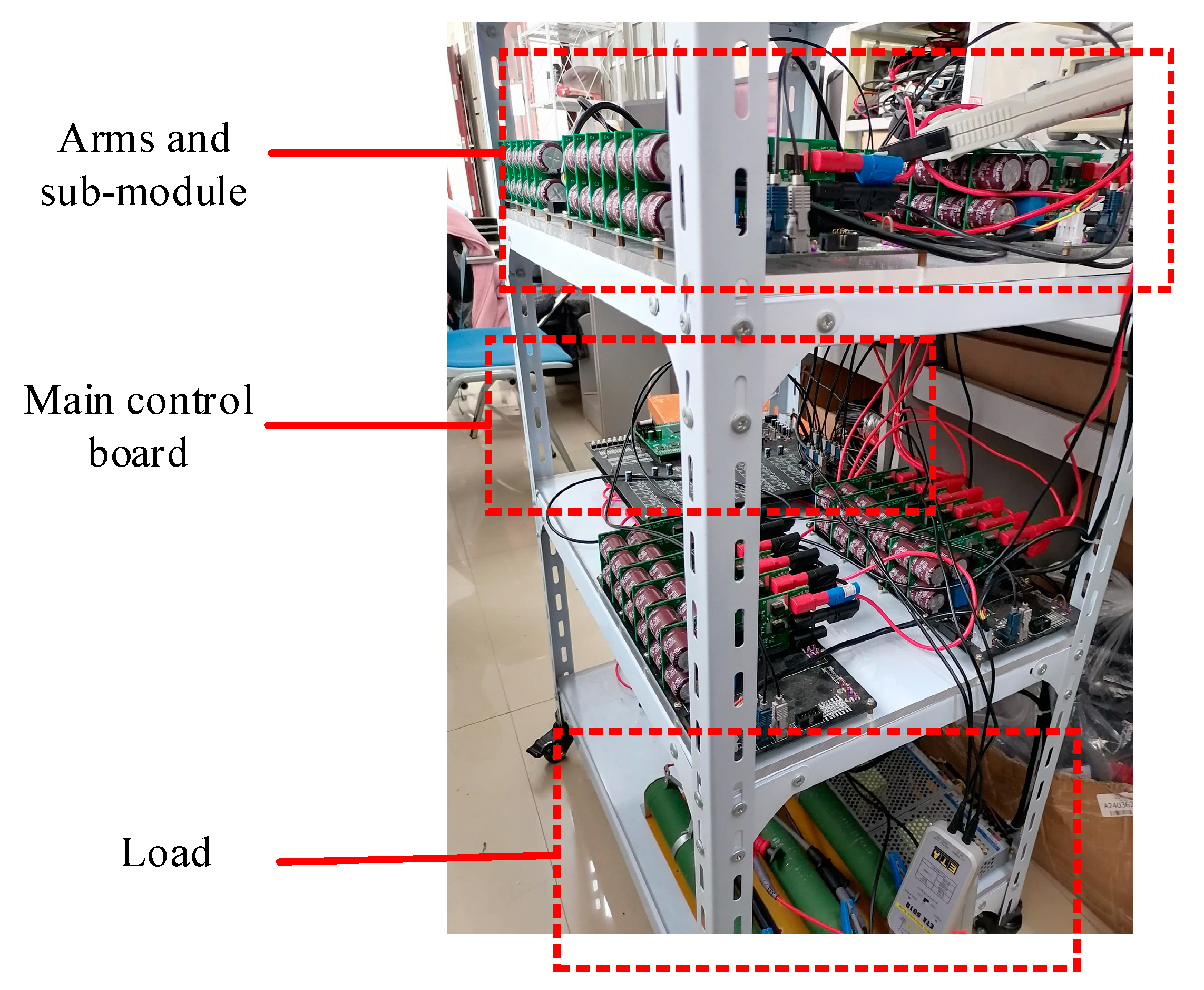
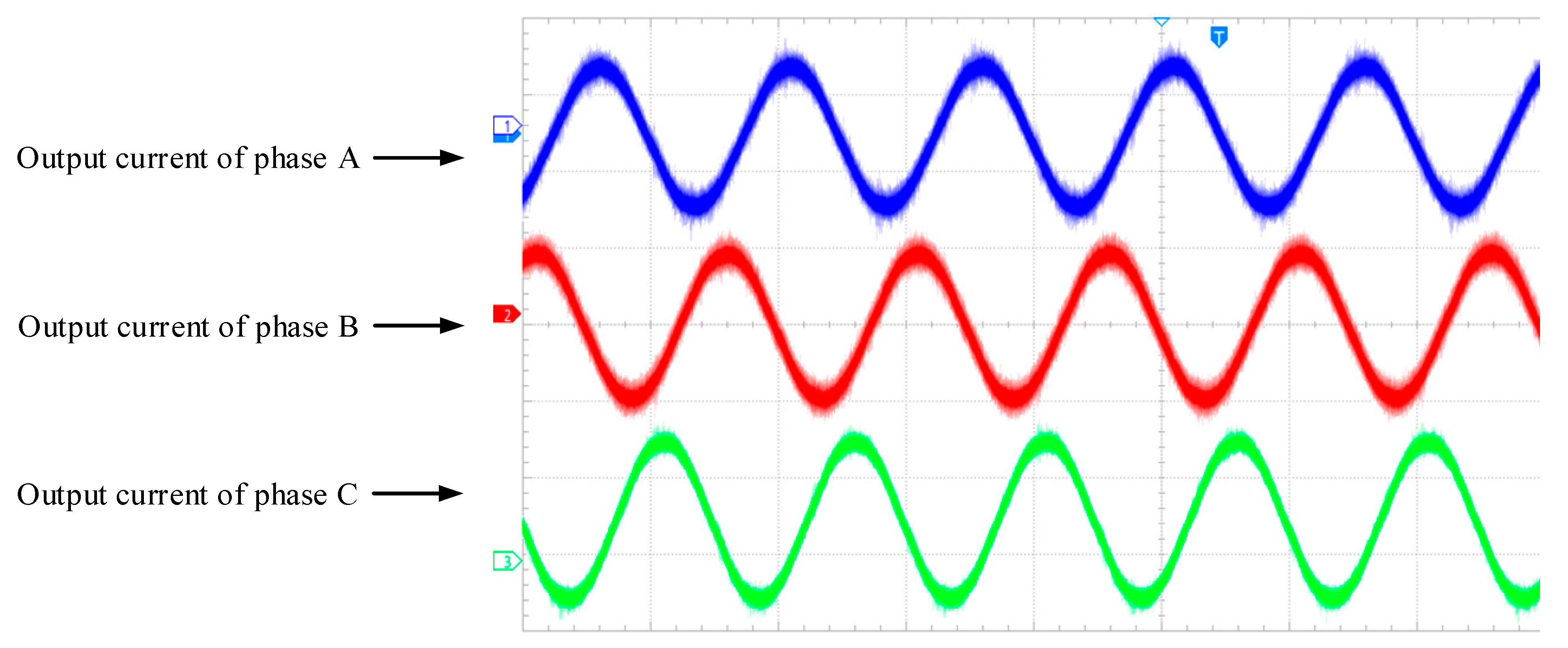
5. Verification with MMC Prototype

Considering the advantages and disadvantages of DSP and FPGA [32], an MMC experimental platform based on DSP-FPGA is built, and the feasibility of the method described in Section 3 is further verified by using the experimental platform. The main structure of the experimental platform is shown in Figure 9. The left side of Figure 9 is the main control board, which mainly includes DSP and FPGA. In this experiment, DSP is mainly responsible for the generation and adjustment of the reference signal, whereas FPGA is mainly responsible for the generation of carrier and SDA-based CPS modulation. The right side of Figure 9 is the main part of the MMC system, which consists of three phases, including the upper arm and the lower arm. Each arm contains six submodules. The PWM signal generated by the modulation will be transmitted to each arm through optical fiber communication, and then, the CPLD on each arm will analyze the signal and control the six submodules on the arm. The load adopts the star connection method, and the load resistance connected to the output of each phase is 22 Ω. The experiment was conducted under 60 V DC voltage. The MMC experimental prototype is shown in Figure 10.
When SDA-based CPS modulation is adopted, the output voltage and output current of the three phases of the MMC are shown in Figure 11 and Figure 12, respectively. It can be seen that the MMC can operate normally and stably when using the above modulation methods.
Figure 13a–c shows the frequency spectrums of the output voltage and the circulating current of phase A in the case of θ = 0, θ = π/N and SDA-based CPS modulation being adopted (take n = 6 as an example), respectively.
Through a comparison, it can be found that when SDA-based CPS modulation is adopted, the maximum amplitudes of the output voltage and the circulating current near the frequency Nfc are between the two cases of θ = 0 and θ = π/N, which is consistent with the expected conclusion.
According to Equation (12), the harmonic content of the circulating current will affect the harmonic content of the DC-side current. Figure 14a–c shows the frequency spectrums of the DC-side current in the case of θ = 0, θ = π/N and SDA-based CPS modulation being adopted, respectively. As shown in Figure 14, when SDA-based CPS modulation is adopted, the frequency spectrum of the DC-side current is consistent with that of the circulating current, which further proves that the method realizes the balanced regulation of DC-side current quality and AC-side voltage quality.

6. Conclusions

In this paper, a new SDA-based CPS modulation that achieves a compromise between the output voltage harmonic content and the circulating current harmonic content is proposed. Compared with the existing methods, this method realizes the balanced regulation of the DC-side current quality and the AC-side voltage quality, which is conducive to avoiding the risks brought to the power grid by the high-frequency harmonic content of the DC-side current or AC-side voltage of an MMC, and ensures the stability and safety of the power grid. It is especially suitable for the medium- and low-voltage application scenarios where both the DC-side current and the AC-side voltage require low harmonic content. A simulation and experiments verify the effectiveness and feasibility of this method.

Author Contributions

Conceptualization, Z.L.; methodology, Y.C. and Z.L.; software, Y.C.; validation, Y.C., D.L. (Dong Lin) and D.L. (Dan Luo); formal analysis, Z.L. and D.L. (Dan Luo); investigation, Y.C. and Z.L.; resources, S.S. and Z.L.; writing—original draft preparation, Y.C.; writing—review and editing, Z.L. and S.S.; visualization, Y.C. and D.L. (Dong Lin); supervision, S.S., Z.L. and D.W.; project administration, S.S.; funding acquisition, S.S. All authors have read and agreed to the published version of the manuscript.

Funding

This paper is supported by the National Natural Science Foundation of China (Grant No. 62061006); the Guangxi University Young and Middle-aged Teachers’ Scientific Research Basic Ability Improvement Project Support (2022KY1574); the Technology Major Project of Guangxi (AA20161002-2); and the Natural Science Foundation of Guangxi under Grant 2021JJA170004.

Data Availability Statement

Not applicable.

Conflicts of Interest

The authors declare no conflict of interest.

References

  1. Yan, Z.; Xue-Hao, H.; Guang-Fu, T.; Zhi-Yuan, H. A study on MMC model and its current control strategies. In Proceedings of the 2nd International Symposium on Power Electronics for Distributed Generation Systems, Hefei, China, 16–18 June 2010; pp. 259–264. [Google Scholar]
  2. Lesnicar, A.; Marquardt, R. An innovative modular multilevel converter topology suitable for a wide power range. In Proceedings of the 2003 IEEE Bologna Power Tech Conference Proceedings, Bologna, Italy, 23–26 June 2003; Volume 2, p. 6. [Google Scholar]
  3. Zhang, L.; Zou, Y.; Yu, J.; Qin, J.; Vittal, V.; Karady, G.G.; Shi, D.; Wang, Z. Modeling, control, and protection of modular multilevel converter-based multi-terminal HVDC systems: A review. CSEE J. Power Energy Syst. 2017, 3, 340–352. [Google Scholar] [CrossRef]
  4. Sun, T.; Pei, X. Comparison Analysis on EMI Sources of MMC Under NLM and CPS-PWM Strategies. In Proceedings of the 2019 4th IEEE Workshop on the Electronic Grid (eGRID), Xiamen, China, 11–14 November 2019; pp. 1–4. [Google Scholar]
  5. Li, N.; Gao, F.; Hao, T.; Ma, Z.; Zhang, C. SOH Balancing Control Method for the MMC Battery Energy Storage System. IEEE Trans. Ind. Electron. 2018, 65, 6581–6591. [Google Scholar] [CrossRef]
  6. Bayat, H.; Yazdani, A. A Hybrid MMC-Based Photovoltaic and Battery Energy Storage System. IEEE Power Energy Technol. Syst. J. 2019, 6, 32–40. [Google Scholar] [CrossRef]
  7. Guobang, B.; Wei, N.; Lusong, Z.; Wenyong, Y.; Jianwen, L.; Xiaotang, M. SVG control function and realization of modular multi-level DC ice melting device. In Proceedings of the 2021 IEEE 16th Conference on Industrial Electronics and Applications (ICIEA), Chengdu, China, 1–4 August 2021; pp. 1261–1266. [Google Scholar]
  8. Guobang, B.; Xiaohong, M.; Yangzeyu, O.; Li, L.; Jianwen, L.; Binyuan, W. Research on Influencing Factors of voltage control for MMC type mobile DC ice melting device. In Proceedings of the 2021 IEEE 16th Conference on Industrial Electronics and Applications (ICIEA), Chengdu, China, 1–4 August 2021; pp. 1256–1260. [Google Scholar]
  9. Elserougi, A.A.; Abdel-Khalik, A.S.; Massoud, A.M.; Ahmed, S. An asymmetrical six-phase induction motor drive based on nine-arm Modular Multilevel Converter (9AMMC) with circulating current suppression. In Proceedings of the 2015 4th International Conference on Electric Power and Energy Conversion Systems (EPECS), Sharjah, United Arab Emirates, 24–26 November 2015; pp. 1–6. [Google Scholar]
  10. Zhao, F.; Xiao, G.; Yang, D.; Wu, Z.; Meng, X. A Flexible Reduced Capacitor Voltages Strategy for Variable-Speed Drives with Modular Multilevel Converter. In Proceedings of the 2018 International Power Electronics Conference (IPEC-Niigata 2018 -ECCE Asia), Niigata, Japan, 20–24 May 2018; pp. 1549–1553. [Google Scholar]
  11. Zhou, Y.; Jiang, D.Z.; Yin, R.; Liang, Y.Q. An improved topology of Unified Power Flow Controller based on MMC with Fault Current Limiting. In Proceedings of the 8th IET International Conference on Power Electronics, Machines and Drives (PEMD 2016), Glasgow, UK, 19–21 April 2016; pp. 1–6. [Google Scholar]
  12. Hao, Q.; Man, J.; Gao, F.; Guan, M. Voltage Limit Control of Modular Multilevel Converter Based Unified Power Flow Controller Under Unbalanced Grid Conditions. IEEE Trans. Power Deliv. 2018, 33, 1319–1327. [Google Scholar] [CrossRef]
  13. LI, Y.; LIU, C.; CAI, X. A Developed Dual MMC Isolated DC Solid State Transformer and Its Modulation Strategy. In Proceedings of the 2018 International Power Electronics Conference (IPEC-Niigata 2018 -ECCE Asia), Niigata, Japan, 20–24 May 2018; pp. 2245–2249. [Google Scholar]
  14. Zheng, G.; Chen, Y.; Kang, Y. A Modular Multilevel Converter (MMC) Based Solid-State Transformer (SST) Topology With Simplified Energy Conversion Process and Magnetic Integration. IEEE Trans. Ind. Electron. 2021, 68, 7725–7735. [Google Scholar] [CrossRef]
  15. Feng, L.; Xu, X.; Wang, W.; Wang, L.; Zhang, H.; Li, W.; Zhang, Y. The design and implementation of global energy interconnection digital research platform. In Proceedings of the 2017 IEEE Conference on Energy Internet and Energy System Integration (EI2), Beijing, China, 26–28 November 2017; pp. 1–5. [Google Scholar]
  16. Deng, Y.; Wang, Y.; Teo, K.H.; Harley, R.G. A Simplified Space Vector Modulation Scheme for Multilevel Converters. IEEE Trans. Power Electron. 2016, 31, 1873–1886. [Google Scholar] [CrossRef]
  17. Sharma, V.K.; Anand, V.; Vaish, V.; Bharti, R. A new control scheme for modular converters. In Proceedings of the 2015 57th International Symposium ELMAR (ELMAR), Zadar, Croatia, 28–30 September 2015; pp. 137–140. [Google Scholar]
  18. Hu, P.; Jiang, D. A Level-Increased Nearest Level Modulation Method for Modular Multilevel Converters. IEEE Trans. Power Electron. 2015, 30, 1836–1842. [Google Scholar] [CrossRef]
  19. Liu, H.; Zhang, C.; Xu, L.; Sun, X.; Gu, S.; Li, X. Voltage Balancing Control Strategy for MMC Based on NLM Algorithm. In Proceedings of the 2019 14th IEEE Conference on Industrial Electronics and Applications (ICIEA), Xi’an, China, 19–21 June 2019; pp. 1075–1079. [Google Scholar]
  20. Mei, J.; Shen, K.; Xiao, B.; Tolbert, L.M.; Zheng, J. A New Selective Loop Bias Mapping Phase Disposition PWM With Dynamic Voltage Balance Capability for Modular Multilevel Converter. IEEE Trans. Ind. Electron. 2014, 61, 798–807. [Google Scholar] [CrossRef]
  21. McGrath, B.P.; Teixeira, C.A.; Holmes, D.G. Optimized Phase Disposition (PD) Modulation of a Modular Multilevel Converter. IEEE Trans. Ind. Appl. 2017, 53, 4624–4633. [Google Scholar] [CrossRef]
  22. Zhang, H.; Meng, Y.; Wang, X.; Zou, Y.; Wu, X.; Liu, C.; Zhou, Q.; Zhu, W. An improved CPS-SPWM and unified modulation strategy for multilevel converter. In Proceedings of the 2016 IEEE PES Asia-Pacific Power and Energy Engineering Conference (APPEEC), Xi’an, China, 25–28 October 2016; pp. 1306–1310. [Google Scholar]
  23. Bashir, S.B.; Zidan, H.A.; Memon, Z.A. A Modified CPS-PWM for Capacitor Voltage Ripples Reduction of Modular Multilevel Converter Based Variable Speed Drive. In Proceedings of the 2020 IEEE 29th International Symposium on Industrial Electronics (ISIE), Delft, The Netherlands, 17–19 June 2020; pp. 601–605. [Google Scholar]
  24. Yang, J.; Liu, J.; Shi, Y.; Zhao, N.; Zhang, J.; Fu, L.; Zheng, T.Q. Carrier-Based Digital PWM and Multirate Technique of a Cascaded H-Bridge Converter for Power Electronic Traction Transformers. IEEE J. Emerg. Sel. Top. Power Electron. 2019, 7, 1207–1223. [Google Scholar] [CrossRef]
  25. He, S.; Zhou, D.; Wang, X.; Zhao, Z.; Blaabjerg, F. A Review of Multisampling Techniques in Power Electronics Applications. IEEE Trans. Power Electron. 2022, 37, 10514–10533. [Google Scholar] [CrossRef]
  26. Li, B.; Yang, R.; Xu, D.; Wang, G.; Wang, W.; Xu, D. Analysis of the Phase-Shifted Carrier Modulation for Modular Multilevel Converters. IEEE Trans. Power Electron. 2015, 30, 297–310. [Google Scholar] [CrossRef]
  27. Yang, S.; Shao, Z.; Zheng, W.; Chen, F. Mitigation of Background Harmonics Effect on MMC Controller Based on a Novel Coordinate Transformation Technique. IEEE Access 2019, 7, 167113–167126. [Google Scholar] [CrossRef]
  28. Lu, S.; Yuan, L.; Li, K.; Zhao, Z. An Improved Phase-Shifted Carrier Modulation Scheme for a Hybrid Modular Multilevel Converter. IEEE Trans. Power Electron. 2017, 32, 81–97. [Google Scholar] [CrossRef]
  29. Wang, H.; Yang, S.; Chen, H.; Feng, X.; Blaabjerg, F. Synchronization for an MMC Distributed Control System Considering Disturbances Introduced by Submodule Asynchrony. IEEE Trans. Power Electron. 2020, 35, 12834–12845. [Google Scholar] [CrossRef]
  30. Sha, G.; Duan, Q.; Sheng, W.; Ma, C.; Zhao, C.; Zhang, Y.; Tian, J. Research on Multi-Port DC-DC Converter Based on Modular Multilevel Converter and Cascaded H Bridges for MVDC Applications. IEEE Access 2021, 9, 95006–95022. [Google Scholar] [CrossRef]
  31. Gauttam, G.; Hrishikesan, V.M.; Kumar, C. Single Phase Modular Multilevel Converter for Photovoltaic Application. In Proceedings of the 2022 4th International Conference on Energy, Power and Environment (ICEPE), Shillong, India, 29 April–1 May 2022; pp. 1–6. [Google Scholar]
  32. Koleff, L.; Conde, M.; Hayashi, P.; Sacco, F.; Enomoto, K.; Pellini, E.; Komatsu, W.; Matakas, L. Development of a FPGA-Based Control System for Modular Multilevel Converter Applications. In Proceedings of the 2019 IEEE 15th Brazilian Power Electronics Conference and 5th IEEE Southern Power Electronics Conference (COBEP/SPEC), Santos, Brazil, 1–4 December 2019; pp. 1–6. [Google Scholar]
Figure 1. (a) Basic topology of MMC and (b) equivalent circuit of phase j.
Energies 15 07954 g001
Figure 2. CPS-PWM of MMC.
Energies 15 07954 g002
Figure 3. CPS-PWM schematic diagram when SDA-based CPS modulation is adopted.
Energies 15 07954 g003
Figure 4. Comparison diagram of upper- and lower-arm carriers when SDA-based CPS modulation is adopted.
Energies 15 07954 g004
Figure 5. Waveform of the output voltage and the circulating current of phase A when θ = 0.
Energies 15 07954 g005
Figure 6. Waveform of the output voltage and the circulating current of phase A when θ = π/N.
Energies 15 07954 g006
Figure 7. Waveform of the output voltage and the circulating current of phase A when SDA-based CPS modulation is adopted.
Energies 15 07954 g007
Figure 8. Frequency spectrum of the output voltage and the circulating current when (a) θ = π/N, (b) θ = 0 or (c) SDA-based CPS modulation is adopted.
Energies 15 07954 g008
Figure 9. Main structure diagram of MMC experimental platform.
Energies 15 07954 g009
Figure 10. MMC experimental prototype based on DSP-FPGA.
Energies 15 07954 g010
Figure 11. Waveform of output voltage of three phases of MMC.
Energies 15 07954 g011
Figure 12. Waveform of output current of three phases of MMC.
Energies 15 07954 g012
Figure 13. Experimental frequency spectrum of the output voltage and the circulating current when (a) θ = 0, (b) θ = π/N or (c) SDA-based CPS modulation is adopted.
Energies 15 07954 g013
Figure 14. Experimental frequency spectrum of DC-side current when (a) θ = 0, (b) θ = π/N or (c) SDA-based CPS modulation is adopted.
Energies 15 07954 g014
Table 1. Parameter table of MMC simulation model.
Parameter NameParameter Value
Number of submodules on one arm3
DC voltage300 V
Reference voltage frequency50 Hz
Rated voltage of submodule100 V
Capacitance of submodule0.001867 F
Arm inductance0.0008 H
Triangular carrier frequency1000 Hz
Modulation index0.87
Table 2. The maximum amplitude of the circulating current and the output voltage near frequency Nfc change with θ.
θThe Maximum Amplitude of the Circulating Current Near Frequency NfcThe Maximum Amplitude of the Output Voltage Near Frequency Nfc
θ = 01.2 A1.5 V
θ = π/N0.005 A21 V
n = 10.6 A10.5 V
n = 20.6 A12 V
n = 30.6 A9.55 V
n = 40.6 A11.6 V
n = 50.9 A14 V
n = 60.6 A10.5 V
n = 70.6 A9.8 V
n = 80.6 A10.5 V
n = 90.6 A10.5 V
Publisher’s Note: MDPI stays neutral with regard to jurisdictional claims in published maps and institutional affiliations.

