Article

Performance Analysis and Evaluation of Multiphase Split-Source Inverters

by
Sherif M. Dabour
1,2,*,
Ahmed A. Aboushady
2,
I. A. Gowaid
2,3,
Mohamed. A. Elgenedy
2 and
Mohamed E. Farrag
2
1
Department of Electrical Power and Machines Engineering, Faculty of Engineering, Tanta University, Tanta 31733, Egypt
2
Electrical Power Engineering Department, School of Computing, Engineering and Built Environment, Glasgow Caledonian University, Glasgow G4 0BA, UK
3
Electrical Engineering Department, Faculty of Engineering, Alexandria University, Alexandria 21544, Egypt
*
Author to whom correspondence should be addressed.
Energies 2022, 15(22), 8411; https://doi.org/10.3390/en15228411
Submission received: 16 October 2022 / Revised: 7 November 2022 / Accepted: 7 November 2022 / Published: 10 November 2022
(This article belongs to the Topic Power Converters)

Abstract

:
Due to their many advantages over their counterparts, such as Z-source inverters (ZSIs), split-source inverters (SSIs) have recently received much attention as single-stage boost inverters. This paper discusses a multiphase version of the SSI topology for the first time. Among multiphase systems undergoing a revolution in the research area, five-phase motor drives are a relatively practical selection in industrial applications. Therefore, this paper focuses on a five-phase SSI as an example. The topology, operating principles, modulation techniques, and performance analysis of the analyzed topology are introduced. A modified space-vector modulation (MSVM) scheme is developed to eliminate low-frequency ripples in the input current. There is also a detailed analysis and graphical evaluation of the output currents ripples using the space-vector approach. It is evident that multiphase SSI is suitable for motor drives, especially when a high-output voltage gain is required. In addition to having a nearly identical ripple in output current to a conventional VSI, it has the benefit of performing the boosting action in a single stage with fewer passive components and a low ripple in input current. Finally, the simulation and experimental results have been conducted to demonstrate the viability of the multiphase SSI studied in the theoretical study and analysis.

1. Introduction

Recently, multiphase (more than three-phase) machines have begun to replace their conventional AC counterparts because of their high reliability, inherent torque ripple reduction, and resulting reduced power electronic devices required for operation [1]. As a result of these advantages, they are great candidates for a variety of critical applications, including variable speed drives (VSDs), wind energy, and ship propulsion [1,2]. Amongst multiphase machines, the five-phase motor may produce the lowest copper loss and total loss [3]. In most cases, voltage source (VSIs) or current source inverters (CSIs), along with matrix converters (MCs), are employed as power supplies for five-phase motor drives, as shown in Figure 1 [4,5,6].
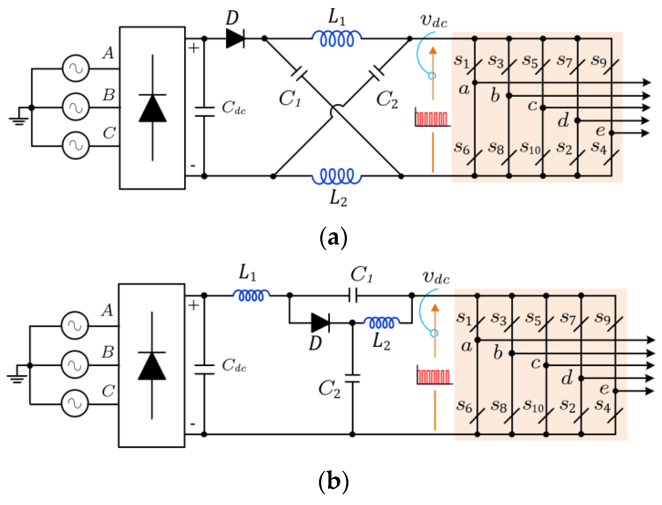
As VSIs and matrix converters only operate in bucking mode, additional circuits are required to increase voltage gain [4,6]. As a result, these circuits increase the cost of the system and reduce its overall efficiency [5]. CSIs operate in boosting mode, but this is complex to implement and requires more passive components [5]. As a result of their superior performance in terms of system complexity, size, weight, and the ability to perform both bucking and boosting actions, single-stage topologies have replaced conventional architectures. Five-phase Z- and quasi-Z-source inverters (ZSI/qZSI), shown in Figure 2, have been gaining increasing attention in recent years [7,8]. This overcomes the conceptual and theoretical shortcomings of the traditional VSIs and CSIs. Compared to VSD systems that are based on VSIs and CSIs, the ZSI offers additional advantages [9,10]:
-
Regardless of the input voltage, the voltage gain, G , can be improved by producing any desired AC output voltage, even that greater than the line voltage.
-
No additional circuits are needed to provide ride-through during voltage sags.
-
This reduces the line’s common-mode voltage and harmonic current while improving the power factor.
Many publications discuss the modulation techniques of ZSIs for the different number of phases and different applications [11,12,13,14]. It can be mainly classified into three methods: (1) simple-boost (SB), (2) maximum-constant-boost (MCB), and (3) maximum-boost (MB) control methods. The SB control scheme produces lower voltage gains than the MB control scheme. Meanwhile, the MB method requires more passive elements in the impedance network because the shoot-through (ST) duty ratio periodically varies. Furthermore, this variation increases the peak inductor current and capacitor voltage. An improved maximum-constant boost (MCB) modulation method obtains constant ST variation with a higher boosting factor than SB modulation. Despite the merits of multiphase ZSIs, their output voltage magnitude varies accurately in a narrow range by controlling the shoot-through (ST) duty ratio.
Recently, the split-source inverter (SSI) represents an alternative to the basic ZSI and qZSI topologies. It has been first invented by [15] for a single-phase system and developed in [16] for the three-phase topology, as shown in Figure 3. The potential advantages of SSI over ZSI can be summarized as follows [9]:
It has a continuous input current and DC-link voltage.
It has lower voltage stresses across the switches for high-voltage gains.
It requires a lower passive component count.
It uses the same switching states as the VSI, which uses a different state for ST.
Compared with the two-stage architecture, no additional active switch is required in the SSI.
Several topologies have been developed with the idea of the basic SSI to achieve higher boosting capabilities [17,18,19], multilevel technologies [20,21,22], and multiport output inverters [23,24]. Although the reduction in the number of switch counts and passive elements in these architectures leads to a reduction in the volume and weight of the inverters, it suffers from some demerits, such as rapid commutations for the input diodes and higher current stresses for the lower switches [16,19]. The authors of this paper, however, have not conducted any extensive research to explore and extend the concept of basic SSI to multiphase systems based on their best knowledge. Therefore, this paper aims to fill this gap in the multiphase drive architecture by extending the basic SSI to n-phase designs. A five-phase SSI topology is fully explored in this paper by analytical, simulation, and experimental studies. Moreover, a modified space-vector modulation (MSVM) scheme is proposed to ensure a boosting action with sinusoidal output voltages and to improve the switching characteristic of both the input and output sides of the SSI. The proposed MSVM scheme produces constant charging and discharging intervals for certain modulation indexes to minimize the input current ripples. Accordingly, the required passive elements (inductor and capacitor) for the boosting action are reduced. This paper also assesses the quality of output current waveforms due to the MSVM scheme and compares it with the classical VSI. It is important to note that the output current ripple affects the motor copper losses at the switching frequency, the motor torque ripple, the load current total harmonic distortion (THD), and the insulation breakdown. It should be minimized to improve the drive-system efficiency and lifetime [12].

2. Review of Three-Phase Split-Source Inverters

2.1. Topology

The three-phase SSI topology is shown in Figure 3b [16]. This topology is acquired by combining a DC–DC boost converter into the VSI bridge (B6). This can be done by connecting a boost inductor, L , to the midpoint of each leg of the inverter ( a , b , and c ) via the forward diodes ( D 1 D 3 ).

2.2. Operation

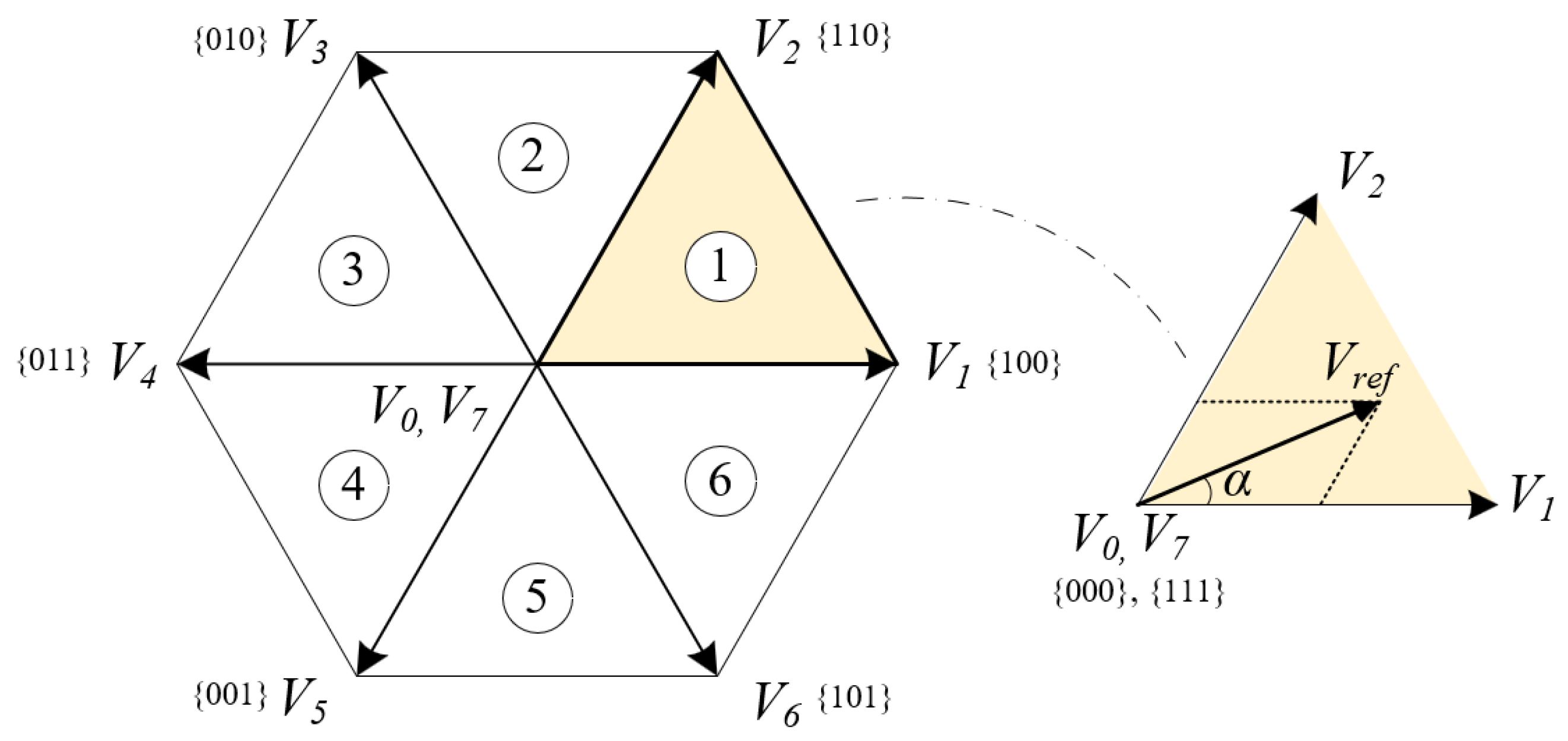
Since the three-phase SSI utilizes the B6 bridge of the standard VSI, it uses the same switching vectors ( V o V 7 ), shown in Figure 4. The inductor, L , and the diodes of Figure 3 are used to boost the supply voltage to the desired DC-link voltage at the capacitor, C d c . It is important to note that the three-phase SSI uses the switching vectors V o V 6 to charge the input inductor, while the remaining zero vector V 7 is used to discharge the inductive energy to the DC-link capacitor. The equivalent circuits of both inductive charging and discharging modes are shown in Figure 5.
(1)
Inductive Charging Mode: The charging mode can be obtained by switching ON at least one of the lower switches in the B6 bridge. In this case, the voltage at the output of the DC-side is zero (i.e., v i n v = 0 ) due to the short circuit, as shown in Figure 5a. As a result, the inductor L is charged during an interval of T c h .
(2)
Inductive Discharging Mode: The discharging mode occurs when all of the upper switches in the B6 bridge are turned ON (i.e., V7{111}). In this case, the inductor L will release its energy in the capacitor C via the antiparallel diodes of the upper switches during an interval of d d i s , where T d i s = T 7 = T s T c h , T s is the sampling time. Hence, the voltage at the DC side equals the capacitor voltage (i.e.,   v i n v = v d c ), as shown in Figure 5b.

2.3. DC Boosting Factor

The DC-boosting factor, β , which represents the ratio between the DC-link voltage, v d c (that is, the capacitor voltage), to the supply voltage, β , can be expressed as follows [16]:
β = 1 ( 1 D a v )
where D a v is the average value of the charging duty cycle ( d c h = T c h / T s ), it can be determined from D a v = 1 / T s 0 T s T c h d t .

2.4. Modulation

Several modulation schemes have been presented with the idea of level shifting to obtain the boosting and inversion processes for three-phase SSIs [16,17,18,19]. The level shifting leads to wider boosting capabilities [19]. The commonly used schemes for SSI are reviewed and compared in this section. The schemes are level-shifted sinusoidal PWM (SM), third-harmonic injection PWM (THM), symmetrical PWM (SYM), and modified space-vector PWM (MSVM), which are fully discussed in [16,25].
(1) Mathematical Relations: Considering the linear modulation operating mode, a general representation of the modulating signals, u k * , for all of the schemes using the carrier-based PWM modulators is governed by
u k * = u k + u z s s
where u z s s is the zero-sequence signal that gives us the degree of freedom to obtain the different modulation schemes; k   ϵ   { a , b , c } and u k are the basic sinusoidal three-phase modulating signals, and they can be derived from
u k = [ u a u b u c ] = M [ sin ( ϑ ) sin ( ϑ 2 π / 3 ) sin ( ϑ + 2 π / 3 ) ]
where ϑ = ω t is the fundamental angular frequency, and M is the modulation index, which can be determined from
M = μ V ^ o / V d c 0 < M < 1
where V ^ o is the maximum value of the fundamental component of the output-phase voltage, V d c is the average DC-link voltage (capacitor voltage), and μ is a modulation coefficient, which equals 2 for SM and 3 for THM, SYM, and MSVM schemes.
The duty cycles of the reference modulating signal, d k * , which are compared with the up–down carrier wave to obtain the gating pulses of the SSI, can be determined from
d k * = 1 / 2 ( 1 + u k * ) & 0 d k * 1 .
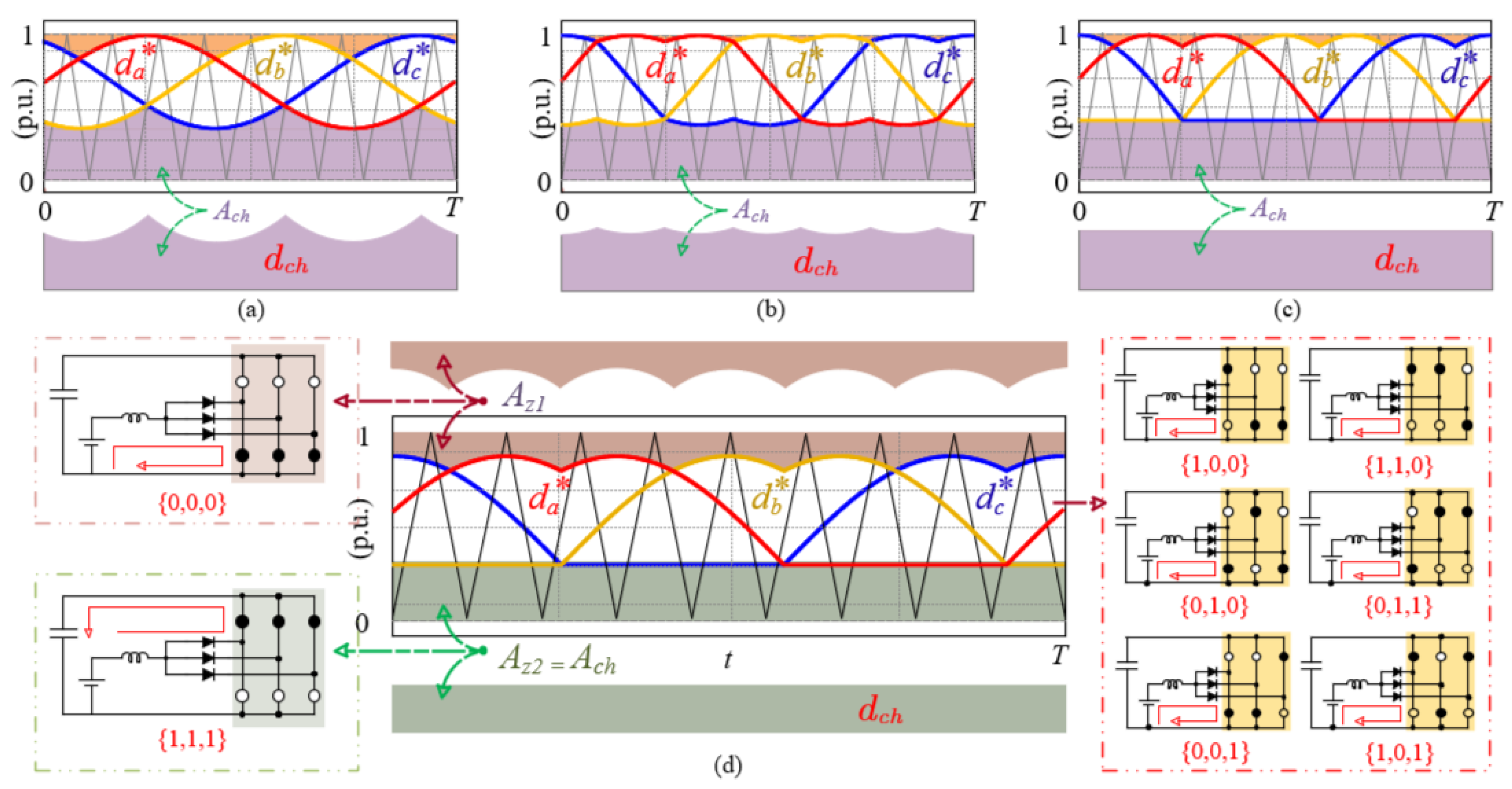
Figure 6 shows the duty cycles d k * of the selected modulation schemes. It can be observed that the charging duty cycle, d c h , is time-variant in the SM and SYM schemes, while it is fixed during the switching period in the MSVM and RSVM schemes. As a result, ripples with low-order harmonics will appear in the DC-link voltage and inductor current when SM and SYM are employed. So, from the point of view of the input current and DC-link voltage ripples, the MSVM and RSVM schemes are the best choices for SSIs.

2.5. Design Procedure

The inductor current and capacitor voltage ripples ( Δ I L , Δ V d c ) are crucial factors in the design procedure. When using MSVM and RSVM schemes, there is only a high-switching ripple based on the switching frequency, and the value of L and C are determined from [19]
L = d c h E f s w Δ I L & C = ( 1 d c h ) I L f s w Δ V d c
where f s w is the switching frequency.
It is worth noting that the value of the required passive elements L and C are increased in the case of SM and SYM schemes to mitigate the effect of low-order harmonics and obtain the same current ripples.
After reviewing the three-phase SSI, in the next sections, this paper extends the concept of the basic three-phase SSI to the five-phase case as an example of the n -phase SSI topologies.

3. Proposed Five-Phase Split-Source Inverters

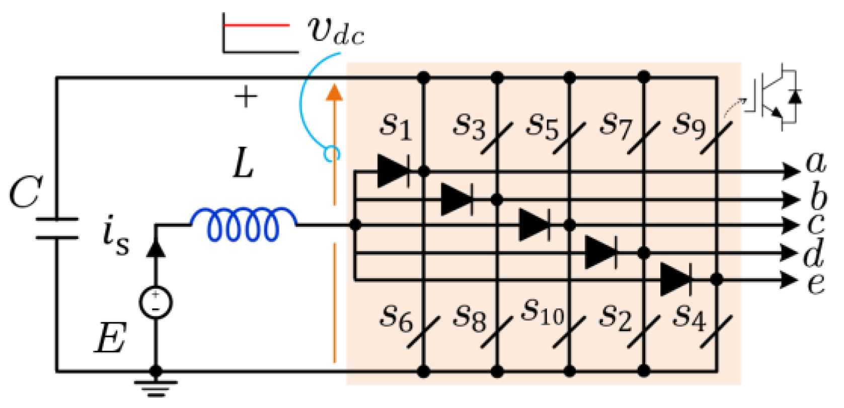
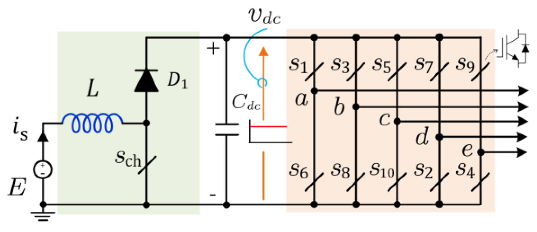
The five-phase SSI topology is shown in Figure 1. In this case, five forward diodes are used to combine the DC-boosting inductance into the multiphase inverter bridge, as shown in Figure 7. The multiphase SSI topology is used here to supply a star-connected balanced inductive load, as shown in Figure 7. The circuit is supplied by a DC-supply voltage e , which is supposed to be almost constant ( e     E ).
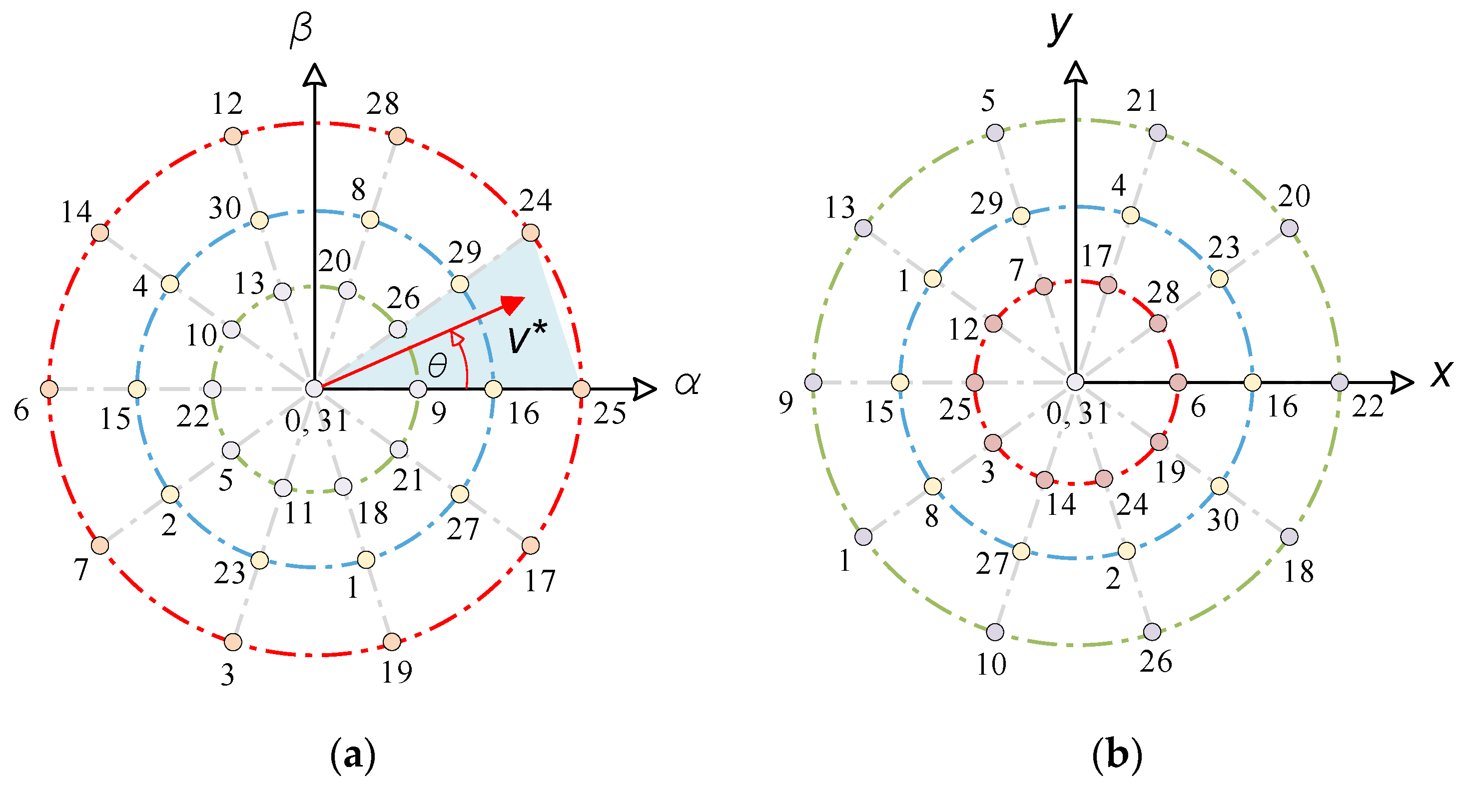
As known, there are 32 ( 2 n , n = 5 ) switching action combinations ( V o V 31 ) for the 5-phase VSI, from which two are the zero vectors ( V o and V 31 ) and the remaining are active, as shown in Figure 8. In the presented SSI topology, the switching vectors V o V 30 are used for inductive charging, while the remaining zero vector V 31 is used to release inductive energy. The equivalent circuits of inductive charging and discharging modes are shown in Figure 9a,b.
Among the best-known and reviewed PWM schemes of the 3-phase SSI is the MSVM scheme, which is developed here to control the operation of the 5-phase SSI. The modulating signals for the case of five-phase SSI can be mathematically represented as
v j = v j * + v z s s
where v j is the duty cycles of the modulating signals, and j = a ,   b ,   , e and v j * are the sinusoidal reference signals, which are shifted by 2 π n / 5 as given in (4)
v j * = k 2 M cos ( ω t 2 π n 5 ) ,   n { 0 4 }
where k 2 is a constant equal to 1 / ( 2 sin ( 2 π / 5 ) ) and ω is the line frequency in rad/s, while v z s s in (7) denotes the zero-sequence signal (ZSS) that is selected to obtain different SVM schemes, such as sinusoidal modulation (SM), fifth harmonic injection modulation (FHM), symmetrical SVM (SYM), and MSVM. The ZSS, in each case, is governed by
v z s s = { D a v   SM D a v k 2 M cos ω t   FHM D a v 1 2 k 2 ( v max + v min )   SYM D a v k 2 v min   MSVM
where v m a x and v m i n are the maximum and minimum envelop of all the sinusoidal reference signals of (9), respectively, while M is the modulation index. It is worth noting that the modulation index of any modulation technique should be limited by one.
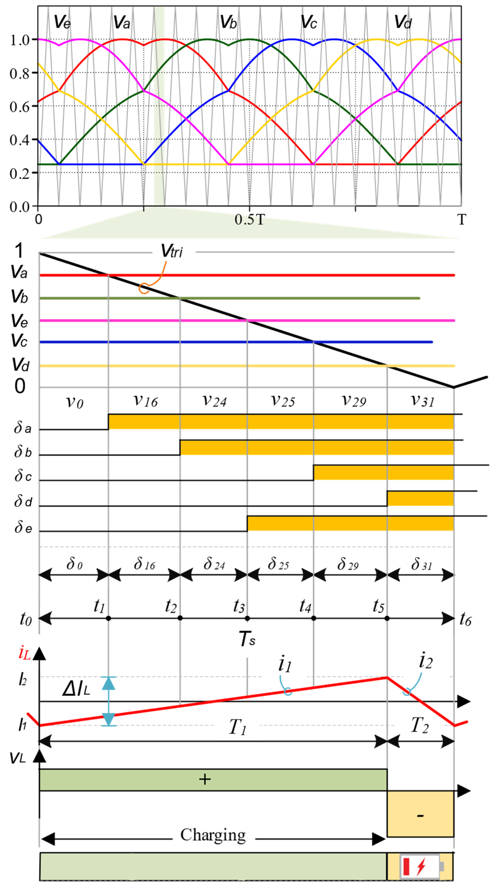
This paper focuses on the MSVM scheme, which leads to a constant DC-side current ripple. For the sake of illustration, Figure 10 shows the duty cycles of the modulating signals of the MSVM scheme of five-phase SSI, which is governed by (7)–(9) for M = 0.75. As observed in the first sector of Figure 10, v a > v b > v e > v c > v d . Therefore, the minimum voltage is v d . Thus, the five-phase duty cycles are given by
{ v a = k 2 ( v a * v d * ) + 1 M v b = k 2 ( v b * v d * ) + 1 M v c = k 2 ( v c * v d * ) + 1 M v d = 1 M v e = k 2 ( v e * v d * ) + 1 M
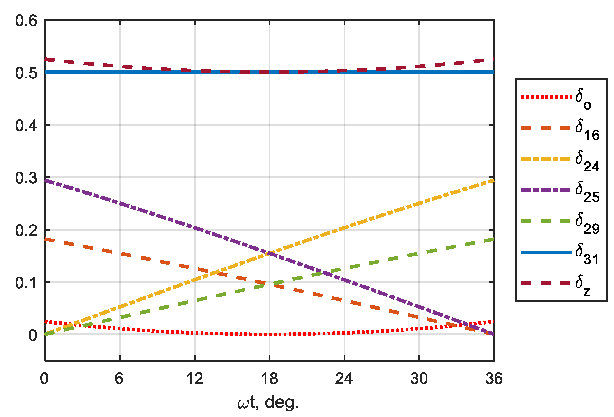
Figure 10 also shows the generation mechanism of the switching pattern in sector 1 of the five-phase SSI. Due to the symmetry, only the first half of the switching period is explained. The duty cycles of the resulting active ( δ 16 ,   δ 24 ,   δ 25 , and   δ 29 ) and zero vectors, δ z ( δ 0 and δ 31 ) in this switching pattern can be determined based on the volt-second balance concept by (11). Figure 11 shows the variations of these duty cycles for sector 1.
{ δ 0 = M ( 1 sin ( ω t + 2 π / 5 ) ) δ 16 = k 2 L M sin ( π / 5 ω t ) δ 24 = M sin ( ω t ) δ 25 = M sin ( π / 5 ω t ) δ 29 = k 2 L M sin ( ω t ) δ 31 = 1 M δ z = δ 0 + δ 31
It is worth seeing from (11) and Figure 10 that the duty cycle of the discharging mode, δ 31 , is constant during the sector. This will also lead to obtain a constant duty cycle of the charging, D , which is equal to the sum of all remaining duty cycles in a switching period and can be determined by
D = δ 0 + δ 16 + δ 24 + δ 25 + δ 29 = 1 δ 31 .
Hence,
D a v = D = M .
From (13), the DC-boosting and AC inverter gain are
β = 1 1 M & G = M 2 sin ( 2 π / 5 ) ( 1 M )
Figure 12 shows a graphical correlation between the modulation index and the DC-boosting factor for the same voltage gains. It can be observed that the five-phase SSI will operate at a wide range of modulation indices and has a directly proportional relationship between the gain and modulation index, i.e., a higher modulation index leads to greater gains. Having a lower THD of the output is one of the significant advantages of this inverter.

4. Current Ripple Analysis of Five-Phase SSI

This section introduces an analytical analysis of the DC-input current ripple, error-voltage vector, and output harmonic distortion flux (HDF), which is related to the output current ripple of five-phase SSI based on the MSVM scheme.

4.1. DC Ripple and Design of Passive Components

The inductor currents ripple of the five-phase SSI topology can be evaluated as in the basic DC–DC boost-converter. This is owed to fixing the charging and discharging intervals ( T 1 and T 2 ) of a given modulation index, which is obtained by applying the MSVM scheme. During the inductive charging mode of Figure 9a, the inductor current is given by
i 1 = E L · t + I 1
where I 1 is the initial current in charging mode. During this mode, the inductor current rises, and the inductor voltage will be positive, as shown in Figure 10.
The inductor current during the discharging mode of Figure 9b is given by
i 2 = ( E v d c ) L · t + I 2 ,
where I 2 is the initial current in the discharging mode. For a stable operation, the inductor current must fall, and therefore the inductor voltage goes to a negative value, as shown in Figure 10.
Assuming the high-frequency switching operation, the peak-to-peak inductor current ripple, and the DC-link capacitor voltage ripples as follows:
{ Δ I L = I 2 I 1 = E L D a v f s = E L M f s , Δ V C = I d c 1 D a v C f s = I d c 1 M C f s .
It can be observed from (17) that the inductor current and the capacitor voltage ripples are inversely proportional to their respective (L/C) values and the switching frequency.

4.2. AC Current Ripple

The AC ripples can be evaluated using both the time domain and the space-vector domain [26,27]. In the time-domain analysis, the output current ripple, Δ i o , is determined from
Δ i o ( t ) = i o ( t ) i o 1 ( t )
where i o is the actual output current and i o 1 is the fundamental component of the sinusoidal output current. Figure 13 shows the graphical waveforms of these currents.
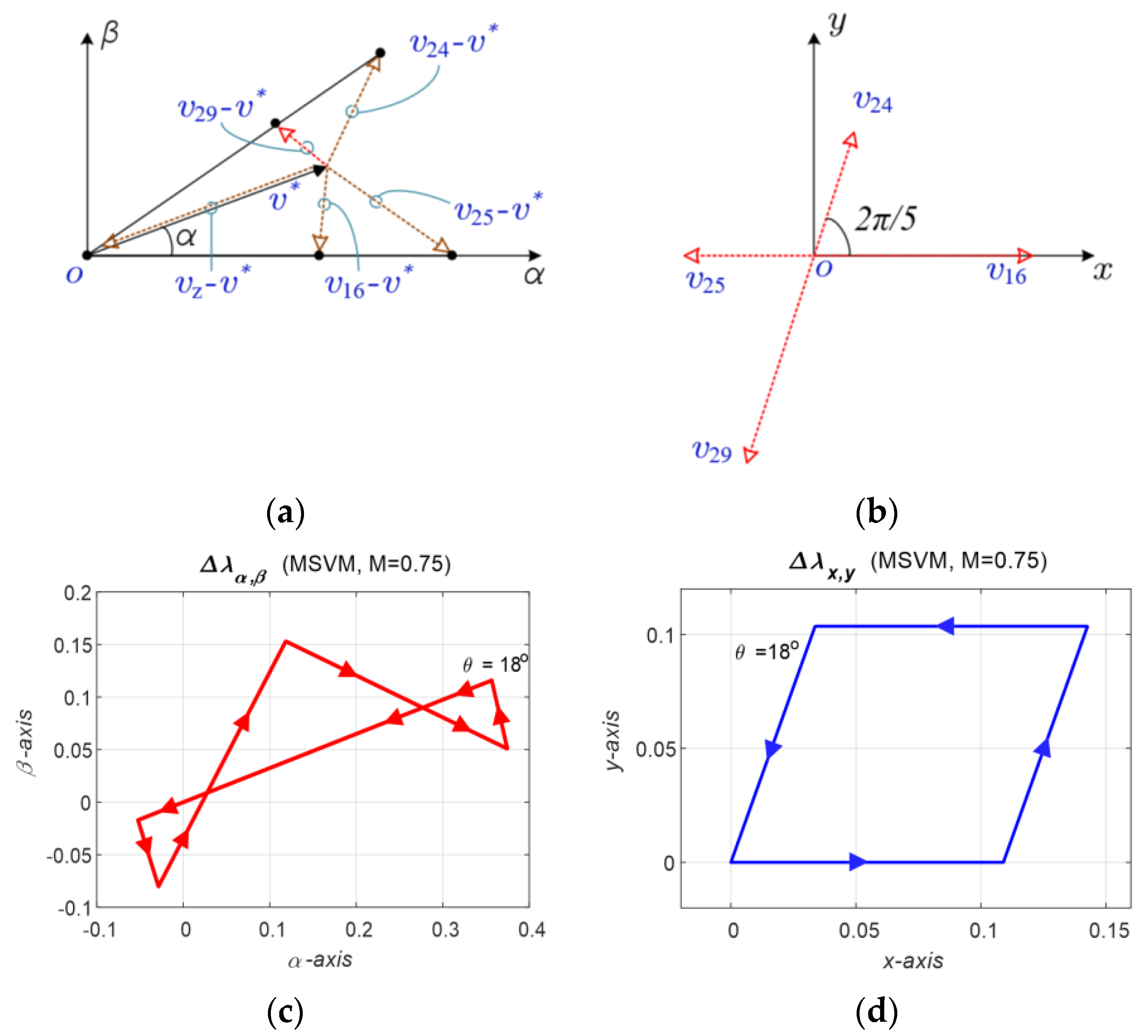
On the other hand, the analysis of the peak current ripples in this paper is based on the space-vector approach, which gives a quantitative evaluation of the current ripple [4,26,27]. Due to symmetry, only the first sector in the α β plane is examined. Figure 14a,b show how the error-voltage vectors between the reference v ¯ * and the actual space vectors, v ¯ k ( k is the vector number), are generated in both α β and x y subspaces. It should be noticed that a zero-reference space vector is assumed in the x y plane to eliminate the low-order harmonics from the output voltage waveform. Additionally, it can be observed that the error vectors depend on the index, M , and the angle θ and are defined as [4]
Δ v ¯ k ( M ,   θ ) = v ¯ k v ¯ * ( M ,   θ )
In this approach, the output current ripple, Δ i o , is evaluated from the harmonic distortion flux (HDF), Δ λ ¯ , as follows [4]
Δ i o = ( 1 / L σ ) Δ λ ¯
where L σ is the equivalent motor inductance, which can be determined in the case of induction motor drives from the stator leakage inductance, L 1 ; the rotor leakage inductance, L 2 ; and the magnetization inductance, L m , as follows [26]:
L σ = L 1 + L 2 L m L 2 + L m
The HDF, Δ λ ¯ , is defined as the error vector between the reference and actual space vectors during one switching period. It can be also called the harmonic-flux trajectory and is determined from
Δ λ j ¯ = Δ v ¯ k ( M ,   θ ) · Δ t
where Δ t is the switching period and v ¯ * ,   v ¯ are the reference and actual switching space vectors, respectively. It is worth noting that Δ λ ¯ is time-dependent, and it is a function of M and θ . In the case of five-phase inverters, the HDF should be calculated for both α β and x y subspaces.
Assuming zero initial conditions for the harmonic flux at the beginning of the switching period, Figure 14c,d show the harmonic-flux trajectory in both subspaces for M = 0.75 and θ = 18 ° . To give a fair comparison, Figure 15 shows the trajectory of the harmonic flux for both five-phase VSI and SSI. It is worth noting that the VSI is modulated by the conventional SVM, while SSI is modulated by the MSVM scheme. Based on (22), the mean-square value of the HDF in the α β and x y planes over a sampling interval ( 0 t T s ) is
Δ λ ¯ a b c d e M S 2 ( M ,   θ ) = 0 T s Δ λ ¯ j 2   d t
Hence, the per-fundamental cycle HDF, Δ λ a b c d e M S f 2 , is
Δ λ a b c d e M S f 2 ( M ) = 5 π 0 π / 5 Δ λ a b c d e M S 2   d θ .
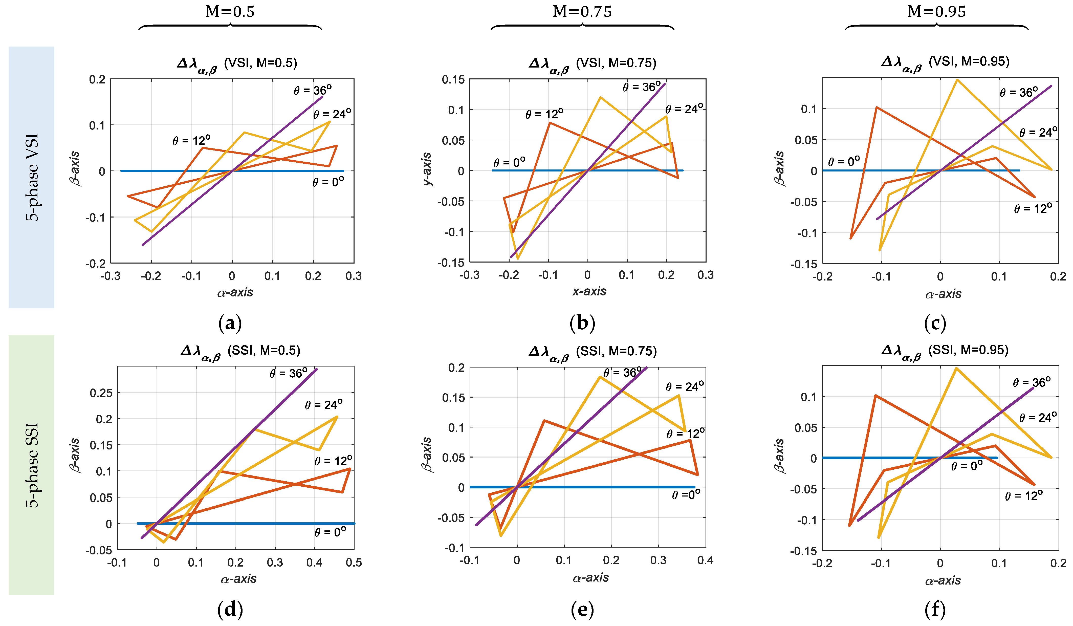
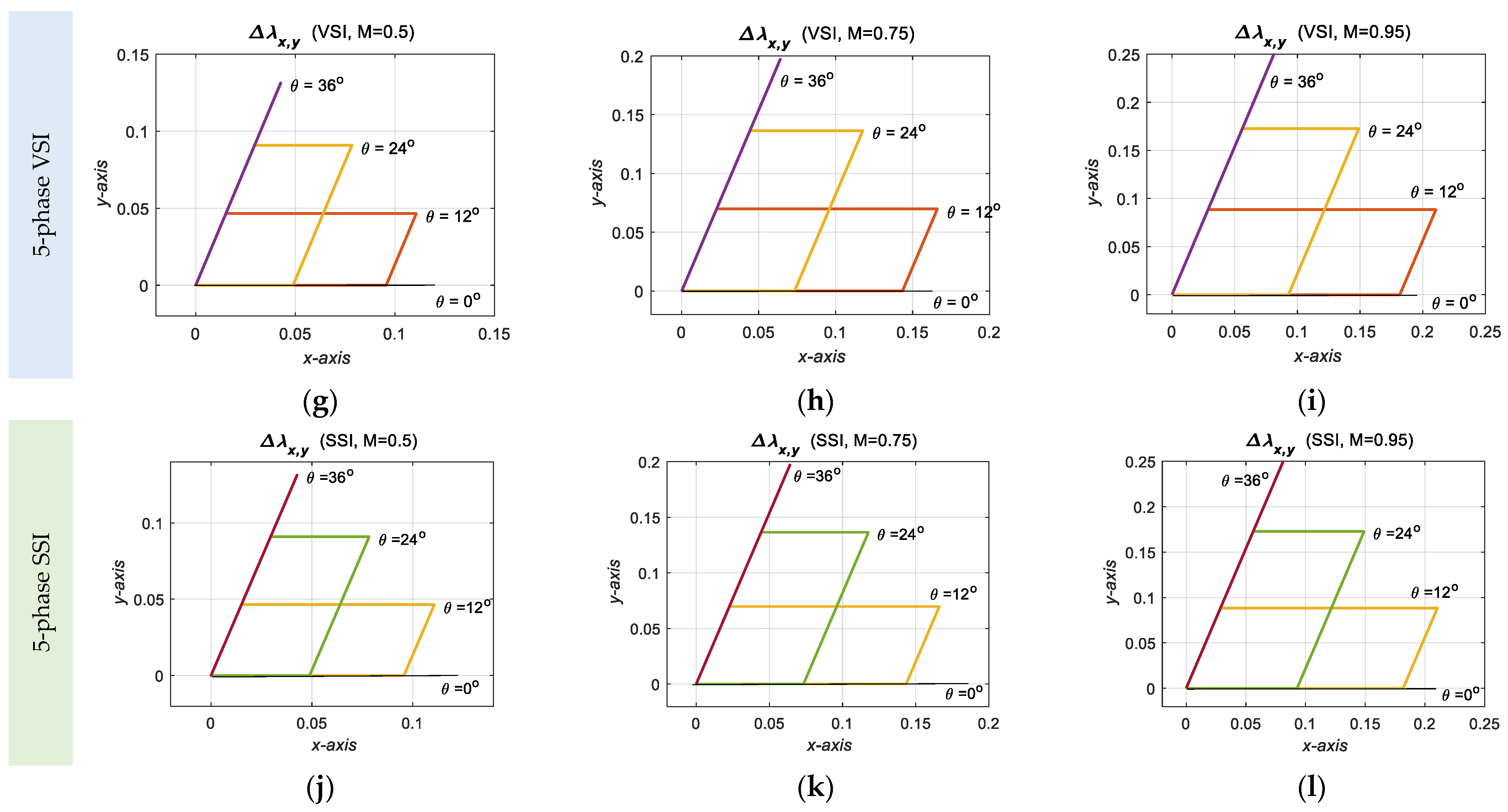
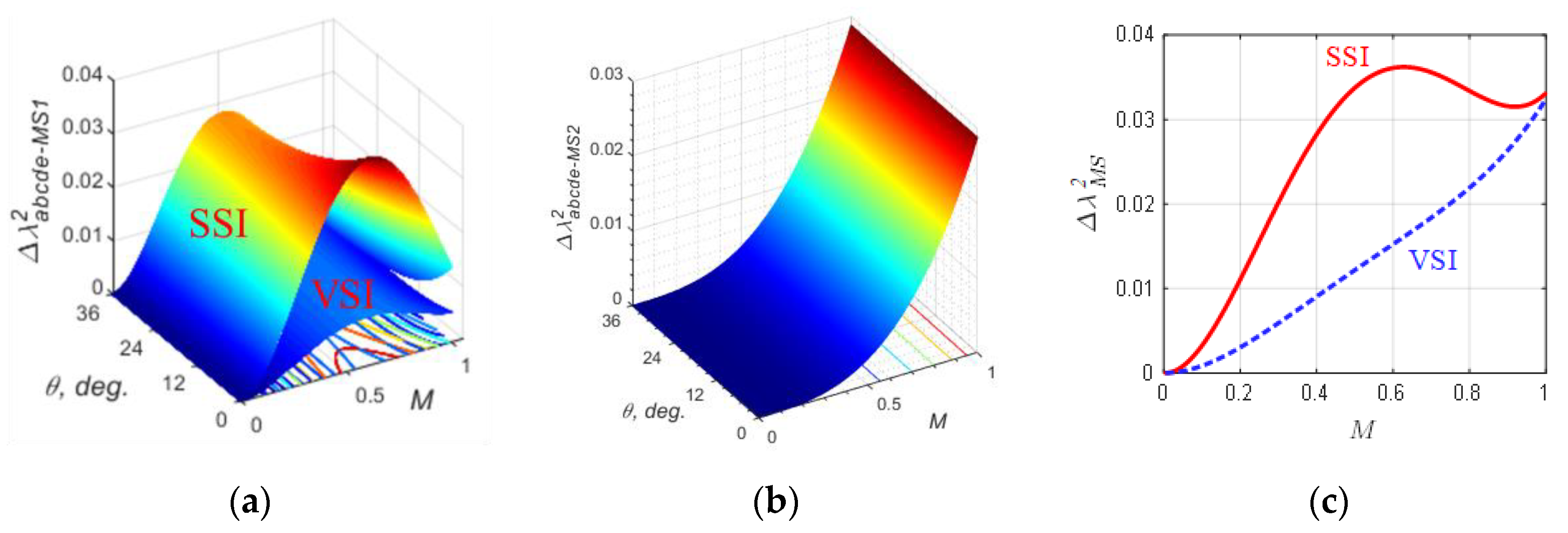
The HDF for both the five-phase VSI and SSI topologies is shown in Figure 16. The HDF is highly affected by the modulation index and modulation scheme. Based on Figure 15 and Figure 16, the following conclusions can be drawn:
Due to the symmetrical distribution of the zero vectors in the classical SVM of VSI, symmetrical harmonic flux trajectories are observed from the α β plane of Figure 15a–c, while there are some asymmetries in the MSVM for SSI because of the level shift approach, as shown in Figure 15d–f. However, the same trajectories are obtained in the x y plane, as shown in Figure 15g–l. This is owed to the zero references on this plane.
As shown in Figure 16a,b, the HDF is significantly greater for SSI than for VSI in the α β -plane, particularly for low-modulation indices. However, in the x y -plane, the HDF is the same.
Due to the elimination of the level shift effect on SSI modulating waveforms at M = 1, both VSI and SSI have approximately equal HDFs, as shown in Figure 16c.
The SSI produces higher current ripples than the traditional VSI, but since the SSI also boosts the voltage, it does not require an additional DC booster.

5. Simulation and Experimental Results

Based on the analysis, a PLECS simulation model has been developed for a five-phase SSI topology. The topology is powered by a fixed DC source of 45 V and loaded by a five-phase inductive load. Firstly, the simulation study aims to prove the concept of five-phase SSI by showing the input and output waveforms of the voltages and currents. The parameters of the simulation are listed in Table 1.
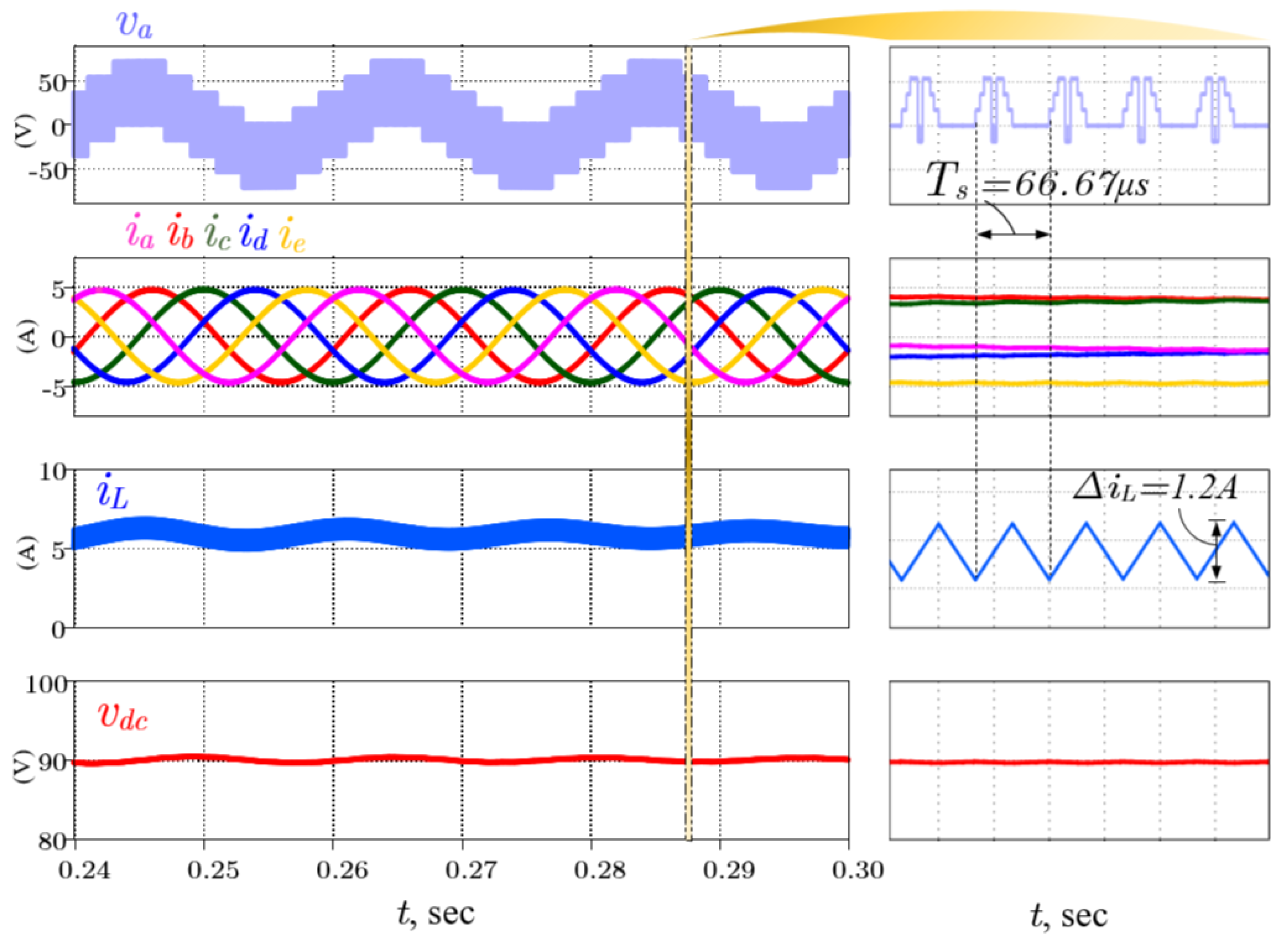
Figure 17 shows the output-phase voltage, output currents, DC-link voltage, and inductor current waveforms for the case study. Additionally, the zoom window of Figure 17 illustrates these results from a microscopic perspective to illustrate the concept and the inductor current and capacitor voltage ripples.
Based on the simulation results, it can be observed that
  • The simulated waveforms and measured values from PLECS for the five-phase SSI show good agreement with that estimated from the analysis. For example, the average DC-link voltage is 90V, and the input current ripple 1.2 A agrees with that calculated from (13) and (16), respectively, at the given condition of the case study.
  • The output-phase currents are sinusoidal waves, and the input current is completely free from the low-order harmonics. Moreover, the DC-link capacitor voltage exhibits near-constant value.
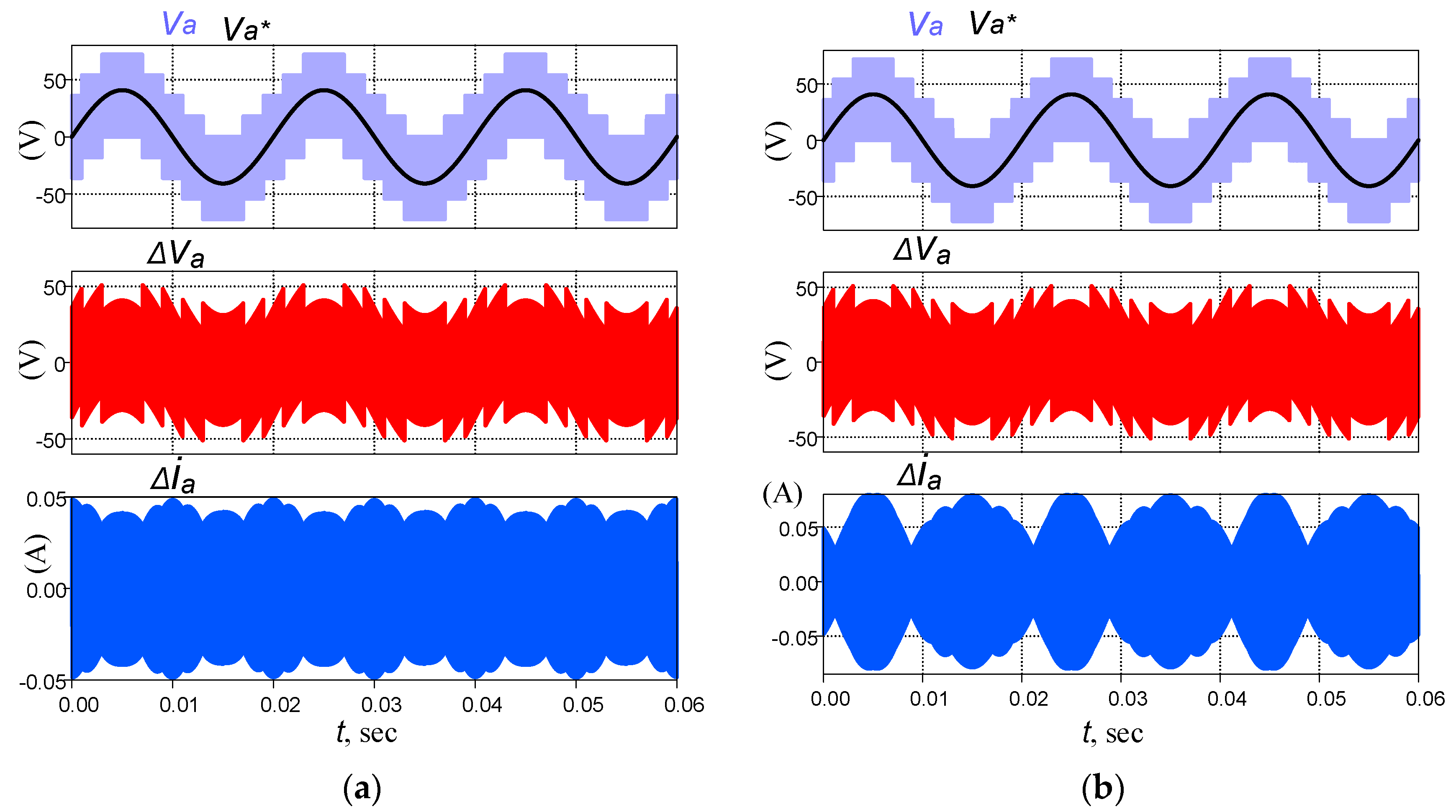
Furthermore, the proposed five-phase SSI is compared with the standard two-stage five-phase inverter shown in Figure 18, which is composed of a boost converter followed by a five-phase VSI. To obtain a fair comparison, it is important to provide the same DC-link voltage to the inverter bridge for both topologies. Therefore, the voltage supplied to VSI is determined by the expected average voltage of the DC-link capacitor in the 5-phase SSI ( V d c = β E ). In this case, the modulation index is set to 0.5 for both topologies, and the duty cycle for the boost converter stage in the conventional architecture is set to 0.5. An evaluation in terms of phase voltage and current ripples is introduced in Figure 19. As expected from the current ripple analysis of Section 4, the conventional VSI has a lower current ripple at M < 1 than the proposed SSI. However, the conventional VSI needs an extra converter stage.

6. Experimental Results

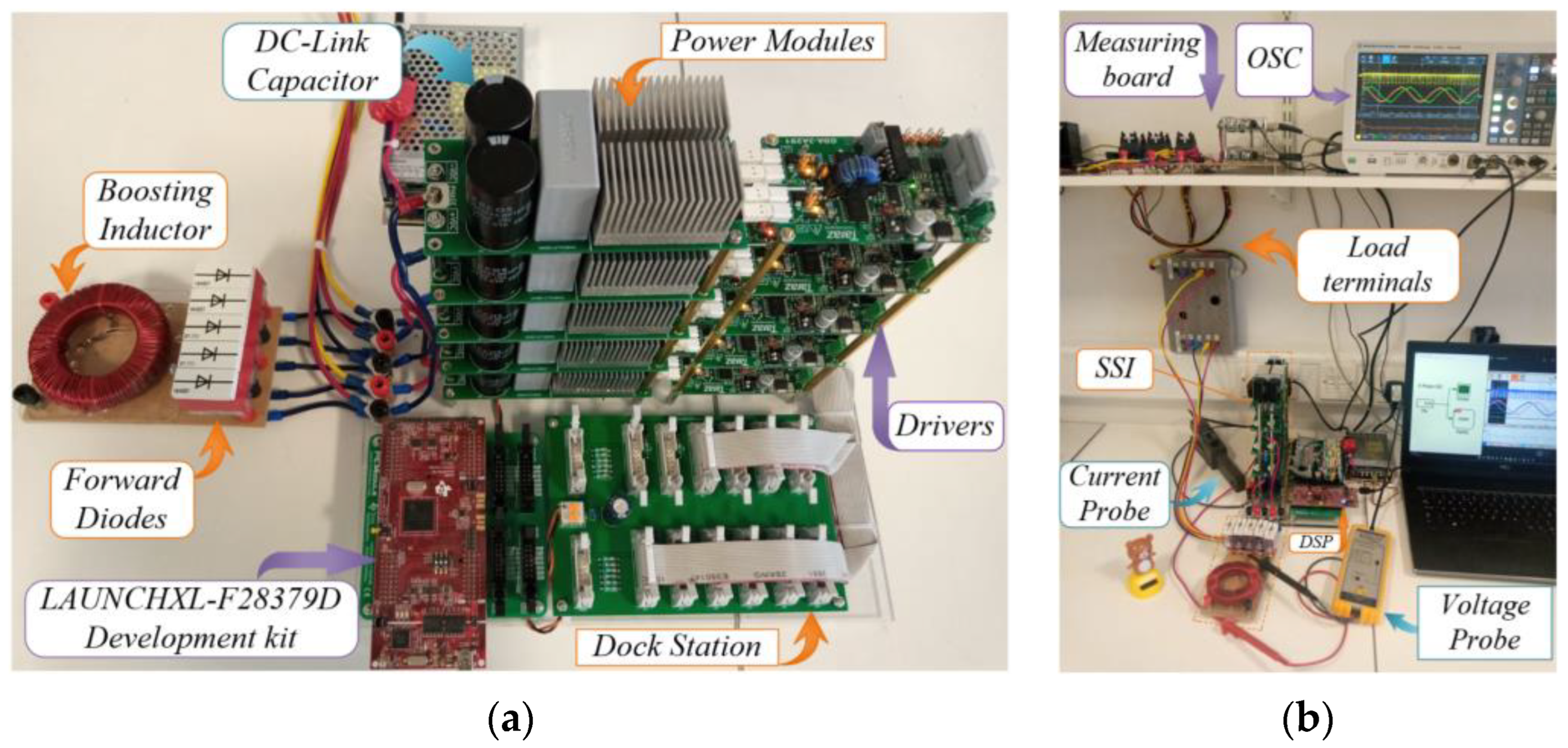
This section describes the experimental results conducted on the laboratory prototype, shown in Figure 20a, which is designed according to the presented procedure. A five-phase star-connected inductive load of 4.7 ohms and 5 mH is connected to the inverter output terminals. The whole experimental setup is shown in Figure 20b. During this study, a low-cost LaunchPad Delfino development kit (F28379D) was utilized to implement the modulation technique. To generate symmetrical triangular signals, the kit was programmed using the PLECS coder with a UP/DOWN counter at 15 kHz, while modulation signals have a modulation index of 0.5 and a frequency of 50 Hz.
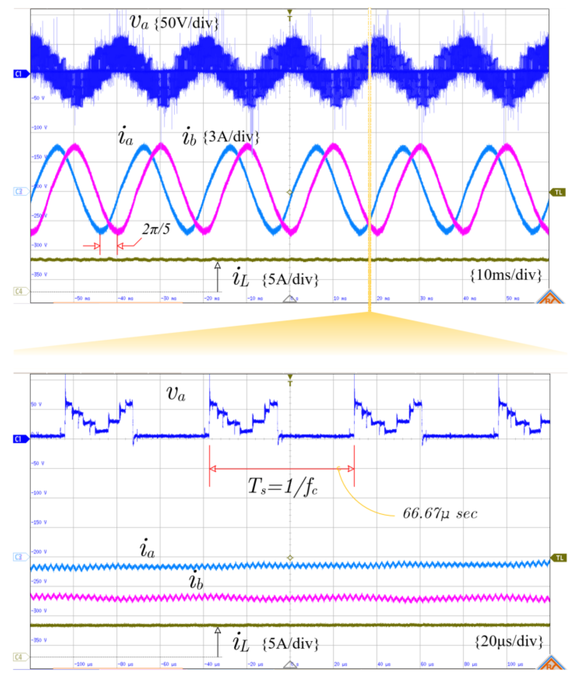
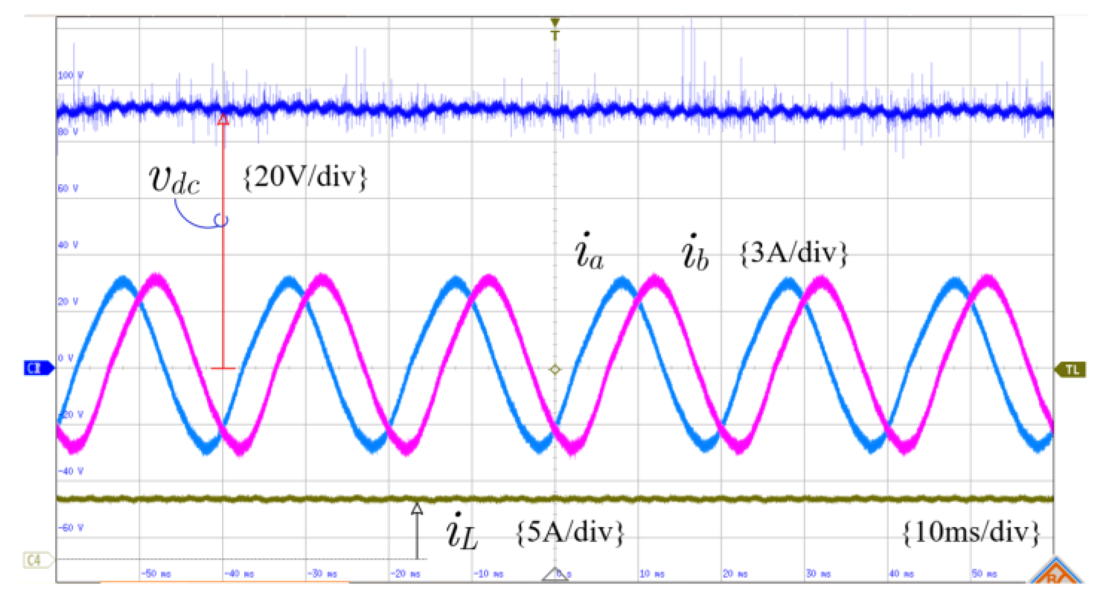
The measured voltage and current waveforms are recorded via a multi-channel digital oscilloscope from ROHDE&SCHWARZ (R&S RTM3004) [28] and shown in Figure 21, Figure 22 and Figure 23. The upper trace of Figure 21 shows the output voltage, output current, and supply current waveforms for the case study, while the lower trace shows a zoom of the measured waveforms. Moreover, Figure 22 shows the DC-link or capacitor-voltage waveform. In addition, the inductor voltage and the current stress on one of the forward diodes are shown in the upper trace of Figure 23; moreover, a zoom of the inductor voltage is shown in the down trace.
From these results, the following observation can be made:
  • Based on Figure 21, the waveforms of the output currents are near sinusoidal waveforms with low distortion and displaced by 2π/5. These results are close to the simulation results. As can be observed, the pulse width modulated output voltage is chopped according to the proposed scheme with a frequency, f c , of 15 kHz.
  • From the inductor (supply) current waveform shown in Figure 21, it is worth noting that the inductor current is free from the low-order harmonics with the proposed PWM scheme. This is owed to utilizing fixed charging and discharging duty cycles in the proposed MSVM scheme. As you can see, the inductor current is continuous, with an average value of 5.3 A.
  • The measured average voltage at the DC link from Figure 22 is 89 V. It agrees with the simulation and the mathematical analysis.
  • Moreover, it can be observed from Figure 23 that the average voltage across the inductor is zero due, which proves the volt-second balance concept.
From the analytical, simulation, and experimental studies presented in this paper, the proposed five-phase split-source inverter possesses all of the advantages of the basic three-phase topology, and it is promising for applications involving five-phase motor drives, particularly if a high-output voltage gain is required. It presents a good alternative to the counterparts of the boosting inverters.

7. Conclusions

A five-phase split-source inverter topology is presented in this paper as an example of the multiphase architecture of the basic split-source inverter. This topology shows a good alternative for the low-voltage-supplied five-phase drive system, which is based on the basic two-stage DC–DC–AC converter and Z-source inverters. The paper discusses in detail the operating principles and modulation technique of the proposed topology. Furthermore, a detailed analysis of the ripples in the input and output currents is presented along with graphical representations. In addition, the results of the theoretical study are verified and validated through a simulation study using PLECS. An experimental prototype is built to validate the theoretical analysis. Simulation and experimental results are clearly in agreement, and experimental differences can be attributed to deadtime parasitic effects.
To conclude the findings behind this work, the five-phase SSI topology has some merits over its counterparts, which are used particularly if a high-output voltage gain is required. In summary, these merits are as follows:
(a)
It has a continuous input current free of low-order harmonics;
(b)
The AC-output ripple is like that of the conventional space vector modulated five-phase VSIs; therefore, these ripples are smaller than those of Z-source inverters.
(c)
The boosting action is performed in a single stage, with fewer passive elements than Z-source inverters and without active switches as in two-stage inverters.
(d)
In addition, it uses the same standard modulation schemes as the five-phase inverter and there is no need for additional shoot-through pulses.
Moreover, it is also possible to apply the same concept of this study to the other multiphase SSI topologies such as six-phase, seven-phase, and nine-phase architectures, and the same conclusions can be drawn.

Author Contributions

Conceptualization, software, methodology, validation, and formal analysis, S.M.D.; investigation, A.A.A.; resources, M.E.F.; experimental work, M.A.E.; writing—original draft preparation, S.M.D., I.A.G.; writing—review and editing, A.A.A. and I.A.G.; visualization, supervision, M.E.F.; project administration, S.M.D.; All authors have read and agreed to the published version of the manuscript.

Funding

This research received no external funding.

Institutional Review Board Statement

Not applicable.

Informed Consent Statement

Not applicable.

Data Availability Statement

Not applicable.

Conflicts of Interest

The authors declare no conflict of interest.

References

  1. Kindl, V.; Cermak, R.; Ferkova, Z.; Skala, B. Review of Time and Space Harmonics in Multi-Phase Induction Machine. Energies 2020, 13, 496. [Google Scholar] [CrossRef] [Green Version]
  2. Laksar, J.; Cermak, R.; Hruska, K. Challenges in the Electromagnetic Design of Multiphase Machines: Winding and Equivalent Circuit Parameters. Energies 2021, 14, 7335. [Google Scholar] [CrossRef]
  3. Dabour, S.M.; Rashad, E.M.; Abdel-khalik, A.; Ahmed, S.; Massoud, A. A new fifteen-switch inverter topology for two five-phase motors drive. In Proceedings of the 2016 Eighteenth International Middle East Power Systems Conference (MEPCON), Cairo, Egypt, 27–29 December 2016; pp. 729–734. [Google Scholar] [CrossRef]
  4. Dabour, S.M.; Abdel-Khalik, A.S.; Massoud, A.M.; Ahmed, S. Analysis of Scalar PWM Approach With Optimal Common-Mode Voltage Reduction Technique for Five-Phase Inverters. IEEE J. Emerg. Sel. Top. Power Electron. 2019, 7, 1854–1871. [Google Scholar] [CrossRef] [Green Version]
  5. Elgenedy, M.A.; Elserougi, A.A.; Abdel-Khalik, A.S.; Massoud, A.M.; Ahmed, S. A Space Vector PWM Scheme for Five-Phase Current-Source Converters. IEEE Trans. Ind. Electron. 2016, 63, 562–573. [Google Scholar] [CrossRef]
  6. Dabour, S.M.; Abdel-Khalik, A.; Ahmed, S.; Massoud, A. Performance of a three-to-five matrix converter fed five-phase induction motor under open-circuit switch faults. In Proceedings of the ISCAIE, Penang, Malaysia, 30–31 May 2016; pp. 159–164. [Google Scholar]
  7. Ellabban, O.; Abu-Rub, H. Field-oriented control of a five-phase induction motor fey by a Z-source inverter. In Proceedings of the 2013 IEEE International Conference on Industrial Technology (ICIT), Cape Town, South Africa, 25–28 February 2013; pp. 1624–1629. [Google Scholar] [CrossRef]
  8. Abduallah, A.A.; Iqbal, A.; Meraj, M.; Ben-Brahim, L.; Alammari, R.; Abu-Rub, H. Discontinuous space vector pulse width modulation techniques for a five-phase quasi Z-source inverter. In Proceedings of the IECON 2015-41st Annual Conference of the IEEE Industrial Electronics Society, Yokohama, Japan, 9–12 November 2015; pp. 004205–004210. [Google Scholar] [CrossRef]
  9. Ellabban, O.; Abu-Rub, H. Z-Source Inverter: Topology Improvements Review. IEEE Ind. Electron. Mag. 2016, 10, 6–24. [Google Scholar] [CrossRef]
  10. Kavya Santhoshi, B.; Mohana Sundaram, K.; Padmanaban, S.; Holm-Nielsen, J.B. Critical Review of PV Grid-Tied Inverters. Energies 2019, 12, 1921. [Google Scholar] [CrossRef] [Green Version]
  11. Abdelhakim, A.; Blaabjerg, F.; Mattavelli, P. Modulation Schemes of the Three-Phase Impedance Source Inverters—Part I: Classification and Review. IEEE Trans. Ind. Electron. 2018, 65, 6309–6320. [Google Scholar] [CrossRef]
  12. Yuan, J.; Yang, Y.; Blaabjerg, F. A Switched Quasi-Z-Source Inverter with Continuous Input Currents. Energies 2020, 13, 1390. [Google Scholar] [CrossRef] [Green Version]
  13. Yi, F.; Cai, W. A Quasi-Z-Source Integrated Multiport Power Converter as Switched Reluctance Motor Drives for Capacitance Reduction and Wide-Speed-Range Operation. IEEE Trans. Power Electron. 2016, 31, 7661–7676. [Google Scholar] [CrossRef]
  14. Dabour, S.M.; Abdel-Khalik, A.S.; Ahmed, S.; Massoud, A.M. A Family of Discontinuous PWM Strategies for Quasi Z-Source Nine-Switch Inverters. IEEE Access 2021, 9, 169161–169176. [Google Scholar] [CrossRef]
  15. Ribeiro, H.; Pinto, A.; Borges, B. Single-stage DC-AC converter for photovoltaic systems. In Proceedings of the IEEE Energy Conversion Congress and Exposition, Atlanta, GA, USA, 12–16 September 2010; pp. 604–610. [Google Scholar]
  16. Abdelhakim, A.; Mattavelli, P.; Spiazzi, G. Three-Phase Split-Source Inverter (SSI): Analysis and Modulation. IEEE Trans. Power Electron. 2016, 31, 7451–7461. [Google Scholar] [CrossRef]
  17. Akbar, F.; Cha, H.; Ahmed, H.F.; Khan, A.A. A Family of Single-Stage High-Gain Dual-Buck Split-Source Inverters. IEEE J. Emerg. Sel. Top. Power Electron. 2020, 8, 1701–1713. [Google Scholar] [CrossRef]
  18. Chen, M.; Yin, C.; Loh, P.C. Magnetically Coupled High-Voltage-Boost Split Y-Source Inverter Without Leakage-Induced Voltage Spikes. IEEE Trans. Ind. Electron. 2020, 67, 5444–5455. [Google Scholar] [CrossRef]
  19. Dabour, S.M.; Alotaibi, M.A.; Abd-Elaziz, A.A.; Alshahat, M.A.; Abdallah, M.; Eltamaly, A.M.; Abdel-Khalik, A.S.; Massoud, A.M.; Ahmed, S. Modeling and Control of Single-Stage Quadratic-Boost Split Source Inverters. IEEE Access 2022, 10, 24162–24180. [Google Scholar] [CrossRef]
  20. AbdulSalam, M.; Dabour, S.M.; Rashad, E.M. Cascaded Multilevel Split-Source Inverters: Analysis and Modulation. In Proceedings of the 2019 21st International Middle East Power Systems Conference (MEPCON), Cairo, Egypt, 17–19 December 2019; pp. 1204–1209. [Google Scholar] [CrossRef]
  21. Montazeri, S.H.; Milimonfared, J.; Zolghadri, M. A New Modeling and Control Scheme for Cascaded Split-Source Converter Cells. IEEE Trans. Ind. Electron. 2022, 69, 7618–7628. [Google Scholar] [CrossRef]
  22. Montazeri, S.H.; Milimonfared, J.; Zolghadri, M.R. Multidimensional Pulsewidth Modulation for Cascaded Split-Source Inverter. IEEE Trans. Ind. Electron. 2023, 70, 137–146. [Google Scholar] [CrossRef]
  23. Dabour, S.M.; Abdel-Khalik, A.S.; Ahmed, S.; Massoud, A. An Optimal PWM Technique for Dual-Output Nine-Switch Boost Inverters With Minimum Passive Component Count. IEEE Trans. Power Electron. 2021, 36, 1065–1079. [Google Scholar] [CrossRef]
  24. Pinjala, M.K.; Bhimasingu, R. Improving the DC-Link Utilization of Nine-Switch Boost Inverter Suitable for Six-Phase Induction Motor. IEEE Trans. Transp. Electrif. 2020, 6, 1177–1187. [Google Scholar] [CrossRef]
  25. Abdelhakim, A.; Mattavelli, P.; Boscaino, V.; Lullo, G. Decoupled Control Scheme of Grid-Connected Split-Source Inverters. IEEE Trans. Ind. Electron. 2017, 64, 6202–6211. [Google Scholar] [CrossRef]
  26. Dabour, S.M.; Aboushady, A.A.; Elgenedy, M.A.; Gowaid, I.A.; Farrag, M.E. Current Ripple Evaluation of Space Vector Modulated Five-Phase Split-Source Inverters. In Proceedings of the 2022 57th International Universities Power Engineering Conference (UPEC), Istanbul, Turky, 30 August–2 September; pp. 1–6. [CrossRef]
  27. Dujic, D.; Jones, M.; Levi, E. Analysis of Output Current Ripple RMS in Multiphase Drives Using Space Vector Approach. IEEE Trans. Power Electron. 2009, 24, 1926–1938. [Google Scholar] [CrossRef]
  28. Rohde & Schwarz R&S®RTM3000 Oscilloscope. Available online: https://www.rohde-schwarz.com/uk/products/test-andmeasurement/oscilloscopes/rs-rtm3000-oscilloscope_63493-427459.html (accessed on 10 October 2021).
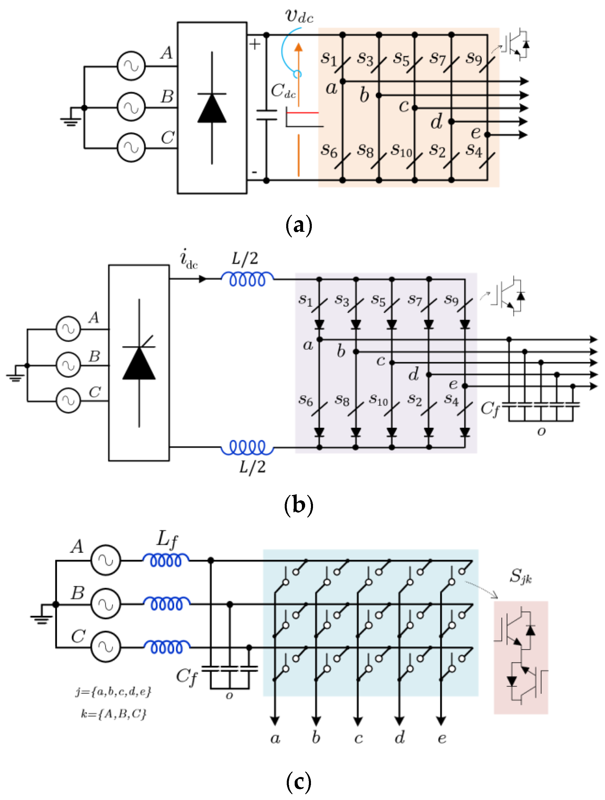
Figure 1. Basic power converters for five-phase drives. (a) Five-phase voltage-source inverter (VSI) [4]. (b) Five-phase current-source inverter (CSI) [5]. (c) Three-phase to five-phase matrix converter (MC) [6].
Energies 15 08411 g001
Figure 2. Z-source topologies for five-phase drives. (a) Basic five-phase Z-source inverter [7]. (b) Five-phase quasi-Z-source inverter [8].
Energies 15 08411 g002
Figure 3. Basic SSI topology, (a) single-phase SSI [15], and (b) three-phase SSI [16].
Energies 15 08411 g003
Figure 4. Switching state representation of three-phase SSI based on space-vector approach.
Energies 15 08411 g004
Figure 5. Mode of operation of three-phase SSI [14]. (a) Basic SSI topology (for states V0V6). (b) Inductive discharging (for state V7).
Energies 15 08411 g005
Figure 6. Modulation of three-phase split-source inverter based on level-shifted approach. (a) SM, (b) SYM, (c) MSVM, (d) and RSVM scheme. The superscript * denotes the reference waveform.
Energies 15 08411 g006
Figure 7. Five-phase SSI topology.
Energies 15 08411 g007
Figure 8. Space-vector model five-phase SSI. (a) α β subspace. (b) x y subspace.
Energies 15 08411 g008
Figure 9. Operating modes of five-phase SSI. (a) Inductive charging (for states 0–30). (b) Inductive discharging (for state 31).
Energies 15 08411 g009
Figure 10. Duty cycles of the modulating signals of 5-phase SSI for M = 0.75 for one complete period and inductor current and voltage waveforms for sector 1.
Energies 15 08411 g010
Figure 11. The variation of duty cycles during sector −1 for M = 0.5.
Energies 15 08411 g011
Figure 12. Modulation index and boosting factor versus the AC-gain of the MSVM scheme for the five-phase SSI.
Energies 15 08411 g012
Figure 13. Evaluation of AC output current ripple using the time-domain analysis.
Energies 15 08411 g013
Figure 14. Generation of error voltage vector and harmonic-flux trajectory during the half of the switching cycle of five-phase SSI using MSVM scheme [26]. (a) Generated error-voltage vectors in α β subspace. (b) Generated error-voltage vectors in x y subspace. (c) Harmonic-flux trajectory for M = 0.75, θ = 18 ° in α β plane. (d) Harmonic-flux trajectory for M = 0.75, θ = 18 °   x y plane.
Energies 15 08411 g014
Figure 15. Error-voltage vector and harmonic-flux trajectory during the half of the switching cycle for VSI and SSI [26].
Energies 15 08411 g015aEnergies 15 08411 g015b
Figure 16. Harmonic distortion flux for both five-phase VSI and SSI [26]. (a) HDF in α β plane for both VSI and SSI. (b) HDF in x y plane for both VSI and SSI. (c) Total HDF for both VSI and SSI.
Energies 15 08411 g016
Figure 17. Simulated voltages and current waveforms of the five-phase SSI under the case study using PLECS.
Energies 15 08411 g017
Figure 18. Evaluation of AC output current ripple using the time-domain analysis.
Energies 15 08411 g018
Figure 19. The simulation waveform of output-phase voltage, error voltage, and the corresponding current ripples for both VSI and SSI topologies. (a) Boost-converter followed by five-phase VSI. (b) Proposed five-phase SSI.
Energies 15 08411 g019
Figure 20. Photographs of the five-phase SSI prototype and experimental setup. (a) SSI. (b) Setup.
Energies 15 08411 g020
Figure 21. Experimental waveforms of output-phase voltage, two adjacent phase currents, and the supply or inductor current for the proposed five-phase SSI with the modified space-vector modulation scheme.
Energies 15 08411 g021
Figure 22. DC-link voltage and input/output current waveforms.
Energies 15 08411 g022
Figure 23. Five-phase SSI prototype.
Energies 15 08411 g023
Table 1. Simulation parameters for five-phase SSI.
ParametersValuesParametersValues
Input voltage45 VInput inductance1.28 mH
DC-link capacitor480 μFRL-load4.7 Ω, 5 mH
Modulation index0.5Switching frequency15 kHz
Publisher’s Note: MDPI stays neutral with regard to jurisdictional claims in published maps and institutional affiliations.