Review

Review of the Chosen Methods of Producing Front Contacts to Transparent Conductive Oxides Layers in Photovoltaic Structures

by
Małgorzata Musztyfaga-Staszuk
1,*,
Artur Czupryński
1 and
Rossen Radev
2
1
Welding Department, Silesian University of Technology, Konarskiego 18A, 44-100 Gliwice, Poland
2
Department of Materials Science and Technology, Faculty of Mechanical and Manufacturing Engineering, University of Ruse, 8 Studentska St., 7017 Ruse, Bulgaria
*
Author to whom correspondence should be addressed.
Energies 2022, 15(23), 9026; https://doi.org/10.3390/en15239026
Submission received: 24 October 2022 / Revised: 16 November 2022 / Accepted: 25 November 2022 / Published: 29 November 2022
(This article belongs to the Special Issue Advances in Materials for Electrochemical Energy Applications 2024)

Abstract

:
It is well known that PV thin films can be deposited by an extensive range of more or less expensive and complicated techniques (such as sputtering, chemical vapor deposition (CVD), physical vapor deposition (PVD), pulsed laser deposition, atomic layer deposition (ALD)). The present paper focuses on TCO layers applied by chosen techniques, including mainly the ALD and CVD methods. Thin layers of transparent conductive oxides constitute a well-known group of materials with unique properties. Oxides such as ZnO, SnO2, and In2O3 are the most significant materials of this type; some of them are discussed in the paper. From the application point of view in the photovoltaic industry, the goal is to apply a method that will provide the highest value of electric charge conductivity while maintaining the minimum value of absorption in the layer and a reduced value of the reflection coefficient. The implementation of significant achievements in the coming decade is for developing guidelines for metallization processes and TCO layers deposited by the ALD method. The work contains chosen engineering processes, including the fabrication of transparent conductive oxides (TCO) thin films applied to silicon substrates by ALD and CVD for application as emitter conductive coatings in photovoltaic structures and the fabrication front metallization of solar cell using different techniques, including among others laser techniques. Moreover, the work also contains predictions about solar cells, which will be among the most prevalent solar cells in mass production using thin- and thick-film technology.

1. Introduction

Progress in producing photovoltaic cells with ever-higher efficiency has been made in recent years, mainly thanks to modern techniques and materials, enabling the intensive development of individual stages of their production [1]. Innovative, which cannot be seen at first glance, able to effectively convert sunlight into electricity, turn out to be transparent conductive layers—transparent to light and at the same time perfectly conductive to electricity [2]; the photovoltaic sector (PV) has enormous development potential, and can be considered a new and extremely promising branch of the global industry. The most significant factor in the growth of the photovoltaic market is the constant reduction of the cost of obtaining 1 Wp of power from the energy converter. This means that producers of PV panels/modules must achieve higher energy conversion efficiency parameters, namely increasing the conversion efficiency of the solar cell and the photovoltaic (PV) module, as well as reducing costs in the process of production [3].
The sun is an inexhaustible energy source, so the current challenge that scientists worldwide are facing is to increase the efficiency of cells—maximize the value of the quotient: cell efficiency/production cost. The development of photovoltaics is the answer to the growing demand of the energy sector for new renewable electricity solutions, primarily due to the energy transition in Poland resulting from the global pandemic and the war with Ukraine. However, this development will not be possible without systemic solutions, i.e., financial support from the state and local authorities and research work in this area (Table 1). Renewable sources are slowly beginning to play an increasingly important role in this development, but also gas sources and the PV photovoltaic sector has enormous development potential. The article’s authors focused on one application criterion in technology development in the chosen area of the photovoltaic industry, item 3 of Table 1.
Production technologies and the application of surface layers have a stable position and are regarded as basic knowledge in the field of material engineering. Many research centers worldwide working on surface engineering are applying all possible means to describe the phenomena taking place on the surface of solids. Such a situation instigates scientists to undertake challenging research to determine the effect of conditions deposition of TCOs layers by various techniques and minimize electrical and optical losses occurring in functional layers of the entire ready electronic structure.
In light of the analysis of the literature review, the authors set out two new directions worthy of attention for further research. As new, experimentally obtained results in the temperature field of applying transparent conductive oxides on the contact metallization, one of the current research directions is the deposition of emitter conductive coatings, so layers of Transparent Conductive Oxides (TCOs) in photovoltaic structures by atomic layer deposition (ALD) [5].
On the other hand, the innovative nature of the research will concern the development of process engineering, which can include the presented dependence of the influence of lasermicro-machining on the improvement of the quality of the metallic component by minimizing the resistance of the connection of this front component with the substrate. Laser techniques are used in many areas of industry, including, among others, cutting, drilling, drawing, inspection and detection of quality defects in photo-elements, and shaping of material properties and structure [6]. Laser technology in producing photovoltaic cells with high efficiency in converting solar radiation into electricity is becoming an indispensable component of modern photovoltaic technology [7]. The components and functional layers of a silicon photovoltaic cell can include the layer forming the emitter of the solar cell, the passivation and anti-reflection layer, and the front and back electrodes [8,9].
According to the requirement of the EU Directive 2009/28/EC of the European Parliament and the Council, the increase in the use of renewable energy sources (RES) in the balance of final energy will be up to 20% in 2030. So the direction of the measures taken under this article is in line with the implementation of the Polish Energy Policy until 2030 [10].

2. Metal Grids

One of the current research topics in scientific units is the reduction of covering the front side of the cell by electrode contact paths, minimizing the so-called cover factor. In 2016, the width of the printed path of the front electrode was lower than 50 µm, while the same in-line printing was reduced to a level below 20 µm [11]. In 2031, it is expected that the width of the path will be reduced from 34 to 20 μm, and overprint in line with greater precision will be reduced from 10 to 6 μm. In 2021, the number of busbars in these solar cells was from 5 to 6, but in 2031 it will increase to more than 12 [11]. Figure 1 presents the market share of single- and double-sided solar cells. It is expected that from 2025 to 2025, the share of double-sided solar cells will prevail, although the share of single-sided solar cells will remain at about 40%.
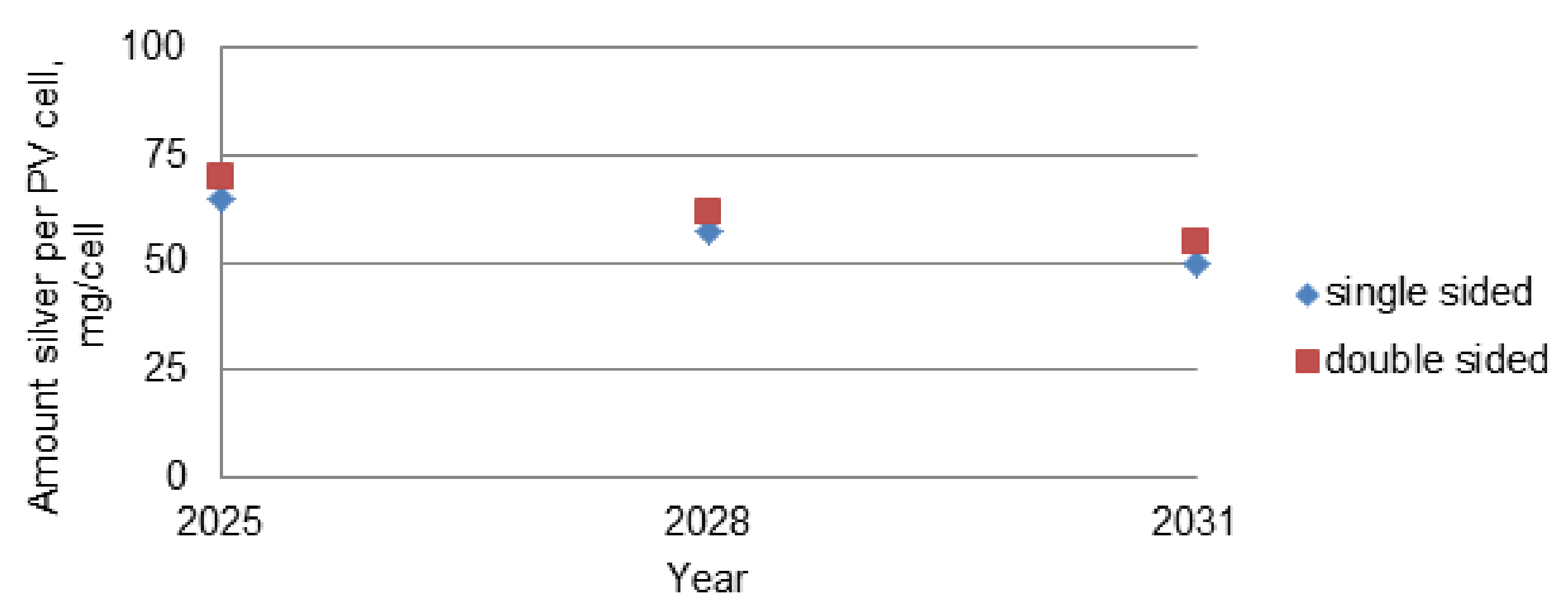
Figure 2 shows some estimations concerning reducing silver pastes/inks, the most expensive materials used in c-Si cell technologies. It is predicted during the following years to continue the reduction of silver per PV cell. In 2021 it was 80 mg for standard Passivated Emitter and Rear Contact (PERC), both single- and double-sided PV cells in the mentioned format in Figure 2. In 2031 we expected a reduction down to 50 mg per PV cell [3].
The electrode application process must meet the requirements of, among others, industrial, such as high efficiency and low cost of production. It does not include photolithography, vacuum deposition techniques, and many chemical methods, as they involve too many manufacturing steps [12]. In practice, various industrial techniques can be applied to the front electrode [13]. The most common of these is the screen printing method, which is quick and straightforward and uses pastes based on silver and aluminium; it has been used since 1975 [14]. Since then, this method has evolved rapidly and has become the dominant technique in the photovoltaic industry. Yet the coating process of silicon layer using silk-screen printing is time-consuming and challenging to automate. The height adjustment of the coated layer necessitates the application of additional screens, which translates itself into additional costs. The mechanical load applied on the wafer/insert during electrode coating can bring about numerous cracks in it and other damage. Saving on the material through the recovery of its surplus as compared to other methods is impossible in this method since only pastes can be applied here instead of, for example, powders. Taking into account material factors and fabrication conditions (having an impact on quality, in particular with the application of pastes and powders) as well as economic factors, it seems to be grounded that further experimental research involving the initial phases of the process should be carried out [15,16,17].
Today, 95% of solar cells are metaled using this method. Compared to other methods, it is anticipated that the front electrode screening technique will remain the leading technique. In recent years, the design of screen printers has been improved, making it possible to produce more than 1500 cells per hour [18]. Lack of process repeatability with smaller path widths can significantly reduce the efficiency of solar cells by the influence of factors such as paste viscosity and clogging of the mesh or leaving traces of the screen mesh. It is assumed that forming metal contacts using the stencil printing technique is one of the most cost-effective solutions for producing high-efficiency solar cells [19].
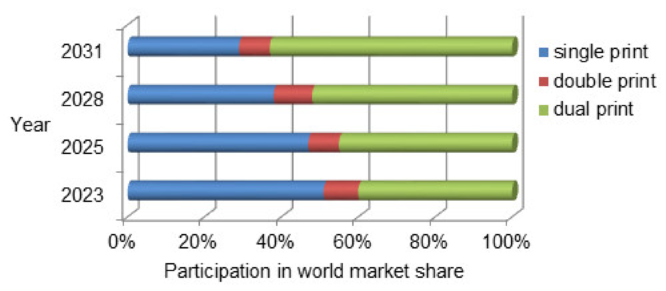
In the case of a template, printing is easy. A template with a given shape is placed directly on the selected substrate, and, for example, the printed paste is pressed through the holes in the pattern with a squeegee (fabric, piece of wood). After removing the template, a printed pattern remains on the surface, representing the template [9,20]. We can be found in the literature the following printing methods: double print, which is known as print on print; the single print, which is understood as one screen print process for the whole metallization, as well dual print process, which is printed separately in two different printing processes both busbars and paths. Figure 3 shows predictions for using these methods for the deposit of silver pastes in the coming years. Although the share using the single print method will decrease, it will continue to have a significant market share. In comparison, the double print method will have a small impact on the market share of no more than 15%.
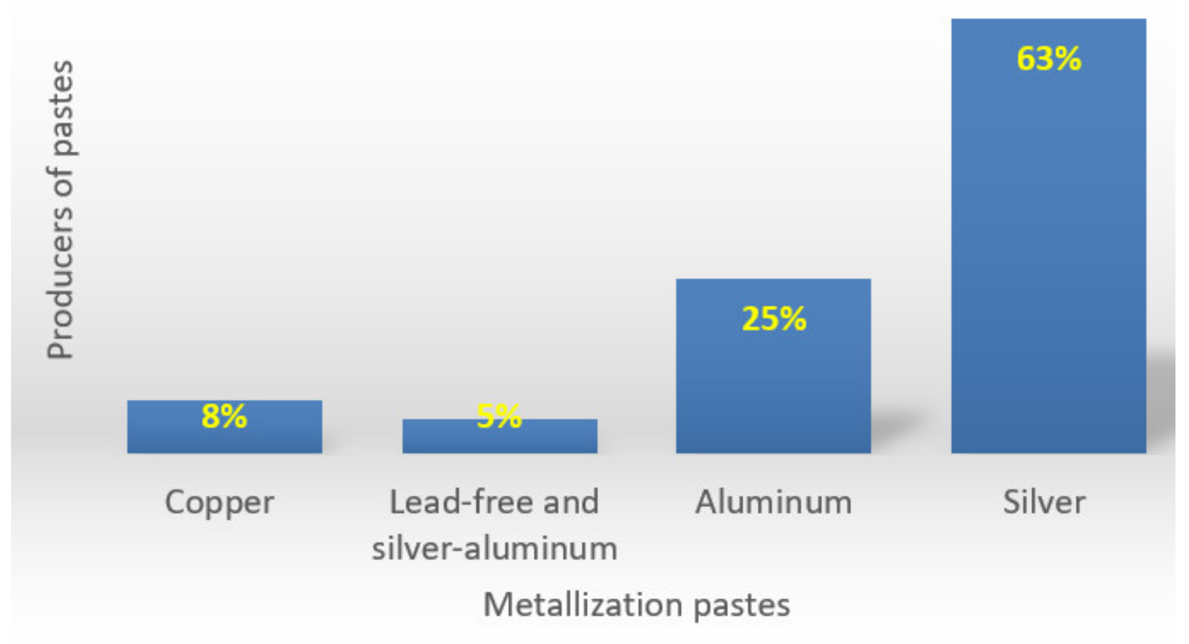
Compared to screen printing, new laser technology is quickly becoming one of the most promising and best alternative track application techniques. Laser technology in producing solar cells is becoming a necessary element of the modern, essential part of an automated operation in producing photovoltaic cells. Some examples involve the fabrication of front metallization using laser methods presented in available literature [16,21,22,23]. Solar cell technology is achieved using an advanced approach like selective emitter structures with the laser beam LDSE (Laser-doped Selective Emitter) [24]. More advanced solar cell concepts include [25] metal or emitter wrap-through (MWT/EWT) [26,27], laser-fired contacts (LFC) [28] or interdigitated back contact (IBC) [29]. We can also find in the literature works on the optimization of metallization grids (for instance, the geometry) [30,31]. Of particular importance is the proper selection of the material of the electrode and substrate. Based on the data in [32], it is possible to find precisely 56 companies involved in the product of metallization paste, one of the essential supply items for PV cell producers. Based on Figure 4, we find information that the most significant number of companies producing silver paste (more than 60%) and the smallest number of copper paste (less than 8%).
Currently, the photovoltaic market, specifically the part of the market responsible for pastes, is dynamically developing to help the customer and thus better adapt the offer to their expectations and requirements. Improving the efficiency of solar cells requires the application of low-temperature pastes in hetero-junction technology, manufacturing contact with emitters of high sheet resistance, reducing the consumption of paste applied for front and the rear connecting contacts, and applying advanced printing technologies (for example, dual printing is increasingly being implemented into production) [33].

3. Application of ALD and PVD Methods

The second of the current research directions is the deposition of conductive emitter coatings in photovoltaic structures using the ALD method, a variant of the CVD method [5]. The ALD process relies on the sequential release of the precursors in gaseous or liquid form to deposit the coating layer by layer. The first precursor is introduced into the reaction chamber, where it then forms a monolayer on the surface of the substrate. The chamber is then purged with an inert carrier gas (usually nitrogen or argon) to remove unreacted precursors and reaction by-products, and another precursor is introduced into the chamber to form another layer, followed by purging again [34]. The described phenomena are successive stages of one ALD cycle (Figure 5), and the entire coating process consists of many such cycles.
Among the characteristic features of the ALD method are the sequentially of the process and the self-limiting rate of layer growth. The former is based on the fact that the chemical precursors are introduced alternately into the growth chamber, and after each introduction of the reactant, the chamber is purged with an inert gas. Consequently, the combination of precursors occurs only at the surface of the substrate, unlike in the classical CVD method, where the reactants are introduced simultaneously, and the reactions between them occur in the gas phase. Thus, the ALD technique’s layers are more homogeneous [35].
The coating application process consists of many cycles [34,35,36,37,38]. The ALD method can be used to deposit [36]:
  • Single elements, e.g., from group IV of the periodic table,
  • Binary compounds, e.g., metal oxides,
  • Multi -component compounds, e.g., hydroxyapatite.
The precursors in the ALD process should have the following characteristics [39]:
  • Volatility —gas pressure >0.1 Tr at <200 °C, liquid at evaporation temperature without decomposition,
  • Reactivity —they can react quickly with the substrate and the other precursor in a self-limiting manner (most are air-sensitive),
  • Stability -the precursor must retain physical and chemical properties at high temperatures,
  • By -products-which should not react with the coating and be easy to remove from the reactor chamber,
  • Availability at the lowest possible price.
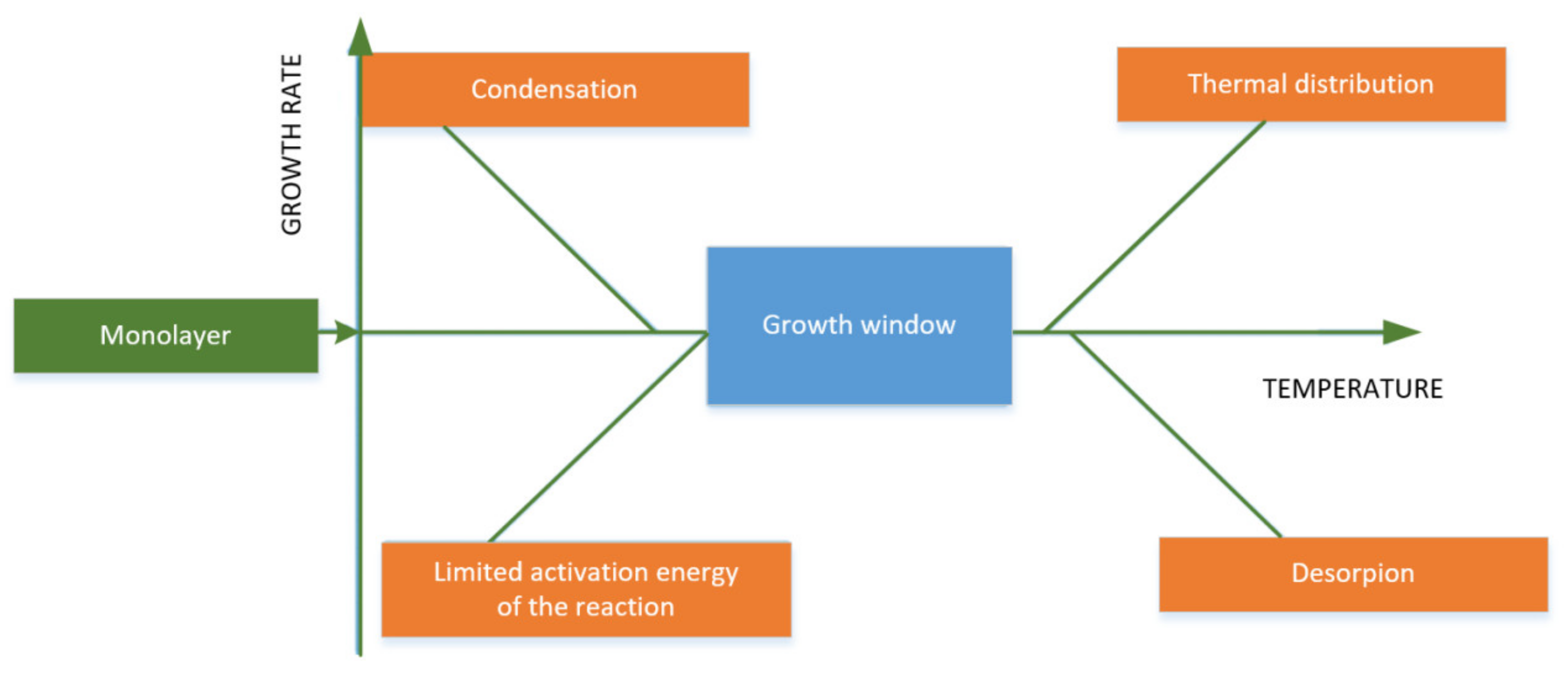
In this process, it is easy to control the growth of the applied layer by controlling technological parameters such as, among others: substrate temperature, time of introducing precursor into the chamber, purging time after each reagent, the precursor temperature, and the number of cycles. The temperature is the most critical parameter that allows controlling the surface coverage directly. ALD processes occur at low temperatures below 350 °C [34,39,40]. The temperature range in which a saturation effect occurs with layer growth (one monolayer is formed in one cycle) depends on the ALD process in question and is referred to as the “ALD growth window”. The temperature outside the “temperature window” generally results in poor growth rates and deposition of non-ALD layers due to low kinetics of the reactions taking place or too much condensation of the precursor on the substrate (at low temperature), or due to thermal decomposition or rapid desorption of the precursor (at high temperature). Schematically, the “growth window” is shown in Figure 6. To achieve the maximum benefits offered by the ALD method, it is crucial to realize the process within the limits of the characteristic “temperature window” [34,36].
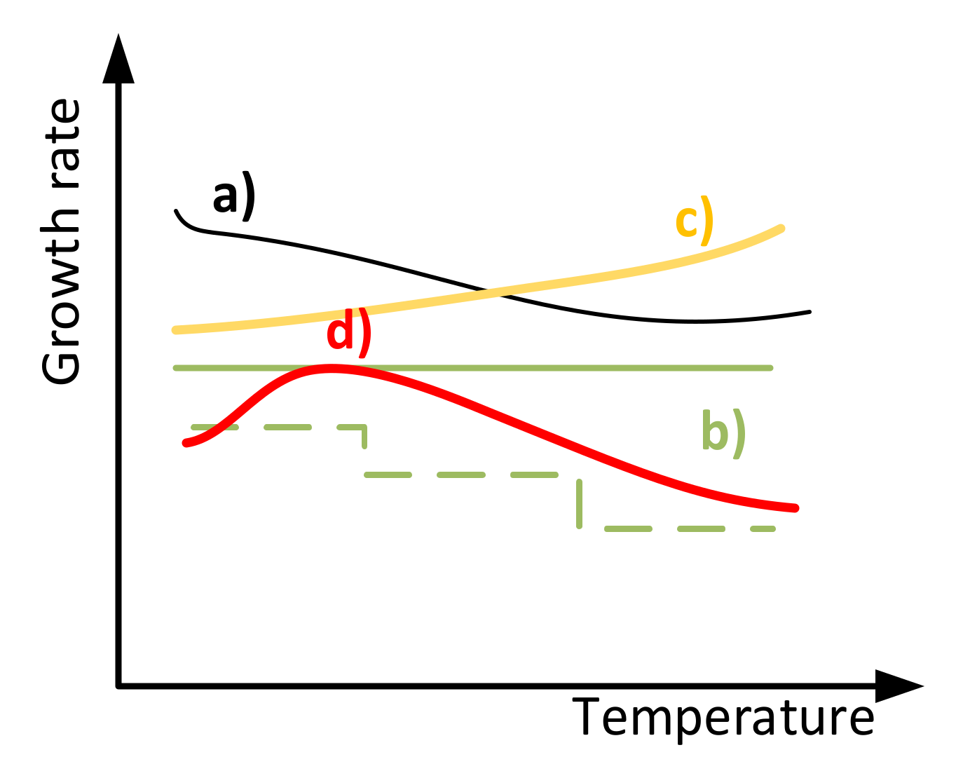
The rate of chemical reactions in the ALD process, and thus the film growth rate, is strongly temperature-dependent and can vary in nature. Diagrams of the possible types of dependencies in the ALD window are shown in Figure 7 [40].
Deposition of ALD thin films is carried out in specially adapted reactors. There are four different types of reactors [39]:
  • With a closed chamber system,
  • With an open chamber system,
  • With a semi-closed chamber system,
  • With a semi-open chamber system.
Currently, the most common type is a closed-chamber reactor. Layers are deposited in a growth chamber (reaction chamber), into which reactants are alternately introduced. Initially, they can be in the solid, liquid, or gas phase. The carrier gas in the process is an inert gas in whose atmosphere the deposition of layers takes place [39].
It can be stated, comparing them to the conventional coating application methods, that they has many advantages (Figure 8), including the possibility of using highly reactive precursors, homogeneity of the obtained layers and control of their thickness, and low surface roughness [39,41,42].
The main disadvantage of the ALD process is the limited range of materials that cannot be highly reactive and the selection of precursors characterized by low activation energy to prevent the thermo-degradation of the substrates [41]. The ALD process is time-consuming because the coating is created from many ultra-thin layers. The required thickness of the coating is obtained by repeating ALD cycles many times (even tens of thousands of times). The typical growth rate of the achieved layer is 100 to 300 nm per hour. Using specially designed reactors, it is possible to increase the deposition rate to 1–2 µm/h. On the macroscopic scale, the process can be related to laminated coatings; however, the ALD process does not use adherents [41]. The coating materials used in the ALD process are extensive (Table 2), and the obtained layers may be [39]: single-element, two-component compounds, or multi-component compounds. Using ALD technology, it is possible to obtain mono-crystalline, polycrystalline, or amorphous layers.

4. Use of TCO in a Photovoltaic Structure

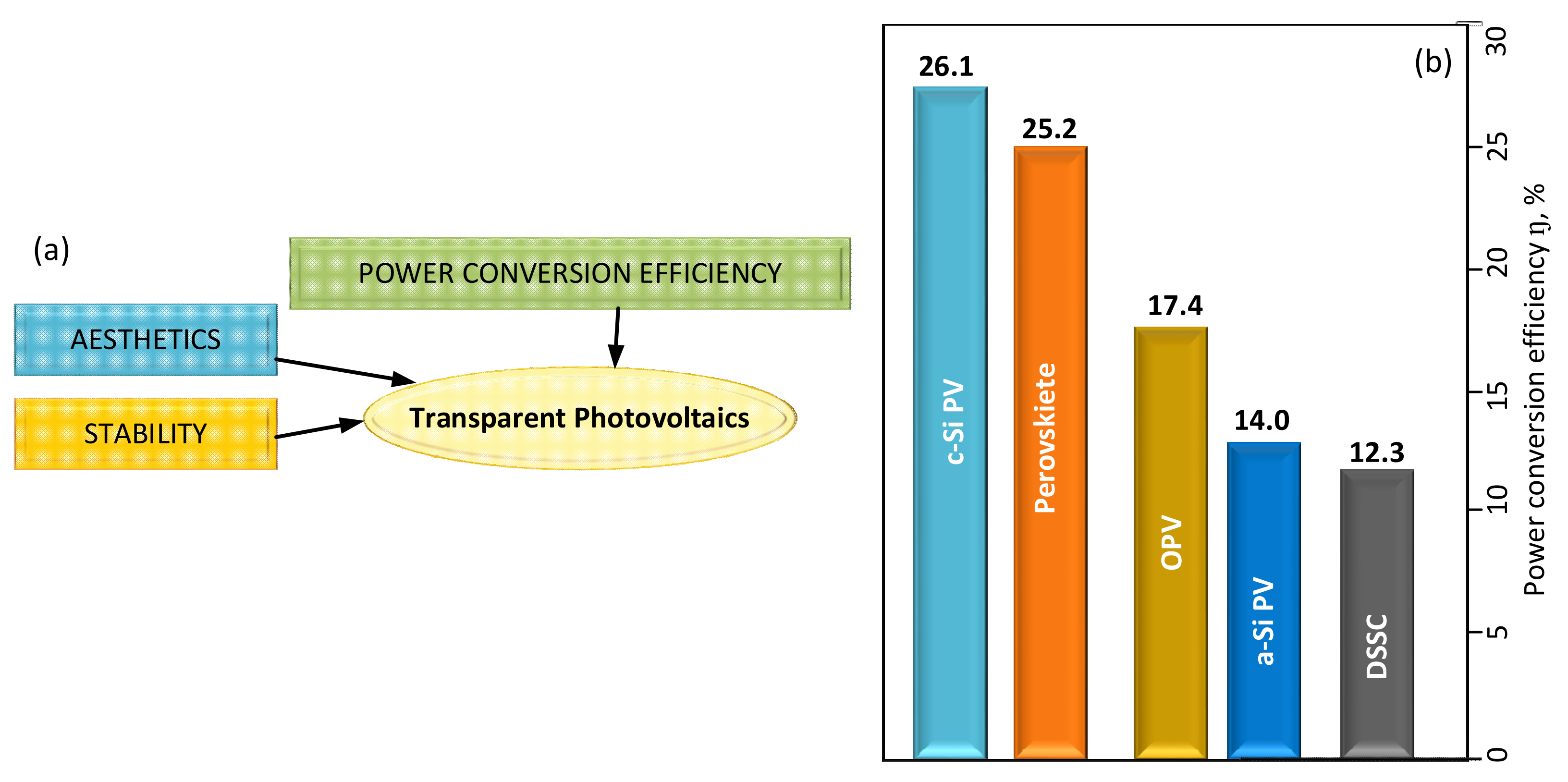
The third of the current research directions is related to transparent semiconductor oxides. For several years, this has been an exciting area of interest for many scientists and research centers [44]. These materials are of particular interest to the field of optoelectronics and photovoltaics [45]. This is confirmed by the report [46], which includes classifying common features of both domains (Figure 9a). These include aesthetics, consistency in their use worldwide, and increased efficiency of photovoltaic cells with the same average visible light transmittance. Figure 9b shows the high photoconversion efficiency of cells based on crystalline silicon and perovskite, which was 26.1% and 25.2%, respectively. The efficiency mentioned above exceeds 25%, and similar values are also observed in the research on transparent photovoltaics. In [47], we can also find that for a perovskite solar cell, the high conversion efficiency was obtained equal to 22.6%; however, in [48], its record photoconversion efficiency was 25.7%. Moreover, the highest lab efficiency in thin film technology is 23.4% for CIGS and 21.0% for CdTe solar cells.
In [47], we find information about record lab cell efficiency for mono-crystalline and multi-crystalline silicon wafer-based technology (26.7% and 24.4%). In 2040, it is predicted that passivated emitter and rear Cells (PERC) made from c-Si and PV cells with aluminium back surface field (BSF) will be among the most prevalent solar cells in mass production using thick-film technology, which is used to produce electronic devices/modules [47].
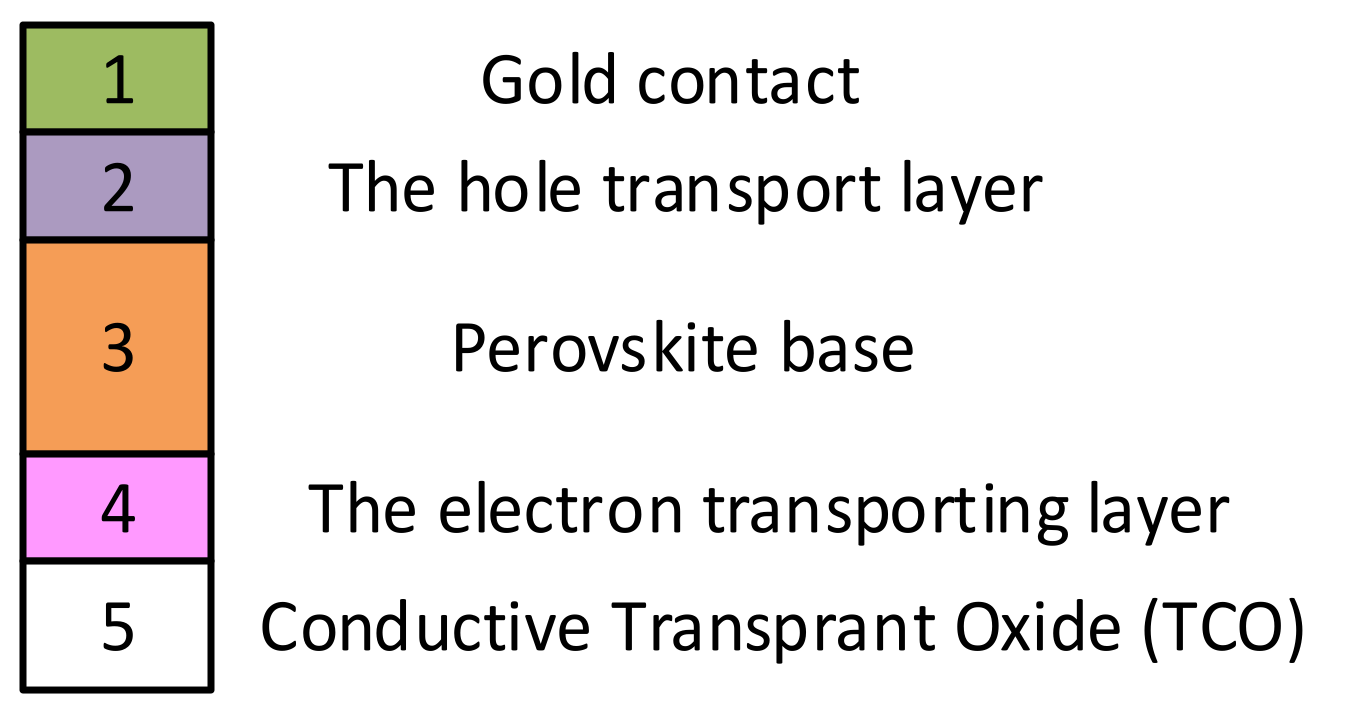
In the case of optical tests, transmittance should be taken into account when analyzing the efficiency of the photovoltaic conversion of a cell. The transmittance should be considered an essential parameter with the photovoltaic conversion efficiency since the efficiency changes with it. Electronically conductive transparent layers are generally obtained based on compounds of indium, tin and zinc doped with tin [48,49]. Indium Tin Oxide (ITO) and Aluminium-doped Zinc Oxide (AZO) will be used in this work; therefore, they will be discussed later. The high transparency of 85–90%, conductivity above 1000 S/cm, charge carrier density of 1∙1021 carriers/cm3, and mobility of 10–100 cm2/Vs are the essential beneficial properties of ITO commonly known in the literature [50,51,52]. The ITO is often used in organic electroluminescence devices (for instance, thin-film transparent electrodes of liquid crystal displays (LCDs) [49,53,54,55,56,57]. The commercially available ITO targets with different doping contents can be used for the ITO deposition at relatively low temperatures [54,58,59,60]. Al-doped zinc oxide is one of the various indium-free materials, which has been known as one of the most promising materials for replacing ITO in electronic devices, because of its abundance, non-toxicity, high conductivity, high transparency in the visible region, and low costs [61,62]. Zinc oxide (ZnO) thin film, due to its wide range of electrical and optical properties, has become a technologically important material. It has been doped with n-type dopants such as Al, In, Ga, Mg, and B to improve ZnO electrical conductivity, optical properties, and thermal stability by providing the extra electron [63]. AZO thin films have been fabricated by various techniques, such as atomic layer deposition and pulsed laser deposition [64], magnetron sputtering, chemical vapor deposition [65], and solution processing [66,67,68,69]. Fluorine-doped tin oxide (FTO) thin film has been used mainly for electronics devices making technologies, for instance, window layers in solar cells [70], gas sensor devices [71], substrates for electro-deposition [72], and transparent contact in optoelectronic and so on. For photovoltaic applications, TCO can be applied as front electrodes of thin film solar cells because of their excellent electrical properties (4.3 × 10⁻⁴ ω.cm 4.3 × 10⁻⁴ ω.cm) combined with high transmission properties (86%) [73]. The paper [74] presented a concept of preparing TCO nanocomposite by combining TCOs and nanoparticles. This example provides guidelines for designing hazy electrodes as light management structures in thin film photovoltaics. FTO is characterized in various technology fields because of its high electrical conductivity, chemical and thermal stability, and optical transparency in the visible range (74). For example, in paper [75], a sol-gel-spin-coating method was used to create a reproducible, scalable, stable, transparent, and conducting tin fluorine-doped indium oxide thin film (FTIO thin film). The method reduced sheet resistance by more than 53% (≤7 ± 1 Ω/sq) of the initial sheet resistance. Pulsed laser deposition [76], chemical vapor deposition (CVD) [77], and sol-gel and spray pyrolysis deposition (SPD) [78]—are just some of the methods used to prepare TCO [79]. Figure 10 shows an example of a PV structure and the use of TCO in this structure.
The issue of TCO was analyzed based on data from the Elsevier (Science Direct), Web of Science, and Scopus databases [80,81,82]. Based on Table 3, it can be concluded that the Elsevier database recorded the highest number of published papers. The Scopus database was second, and WOS was third regarding issues analyzed (state of knowledge as of 7.09.22).
Table 4 summarizes the results of specific issues in the two databases, WOS and Scopus, as of 2020. Analyzing the results obtained, it can be concluded that a higher number of published papers related to issues related to SnO2 is contained in the WOS database than in Scopus, while a comparable number of publications was found for the issue of “AZO and In2O3” for both databases is contained in the WOS database and Scopus. The issue “FTO and In2O3” contains the WOS database than Scopus (state of knowledge as of 5 April 2022).
Some discrepancies in the scientific circulation of published research results in scientific journals in the aforementioned bibliographic databases may be due to the emergence of an increasing number of scientific journals that do not consider the low quality of non-scientific publications. Thanks to the development of information technology, bibliographic lists have been transferred to the virtual space, which has given them a new meaning [83].

5. Summary

External operating parameters characterizing electronic instruments (for example, open-circuit voltage (Voc), short-circuit current (Isc), filling factor (FF), and photovoltaic conversion efficiency (Eff) are the values depending on the material and physical parameters of their separate layers and structural elements [84,85]. The elements and functional layers of an electronic device based on crystalline silicon (c-Si) include an impurity layer forming the emitter of the device, a passivating layer, an anti-reflective coating (ARC), and a front and rear electrode [78,85]. The electronic device’s final operating parameters also determine the base material’s parameters: the starting crystalline silicon wafer, the essential properties of resistivity and the lifetime of minority charge carriers. Consequently, only the mutual combination of the parameters of the base material, the parameters of the layers, and the functional elements of the instrument allows for obtaining an electronic device with the highest quantum efficiency value available for a given set of output parameters [78,85].
Production technologies and the application of surface layers have a stable position and are regarded as basic knowledge in the field of material engineering. In light of the analysis of the literature review, the authors set out two new directions worthy of attention for further research. Further work will require, as appropriate: determining the properties of thin TCO layers applied on silicon substrates by the ALD method for application as conductive emitter coatings in engineering structures, development of engineering structures based on silicon substrates with TCO layers and front contacts, development of a technology for applying a thin layer of TCO on a silicon substrate. According to the requirement of EU Directive 2009/28/EC of the European Parliament and the Council, the increase in the use of renewable energy sources (RES) in the final energy balance will be up to 20% in 2030. Thus, the direction of actions taken in the implementation doctorate is consistent with the implementation of the Polish Energy Policy until 2030 [10].
In sum, the implementation of significant achievements in the coming decade is in line with the fundamental guidelines for the development of photovoltaics as a result of [10,46,78] for the development of guidelines for metallization processes and TCO layers deposited by the ALD method.

Author Contributions

Conceptualization, M.M.-S., writing—original draft preparation M.M.-S. and writing—review and editing, M.M.-S., A.C. and R.R.; supervision, A.C. All authors have read and agreed to the published version of the manuscript.

Funding

Publication supported by the Rector’s pro-quality grant. Silesian University of Technology, grant number 10/050/RGJ22/1028.

Institutional Review Board Statement

Not applicable.

Informed Consent Statement

Not applicable.

Data Availability Statement

Not applicable.

Conflicts of Interest

The authors declare no conflict of interest.

References

  1. Znajdek, K.; Sibiński, M. Postępy w Fotowoltaice; Wydawnictwo Naukowe PWN: Warsaw, Poland, 2021; pp. 60–74. (In Polish) [Google Scholar]
  2. Linie, których Nie widać Zrewolucjonizują Branżę Fotowoltaiczną. Available online: https://magazynfotowoltaika.pl/linie-ktorych-nie-widac-zrewolucjonizuja-branze-fotowoltaiczna (accessed on 22 August 2022).
  3. VDMA. International Technology Roadmap for Photovoltaics (ITRPV), 12th ed.; VDMA: Frankfurt, Germany, 2020. [Google Scholar]
  4. SolarPower Europe. Available online: https://www.solarpowereurope.org (accessed on 22 August 2022).
  5. Dobrzański, L.A.; Pakuła, D.; Staszuk, M. Chemical Vapor Deposition in Manufacturing. In Handbook of Manufacturing Engineering and Technology; Nee, A.Y.C., Ed.; Springer: Berlin/Heidelberg, Germany, 2014; Chapter 30; pp. 2755–2803. [Google Scholar]
  6. Drive, P.H. Laser systems and Processes within Next Generation Photovoltaic Manufacturing Equipment. In Proceedings of the 4th Photovoltaic Manufacturing Technology Conference, Stuttgart, Semicon Europe, Stuttgart, Germany, 8–9 October 2008. [Google Scholar]
  7. Musztyfaga-Staszuk, M. SLS: One of the Modern Technologies of Laser Surface Treatment. Int. J. Thermophys. 2017, 38, 130. [Google Scholar] [CrossRef]
  8. Mertens, K. Photovoltaics: Fundamentals, Technology, and Practice, 2nd ed.; Wiley-Blackwell: Columbia, MD, USA, 2018. [Google Scholar]
  9. Cui, Z. Printed Electronics: Materials, Technologies and Applications; Higher Education Press: Beijing, China, 2016. [Google Scholar]
  10. Directive 2009/28/EC of the European Parliament and of the Council. Available online: https://eur-lex.europa.eu/LexUriServ/LexUriServ.do?uri=OJ:L:2009:140:0016:0062:en:PDF (accessed on 1 August 2022).
  11. Metz, A.; Fischer, M.; Trube, J. Crystalline silicon Technology—Current Status and Outlook. In International Technology Roadmap for Photovoltaics (ITRPV), 8th ed.; PV Manufacturing in Europe Conference Brussels; VDMA: Frankfurt, Germany, 2017. [Google Scholar]
  12. Mat Desa, M.K.; Sapeai, S.; Azhari, A.W.; Sopian, K.; Sulaiman, M.Y.; Amin, N.; Zaidi, S.H. Silicon back contact solar cell configuration: A pathway towards higher efficiency. Renew. Sustain. Energy Rev. 2016, 60, 1516–1532. [Google Scholar] [CrossRef]
  13. Kopecek, R.; Koduvelikulathu, L.J.; Cabrera, E.; Rudolph, D.; Buck, T. The technology with highest efficiency gain potential for c-Si cells. Photovolt. Int. 2015, 4, 52–60. [Google Scholar]
  14. Ralph, E.L. Recent advancements in low-cost solar cell processing. In Conference Record, Proceedings of the 11th IEEE Photovoltaic Specialists Conference, Scottsdale, AZ, USA, 6–8 May 1975; Institute of Electrical and Electronic Engineers: Piscataway, NJ, USA, 1975; pp. 315–316. [Google Scholar]
  15. Burgelman, M. Thin film solar cells by screen printing technology. In Proceedings of the Workshop Microtechnology and Thermal Problems in Electronics, Lodz, Poland, 21–27 September 1998; pp. 129–135. [Google Scholar]
  16. Shanmugama, V.; Cunnusamy, J.; Khanna, A.; Boreland, B.M.; Mueller, T. Optimisation of Screen-Printed Metallisation for Industrial High-Efficiency Silicon Wafer Solar Cells. Energy Procedia 2013, 33, 64–69. [Google Scholar] [CrossRef] [Green Version]
  17. Hamer, D.W.; Biggers, J.V. Technologia Układów Scalonych Grubowarstwowych; WNT: Warsaw, Poland, 1976. (In Polish) [Google Scholar]
  18. Muszyfaga-Staszuk, M. New Copper-Based Composites for the Production of Silicon Photovoltaic Cells; WNT: Warsaw, Poland, 2019; (In Polish). ISBN 978-83-7880-626-4. [Google Scholar]
  19. Hannebauer, H.; Schimanke, S.; Falcon, T.; Altermatt, P.P.; Dullweber, T. Optimised stencil print for low Ag paste consumption and high conversion efficiencies. Energy Procedia 2015, 67, 108–115. [Google Scholar] [CrossRef] [Green Version]
  20. Caballero, L.J. Contact Definition in industrial silicon solar cells. In Solar Energy; Rugescu, R.D., Ed.; IntechOpen: London, UK, 2010; pp. 375–398. [Google Scholar]
  21. Kofron, V.K. Photovoltaic Cell with Junction-Free Essentially-Linear Connections to Its Contacts. U.S. Patent 4,153,907, 8 May 1979. [Google Scholar]
  22. Neuhaus, A.R.; Bultman, J.H.; Tip, A.C.; Sinke, W.C. Metallisation patterns for interconnection through holes. Sol. Energy Sol. Cells 2001, 65, 347–353. [Google Scholar]
  23. Alemán, M.; Streek, A.; Regenfuβ, P.; Mette, A.; Ebert, R.; Exner, H.; Glunz, S.W.; Willeke, G. In Laser micro-sintering as a new metallisation technique for silicon solar cells. In Proceedings of the 21st European Photovoltaic Solar Energy Conference, Dresden, Germany, 4–8 September 2006. [Google Scholar]
  24. Edwards, M. Efficiencies of 22% at low cost: The future of mass-produced laser-doped selective emitter solar cells. Photovolt. Int. 2011, 1, 56–62. [Google Scholar]
  25. Hendell, R. Laser Applications in Solar Cell Manufacturing. In Focus: Laser Micro-Processing; Wiley-VCH: Weinheim, Germany, 2008. [Google Scholar]
  26. Dross, F.; Van, K.E.; Allebe, C.; Van der Heide, A.; Szlufcik, J.; Agostinelli, G.; Choulat, P.; Dekkers, H.F.W.; Beaucarne, G. Impact of Rear-Surface Passivation on MWT Performances. In Conference Record, Proceedings of the IEEE 4th World Conference on Photovoltaic Energy Conversion, Waikoloa, HI, USA, 7–12 May 2006; Institute of Electrical and Electronic Engineers: Piscataway, NJ, USA, 2006. [Google Scholar]
  27. Kerscharer, E.V.; Beaucarne, G. Back-contact Solar Cells: A review. Progress in Photovoltaic: Research and application. Prog. Photovolt. Appl. 2005, 14, 107–123. [Google Scholar] [CrossRef]
  28. Gautero, L.; Hofmann, M.; Rentsch, J.; Lemke, A.; Mack, S.; Seiffe, J.; Nekarda, J.; Biro, D.; Wolf, A.; Bitnar, B.; et al. All-screen-printed 120-µm-thin large-area silicon solar cells applying dielectric rear passivation and laser-fired contacts reaching 18% efficiency. In Proceedings of the 34th IEEE Photovoltaic Specialists Conference (PVSC), Philadelphia, PA, USA, 7–12 June 2009. [Google Scholar]
  29. Neuhaus, D.H.; Münzer, A. Industrial silicon wafer solar cells. Adv. Opto Electron. 2007, 2007, 24521. [Google Scholar] [CrossRef] [Green Version]
  30. Nande, A.; Raut, S.; Dhoble, S.J. Energy Materials. In Perovskite Solar Cells; Dhoble, S.J., Thejo Kalyani, N., Vengadaesvaran, B., Arof, A.K., Eds.; Elsevier: Amsterdam, The Netherlands, 2021; Chapter 9; pp. 249–281. [Google Scholar]
  31. Yang, D.; Zhang, X.; Hou, Y.; Wang, K.; Ye, T.; Yoon, J.; Wu, C.; Sanghadasa, M.; Liu, S.; Priya, S. 28.3%-efficiency perovskite/silicon tandem solar cell by optimal transparent electrode for high efficient semitransparent top cel. Nano Energy 2021, 84, 105934. [Google Scholar] [CrossRef]
  32. Metallization Paste Manufacturers. Available online: https://www.enfsolar.com/directory/material/metallization_paste?tech=408 (accessed on 15 June 2022).
  33. TaiyangNews Provides Update on Latest Technical and Product Solutions to Contact All Types of Solar Cells. Available online: https://taiyangnews.info/reports/market-survey-metallization-pastes-201920/ (accessed on 10 April 2022).
  34. Johnson, R.W.; Hultqvist, A.; Bent, S.F. A brief review of atomic layer deposition: From fundamentals to applications. Mater. Today 2014, 17, 236–246. [Google Scholar] [CrossRef]
  35. Staszuk, M.; Pakuła, D.; Reimann, Ł.; Król, M.; Basiaga, M.; Mysłek, D.; Kří, A. Structure and Properties of ZnO Coatings Obtained by Atomic Layer Deposition (ALD) Method on a Cr-Ni-Mo Steel Substrate Type. Materials 2020, 13, 4223. [Google Scholar] [CrossRef] [PubMed]
  36. Lujala, V.; Skarp, J.; Tammenmaa, M.; Suntola, T. Atomic layer epitaxy growth of doped zinc oxide thin films from organometals. Appl. Surf. Sci. 1994, 82/83, 34–40. [Google Scholar] [CrossRef]
  37. Osadzanie Warstw Atomowych (ALD). Available online: http://www.eagle-regpot.eu/EfI/index.php?pid=33 (accessed on 1 August 2022).
  38. Wojcik, A.; Kiecana, M.; Kopalko, K.; Godlewski, M.; Guziewicza, E.; Yatsunenko, S.; ÃLusakowska, E.; Minikayev, R.; Paszkowicza, W.; Swiatek, K.; et al. Magnetic, structural, and optical properties of low-temperature ZnMnO grown by atomic layer epitaxy; Proceedings of the XXXIV International School of Semiconducting Compounds. Acta Phys. Pol. A 2005, 108, 915–921. [Google Scholar] [CrossRef]
  39. Robertson, J. High dielectric constant oxides. Eur. Phys. J. Appl. Phys. 2004, 28, 265–291. [Google Scholar] [CrossRef] [Green Version]
  40. Boryło, P.; Szindler, M.; Lukaszkowicz, K. Various Applications of Multifunctional Thin Films with Specific Properties Deposited by the ALD Method; Trans Tech Publications: Wollerau, Switzerland, 2019; pp. 111–123. [Google Scholar]
  41. Provine, J.; Rincon, M. Atomic Layer Deposition: Introduction to the Theory and Cambridge Nanotech Savannah & Fiji; Stanford University: Stanford, CA, USA, 2012. [Google Scholar]
  42. Poortmans, J.; Pieters, P.; Baert, K. Exploiting the microelectronics toolbox to boost Si PV manufacturing. Photovolt. Int. 2011, 3, 102–110. [Google Scholar]
  43. Grochowski, J.; Guziewicz, M.; Borysiewicz, M. Analiza transmisji optycznej półprzewodnikowych warstw NiO osadzanych metodą magnetronowego rozpylania katodowego. Elektron. Konstr. Technol. Zastos. 2011, 52, 7. (In Polish) [Google Scholar]
  44. Lee, K.; Kim, N.; Kim, K.; Um, H.-D.; Jin, W.; Choi, D.; Park, J.; Park, K.J.; Lee, S.; Seo, K. Neutral-Colored Transparent Crystalline Silicon Photovoltaics. Joule 2020, 4, 235–246. [Google Scholar] [CrossRef]
  45. Fraunhofer Institute for Solar Energy Systems (ISE). Photovoltaics Report; Prepared with support of PSE Conferences &Consulting GmbH; Fraunhofer Institute for Solar Energy Systems: Freiburg im Breisgau, Germany, 2021. [Google Scholar]
  46. NREL-Led Research into Perovskite-Silicon Tandem Cells Shows New Path to Take. Available online: https://www.nrel.gov/news/program/2020/nrel-led-research-into-perovskite-silicon-tandem-cells-shows-new-path.html (accessed on 11 August 2022).
  47. Kryłow, J.; Oleński, J.; Sawicki, Z.; Tumański, A. Domieszkowanie Półprzewodników, Procesy Technologiczne w Elektronice Półprzewodnikowej; WN: Warsaw, Poland, 1980. (In Polish) [Google Scholar]
  48. Vlooswijk, A. Growth & Characterisation of p-Type Transparent Oxide Semiconductors. Master’s Thesis, Applied Physics, Inorganic Materials Science, Faculty of Science and Technology, University of Twente, Enschede, The Netherlands, February 2005. [Google Scholar]
  49. Klein, E.; Hubert, K.; Paul, O.; Ruther, P. Low-temperature plasma annealing of sputtered indium tin oxide for transparent and conductive thin-films on glass and polymer substrates. Thin Solid Films 2020, 693, 137715. [Google Scholar] [CrossRef]
  50. Hamberg, I.; Granqvist, C.G. Evaporated Sn-doped In2O3 films: Basic optical properties and applications to energy-efficient windows. J. Appl. Phys. 1986, 60, R123–R159. [Google Scholar] [CrossRef]
  51. Laist, J.W. Copper, Silver and Gold, 2nd ed.; D. van Nostrand Company: Toronto, ON, Canada, 1954. [Google Scholar]
  52. Ross, R.B. Copper Cu. In Metallic Materials Specification Handbook; Springer: Boston, MA, USA, 1992. [Google Scholar]
  53. Bartsch, J.; Mondon, A.; Bayer, K.; Schetter, C.; Hörteis, M.; Glunz, S.W. Quick Determination of Copper-Metallization Long-Term Impact on Silicon Solar Cells. J. Electrochem. Soc. 2010, 157, H942. [Google Scholar] [CrossRef]
  54. Minami, T. Present status of transparent conducting oxide thin-film development for Indium-Tin-Oxide (ITO) substitutes. Thin Solid Films 2008, 516, 5822–5828. [Google Scholar] [CrossRef]
  55. Tak, Y.H.; Kim, K.B.; Park, H.G.; Lee, K.H.; Lee, J.R. Criteria for ITO (indium-tin-oxide) thin film as the bottom electrode of an organic light-emitting diode. Thin Solid Films 2002, 411, 12–16. [Google Scholar] [CrossRef]
  56. Song, P.K.; Akao, H.; Kamei, M.; Shigesato, Y.; Yasui, I. Preparation and crystallisation of tin-doped and undoped amorphous indium oxide films deposited by sputtering. Jpn. J. Appl. Phys. 1999, 38, 5224–5226. [Google Scholar] [CrossRef]
  57. Nam, E.; Kang, Y.; Son, D.; Jung, D.; Hong, S.; Kim, Y.S. Electrical and surface properties of indium tin oxide (ITO) films by pulsed DC magnetron sputtering for organic light-emitting diode as anode material. Surf. Coat. Technol. 2010, 205, S129–S132. [Google Scholar] [CrossRef]
  58. Minami, T.; Sonohara, H.; Kakumu, T.; Takata, S. Physics of very thin ITO conducting films with high transparency prepared by DC magnetron sputtering. Thin Solid Films 1995, 270, 37–42. [Google Scholar] [CrossRef]
  59. Ellmer, K. Past achievements and future challenges in the development of optically transparent electrodes. Nat. Photonics 2012, 6, 809. [Google Scholar] [CrossRef]
  60. Sun, L.; Grant, J.T.; Jones, J.G.; Murphy, N.R. Tailoring electrical and optical properties of Al-doped ZnO thin films grown at room temperature by reactive magnetron co-sputtering: From bandgap to near-infrared. Opt. Mater. 2018, 84, 146–157. [Google Scholar] [CrossRef]
  61. Ellmer, K.; Bikowski, A. Intrinsic and extrinsic doping of ZnO and ZnO alloys. J. Phys. D Appl. Phys. 2016, 49, 413002. [Google Scholar] [CrossRef]
  62. Wu, Y.; Potts, S.; Hermkens, P.; Knoops, H.; Roozeboom, F.; Kessels, W. Enhanced doping efficiency of Al-doped ZnO by atomic layer deposition using dimethyl aluminium isopropoxide as an alternative aluminium precursor. Chem. Mater. 2013, 25, 4619–4622. [Google Scholar] [CrossRef]
  63. Knoops, H.C.; Loo, B.W.; Smit, S.; Ponomarev, M.V.; Weber, J.-W.; Sharma, K.; Kessels, W.M.; Creatore, M. Optical modeling of plasma-deposited ZnO films: Electron scattering at different length scales. J. Vac. Sci. Technol. 2015, 33, 021509. [Google Scholar] [CrossRef] [Green Version]
  64. Zhang, H.; Li, X.; Fang, Z.; Yao, R.; Zhang, X.; Deng, Y.; Lu, X.; Tao, H.; Ning, H.; Peng, J. Highly conductive and transparent AZO films fabricated by PLD as source/drain electrodes for TFTs. Materials 2018, 11, 2480. [Google Scholar] [CrossRef] [PubMed] [Green Version]
  65. Shahid, M.; Deen, K.; Ahmad, A.; Akram, M.; Aslam, M.; Akhtar, W. Formation of Al-doped ZnO thin films on glass by sol-gel process and Characterisation. Appl. Nanosci. 2016, 6, 235–241. [Google Scholar] [CrossRef]
  66. Islam, M.R.; Rahman, M.; Farhad, S.; Podder, J. Structural, optical and photocatalysis properties of sol-gel deposited Al-doped ZnO thin films. Surf. Interfaces 2019, 16, 120–126. [Google Scholar] [CrossRef]
  67. Nasiri, M.; Rozati, S. Muscovite mica as a flexible substrate for transparent conductive AZO thin films deposited by spray pyrolysis. Mater. Sci. Semicond. Process. 2018, 81, 38–43. [Google Scholar] [CrossRef]
  68. Stapiński, T.; Godlewski, M.; Jakubowska, M.; Marszałek, K.; Pietruszka, R.; Panek, P.; Soliński, B.; Soliński, I.; Turoń, K.; Wróblewski, G. Materiały i Metody Optymalizacji Budowy Ogniw i Paneli Fotowoltaicznych; AR TOP: Kraków, Poland, 2014; pp. 15–77. [Google Scholar]
  69. Luque, A.; Hegedus, S. (Eds.) Handbook of Photovoltaic Science and Engineering; John Wiley & Sons, Ltd.: New York, NY, USA, 2003. [Google Scholar]
  70. Chae, J.; Kim, D.Y.; Kim, S.; Kang, M. Photovoltaic efficiency on dye-sensitised solar cells (DSSC) assembled using Ga-incorporated TiO2 materials. J. Ind. Eng. Chem. 2010, 16, 906–911. [Google Scholar] [CrossRef]
  71. Hossein-Babaei, F.; Amini, A. A breakthrough in gas diagnosis with a temperature-modulated generic metal oxide gas sensor. Sens. Actuators B Chem. 2012, 166–167, 419–425. [Google Scholar] [CrossRef]
  72. Khelladi, M.; Mentar, L.; Boubatra, M.; Azizi, A.; Kahoul, A. Early stages of cobalt electro-deposition on FTO and n-type Si substrates in sulphate medium. Mater. Chem. Phys. 2010, 122, 449–453. [Google Scholar] [CrossRef]
  73. Muthukumar, A. Fluorine-doped tin oxide (FTO) thin film as transparent conductive oxide (TCO) for photovoltaic applications. AIP Conf. Proc. 2013, 1512, 710. [Google Scholar]
  74. Nazeeruddin, M.K.; Baranoff, E.; Grätzel, M. Dye-sensitised solar cells: A brief overview. Sol. Energy 2011, 85, 1172–1178. [Google Scholar] [CrossRef]
  75. Kadam, A.N.; Chowdhury, S.R.; Bathula, C.; Kumar, N.; Kumar, V.; Jha, M.K.; Lee, S.-W.; Misra, M. A novel reduction approach for fabrication of transparent conducting fluorine and tin-doped indium oxide thin film with low sheet resistance. Ceram. Int. 2022, 48, 29307–29313. [Google Scholar] [CrossRef]
  76. Chen, Z.; Lai, J.; Shek, C. Multifractal spectra of scanning electron microscope images of SnO2 thin films prepared by pulsed laser deposition. Phys. Lett. 2005, 345, 218–223. [Google Scholar] [CrossRef]
  77. Fang, T.-H.; Chang, W.-J. Effect of freon flow rate on tin oxide thin films deposited by chemical vapour deposition. Appl. Surf. Sci. 2003, 220, 175–180. [Google Scholar] [CrossRef]
  78. Moholkar, A.; Pawar, S.; Rajpure, K.; Bhosale, C. Effect of solvent ratio on the properties of highly oriented sprayed fluorine-doped tin oxide thin films. Mater. Lett. 2007, 61, 3030–3036. [Google Scholar] [CrossRef]
  79. Napi, M.L.M.; Maarof, M.F.; Soon, C.F.; Nayan, N.; Fazli, F.I.M.; Hamed, N.K.A.; Mokhtar, S.M.; Seng, N.K.; Ahmad, M.K.; Suriani, A.B.; et al. Fabrication of fluorine-doped tin oxide (FTO) thin films using spray pyrolysis deposition method for transparent conducting oxide. J. Eng. Appl. Sci. 2016, 11, 8800–8840. [Google Scholar]
  80. Web of Science (Clarivate). Available online: https://www.webofscience.com/ (accessed on 7 September 2022).
  81. SCOPUS. Available online: https://www.scopus.com (accessed on 7 September 2022).
  82. Elsevier (Science Direct). Available online: https://www.sciencedirect.com/ (accessed on 7 September 2022).
  83. Indeksowanie Czasopism w Referencyjnych Bazach Danych. Available online: https://depot.ceon.pl/bitstream/handle/123456789/15614/Aneta_Drabek_Indeksowanie_czasopism_w_referencyjnych_bazach_danych.pdf?sequence=1&isAllowed=y (accessed on 6 September 2022).
  84. Boxwell, M. Solar Electricity Handbook: A Simple, Practical Guide to Solar Energy—Designing and Installing Solar Photovoltaic Systems, 2022 ed.; Greensteram Publishing: Birmingham, UK, 2022. [Google Scholar]
  85. Zalewski, E.F.; Geist, J. Solar cell spectral response characterisation. Appl. Opt. 1979, 18, 3942–3947. [Google Scholar] [CrossRef]
Figure 1. The market dominance of single-double-sided contact concepts [3].
Energies 15 09026 g001
Figure 2. The trend for remaining silver per PV cell for chosen concept p-type (front and rear side of PV cell, where value for cell size are 166 and 166 mm2) [3].
Energies 15 09026 g002
Figure 3. Prediction of the use of various front contact printing methods [3].
Energies 15 09026 g003
Figure 4. Market survey on metallization pastes [32].
Energies 15 09026 g004
Figure 5. ALD cycle diagram.
Energies 15 09026 g005
Figure 6. Temperature dependence of layer growth rate [36].
Energies 15 09026 g006
Figure 7. Dependence of growth rate on the temperature in the ALD window: (a) with increasing temperature, the growth rate decreases; (b) the growth rate is constant; (c) with increasing temperature, the growth rate increases; (d) the growth rate decreases with increasing temperature after reaching a maximum value [40].
Energies 15 09026 g007
Figure 8. Comparison of ALD and CVD processes [39,40,41].
Energies 15 09026 g008
Figure 9. The perspective of the development of transparent photovoltaics: (a) classification of features, (b) classification of photoconversion efficiency of cells [46].
Energies 15 09026 g009
Figure 10. An example of a planar structure of a perovskite-based photovoltaic cell [1].
Energies 15 09026 g010
Table 1. Technology development in various areas of the photovoltaic industry [4].
NoApplication Criteria Specific Tasks to Be Performed
1AbsorberDevelopment of performed research on contamination and technical defects of modules/panels
Development of thinner and larger wafer areas for more efficient use
Development of new passivation techniques
2Photovoltaic cellsDeveloping lower-cost manufacturing solar cells
Designing high-precision equipment for accurate solar cell processing
Improving anti-reflection layers and light-trapping in the solar cells
3Metal grids (contacts)Reducing surface recombination by minimizing contact surfaces and strong doping under contacts
4InterconnectionDeveloping modern ways of joining solar cells
5PackagingInnovative drive to reduce optical losses
Developing changes in the appearance of modules
Improving inspection systems to detect defects, automatically record their identified class, and reduce them while maintaining high sensitivity, efficiency, and process performance
Developing new materials to reduce the cost of creating modules while maintaining their operational reliability
6ManufacturingOngoing innovation in commercially used products Introducing changes at every stage of production to improve the finished product
Table 2. Materials used to make ALD thin films [34,40,43].
Pure ElementsOxidesNitridesSulfidesCarbidesFluoride
C, Al, Si, Ti, Mn, Fe, Co, Ni, Cu, Zn, Ga, Ge, Mo, Ru, Rh, Pd, Ag, Sb, Ta, W, Os, Ir, PtAl2O3, TiO2, Ta2O5, Nb2O5, Zr O2, HfO2, SiO2, SnO2, In2O2, ZnO, MgO, La2O3, Y2O3, CeO2, Sc2O3, Cr2O3, Er2O3, VO2, B2O3, Co2O3, CuO, Fe2O3, NiO, Ga2O3, WO3,…AlN, TaNx, NbN, TiN, MoN, ZrN, HfN, GaN, WxN, InN, …ZnS, SrS,
CaS, PbS, …
TiC, NbC,
TaC, …
CaF2, SrF2,
ZnF2, …
Table 3. List of issued publications on general topics according to three databases [80,81,82].
Issue SearchedYear WOSSCOPUSELSEVIER
Transparent Conductive Oxides2012–202223828144172814
Table 4. List of publications issued according to two databases with details [80,81].
WOSSCOPUSWOSSCOPUSWOSSCOPUSWOSSCOPUS
AZO and In2O3FTO and In2O3In2O3TCO and In2O3
6638209.1165.710561376
AZO and SnO2FTO and SnO2SnO2TCO and SnO2
2236147840134.25825.305579516
Publisher’s Note: MDPI stays neutral with regard to jurisdictional claims in published maps and institutional affiliations.