Abstract
Currently, the design of resonant power converters has only been developed while operating in the steady state, while the design operating in the transient stage has not been considered nor reported. This paper is interested in testing the performance of the resonant circuits operating in the transient stage and finding applications where benefits can be obtained from this form of operation. One application in which it is possible to obtain benefits from designing resonant circuits in the transient state is in the area of frequency multiplication. Usually, to achieve frequency multiplication, it is necessary to resort to complex methods and special devices that increase the complexity of the design and the total cost of the circuit. This paper evaluates the performance of a series RLC resonant circuit operating in the transient stage and with an underdamped response acting as a frequency multiplier, where the oscillation frequency of the current in the resonant tank is “n” number of times the switching frequency of the square voltage source at the input with a duty cycle of D = 50%. To validate the analysis, a circuit was designed to deliver an output power of 30 watts to a resistive load, where the switching frequency of the square voltage source at the input was 500 kHz. Since a multiplier value “n” equal to fifteen was chosen, the current in the resonant tank reached an oscillation frequency of 7.5 MHz. The design methodology was validated by simulations in SPICE, complying with the established design parameters.
1. Introduction
The development of electronic systems has been constant, with advantages in areas such as switched-mode power supply systems, filters, etc. Currently, designers have focused on reducing cost, size, and increasing energy efficiency to achieve a good use of energy and extend the life of electronic devices [1,2,3]. A good way to achieve these objectives is to operate at high frequencies, as this reduces the size of the components that store energy, which reduces the cost of the total converter and increases the power density [4,5,6,7]. Usually, for these types of applications, resonant converters are the most widely used since they allow working at high frequencies and with soft switching, which greatly reduces switching losses [8,9,10]. The problem with operating at frequencies above 1 MHz is that it usually requires expensive programmable electronic cards, sophisticated semiconductors, and complex control methods applied at the inverter/rectifier stage when frequency multiplication is required. This leads to an increase in the overall circuit cost, complexity, and problems in the electronics, such as negative bias temperature instability, hot carrier injection, etc. [11,12,13,14,15,16,17].
Conventionally, the design of resonant converters is performed in the steady-state and for its analysis, the method called first harmonic approximation is used, which is a modeling technique where it is assumed that only the first harmonic signal contributes to the power transfer [18,19]. The performance of resonant circuits operating in the transient state has not been widely considered, and it is of great interest to see in which applications the analysis of resonant circuits operating in the transient state can be used.
In this work, the analysis and design in the transient state of a series RLC circuit acting as a frequency multiplier are shown, where the oscillation frequency of the current in the resonant tank is equal to “n” times the switching frequency at the input of the circuit (fo = nfsw), which allows operating at high oscillation frequencies in the resonant tank without needing a high switching frequency at the input of the circuit. Frequency multipliers are not a recent topic and multiple works have already been reported. A frequency multiplier is a DC circuit in which the frequency of the output signal is a harmonic component of the frequency of the supply signal; if the frequency of the input signal is “fsw”, a resonant tank can be used to filtrate out the unwanted frequency components and leave only the signal component whose frequency is “nfsw” at the output [20,21]. These circuits are usually used in high-frequency RF applications when parasitic semiconductor components limit the maximum operating switching frequency, such as in switched-mode inverters and power amplifiers [22,23]. These types of frequency multiplication techniques have been proposed in the design of DC-DC converters but are not commonly performed since the output power of a frequency-multiplying inverter is intrinsically low when compared to the ratings of the required devices [24,25,26].
Currently, many methods used in frequency multiplication have been reported: the frequency doubler using the Injection-Locked frequency multiplier technique, which is used to generate a differential signal and increase the power of the second order harmonic component filtered with an LC circuit [27]; the frequency doubler using Schottky diodes where series connected diodes polarized in the output waveguide are used [28]; the frequency tripler using a pair of antiparallel GaAs Schottky diodes where the pair of diodes are used as nonlinear devices to generate harmonic components for the input signal in the Q-band [29]; the frequency tripler by the triple push technique using heterojunction bipolar transistors (HBT) technology, which consist of three identical unit-cell multipliers which are individually pumped by the W-band input signals with 120° phase difference so that the third harmonic components are combined in phase at the output [30]; the frequency doubler and tripler using the Class E amplifier with shunt linear and nonlinear capacitances where it is necessary to select an appropriate value of the shunt capacitor to achieve the frequency multiplication [31]; and finally using the well-known technique called “Variable Frequency Multiplier” (VFX) in which the duty cycle and switching frequency of an inverter or rectifier are modified as the input or output voltages change to create different operating modes, allowing a tripling or quadrupling of the operating frequency [32,33].
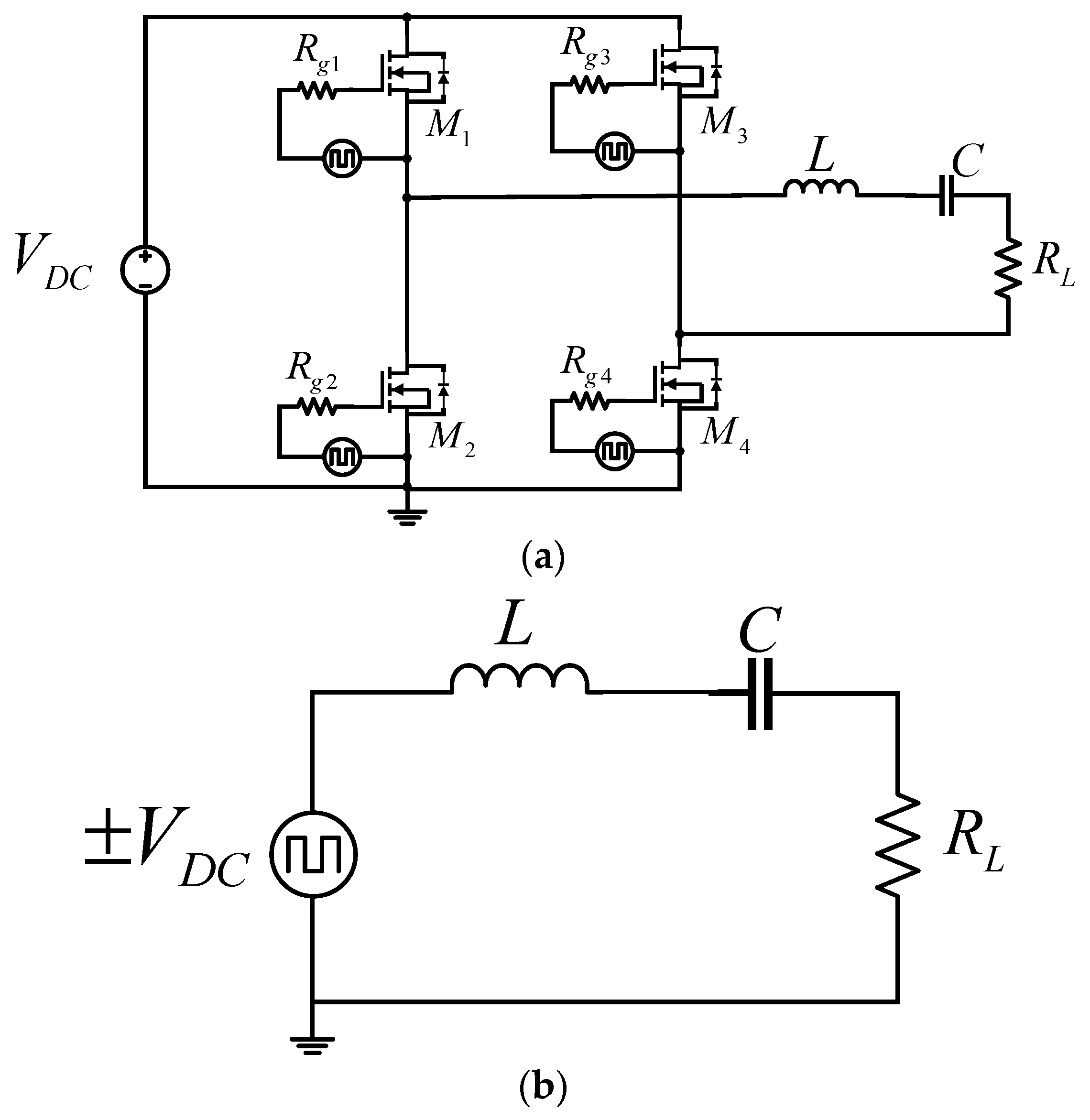
In this work, frequency multiplication is achieved by operating in the transient stage and without the need for special devices or complex control methods, which only raise the overall cost of the circuit and add complexity to the design. It is also possible to work with much higher power levels. This transient design methodology has not been reported before and can be used in applications where high operating frequencies are required without the need to work with very low power levels. As shown in Figure 1, this design methodology could be used in resonant circuits that have an inverter stage that can generate a certain switching frequency, since the inverter output voltage can be replaced by a bipolar square voltage source.

Figure 1.
Design methodology for transient state applied to resonant circuits with inverter stage. (a) Resonant inverter with series RLC circuit. (b) Series RLC equivalent circuit with bipolar voltage source replacing the inverter output voltage.
The proposed design methodology was able to achieve the previously established design parameters, which were verified by simulations in SPICE; however, the performance of the circuit under these operating conditions presented inconveniences, which varied depending on whether the values of “n” are even or odd. These inconveniences were the high supply voltage levels of the circuit and the large instantaneous power peaks demanded from the power supply.
In future work, the design methodology and analysis shown in this paper could be applied to the design of resonant converters which can be used in applications where high operating frequencies are required, such as wireless power transmission, which has become a trend due to many applications that do not involve wired connections [34,35,36,37,38].
2. Analysis of the Circuit
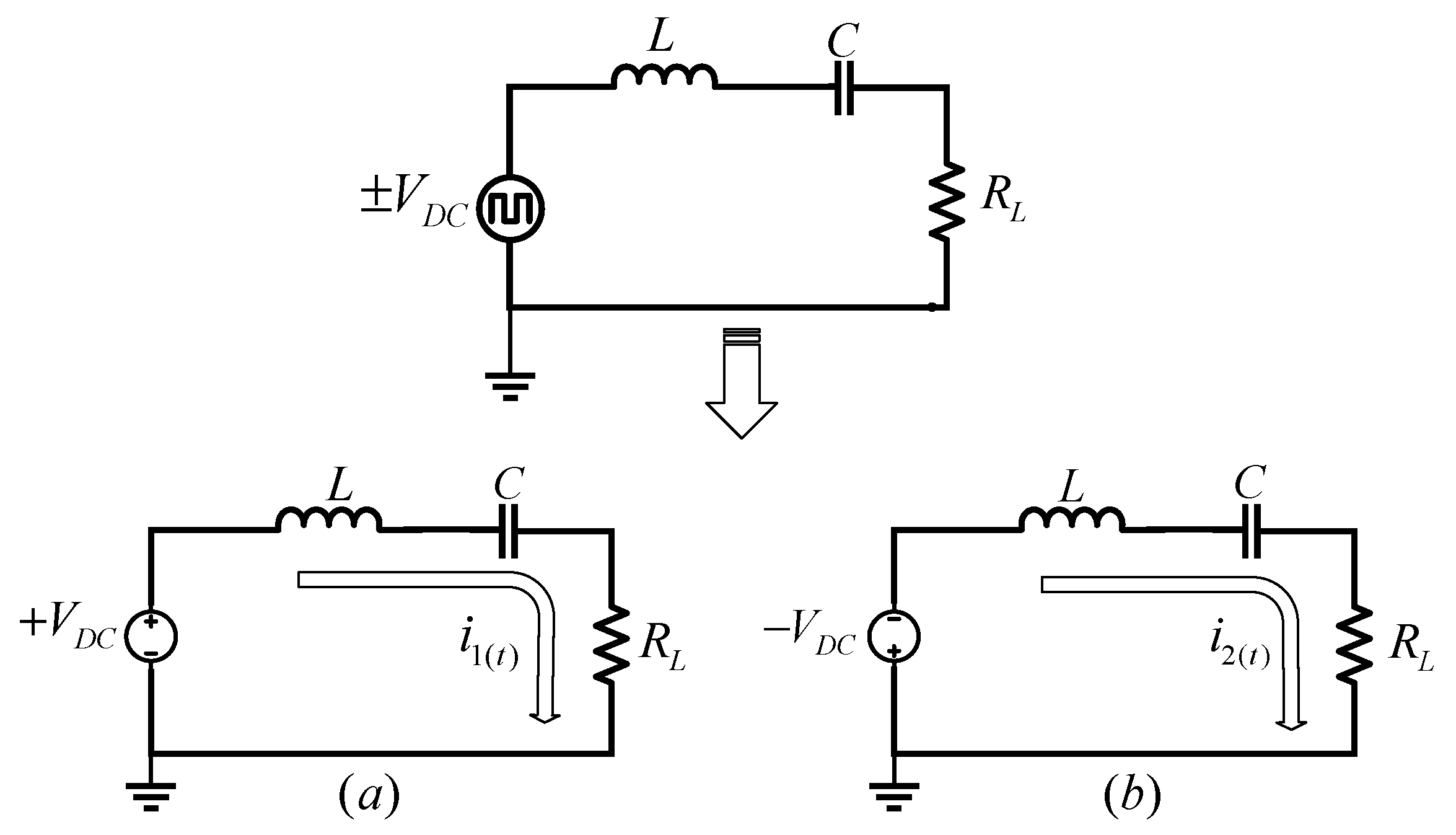
In the following section, the analysis of the circuit operating with an underdamped response is developed. Figure 2 shows the series RLC circuit with a bipolar source at the input, which needs to be analyzed as two circuits with different voltage sources at the input.
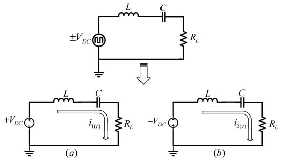
Figure 2.
Series RLC resonant circuit with bipolar square voltage source at the input. (a) Series RLC circuit when the voltage source is positive. (b) Series RLC circuit when the voltage source is negative.
2.1. Determination of the Instantaneous Current with Underdamped Response Circulating in the Resonant Tank
Due to the bipolarity of the voltage source at the input of the circuit, there are two states with different polarities in the input voltage, as shown in Figure 2a,b.
Following the procedure in [39], the differential equation that defines the behavior of the current in the circuits of Figure 2a,b is determined as follows:
Roots of Equation (1):
where:
Considering the circuits shown in Figure 2, two current equations will be obtained for each circuit, defined as:
where i1(t) represents the current flowing in circuit Figure 2a with +VDC, i2(t) represents the current flowing in circuit Figure 2b with −VDC, and T is the switching period of the bipolar voltage source at the input. In the analysis, it is necessary to consider the duty cycle of 50% because a sinusoidal current waveform with symmetry in the two states of the circuit is sought. This consideration is usually taken into account in the design of conventional resonant converters. Another consideration in the design of the underdamped circuit was that in both states of Figure 2 the capacitor voltage during switching would be equal to the supply voltage multiplied by a constant “c”, as shown in Equation (4).
Considering Equation (4), the solution of Equation (1) is determined to find the equation that defines the behavior of the current in the circuits of Figure 2a,b. As it is known, the solution for the case where the current has an underdamped response (ωo > α) is defined by Equation (5), where it is necessary to determine the value of the constants K1 and K2.
where β is defined in Equation (6). The procedure for determining the values of the constants in Equation (5) is not new and can be found in detail in [40]. To reduce Equation (5) into known terms, β is replaced by ωo considering the following:
where represents the constant that defines the level of underdamping of the current in the resonant tank and ωo represents the angular frequency of the current in the resonant tank. In Equation (6), for values of ≥ 10, then:
Substituting the value of the constants (K1, K2) and substituting Equation (7) into Equation (5), the current behavior in the circuits of Figure 2a,b are defined as follows:
2.2. Determination of Parameters Defining the Underdamping Level and Waveform of the Instantaneous Current in the Resonant Tank
As previously mentioned, the objective of this analysis is to multiply the frequency of the current in the resonant tank. Thus, the angular frequency of the current in the resonant tank is considered as:
where n represents the number of times to multiply the resonant frequency “fo” in the resonant tank, fsw is the switching frequency of the bipolar voltage source at the input, and fsw = 1/Ts.
In this paper, the analysis of the RLC circuit will be done only for a duty cycle D = 50%. Therefore, the half period of the bipolar voltage source switching (DTs = ton = T/2) is considered a function of the time constant “τ” and a constant called “k”:
where:
For this analysis, the Euler exponential () of Equation (5) is called the damping factor “df”, which is expressed as a function of the constant “k” and can take values from df = 0.1 to df = 0.9, as shown below:
where k represents the constant that defines the maximum current decay up to half of the switching period (ton = Ts/2), assuming an inverter duty cycle of D = 50%.
The influence of the damping factor “df” on the current waveform (i(t)) is graphically represented in Figure 3. As shown in Figure 3, the damping factor defines how sinusoidal the current waveform is, where, if fully sinusoidal waveforms are required, it is necessary to use high damping factors to prevent the current from decaying significantly, and, where using a damping factor of “df = 0.9” is equivalent to an almost sinusoidal waveform. Figure 3 also shows the exponential factor (), which is the factor that defines the decay of the current up to half of the switching period (T/2). The following is to determine the value of the constant “k” as a function of the circuit parameters:
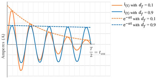
Figure 3.
Influence of the damping factor “df“ in the instantaneous current waveform (i(t)) in the resonant tank: current with less sinusoidal waveform (orange), current with sinusoidal waveform (blue).
Considering the above equations, substituting into Equation (10), and solving for “k”:
Expressing the constant “k” in terms of the constant “a”, which defines the level of underdamping, and the multiplier “n”:
Considering the above equations, substituting and simplifying into Equation (12):
Considering Equation (11), the constant “k” can obtain values that depend on the damping factor as shown below:
Equation (13) obtains the equation that defines the value of the constant “a”. Substituting (14) into (13) and solving for “a”:
where n represents the number of times to multiply the resonant frequency “fo” in the resonant tank. The constant “a” is directly related to the quality factor of the resonant tank. Since a higher level of underdamping increases the quality factor “Q”, the quality factor for this analysis of the series RLC circuit is considered as follows:
where Es represents the maximum stored energy in the inductor, PR the energy dissipated in the resistor, and XL the inductive reactance at the frequency fo. The mathematical demonstration which relates the quality factor “Q” to the constant “a” is shown below:
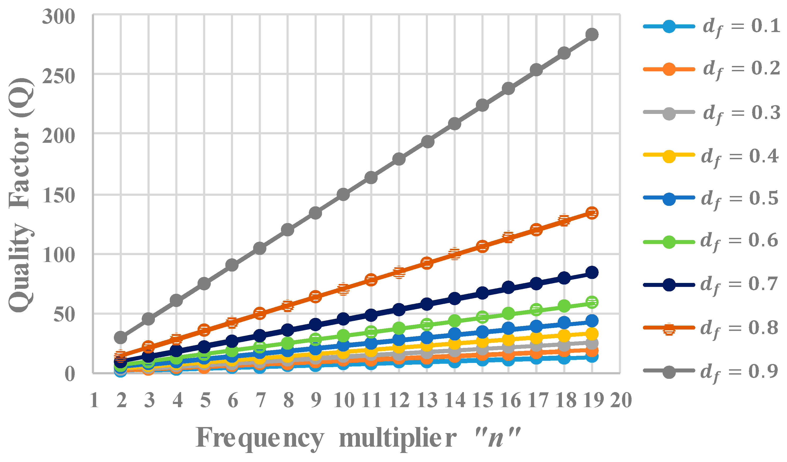
Figure 4 shows the variation of the quality factor by increasing the multiplier “n” for even and odd values with the fixed damping factor “df”.
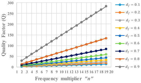
Figure 4.
Quality factor with fixed damping factor “df” for odd and even values of the multiplier “n”.
As shown in Figure 4, increasing the multiplier “n” increases the quality factor “Q”, where the higher the damping factor “df” also generates higher values in the quality factor. From Equation (12), it is possible to determine the value of the time constant “τ” as a function of the duty cycle “D”, the switching frequency “fsw”, and the constant “k” as shown below:
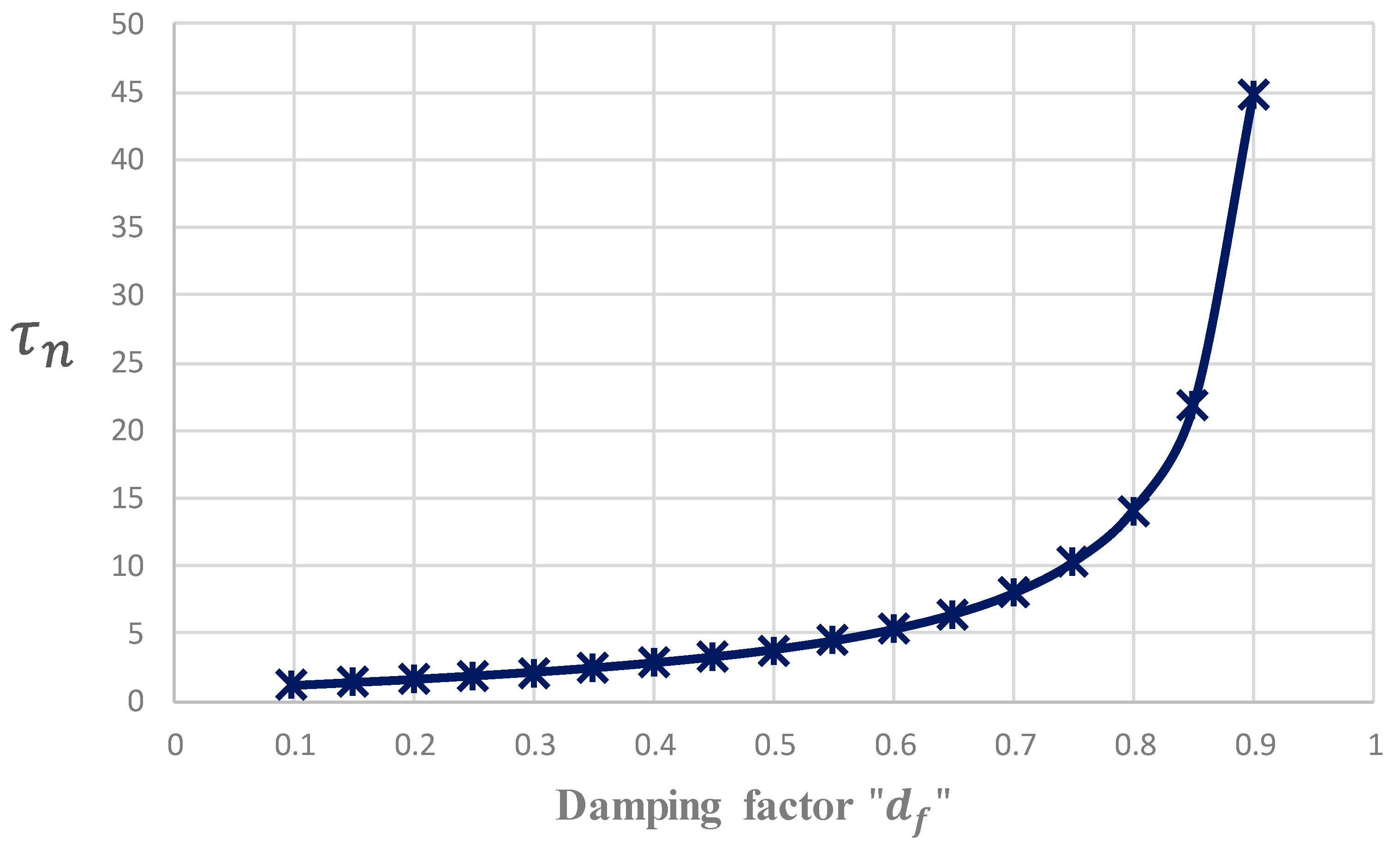
Figure 5 shows the value of the normalized time constant “τn” for different values of the damping factor “df”, where the equation defining the value of the normalized time constant is shown below:
where in the constant “τ” is being considering the minimum value of the damping factor (df = 0.1).
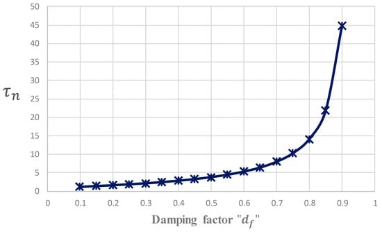
Figure 5.
Value of the normalized tau constant “τn” for different damping factors.
As shown in Figure 5, the value of the normalized tau constant increases as the damping factor increases, indicating that the inductance value “L” only depends on the damping factor “df” and not on the multiplier “n”, since, as shown in Equation (18), the switching frequency “fsw”, the duty cycle “D”, and the load “R” are predefined values that do not change. Figure 5 also shows the number of times the inductance value increases; when using a damping factor of “df = 0.9”, the inductance value increases almost forty-five times compared to using a damping factor of “df = 0.1”. Therefore, high values of the inductance “L” are necessary to obtain sinusoidal current waveforms, where a higher “n” frequency multiplier will not affect the inductance value.
2.3. Determination of the Maximum Current in the Resonant Tank for Even and Odd Values of “n” with the Determination of Constant “c”
As shown in Equation (8), which defines the behavior of the currents i1(t) and i2(t) in the resonant tank, it is necessary to find the value of the constant “c” which defines the maximum value of the current. This constant is found by determining the voltage in the capacitor by integrating the circulating current in the circuit (i1(t), i2(t)) as shown below:
where Imax represents the maximum value of the current, XC the capacitive reactance at the resonant frequency fo, and n the number of times to multiply the resonant frequency in the resonant tank.
Solving Equation (20):
In Equation (21), if the value of “n” is an odd or even number, there will be two equations defining the capacitor voltage. Simplifying and considering that “n” is an EVEN number:
Simplifying and considering that “n” is an ODD number:
As shown in Equation (8), the maximum current in the resonant tank is defined as:
Expressing Equation (24) in known terms:
To determine the constant “c”, it is necessary to separate it from Equations (22) and (23). Since there are two equations of the voltage in the capacitor, there will be two equations that will define the value of the constant “c”. Substituting Equation (25) into (22) and solving for ceven:
Substituting Equation (25) into (23) and solving for codd:
2.4. Determination of the Circuit Operating Parameters
The power at the load is one of the most important parameters to be determined in this circuit, and is defined as follows:
As shown in Equation (28), it is necessary to determine the RMS current in the resonant tank, which is defined as:
Solving Equation (29):
In Equation (30), whether “n” is an odd or even number, the equation in simplified form is as follows:
where b represents the expression in square brackets. Substituting (31) into (28), the equation of the power in the load is as follows:
The supply voltage can be determined by substituting Equation (25) into (32) and solving for VDC:
By manipulating Equation (33), it is possible to determine the gain of the circuit “M” as follows:
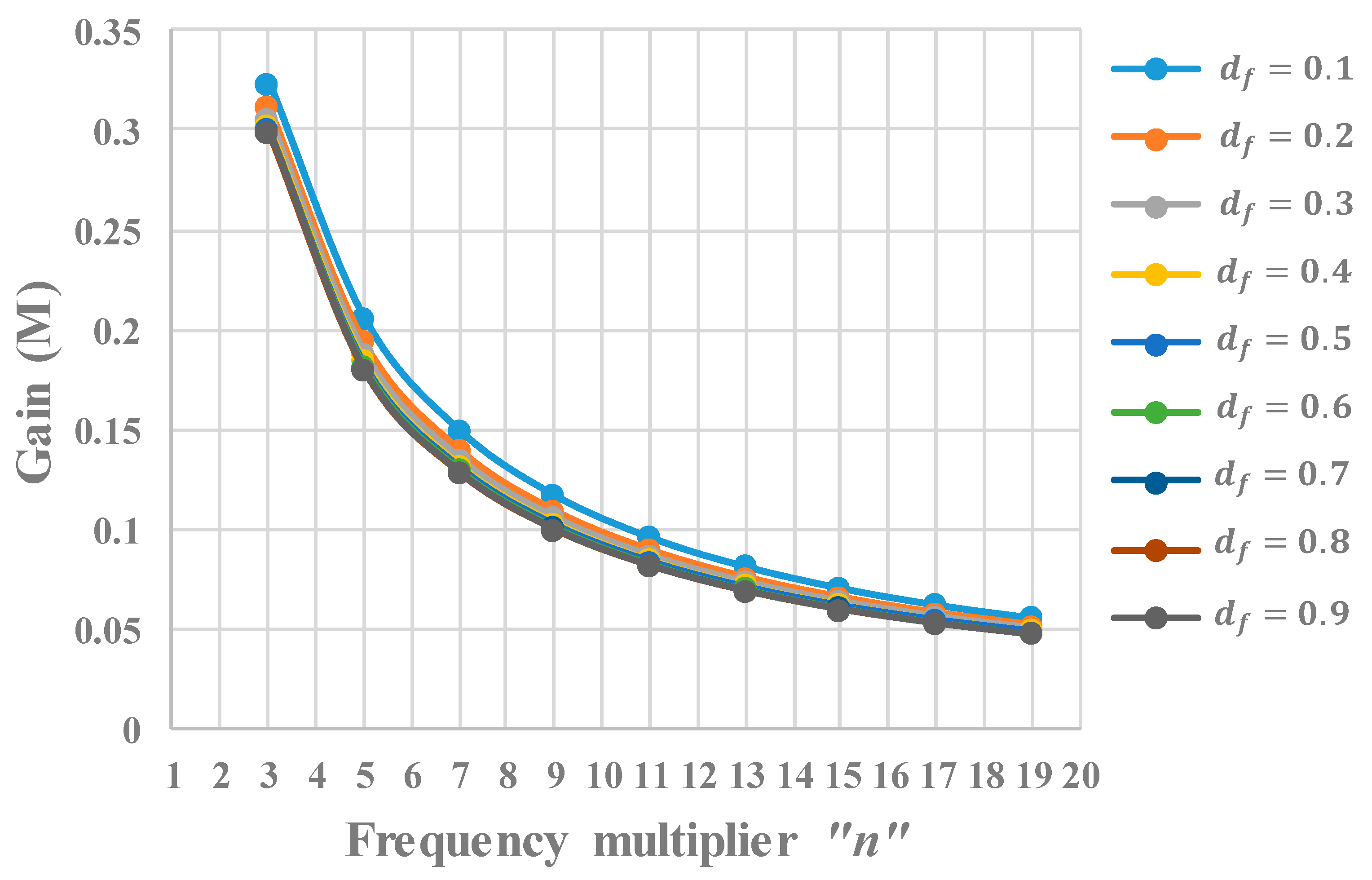
where constant “c” can be for even values “ceven” or odd values “codd”. As shown in Equation (34), the gain of the circuit can vary as a function of the values of the constants “a”, “b”, “c”, and the duty cycle. However, the variation of the duty cycle would affect the current waveform and its symmetry, thus, a fixed value of D = 50% was considered in the circuit analysis. Since two equations define the value of the constant “c”, it is possible to plot the gain of the circuit with odd and even values of “n” for different values of the damping factor “df”. Figure 6 shows the gain of the circuit “M” with even values of “n” and a fixed damping factor. Figure 7 shows the gain of the circuit “M” with odd values of “n” and a fixed damping factor. As shown in Figure 6 and Figure 7, the circuit gain for both cases using even and odd values of “n” tends to decrease as the multiplier increases. As shown in Figure 7, when using odd values of “n”, the circuit gain does not vary significantly when using different values of the damping factor “df”, when compared to using even values of “n” as shown in Figure 6. This difference in gain behavior when using even or odd values of “n” shows that it is convenient to use odd values of “n” since, if a sinusoidal current is required in the resonant tank, a damping factor of “df ≥ 0.9” must be used. Using even values of “n” is less convenient because the gain is very small, as shown in Figure 6.
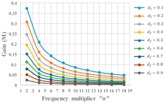
Figure 6.
Gain (M) with even values of “n” and fixed damping factor “df”.
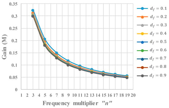
Figure 7.
Gain (M) with odd values of “n” and fixed damping factor “df”.
3. Design Methodology and Simulation
3.1. Design Methodology
To validate the above equations, a design methodology was proposed to test the performance of the series RLC resonant circuit operating in the transient stage with an underdamped response. Table 1 shows the operating parameters of the circuit and Table 2 presents the proposed design methodology for the proposed odd value of “n”.

Table 1.
Circuit design parameters.

Table 2.
Design methodology.
3.2. Simulation of the Circuit
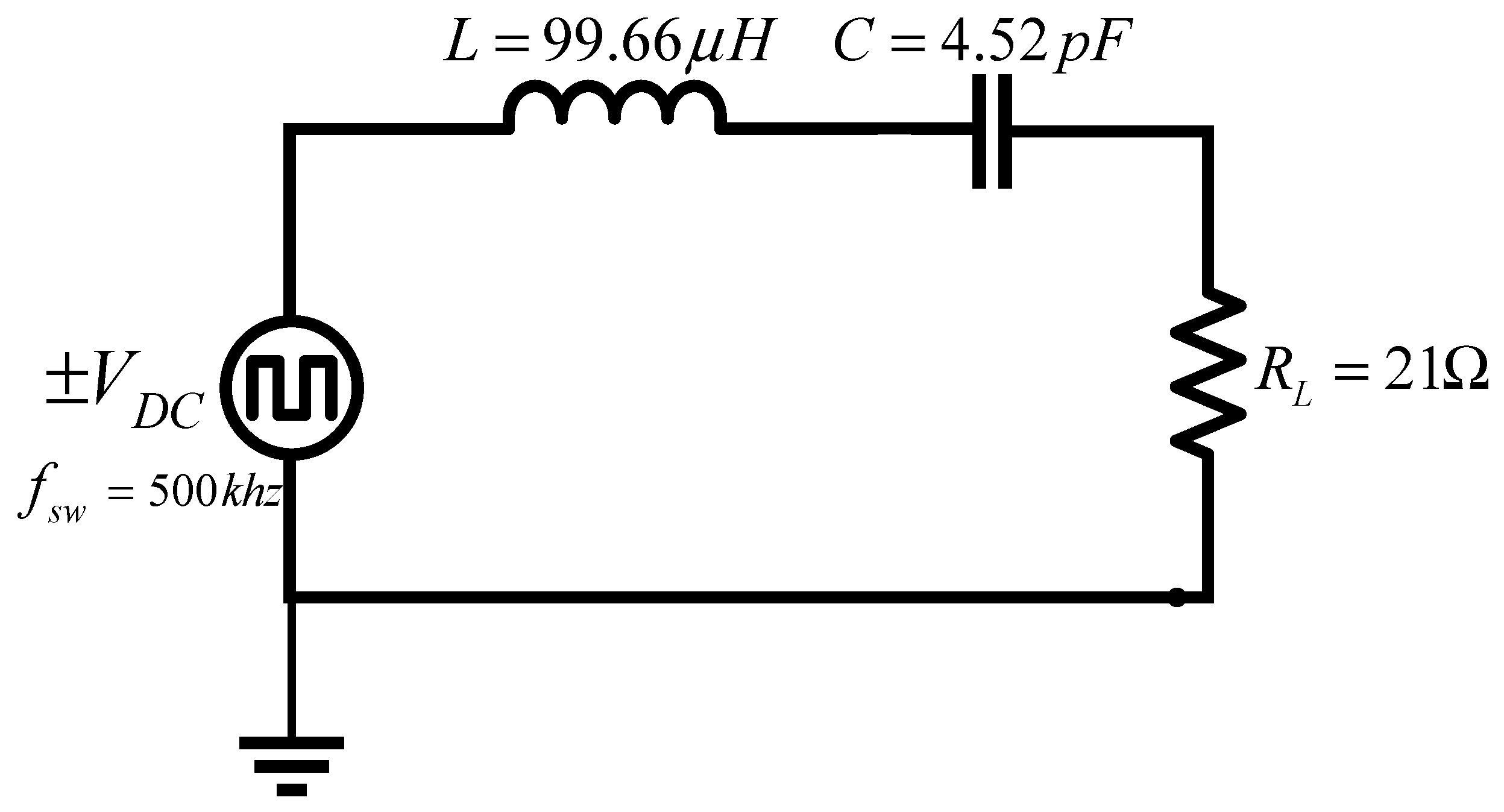
To validate the design methodology, the series RLC resonant circuit shown in Figure 8 was simulated in the software OrCAD PSpice using the values shown in Table 2.
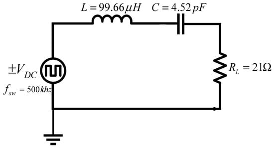
Figure 8.
Series RLC circuit designed in the transient state simulated in OrCAD PSpice.
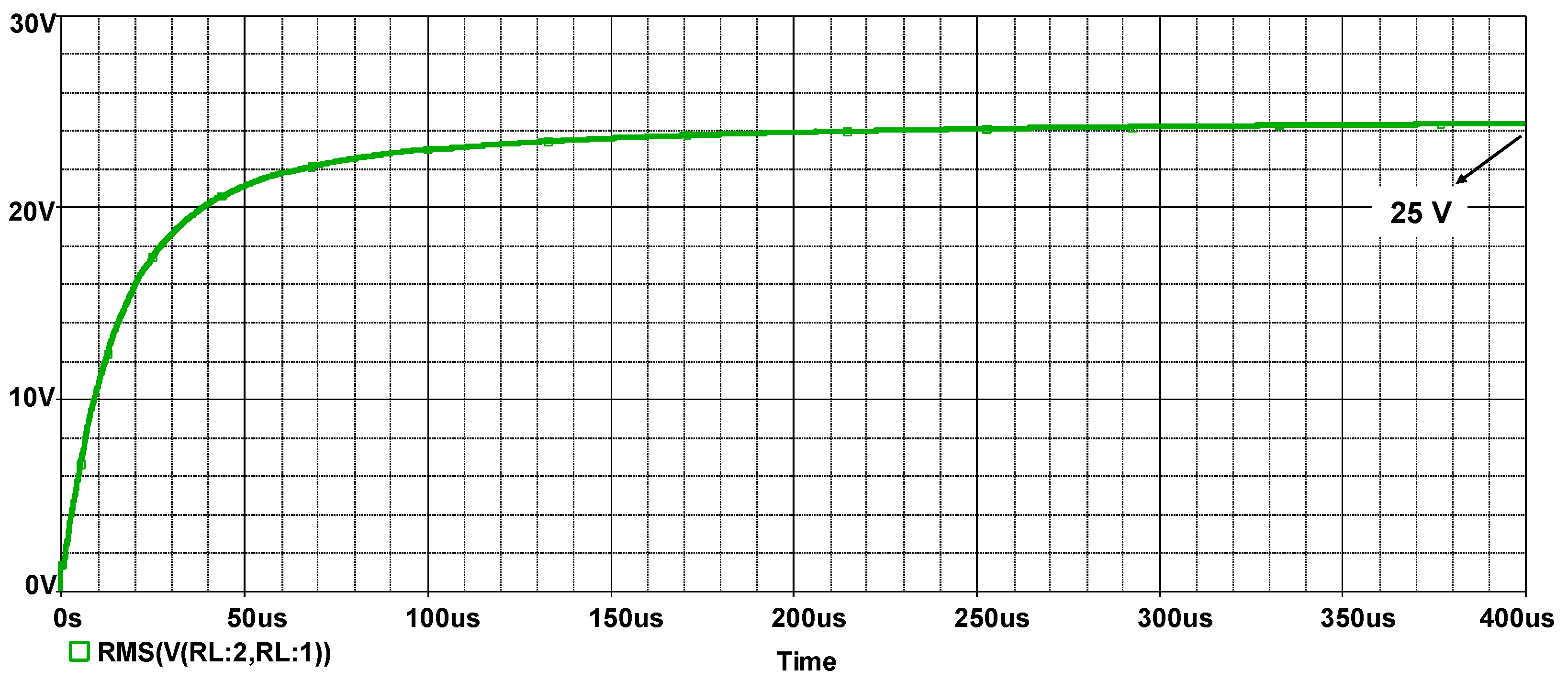
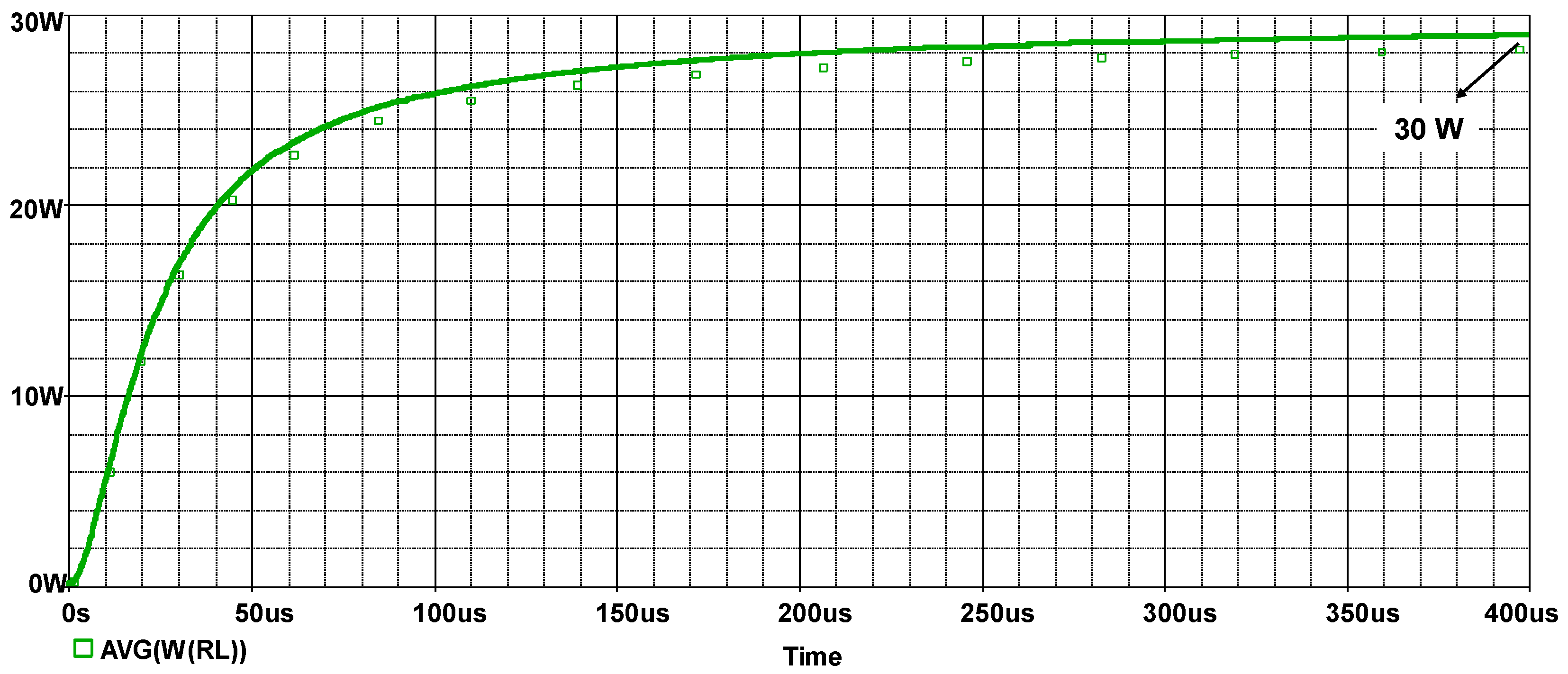
The simulation time was 400 µs, which ensures the stability of the circuit operation. The simulation results are shown in Figure 9, Figure 10, Figure 11, Figure 12, Figure 13 and Figure 14.
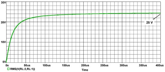
Figure 9.
RMS output voltage (Vout) at the load resistor.
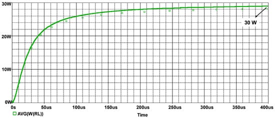
Figure 10.
Average output power (Po) at the load resistor.
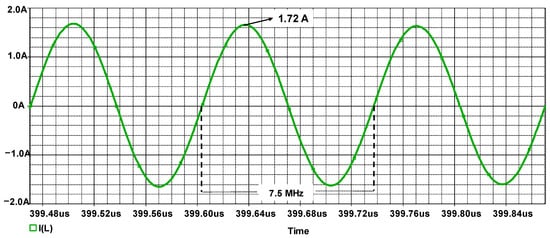
Figure 11.
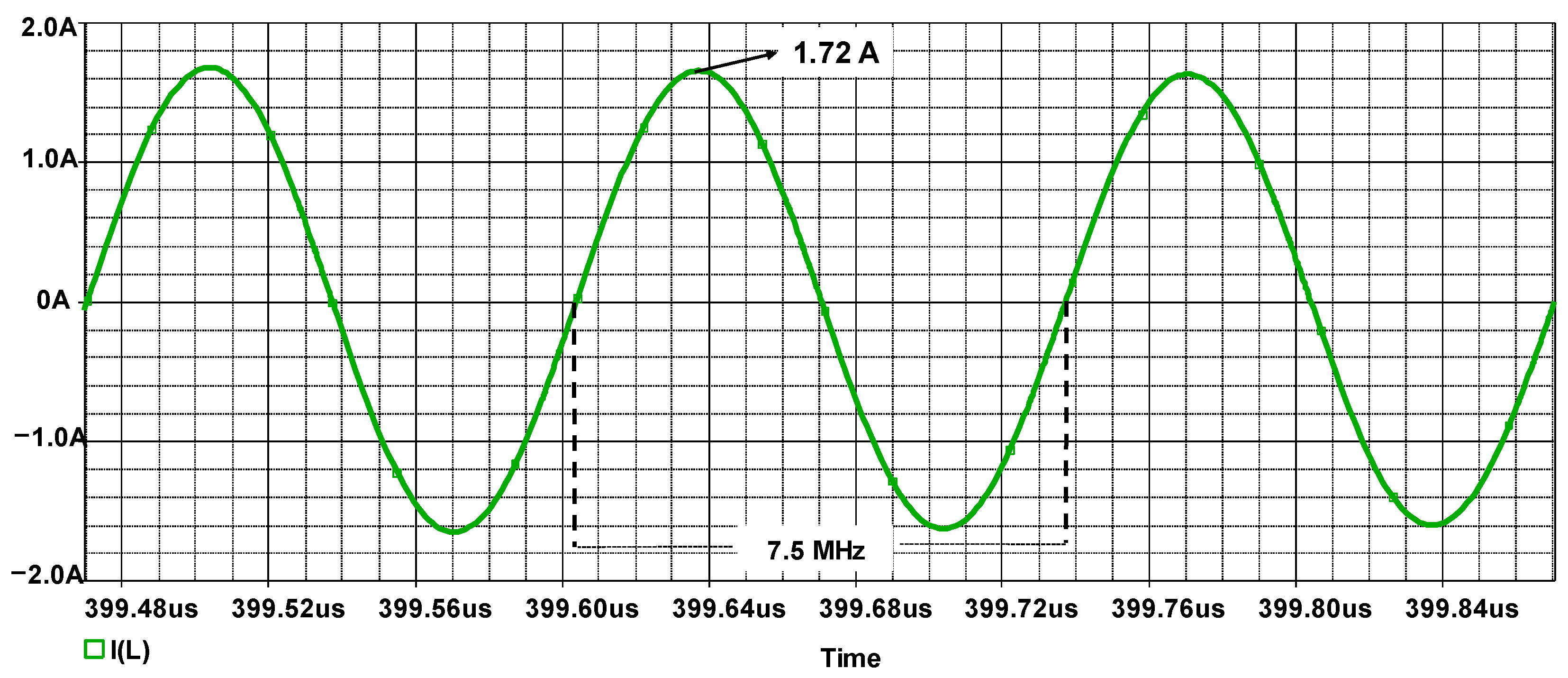
Current in the resonant tank.

Figure 12.
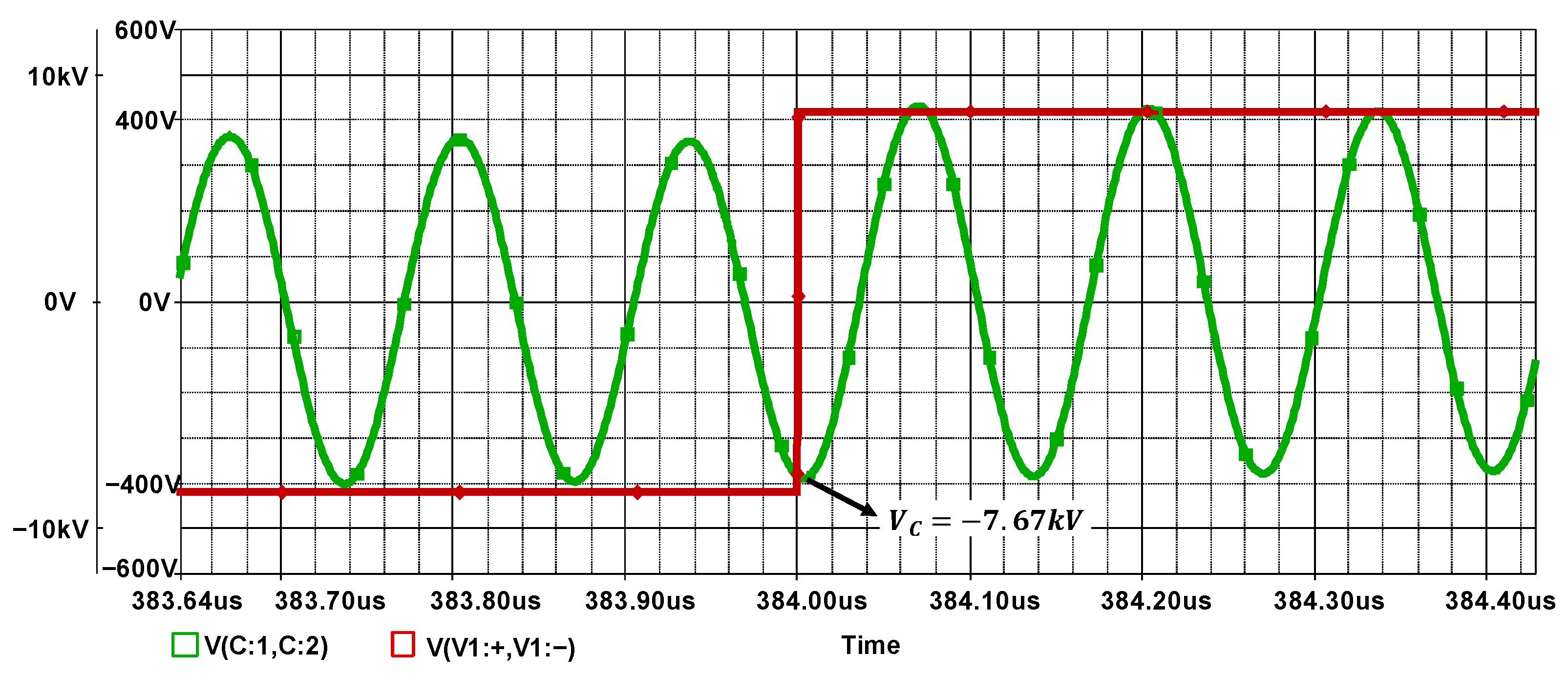
Voltage level on the resonant capacitor in the middle of the switching period (VC = cVDC).
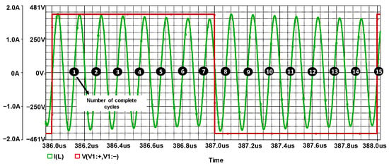
Figure 13.
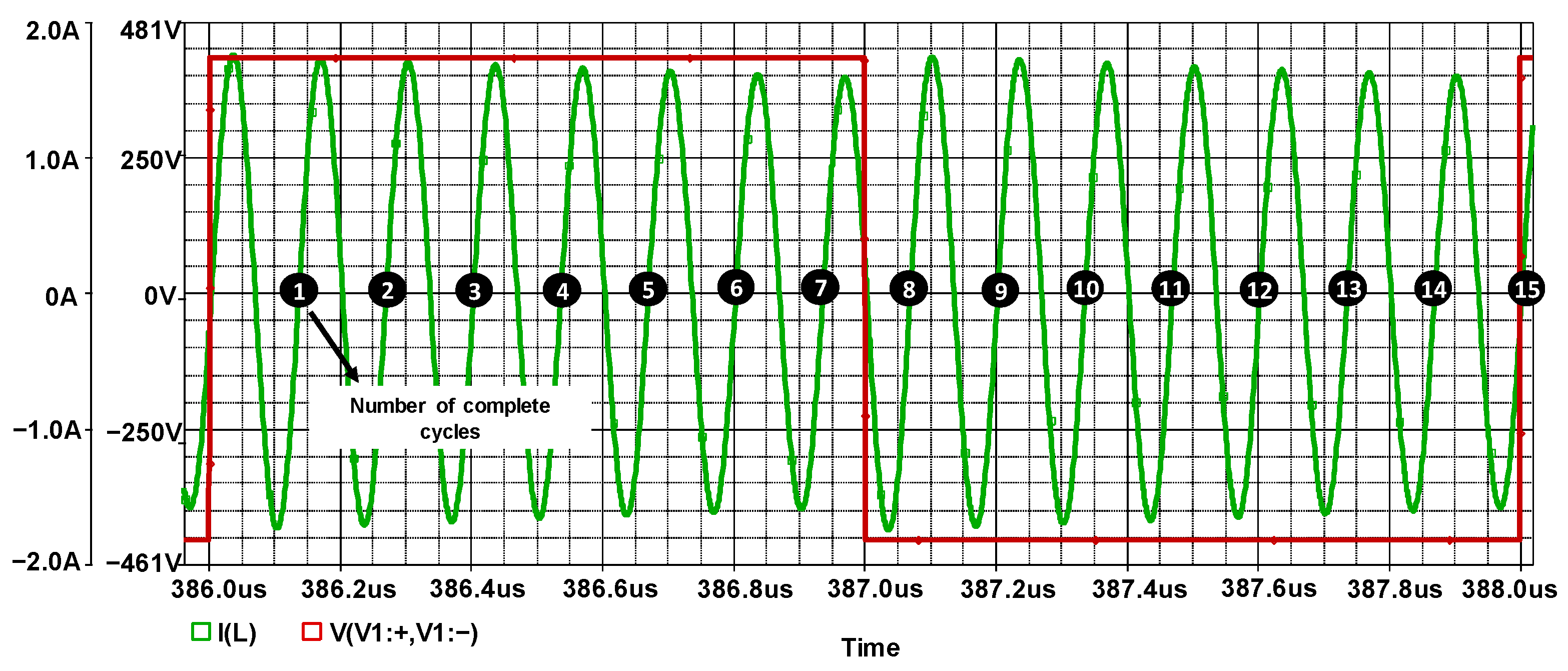
Current in the resonant tank (sinusoidal waveform) with “n” complete cycles in one cycle of the bipolar voltage source (square waveform).
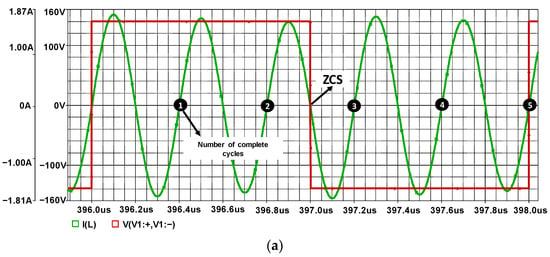
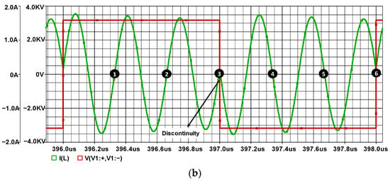
Figure 14.
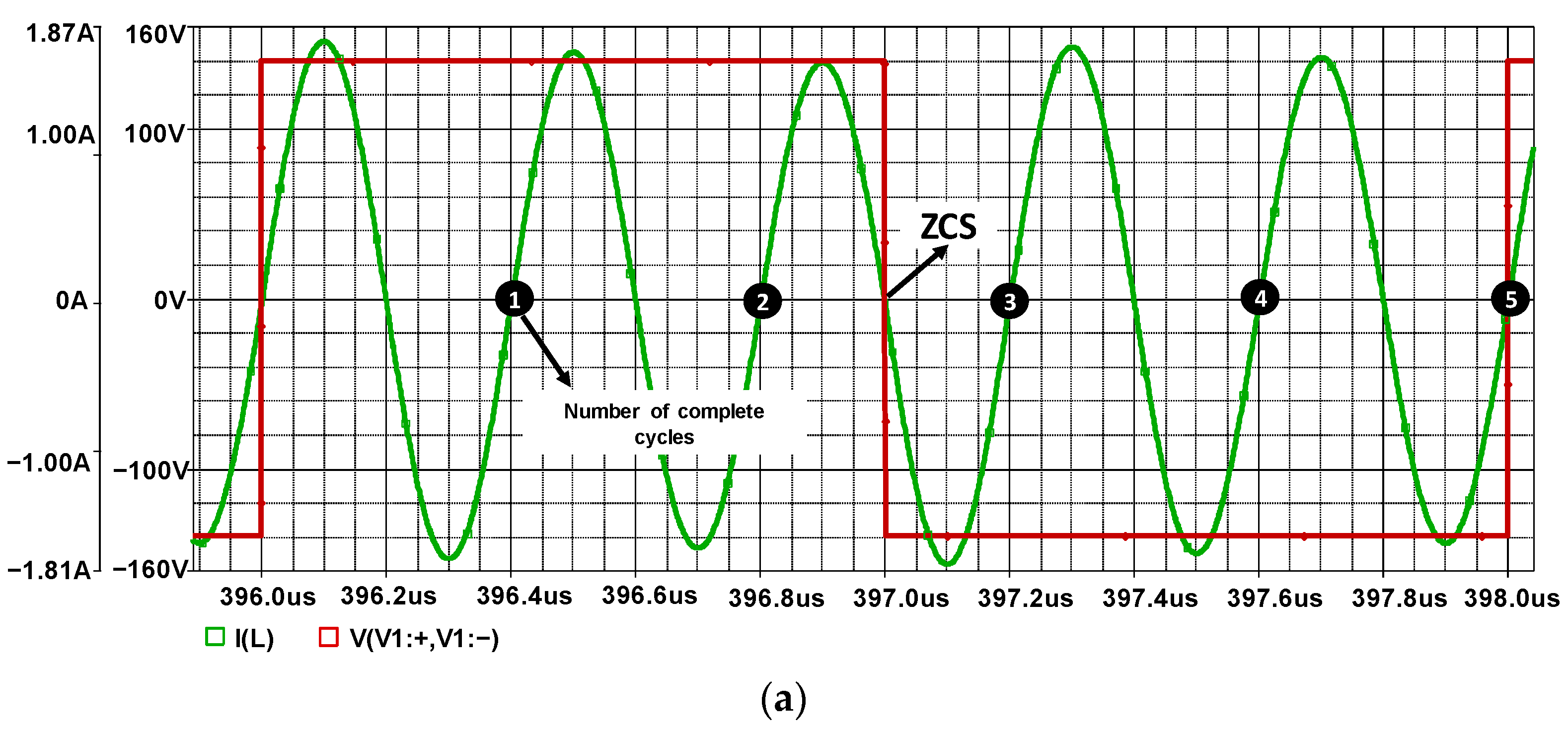
Current in the resonant tank (sinusoidal waveform) with different values of “n”. (a) Current in the resonant tank with an odd value of “n = 5” and ZCS. (b) Current in the resonant tank with an even value of “n = 6”.
As shown in Figure 9 and Figure 10, the values of the RMS voltage and the average power obtained in the simulation are the same as the proposed values in Table 1 (Vout = 25 V, Po = 30 W). Figure 11 shows the current in the resonant tank oscillating at the proposed frequency of 7.5 MHz (fo = fswn) with the calculated peak current value of 1.72 A. Figure 12 shows the voltage level in the resonant capacitor in the middle of the switching period, which is equal to the DC voltage multiplied by the value of the constant “codd” (VC = coddVDC). Figure 13 shows the current in the resonant tank (sinusoidal waveform) and the voltage applied at the input of the circuit (square waveform). As can be seen in Figure 13, the frequency of the current in the resonant tank is multiplied fifteen times “n = 15” the switching frequency of the square bipolar voltage source. Furthermore, the current waveform shows that the maximum value of the current is decaying with a damping factor of “df = 0.9” (almost sinusoidal) as defined in Table 1. The results shown in Figure 9, Figure 10, Figure 11, Figure 12, Figure 13 and Figure 14 demonstrate that the methodology for operating the RLC circuit in a transient state, acting as a frequency multiplier, was correctly designed since they are very close to the theoretical values shown in Table 1 and Table 2.
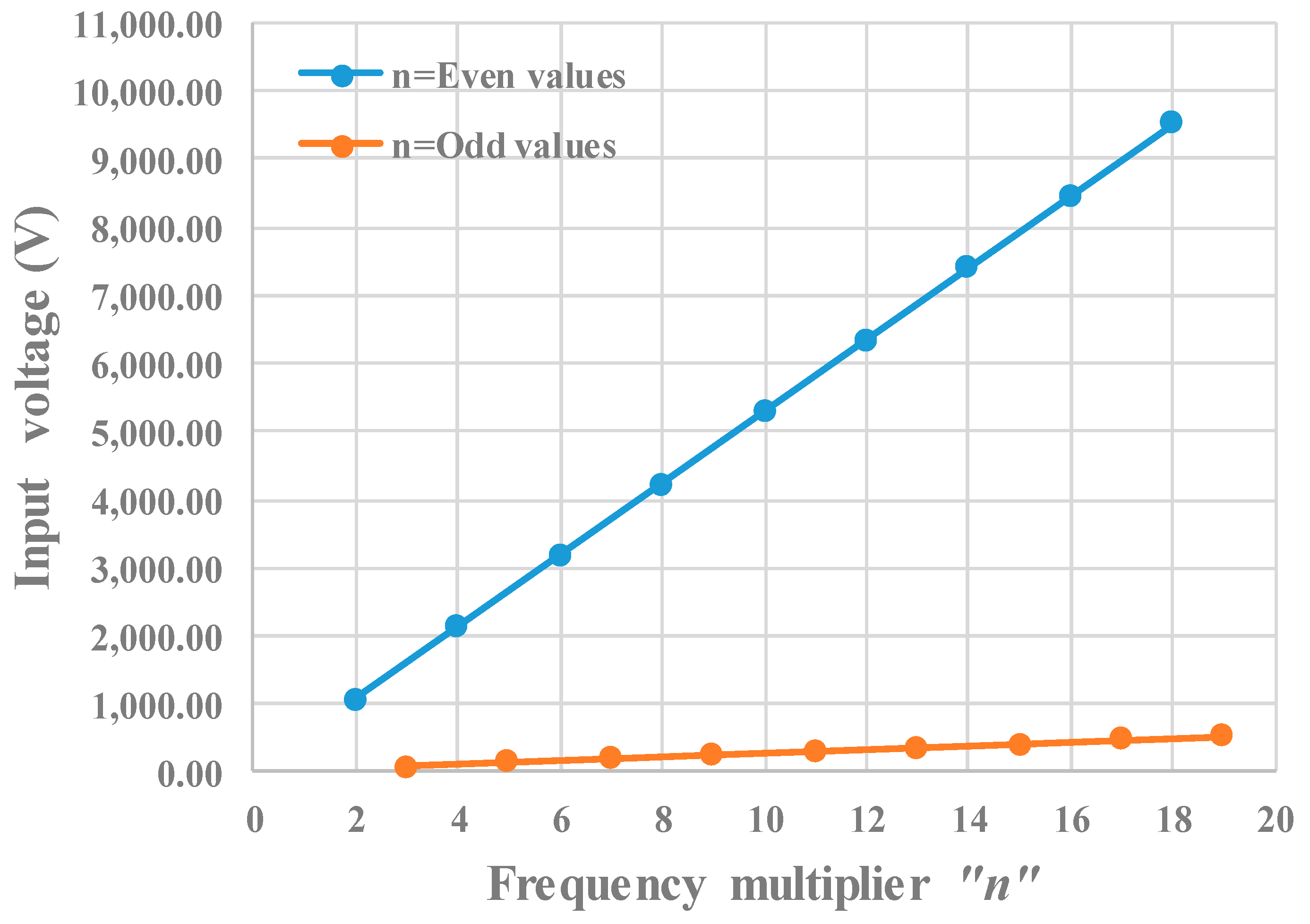
More simulations were performed with even and odd values of “n”, following the design methodology proposed in Table 2, with the same output power (Po = 30 W) to show the difference in the current waveform. Figure 14a shows the resonant current with n = 5 (odd value); this figure shows the continuity of the current throughout the square voltage switching period, while Figure 14b shows the resonant current with n = 6 (even value). In this case, a discontinuity is observed in the middle of the square voltage switching period (D = 50%). Figure 14a also demonstrates that even though the series RLC resonant circuit was designed in a transient state, it is presenting zero current switching (ZCS), similar to the resonant circuits designed in a steady state. This characteristic allows the possibility of using this design methodology for the design of high-frequency resonant converters. The difference between using even or odd values of “n” is very important in the operation of the circuit since, as can be seen in both figures, when using even values of “n”, the input supply voltage (VDC = 3.1 kV) required is much higher than the required voltage when using odd values of “n” (VDC = 140 V). Figure 15 shows graphically the difference between the input supply voltages (VDC) for each case using the same output power (Po = 30 W) and the same square voltage source switching frequency (500 kHz). With even values of “n”, the necessary input voltage reaches voltages of almost 10 kV; with odd values of “n”, the necessary input voltage is lower than 600 V. The difference in the supply voltage level is due to the value of the constants ceven or codd. When using even values of the multiplier “n”, small values of the constant ceven are obtained; therefore, a large supply voltage level is necessary because the voltage stored in the capacitor is not sufficient to obtain the frequency multiplication and underdamping. The opposite is true when using odd values in the multiplier “n”, where the value of the constant codd is higher and a very large supply voltage is not necessary. The effect of the value of the constants ceven or codd can also be observed in the gain of the circuit, as shown in Figure 6 and Figure 7. Due to the higher increase of the input supply voltage by increasing the multiplier “n”, there are increases in the instantaneous input power that the power supply must be able to supply. To compare the electrical power demanded from the power supply using odd or even values in the multiplier “n”, a term called power demand rate “Pd” is introduced, which is calculated as follows:
where Pmax represents the maximum peak power demanded from the power source and Pavg represents the average output power at the load resistor.
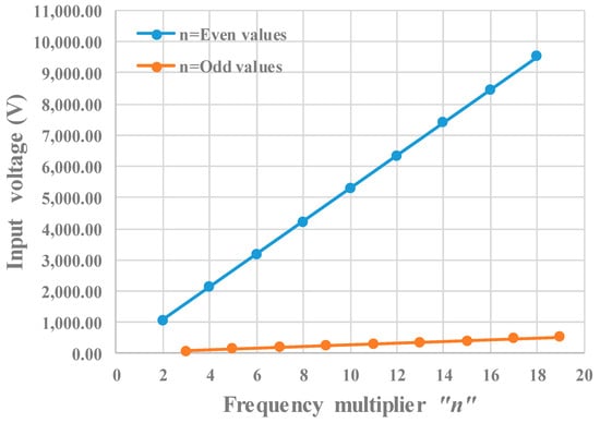
Figure 15.
Input supply voltage (VDC) required for different values of the frequency multiplier “n” with the same output power (Po = 30 W).
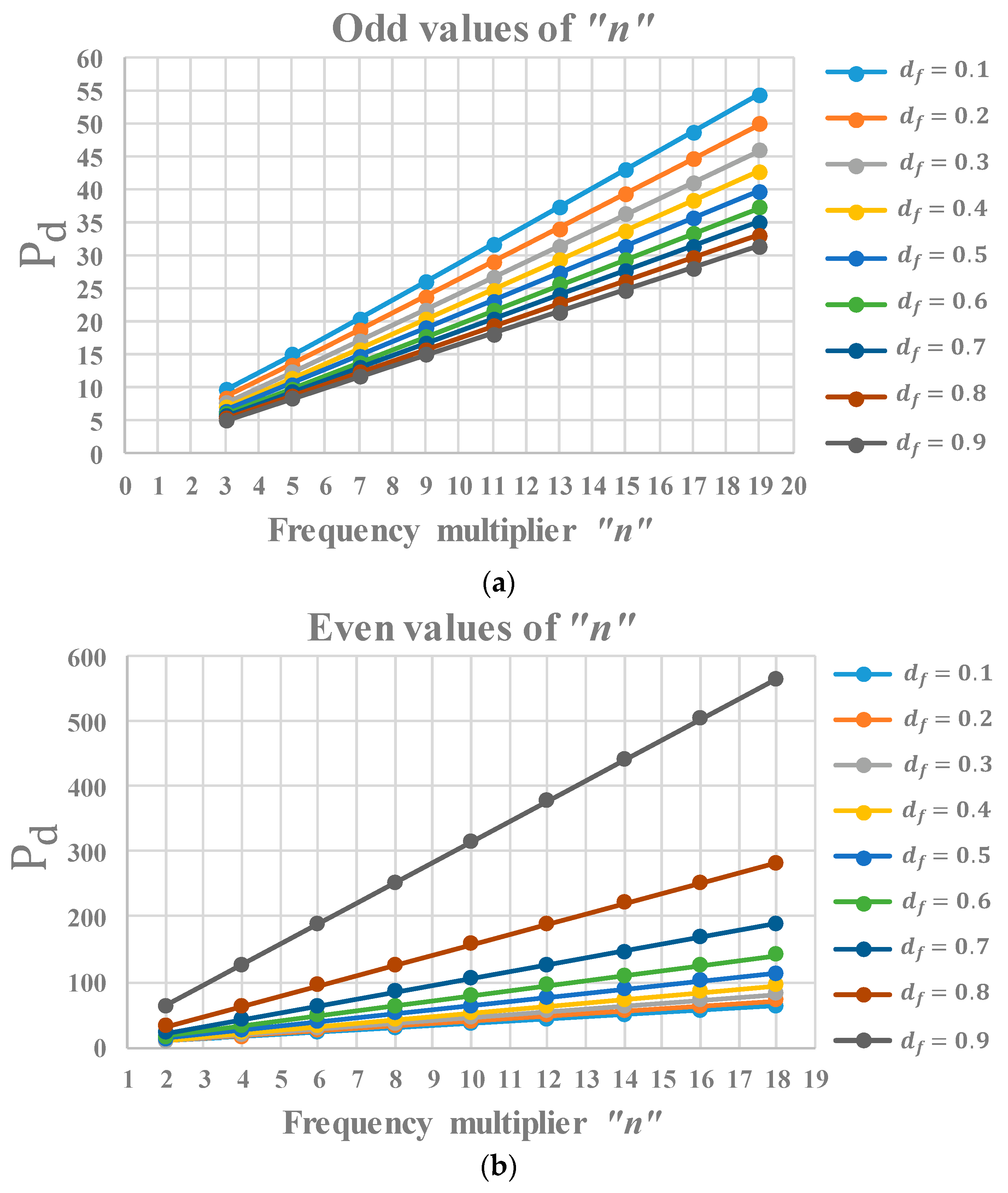
To appreciate the effect that the multiplier “n” has on the power demand of the circuit, Figure 16 shows the rate of power demanded when varying the multiplier “n” in odd and even values, with the output power of 30 watts for both cases. As shown in Figure 16a, there is a lower power demand rate to the power supply when using odd values of “n compared to using even values of “n”, where the power demand is multiplied up to almost ten times, as shown in Figure 16b. Although lower power levels are demanded when using odd values of “n”, the power level is much higher than those demanded by resonant circuits designed in a steady state. This should be considered in the design of transient state resonant circuits for certain applications.
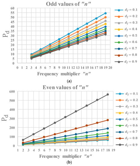
Figure 16.
Power demand rate (Pd) from the power supply for different values of the frequency multiplier “n”, same output power (Po = 30 W), and fixed damping factor “df”. (a) Power demand rate (Pd) for odd values of “n”. (b) Power demand rate (Pd) for even values of “n”.
As shown in Figure 9, Figure 10, Figure 11, Figure 12, Figure 13 and Figure 14, it was possible to obtain a frequency multiplication in the tank up to fifteen times. This transient state design methodology achieves resonant frequency multiplication by manipulating the values of the passive components in the resonant tank to operate the circuit in an underdamped mode. The reported papers where the VFX frequency multiplication technique had been used only achieved a frequency multiplication of the double, which was established in their design by manipulating the frequency of the inverter/rectifier stage using control methods [22,23,24,25]. Furthermore, those reported in [20,21], where class E/DE amplifiers had been used without using control methods in the inverter stage, achieved a frequency multiplication of up to three times.
The analysis shown in this paper, including the design of resonant circuits in a transient state with underdamped response, theoretically allows a frequency multiplication much higher than those reported in the literature and does not require sophisticated electronic devices or complex control methods. However, applying this design methodology has some disadvantages, since, as shown in Figure 4, to achieve a high-frequency multiplication (n > 15), it is necessary to have high levels of quality factor in the resonant tank. Therefore, the practical implementation with n > 15 might cause important losses in the passive elements and in the parasitic of the switches used in the inverter. Figure 16a shows that for n < 10, the power demand rate is under 30 (Pd < 30) for odd values of n. Therefore, the practical implementation in this range will be more feasible. These considerations should be considered when applying this design methodology in experimental tests, where no special electronic components are required. As shown in Figure 1, the bipolar voltage source at the input of the circuit can be replaced by the output voltage of a full-bridge inverter, allowing the possibility of implementing this transient analysis in the design of resonant converters for applications where very high operating frequencies are required.
4. Conclusions
This paper presented the transient state analysis and design methodology of a series RLC circuit which multiplied the oscillation frequency of the current in the resonant tank “n” number of times the switching frequency of the square bipolar voltage source “fsw”. The design methodology proposed in Table 2 was verified by simulations in OrCAD PSpice, where the design parameters of the circuit shown in Table 1 could be achieved since it was possible to multiply the oscillation frequency of the current “n = 15” times in the resonant tank and deliver the required power level to the load (Po = 30 W). It was determined that the gain of the series RLC circuit with underdamped response changes depending on whether the values of “n” are even or odd and depending on the damping factor “df”, where the gain using odd values of “n” does not present large variations when using different values of the damping factor “df”, as shown in Figure 7. Another disadvantage of using even values of the multiplier “n” is that the current presents a discontinuity in the middle of the square voltage switching period, as shown in Figure 14b. In addition, another difference is the voltage level required and the maximum instantaneous power demanded from the power supply since, as shown in Figure 15, using even values of “n” meant higher supply voltage levels were needed to transmit the same power level to the load. Furthermore, as shown in Figure 16b, almost ten times more maximum power level was demanded from the power supply when using even values of “n”. These results show that using odd values of “n” is more convenient since lower instantaneous power peaks are demanded from the source, lower voltage levels are necessary, the gain presents minor variations when using different damping factors “df”, and the current waveform is sinusoidal without discontinuities. The design methodology and analysis shown in this paper demonstrates that it is possible to multiply the frequency without using complex control methods, such as VFX, which only varies the frequency of the inverter/rectifier to obtain certain gains. In this method, the switching frequency remains constant, and it is the resonance frequency that is multiplied, allowing the design of very high-frequency resonant converters with low-level inverter switching frequencies.
Author Contributions
Conceptualization, J.L.-R., M.P.-S. and S.E.D.-A.; data curation, J.L.-R., M.P.-S. and C.C.-G.; formal analysis, J.L.-R., M.P.-S., L.H.-G. and C.C.-G.; funding acquisition, M.P.-S., L.H.-G. and J.R.-H.; investigation, J.L.-R., M.P.-S. and S.E.D.-A.; methodology, M.P.-S., S.E.D.-A. and C.C.-G.; project administration, L.H.-G. and J.R.-H.; resources, J.R.-H. and M.P.-S.; software, J.L.-R. and M.P.-S.; supervision, M.P.-S. and C.C.-G.; validation, J.L.-R., M.P.-S. and L.H.-G.; visualization, J.L.-R. and J.R.-H.; writing—original draft, J.L.-R., M.P.-S. and C.C.-G.; writing—review & editing, L.H.-G., J.R.-H. and S.E.D.-A. All authors have read and agreed to the published version of the manuscript.
Funding
This work was funding by Instituto Politécnico Nacional and Tecnológico Nacional de México-CENIDET.
Conflicts of Interest
The authors declare no conflict of interest.
References
- Kshatri, S.S.; Dhillon, J.; Mishra, S.; Haghighi, A.T.; Hunt, J.D.; Patro, E.R. Comparative Reliability Assessment of Hybrid Si/SiC and Conventional Si Power Module Based PV Inverter Considering Mission Profile of India and Denmark Locations. Energies 2022, 15, 8612. [Google Scholar] [CrossRef]
- Alatai, S.; Salem, M.; Ishak, D.; Das, H.S.; Nazari, M.A.; Bughneda, A.; Kamarol, M. A Review on State-of-the-Art Power Converters: Bidirectional, Resonant, Multilevel Converters and Their Derivatives. Appl. Sci. 2021, 11, 10172. [Google Scholar] [CrossRef]
- İnci, M.; Büyük, M.; Demir, M.H.; İlbey, G. A review and research on fuel cell electric vehicles: Topologies, power electronic converters, energy management methods, technical challenges, marketing and future aspects. Renew. Sustain. Energy Rev. 2021, 137, 110648. [Google Scholar] [CrossRef]
- Chen, C.; Chen, Y.; Tan, Y.; Fang, J.; Luo, F.; Kang, Y. On the practical design of a high power density SiC single-phase uninterrupted power supply system. IEEE Trans. Ind. Inform. 2017, 13, 2704–2716. [Google Scholar] [CrossRef]
- Mahesh, M.; Kumar, K.V.; Abebe, M.; Udayakumar, L.; Mathankumar, M. A review on enabling technologies for high power density power electronic applications. Mater. Today Proc. 2021, 46, 3888–3892. [Google Scholar] [CrossRef]
- Baek, J.; Park, M.-H.; Kim, T.; Youn, H.-S. Modified power factor correction (PFC) control and printed circuit board (PCB) design for high-efficiency and high-power density on-board charger. Energies 2021, 14, 605. [Google Scholar] [CrossRef]
- Kwon, J.; Kim, R.-Y. High power density, high-voltage parallel resonant converter using parasitic capacitance on the secondary side of a transformer. Electronics 2021, 10, 1736. [Google Scholar] [CrossRef]
- Gu, L.; Zulauf, G.; Stein, A.; Kyaw, A.; Chen, T.; Davila, J.M.R. 6.78-MHz wireless power transfer with self-resonant coils at 95% DC–DC efficiency. IEEE Trans. Power Electron. 2020, 36, 2456–2460. [Google Scholar] [CrossRef]
- Shi, L.; Alou, P.; Oliver, J.A.; Cobos, J.A. A Novel Self-adaptive Wireless Power Transfer System to Cancel the Reactance of the Series Resonant Tank and Deliver More Power. In Proceedings of the 2019 IEEE Energy Conversion Congress and Exposition (ECCE), Baltimore, MD, USA, 29 September–3 October 2019; pp. 4207–4211. [Google Scholar]
- Yoo, J.-S.; Gil, Y.-M.; Ahn, T.-Y. Steady-State Analysis and Optimal Design of an LLC Resonant Converter Considering Internal Loss Resistance. Energies 2022, 15, 8144. [Google Scholar] [CrossRef]
- Stojadinovic, N.; Dankovic, D.; Manic, I.; Davidovic, V.; Djoric-Veljkovic, S.; Golubovic, S. Impact of negative bias temperature instabilities on lifetime in p-channel power VDMOSFETs. In Proceedings of the 8th IEEE International Conference on Telecommunications in Modern Satellite, Cable and Broadcasting Services, Nis, Serbia, 26–28 September 2007; pp. 275–282. [Google Scholar]
- Djezzar, B.; Tahi, H.; Benabdelmoumene, A.; Chenouf, A. A new eye on NBTI-induced traps up to device lifetime using on the fly oxide trap method. In Proceedings of the 24th IEEE International Conference on Microelectronics (ICM), Algiers, Algeria, 16–20 December 2012; pp. 1–4. [Google Scholar]
- Tahi, H.; Tahanout, C.; Boubaaya, M.; Djezzar, B.; Merah, S.M.; Nadji, B.; Saoula, N. Experimental investigation of NBTI degradation in power VDMOS transistors under low magnetic field. IEEE Trans. Device Mater. Reliab. 2017, 17, 99–105. [Google Scholar] [CrossRef]
- Stojadinović, N.; Djorić-Veljković, S.; Davidović, V.; Golubović, S.; Stanković, S.; Prijić, A.; Prijić, Z.; Manić, I.; Danković, D. NBTI and irradiation related degradation mechanisms in power VDMOS transistors. Microelectron. Reliab. 2018, 88, 135–141. [Google Scholar] [CrossRef]
- Park, H.-P.; Kang, Y.; Kang, S.; Jung, J.-H. FPGA Controller Design for High-Frequency LLC Resonant Converters. IEEJ J. Ind. Appl. 2020, 9, 523–529. [Google Scholar] [CrossRef]
- Zhao, Y.; Xiao, Q.; Zhang, Z.; Zhao, X.; Lin, D. Research on ZVS Phase-Shifted Full-Bridge Broadband Inverter Based on Auxiliary Current Source. Energies 2022, 15, 8661. [Google Scholar] [CrossRef]
- Xu, S.; Wang, Z.; Chen, J.; Jiang, W. Research and Design of LC Series Resonant Wireless Power Transfer System with Modulation Control Method for Supercapacitor Charging in Linear Motion Systems. Energies 2022, 15, 6739. [Google Scholar] [CrossRef]
- Huang, J.; Wong, S.-C.; Liu, X.; Li, Z. Steady State Analysis of Wireless Power Transfer System with Rectifier-Load under DCM. In Proceedings of the 14th IEEE Conference on Industrial Electronics and Applications, Xi’an, China, 19–21 June 2019; pp. 462–467. [Google Scholar]
- Li, X.; Guo, L.; Lang, T.; Lu, D.; Alluhaybi, K.; Hu, H. Steady-State Characterization of LLC-Based Single-Stage AC/DC Converter Based on Numerical Analysis. IEEE Trans. Power Electron. 2021, 36, 9970–9983. [Google Scholar] [CrossRef]
- Shinoda, K.; Fujii, M.; Matsuo, M.; Suetsuga, T.; Mori, S. Idealized operation of Class DE frequency multipliers. In Proceedings of the IEEE International Symposium on Circuits and Systems (ISCAS), Atlanta, GA, USA, 15 May 1996; Volume 1, pp. 581–584. [Google Scholar]
- Zulinski, R.; Steadman, J. Idealized operation of class E frequency multipliers. IEEE Trans. Circuits Syst. 1986, 33, 1209–1218. [Google Scholar] [CrossRef]
- Inam, W.; Afridi, K.K.; Perreault, D.J. Variable frequency multiplier technique for high-efficiency conversion over a wide operating range. IEEE J. Emerg. Sel. Top. Power Electron. 2015, 4, 335–343. [Google Scholar] [CrossRef]
- Li, R.T.; Vancu, M.-F.; Canales, F.; Aggeler, D. High performance dc-dc converter for wide voltage range operation. In Proceedings of the 7th International Power Electronics and Motion Control Conference, Harbin, China, 2–5 June 2012; Volume 2, pp. 1151–1158. [Google Scholar]
- Shinoda, K.; Fujii, M.; Koizumi, H.; Suetsugu, T.; Mori, S. Phase-controlled resonant dc/dc converter with Class E frequency multiplier. In Proceedings of INTELEC 95. In Proceedings of the 17th International Telecommunications Energy Conference, The Hague, The Netherlands, 29 October–1 November 1995; pp. 107–113. [Google Scholar]
- Gu, L.; Liang, W.; Praglin, M.; Chakraborty, S.; Rivas-Davila, J. A wide-input-range high-efficiency step-down power factor correction converter using a variable frequency multiplier technique. IEEE Trans. Power Electron. 2018, 33, 9399–9411. [Google Scholar] [CrossRef]
- Li, Y.; Meng, J.; Zhang, D.; Zhu, H. The Development of Frequency Tripler Based on Six-Anode Schottky Varactors. Micromachines 2021, 12, 1490. [Google Scholar] [CrossRef]
- Oh, K.-I.; Ko, G.-H.; Kim, G.-S.; Kim, J.-G.; Baek, D. A 17.8–34.8 GHz (64.6%) Locking Range Current-Reuse Injection-Locked Frequency Multiplier with Dual Injection Technique. Electronics 2021, 10, 1122. [Google Scholar] [CrossRef]
- Powell, J.; Viegas, C.; Sanghera, H.S.; Huggard, P.G.; Alderman, B. Comparing novel MMIC and hybrid circuit high efficiency GaAs Schottky diode mm-wave frequency doublers. Electronics 2020, 9, 1718. [Google Scholar] [CrossRef]
- Doo, J.; Kim, J.; Jeong, J. D-band frequency tripler module using anti-parallel diode pair and waveguide transitions. Electronics 2020, 9, 1201. [Google Scholar] [CrossRef]
- Jeong, J.; Choi, J.; Kim, J.; Choe, W. H-band INP HBT frequency tripler using the triple-push technique. Electronics 2020, 9, 2081. [Google Scholar] [CrossRef]
- Yao, J.; Li, M.; Yu, X.; Li, T.; Dai, Z. Analysis and Design of Class E Frequency Multiplier With Shunt Linear and Nonlinear Capacitances at Any Duty Cycle. IEEE Trans. Circuits Syst. II Express Briefs 2021, 69, 1827–1831. [Google Scholar] [CrossRef]
- Zaheri, R.; Moghani, J.S. A Modular Two-Stage High Step-Down DC-DC Converter Using Frequency Multiplier Circuit for Datacenter Applications. In Proceedings of the IEEE 12th Power Electronics, Drive Systems, and Technologies Conference (PEDSTC), Tabriz, Iran, 2–4 February 2021; pp. 1–5. [Google Scholar]
- Jia, P.; Guo, H.; Yuan, G.; Zhu, H.; Su, Z.; Guo, T. Prediction for the Overcurrent Value of the Three-Level LLC Resonant Converter in the Mode Switching Process. In Proceedings of the IEEE 24th International Conference on Electrical Machines and Systems (ICEMS), Gyeongju, Korea, 31 October–3 November 2021; pp. 211–2115. [Google Scholar]
- Sumi, F.H.; Dutta, L.; Sarker, F. Future with Wireless power transfer technology. J. Electr. Electron. Syst. 2018, 7, 1000279. [Google Scholar]
- Feng, J.; Li, Q.; Lee, F.C.; Fu, M. LCCL-LC Resonant Converter and Its Soft Switching Realization for Omnidirectional Wireless Power Transfer Systems. IEEE Trans. Power Electron. 2020, 36, 3828–3839. [Google Scholar] [CrossRef]
- Pahlavan, S.; Shooshtari, M.; Ashtiani, S.J. Star-Shaped Coils in the Transmitter Array for Receiver Rotation Tolerance in Free-Moving Wireless Power Transfer Applications. Energies 2022, 15, 8643. [Google Scholar] [CrossRef]
- Aydin, E.; Aydemir, M.T.; Aksoz, A.; el Baghdadi, M.; Hegazy, O. Inductive Power Transfer for Electric Vehicle Charging Applications: A Comprehensive Review. Energies 2022, 15, 4962. [Google Scholar] [CrossRef]
- Jha, R.K.; Kumar, A.; Prakash, S.; Jaiswal, S.; Bertoluzzo, M.; Kumar, A.; Joshi, B.P.; Forato, M. Modeling of the Resonant Inverter for Wireless Power Transfer Systems Using the Novel MVLT Method. Vehicles 2022, 4, 1277–1287. [Google Scholar] [CrossRef]
- Erickson, R.W.; Maksimovic, D. Fundamentals of Power Electronics; Springer Science & Business Media: Berlin/Heidelberg, Germany, 2007. [Google Scholar]
- Robinson, J.C. An Introduction to Ordinary Differential Equations; Cambridge University Press: Cambridge, UK, 2004. [Google Scholar]
Publisher’s Note: MDPI stays neutral with regard to jurisdictional claims in published maps and institutional affiliations. |
© 2022 by the authors. Licensee MDPI, Basel, Switzerland. This article is an open access article distributed under the terms and conditions of the Creative Commons Attribution (CC BY) license (https://creativecommons.org/licenses/by/4.0/).

