
Design and Analysis of a DC Solid-State Circuit Breaker for Residential Energy Router Application


Abstract
:1. Introduction
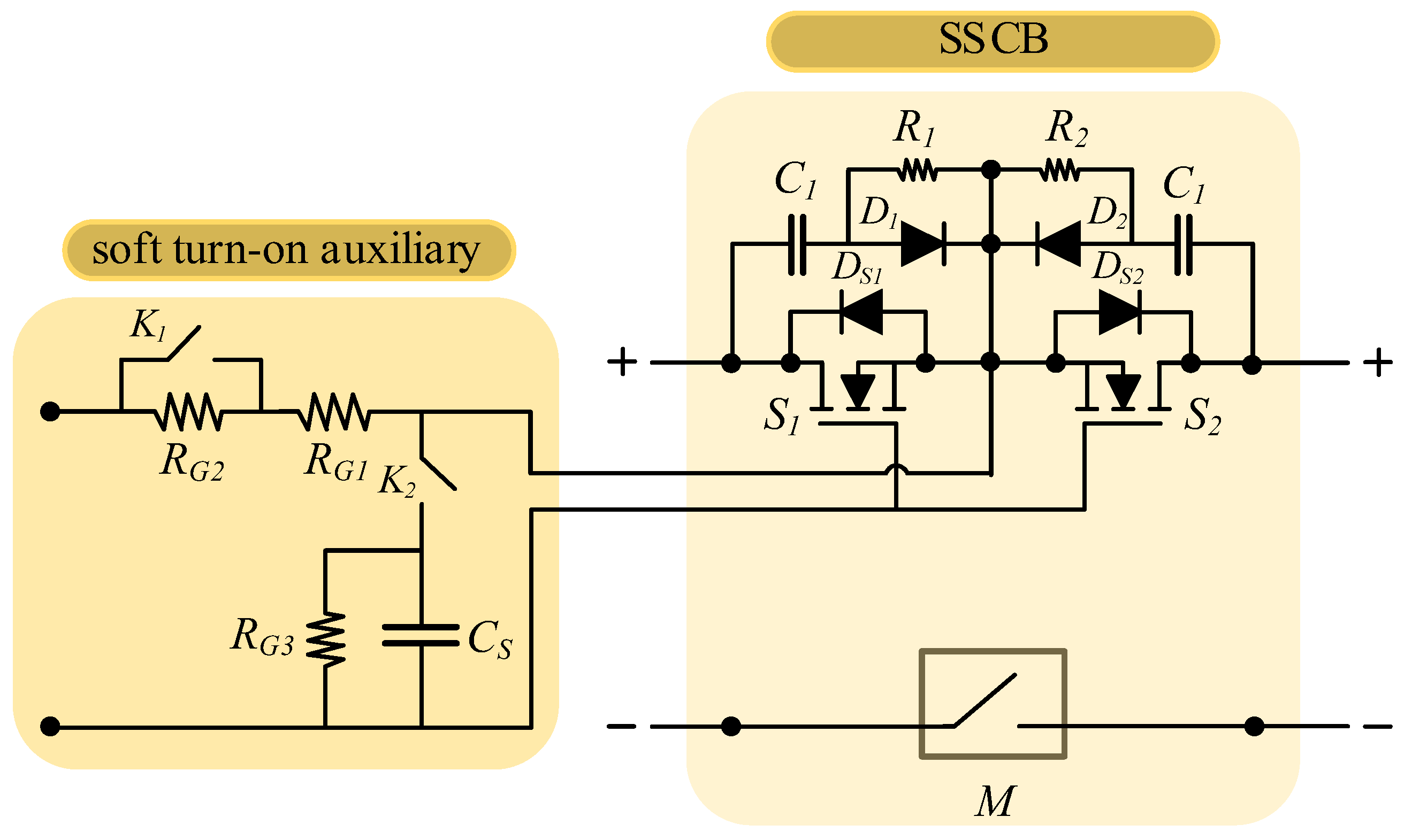
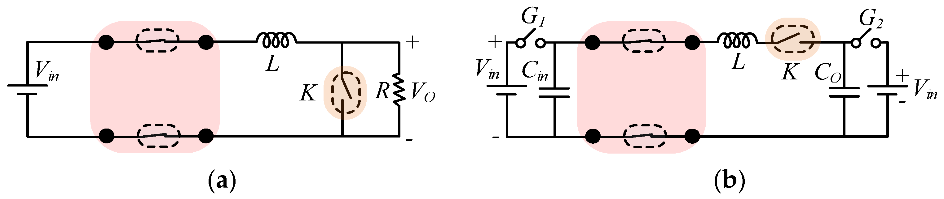
2. Investigation of the Topology
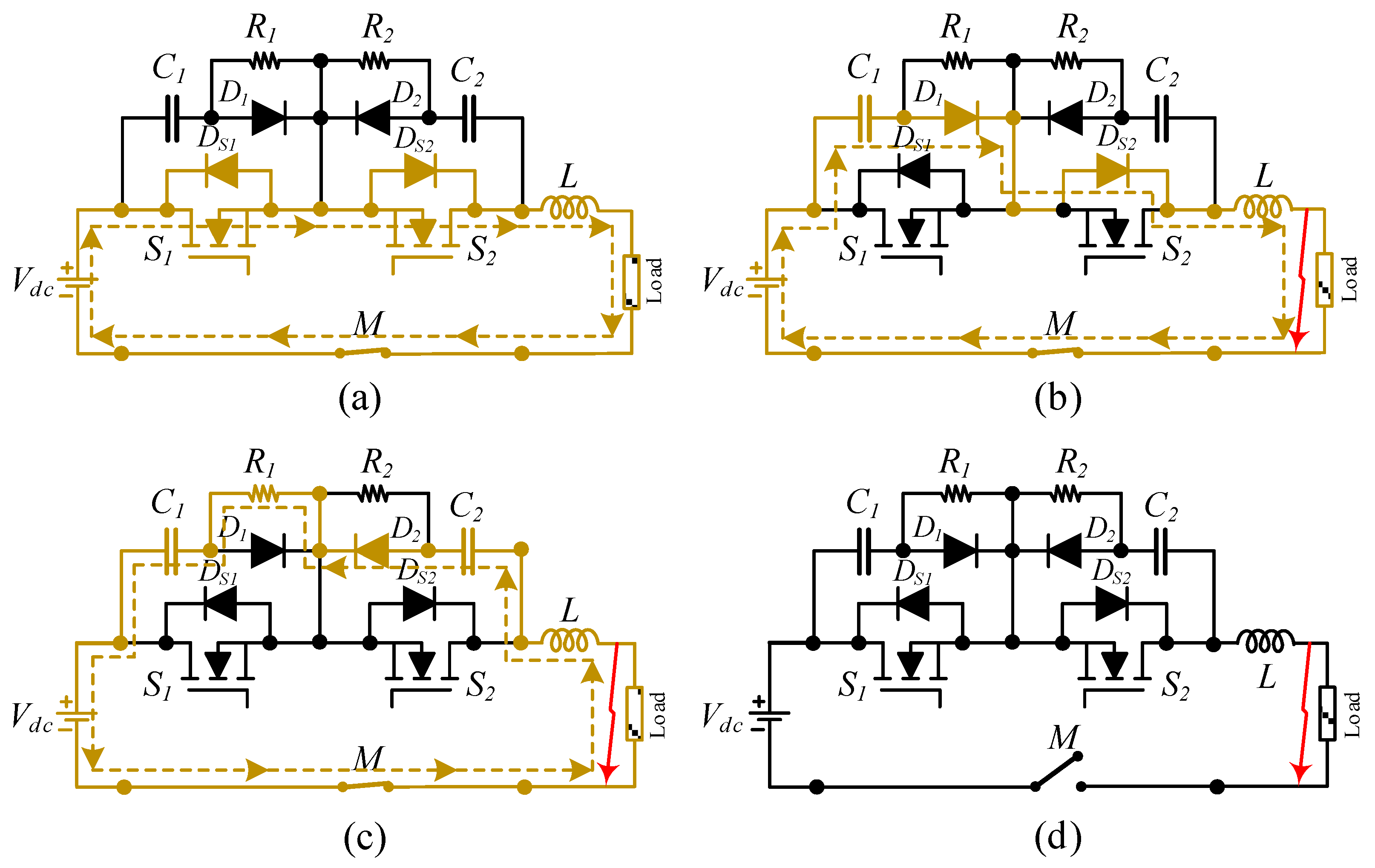
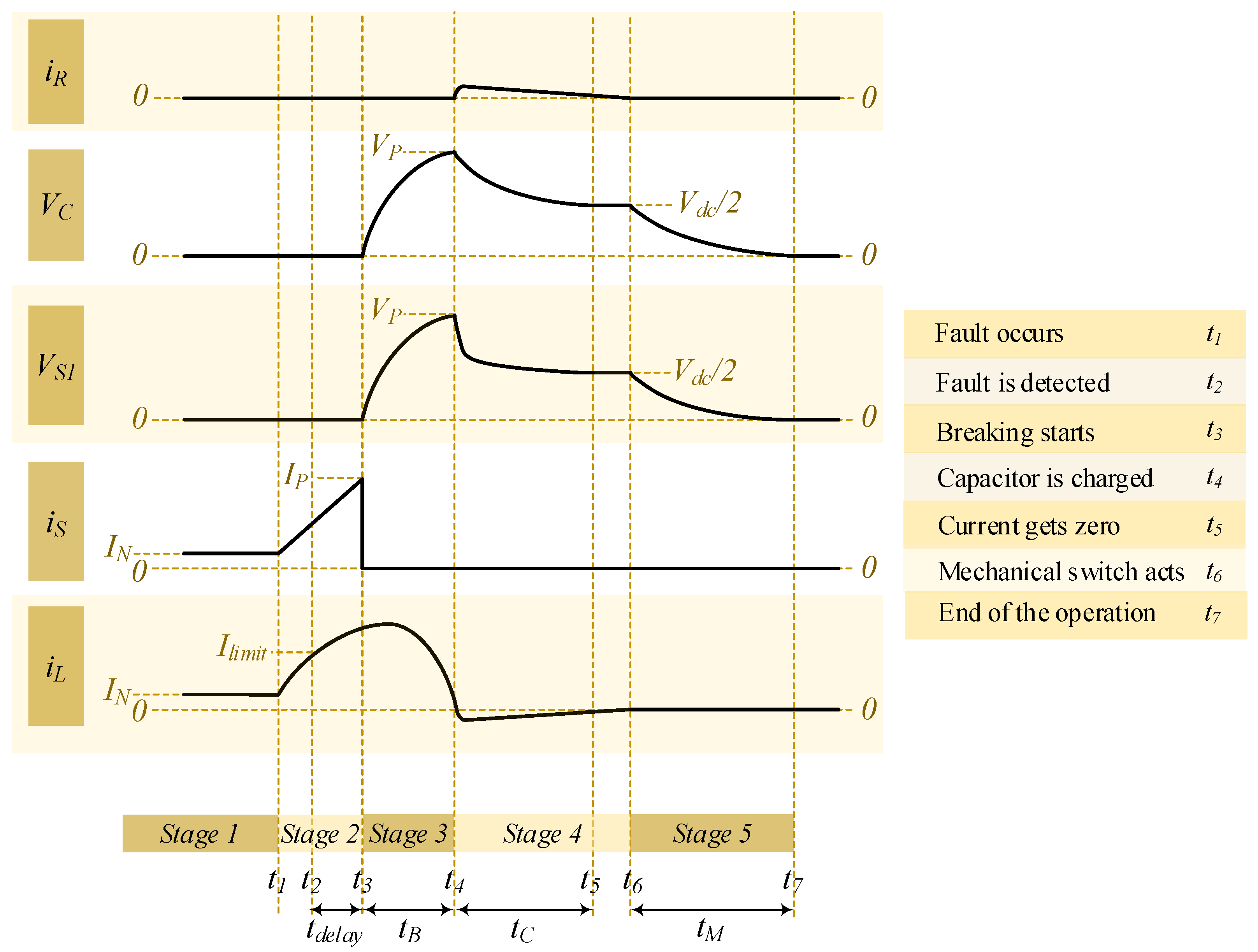
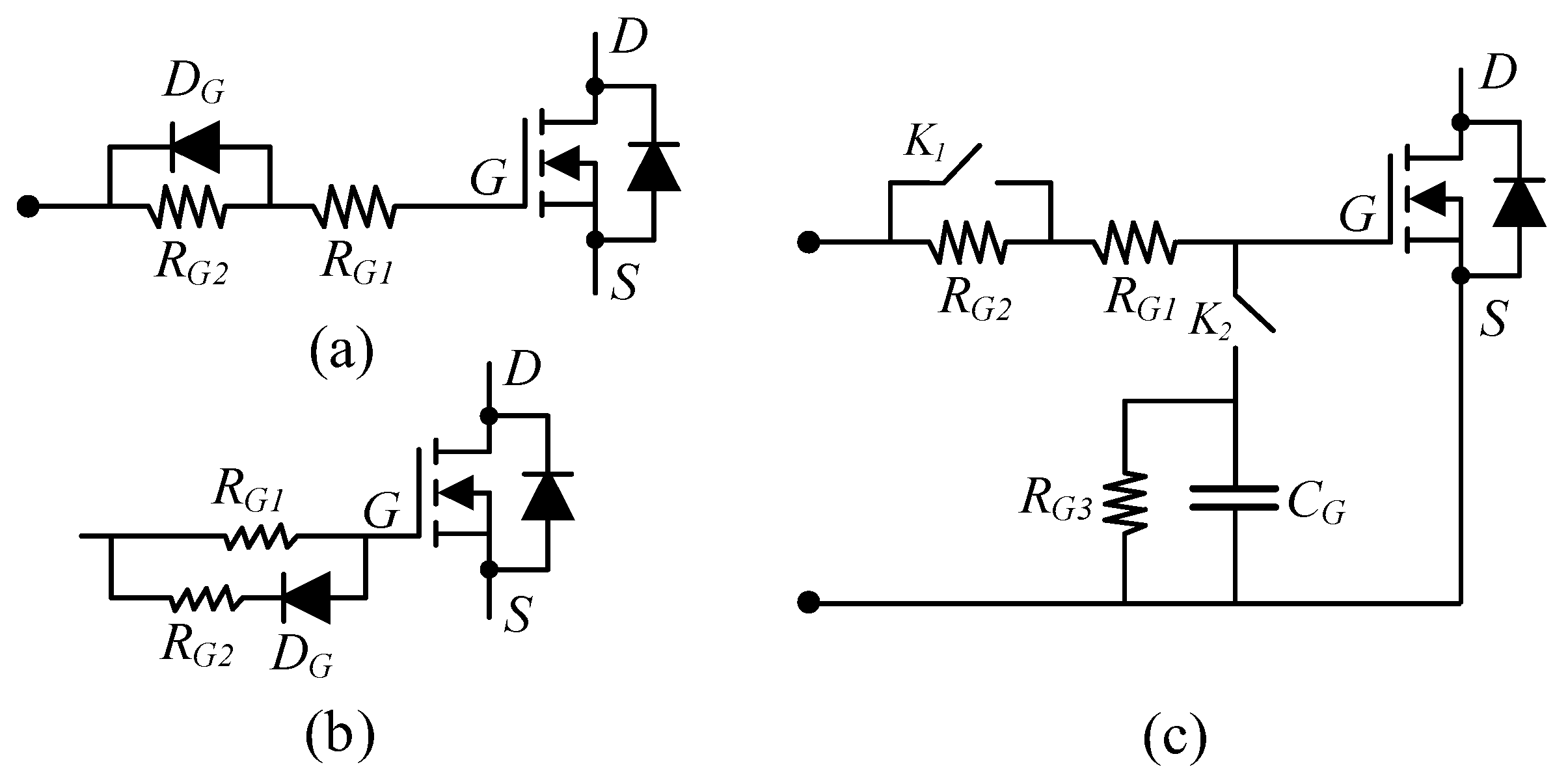
2.1. Stage 1
2.2. Stage 2
2.3. Stage 3
2.4. Stage 4
2.5. Stage 5
3. Design Procedure
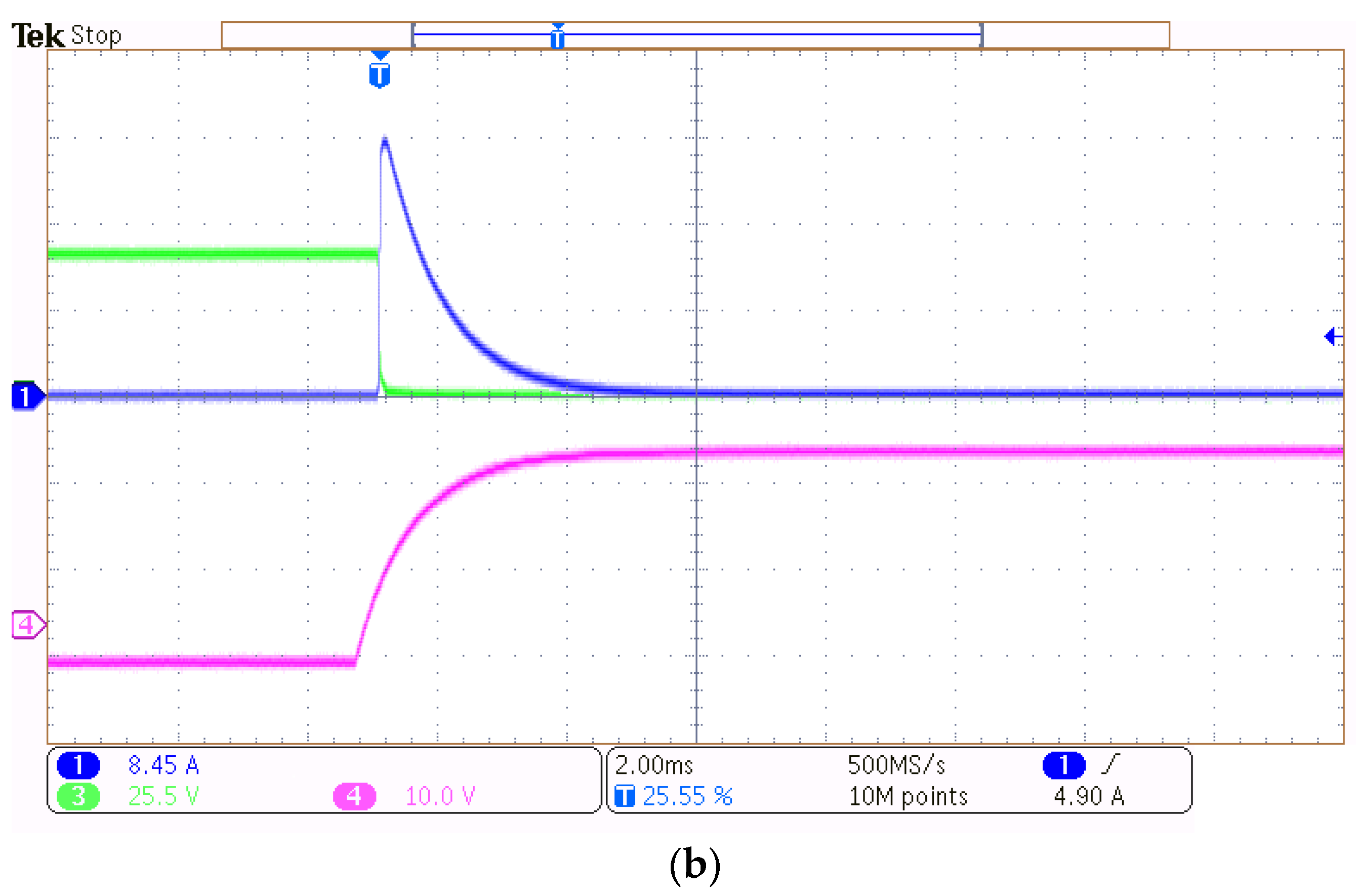
3.1. Short-Circuit Fault Operation
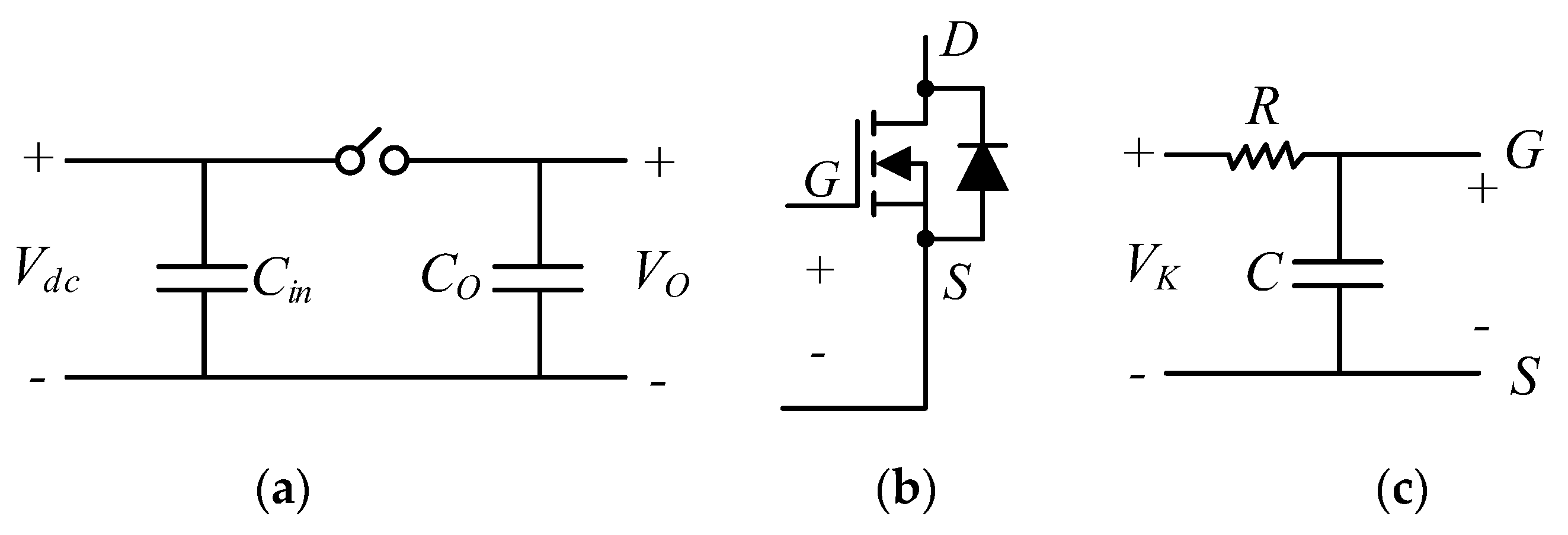
3.2. Soft Turn-On Operation
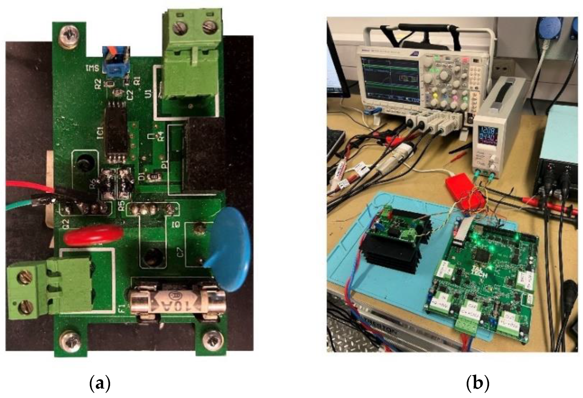
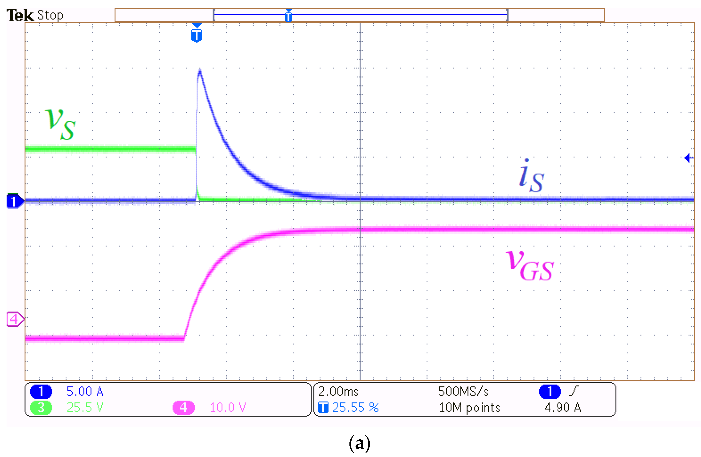
4. Experimental Results
5. Conclusions
Author Contributions
Funding
Data Availability Statement
Conflicts of Interest
References
- Wang, R.; Jiang, S.; Ma, D.; Sun, Q.; Zhang, H.; Wang, P. The Energy Management of Multi-port Energy Router in Smart Home. IEEE Trans. Consum. Electron. 2022, 68, 344–353. [Google Scholar] [CrossRef]
- Roasto, I.; Husev, O.; Najafzadeh, M.; Jalakas, T.; Rodriguez, J. Voltage source operation of the energy-router based on model predictive control. Energies 2019, 12, 1892. [Google Scholar] [CrossRef] [Green Version]
- Wang, K.; Hu, X.; Li, H.; Li, P.; Zeng, D.; Guo, S. A Survey on Energy Internet Communications for Sustainability. IEEE Trans. Sustain. Comput. 2017, 2, 231–254. [Google Scholar] [CrossRef]
- Chen, M.; Xia, M.; Chen, Q. A two-stage planning method of the energy router considering the optimal operation in distribution network. CSEE J. Power Energy Syst. 2022, 1–13. [Google Scholar] [CrossRef]
- Liang, H.; Hua, H.; Qin, Y.; Ye, M.; Zhang, S.; Cao, J. Stochastic Optimal Energy Storage Management for Energy Routers Via Compressive Sensing. IEEE Trans. Ind. Inform. 2022, 18, 2192–2202. [Google Scholar] [CrossRef]
- Gu, B.; Mao, C.; Liu, B.; Wang, D.; Fan, H.; Zhu, J.; Sang, Z. Optimal Charge/Discharge Scheduling for Batteries in Energy Router-Based Microgrids of Prosumers via Peer-to-Peer Trading. IEEE Trans. Sustain. Energy 2022, 13, 1315–1328. [Google Scholar] [CrossRef]
- Sun, C.; Sun, Q.; Wang, R.; Li, Y.; Ma, D. Adaptive dead-time modulation scheme for a bidirectional LLC resonant converter in energy router. CSEE J. Power Energy Syst. 2022, 1–10. [Google Scholar] [CrossRef]
- Rahimpour, S.; Tarzamni, H.; Kurdkandi, N.V.; Husev, O.; Vinnikov, D.; Tahami, F.; Wang, X.; Sima, W.; Yuan, T.; Sun, P.; et al. An Overview of Lifetime Management of Power Electronic Converters. IEEE Access. 2022, 10, 109688–109711. [Google Scholar] [CrossRef]
- Ajmal, C.N.M.; Raghavendra, I.V.; Naik, S.; Ray, A.; Krishnamoorthy, H.S. A Modified Hybrid DC Circuit Breaker with Reduced Arc for Low Voltage DC Grids. IEEE Access 2021, 9, 132267–132277. [Google Scholar] [CrossRef]
- Barnes, M.; Vilchis-Rodriguez, D.S.; Pei, X.; Shuttleworth, R.; Cwikowski, O.; Smith, A.C. HVDC Circuit Breakers–A Review. IEEE Access 2020, 8, 211829–211848. [Google Scholar] [CrossRef]
- Mohammadi, F.; Rouzbehi, K.; Hajian, M.; Niayesh, K.; Gharehpetian, G.B.; Saad, H.; Ali, M.H.; Sood, V.K. HVDC circuit breakers: A comprehensive review. IEEE Trans. Power Electron. 2021, 36, 13726–13739. [Google Scholar] [CrossRef]
- Muniappan, M. A comprehensive review of DC fault protection methods in HVDC transmission systems. Prot. Control. Mod. Power Syst. 2021, 6, 1–20. [Google Scholar] [CrossRef]
- Raza, A.; Mustafa, A.; Alqasemi, U.; Rouzbehi, K.; Muzzammel, R.; Guobing, S.; Abbas, G. HVdc Circuit Breakers: Prospects and Challenges. Appl. Sci. 2021, 11, 5047. [Google Scholar] [CrossRef]
- Mokhberdoran, A.; Carvalho, A.; Leite, H.; Silva, N. A review on HVDC circuit breakers. In Proceedings of the 3rd Renewable Power Generation Conference (RPG 2014), Naples, Italy, 24–25 September 2014; IET: London, UK, 2014; pp. 1–6. [Google Scholar]
- Marroqui, D.; Garrigo, A.; Blanes, J.M. LVDC SiC MOSFET Analog Electronic Fuse with Self-Adjusting Tripping Time Depending on Overcurrent Condition. IEEE Trans. Ind. Electron. 2022, 69, 8472–8480. [Google Scholar] [CrossRef]
- Li, D.; Ukil, A. Adaptive Solid-State Circuit Breaker Without Varistors in VSC-Interfaced DC System. IEEE Trans. Ind. Electron. 2022, 69, 4824–4835. [Google Scholar] [CrossRef]
- Yaqobi, M.; Matayoshi, H.; Danish, M.; Lotfy, M.; Howlader, A.; Tomonobu, S. Low-Voltage Solid-State DC Breaker for Fault Protection Applications in Isolated DC Microgrid Cluster. Appl. Sci. 2019, 9, 723. [Google Scholar] [CrossRef] [Green Version]
- Rahimpour, S.; Husev, O.; Vinnikov, D. Impedance-Source DC Solid-State Circuit Breakers: An Overview. In Proceedings of the International Symposium on Power Electronics, Electrical Drives, Automation and Motion (SPEEDAM), Sorrento, Italy, 22–24 June 2022; IEEE: New York, NY, USA, 2022; pp. 186–191. [Google Scholar]
- Shu, J.; Wang, S.; Ma, J.; Liu, T.; He, Z. An Active Z-Source DC Circuit Breaker Combined with SCR and IGBT. IEEE Trans. Power Electron. 2020, 35, 10003–10007. [Google Scholar] [CrossRef]
- Xu, X.; Chen, W.; Liu, C.; Sun, R.; Wang, F.; Li, Z.; Zhang, B. A Novel Thyristor-Based Bidirectional SSCB With Controllable Current Breaking Capability. IEEE Trans. Power Electron. 2022, 37, 4526–4534. [Google Scholar] [CrossRef]
- Magnusson, J.; Saers, R.; Liljestrand, L.; Engdahl, G. Separation of the Energy Absorption and Overvoltage Protection in Solid-State Breakers by the Use of Parallel Varistors. IEEE Trans. Power Electron. 2014, 29, 2715–2722. [Google Scholar] [CrossRef]
- Dongye, Z.; Qi, L.; Liu, K.; Wei, X.; Cui, X. Coupled Inductance Model of Full-Bridge Modules in Hybrid High Voltage Direct Current Circuit Breakers. IEEE Trans. Ind. Electron. 2020, 67, 10315–10324. [Google Scholar] [CrossRef]
- Komatsu, M. A solid-state current limiting switch for the application of DC power network. In Proceedings of the International Telecommunications Energy Conference (INTELEC), Torino, Italy, 7–11 October 2018; IEEE: New York, NY, USA, 2019; pp. 1–7. [Google Scholar]
- Mehrotra, U.; Ballard, B.; Cheng, T.-H.; Baliga, B.J.; Bhattacharya, S.; Hopkins, D.C. Optimized highly efficient SSCB using organic substrate packaging for electric vehicle applications. In Proceedings of the Transportation Electrification Conference & Expo (ITEC), Chicago, IL, USA, 23–26 June 2020; IEEE: New York, NY, USA, 2020; pp. 128–133. [Google Scholar]
- Mehrotra, U.; Ballard, B.; Hopkins, D.C. High current medium voltage bidirectional solid state circuit breaker using SiC JFET super cascode. In Proceedings of the Energy Conversion Congress and Exposition (ECCE), Detroit, MI, USA, 11–15 October 2020; IEEE: New York, NY, USA, 2020; pp. 6049–6056. [Google Scholar]
- Wu, Y.; Yi, Q.; Wu, Y.; Yang, F.; Zhang, Z.; Wen, J. Research on snubber circuits for power electronic switch in DC current breaking. In Proceedings of the 14th Conference on Industrial Electronics and Applications (ICIEA), Xi’an, China, 19–21 June 2019; IEEE: New York, NY, USA, 2019; pp. 2082–2086. [Google Scholar]
- Berg, S.J.; Giannakis, A.; Peftitsis, D. Analytical design considerations for MVDC solid-state circuit breakers. In Proceedings of the 21st European Conference on Power Electronics and Applications (EPE’19 ECCE Europe), Genova, Italy, 3–5 September 2019; IEEE: New York, NY, USA, 2019; pp. 1–10. [Google Scholar]
- Maqsood, A.; Corzine, K.A. The Z-source breaker for ship power system protection. In Proceedings of the Electric Ship Technologies Symposium (ESTS), Old Town Alexandria, VA, USA, 21–24 June 2015; IEEE: New York, NY, USA, 2015; pp. 293–298. [Google Scholar]


| Snubber | Circuit | Pros and Cons |
|---|---|---|
| C |  |
|
| C + MOV | 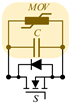 |
|
| RC |  |
|
| RCD |  |
|
| RCD + MOV | 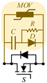 |
|
| Parameters | Acronym | Value | Unit |
|---|---|---|---|
| Input Voltage | 240 | ||
| Snubber Capacitor | 100 | ||
| Snubber Diode | 2 | ||
| Snubber Resistance | 22 | ||
| Line Inductor | 10 | ||
| Clamp voltage of MOV | 675 | ||
| MOSFETs | NTHL040N120SC1 | ||
| Capacitor of auxiliary circuit | 100 | ||
| Resistance of auxiliary circuit | 10 | k |
Publisher’s Note: MDPI stays neutral with regard to jurisdictional claims in published maps and institutional affiliations. |
© 2022 by the authors. Licensee MDPI, Basel, Switzerland. This article is an open access article distributed under the terms and conditions of the Creative Commons Attribution (CC BY) license (https://creativecommons.org/licenses/by/4.0/).
Share and Cite
Rahimpour, S.; Husev, O.; Vinnikov, D. Design and Analysis of a DC Solid-State Circuit Breaker for Residential Energy Router Application. Energies 2022, 15, 9434. https://doi.org/10.3390/en15249434
Rahimpour S, Husev O, Vinnikov D. Design and Analysis of a DC Solid-State Circuit Breaker for Residential Energy Router Application. Energies. 2022; 15(24):9434. https://doi.org/10.3390/en15249434
Chicago/Turabian StyleRahimpour, Saeed, Oleksandr Husev, and Dmitri Vinnikov. 2022. "Design and Analysis of a DC Solid-State Circuit Breaker for Residential Energy Router Application" Energies 15, no. 24: 9434. https://doi.org/10.3390/en15249434