Article

Optimized Design of Laminated Busbar for Large-Capacity Back-to-Back Converters

1
School of Electrical Engineering, Dalian University of Technology, Dalian 116024, China
2
CRRC Dalian R&D Co., Ltd., Dalian 116052, China
*
Author to whom correspondence should be addressed.
Energies 2022, 15(3), 774; https://doi.org/10.3390/en15030774
Submission received: 28 December 2021 / Revised: 13 January 2022 / Accepted: 17 January 2022 / Published: 21 January 2022
(This article belongs to the Section F: Electrical Engineering)

Abstract

:
As a key component of a large-capacity converter, the laminated busbar can improve the reliability, integration and power density of the converter and has great advantages in reducing the parasitic inductance of the switching loop. The laminated busbar suitable for a high-capacity back-to-back converter has a complex structure, and couple with each side converter. It has been challenging to optimize the equivalent inductance by using the traditional single-converter busbar design method. In this paper, the coupling inductance model of the back-to-back converter is established, and the relationship between the voltage stress of the switch tube and the stray inductance is analyzed in detail. Based on this, the design principle of the laminated busbar is proposed, and an optimized design structure of the laminated busbar suitable for the large-capacity back-to-back converter is given. Finally, the results were effectively verified by simulation analysis and a 180 kW integrated intermediate frequency auxiliary power converter.

1. Introduction

With the development of power electronic technology and semiconductor devices, large capacity, integration, high frequency and high power density have gradually become the development trends of power electronic converters [1,2,3]. Large-capacity converters are widely used in energy storage and grid connection [4], electric vehicles [5,6], solid-state transformers [7], high-speed rail [8] and other occasions.
Due to the high voltage and power level, the large volume of active and passive devices and the high requirement of insulation spacing, the overall dimensions of the converter are large. Traditional confluence methods, such as copper bars and cables, lead to large stray inductance into the converter circuit, affecting the reliability and stability of the device operation [9].
Compared with traditional connecting devices, laminated busbars with high reliability and low stray inductance have greater advantages in large-capacity and high-integration applications [10,11,12,13,14,15,16,17]. They can reduce the enclosed area of the commutation loop, effectively reduce the equivalent stray inductance and are easy to assemble, which is conducive to improving the power density of the converter. However, the laminated busbar structures applied to various converter topologies are quite different in terms of stray inductance, so the transient analysis of the laminated busbar stray parameters and the structural optimization design of the laminated busbar are important topics for high-capacity power electronic converters.
Based on the finite element analysis method, the influence of different laminated structures on busbar stray parameters can be analyzed quickly and accurately, and the current imbalance of parallel devices and the capacitance of absorption capacitors can be analyzed [15]. However, the interaction between stacked busbars and power devices in large power electronic converters deserves more attention, and it is difficult to achieve through finite element analysis. Meanwhile, the current research results focus on the analysis of the stray inductance of the double-layer busbar, and less on the evaluation of the stray inductance of the multi-layer busbar. With the wide application of multi-stage topologies [16,17], multiple parallel devices [15] and multilevel converters [18,19,20,21], the number of total bus layers has increased rapidly, and, therefore, it is necessary to study the stray parameter characteristics of multi-layer, complex busbars.
Compared with the laminated busbar connecting the bus capacitor and the single converter power module, limited studies focused on the multi-layer, DC laminated busbar structure shared by multiple converters. The design difficulty lies in the control decoupling between different converters. The existence of the middle bus capacitor makes the flow circuits of different side converters switch independently, but they are coupled with each other through the laminated bus, which needs to be analyzed separately. The laminated busbar is an effective method to reduce the stray inductance of the commutation loop, but the stray inductance of the laminated busbar is affected by the space structure of the power device’s placement. There are many different laminated busbar structures in the two-stage, back-to-back converter shared with the common DC bus, so it is necessary to analyze the stray inductance of the laminated busbar and the influence of the converter circuit coupling between converters under different spatial structures. Meanwhile, the parallel connection of multi-bus capacitors and power devices also affects the instantaneous current distribution of the switch in the laminated busbar.
Aiming at the auxiliary power supply for large-capacity, urban rail vehicles, this work focuses on the optimized design of laminated busbars suitable for large-capacity, back-to-back converters and proposes two methods to improve the switching voltage stress of back-to-back converters, which improves the reliability. In this paper, the coupled inductor model of the back-to-back converter is established, and the relationship between the switching voltage stress and the stray inductance is analyzed in detail. Further, the instantaneous current distribution of a multi-capacitor parallel bus is compared through theoretical analysis, and an optimized design structure of a laminated busbar suitable for large-capacity, back-to-back converters is given. Finally, a 180 kW integrated high frequency auxiliary power converter is designed, and the correctness of the theoretical analysis is verified by simulation analysis and double-pulse experiment.

2. Circuit Topology and Commutation Loop Analysis

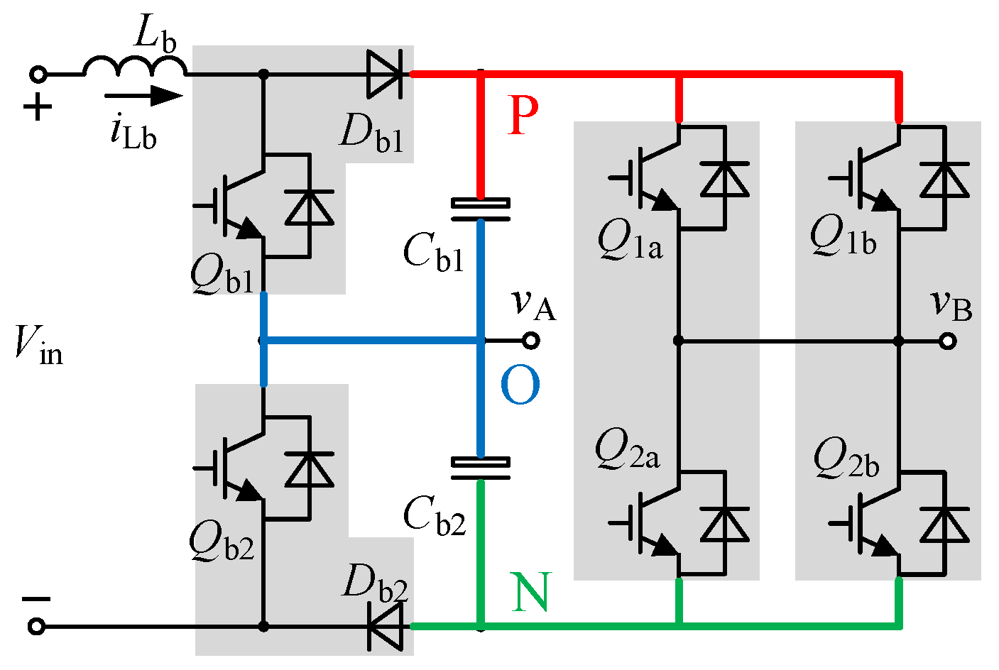
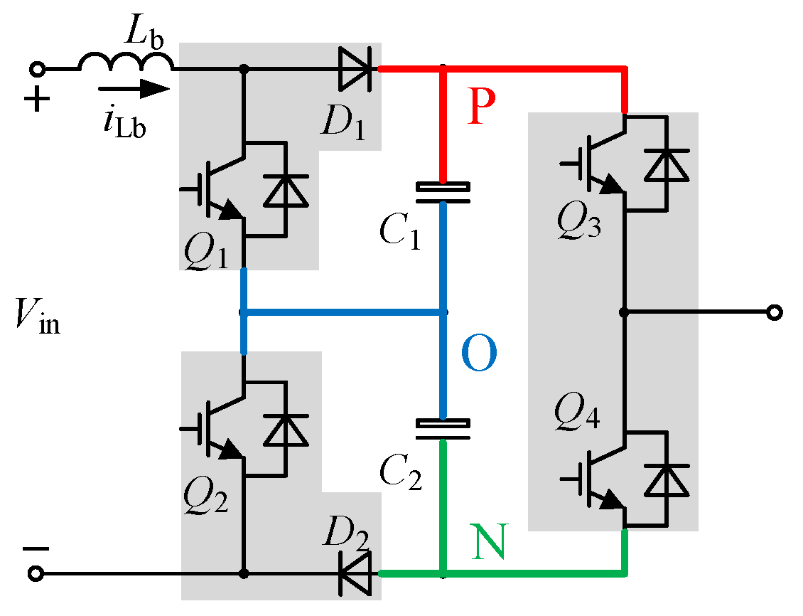
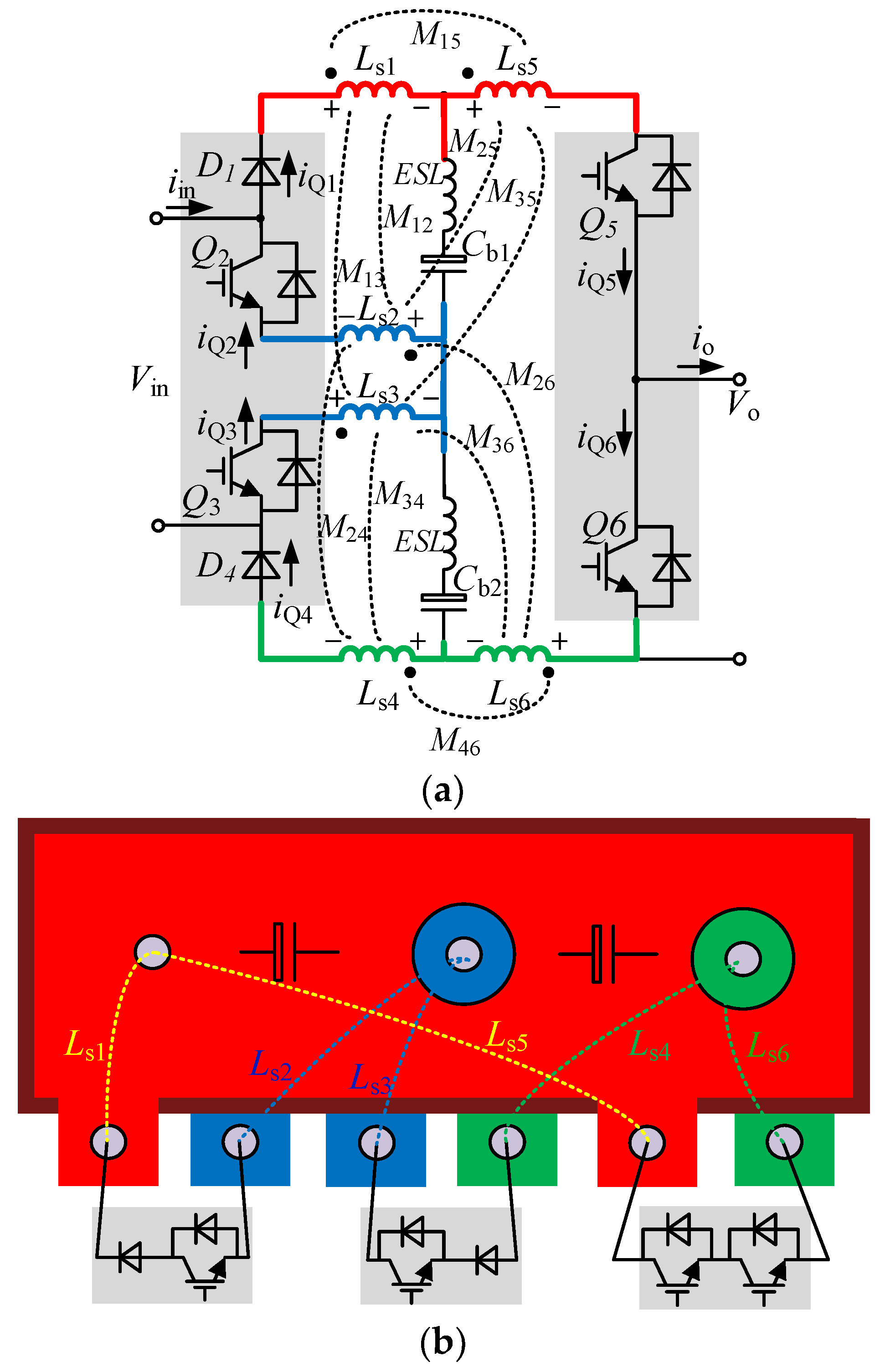
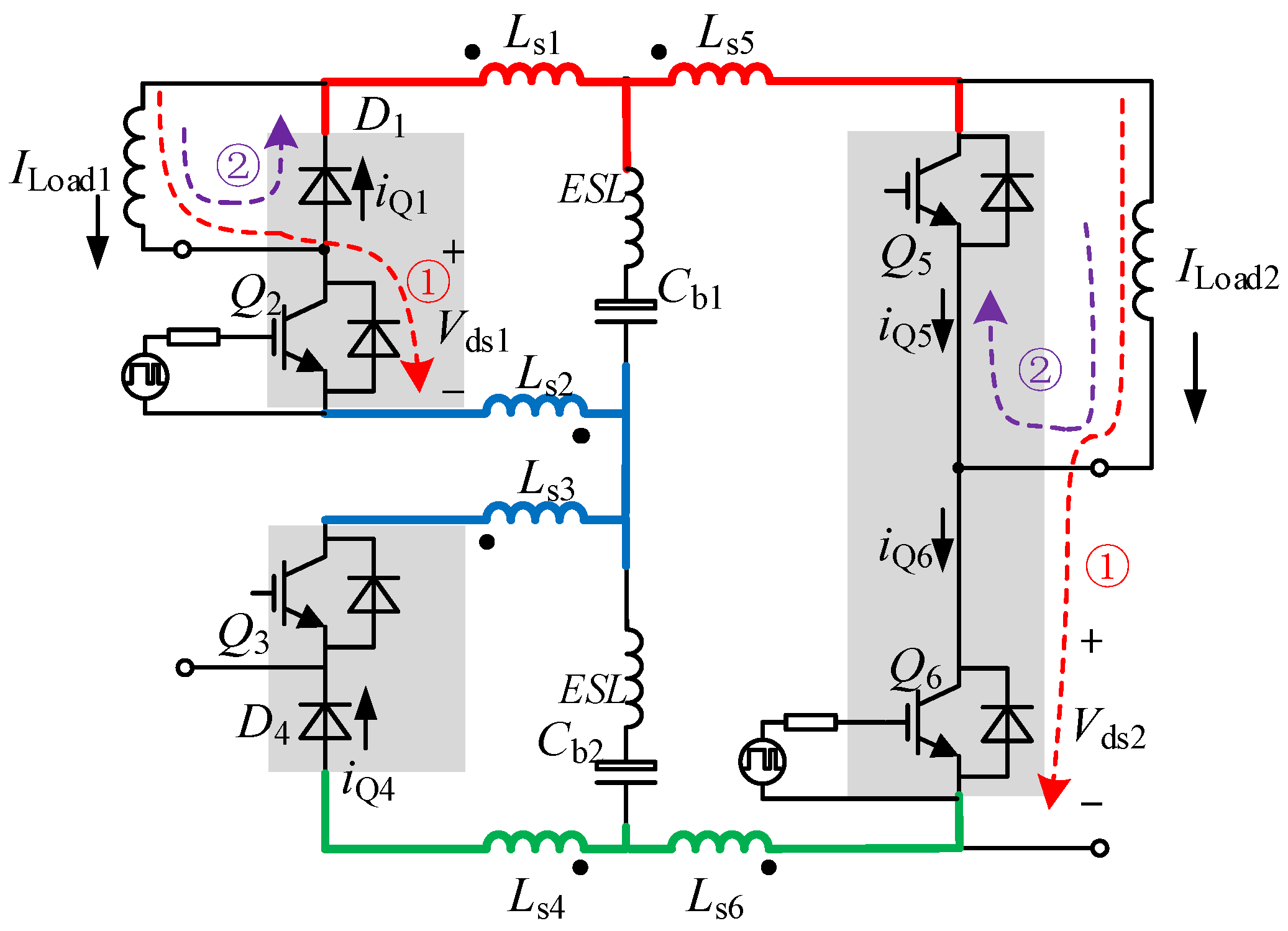
2.1. Auxiliary Power Supply Circuit Topology

As the power supply device of the train, the auxiliary power supply provides electric energy for the air conditioner, air compressor and DC load of the whole train, which is an important guarantee for the stable and safe operation of the train. Most of the existing auxiliary power supplies adopt the low-frequency transformer scheme, which is bulky and heavy, and the rectifier (DC110V) is not integrated in the three-phase inverter power supply. The power density of the auxiliary power supply is low, and the module design is scattered, which makes it difficult to meet the lightweight requirements of the current rail transit system in terms of weight and volume.
The novel large-capacity auxiliary power supply for urban rail vehicles adopts a high-frequency transformer isolation scheme, which reduces the weight and volume and improves the efficiency of the auxiliary power supply. The front stage adopts a three-level boost converter to reduce the input current ripple and reduce the noise and loss of the input reactor. The post-stage DC/DC converter converts the stable DC voltage into a high-frequency PWM voltage and sends it to the high-frequency transformers. Its topology is shown in Figure 1.
The three-level boost converter and the LLC converter are coupled through an intermediate DC bus to form a back-to-back converter. In order to reduce the commutation paths of multiple converter circuits, reduce their equivalent stray inductances and improve the power density of the novel auxiliary power supply, the DC bus connection of multiple converters is realized by using a laminated busbar. The laminated busbar is divided into a positive bus layer (P), a zero bus layer (O) and a negative bus layer (N), which are connected with two series half-bridges of the three-level boost circuit and the DC/DC converter, respectively. The distribution of the laminated bus is shown in Figure 2. The three-layer laminated busbar needs to be designed with a small commutation loop area to reduce the voltage spike of the switching tube, reduce the selection margin of the semiconductor device and ensure the safe and stable operation of the circuit.

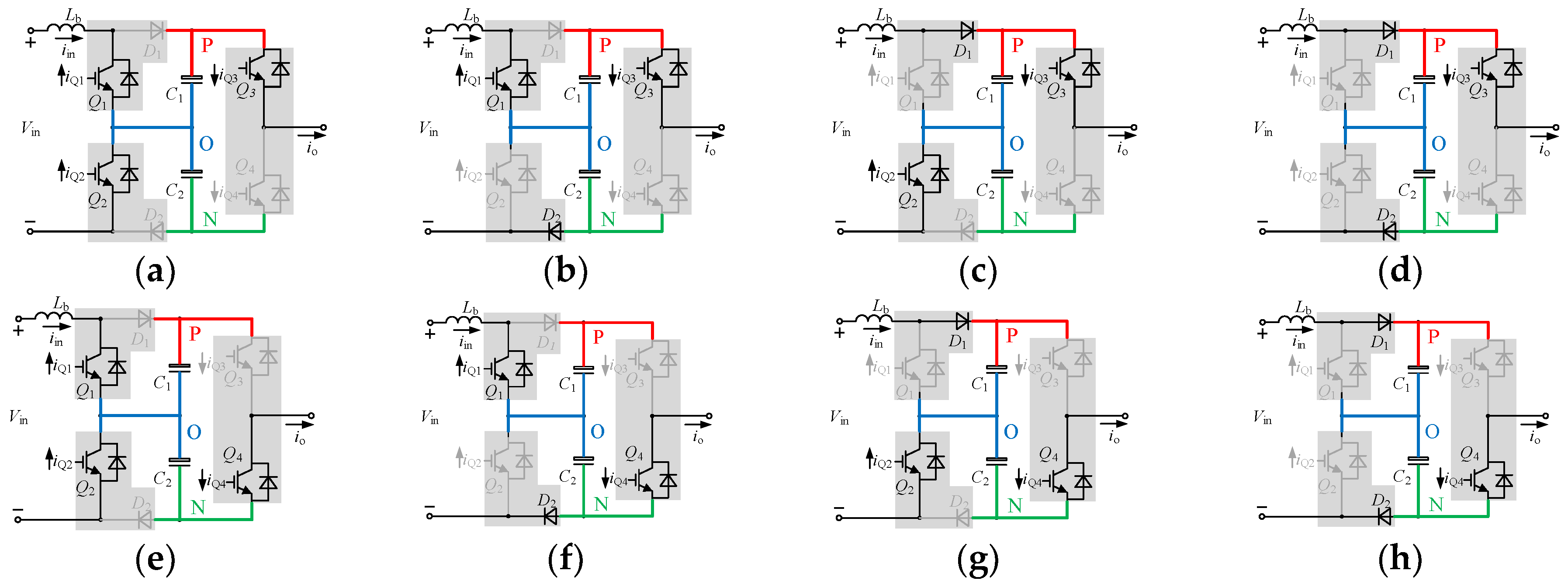
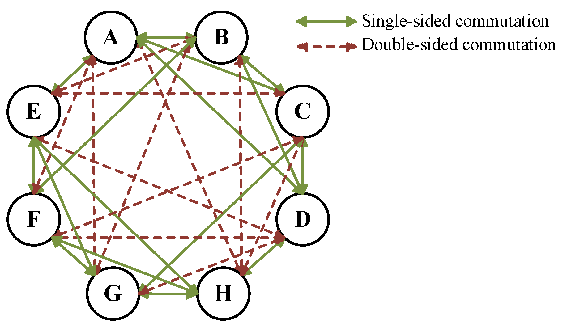
2.2. Circuit Loop Analysis

Compared with the laminated busbar connecting the bus capacitor and the single converter power module, the multi-layer, common DC laminated busbar structure for the multiple converters is more complicated. Furthermore, the coupling of commutation loops between different converters should be considered in the design.
First, we analyze the circulation loop and commutation path of the circuit topology, taking the back-to-back converter composed of three-level boost and half-bridge DC/DC as an example. As shown in Figure 3, Q1 and Q2 are IGBT of the front-stage converter, D1 and D2 are the front-stage diodes, Q3 and Q4 are IGBT of the post-stage converter, C1 and C2 are DC bus capacitors and P, N and O are the positive potential point, negative potential point and zero potential point of the DC bus, respectively.
According to the different switching states of the front stage and the post stage, there are eight kinds of circulation loop in the back-to-back converter. As shown in Figure 4, the arrow indicates the reference direction of the current. When the switching states are different, the input current iin and the output current io pass through the upper switching or the lower switching of the respective bridge to form different flow circuits. Due to the large value of the middle busbar capacitance, the capacitor voltages vC1 and vC2 can be regarded as constant in the switching period.
Each half-bridge circuit has two different commutation circuits, and the transient change time of the commutation circuit is uncertain so there is a situation wherein two half-bridge circuits are commutated at the same time. Therefore, it is necessary to consider the commutation loop current path and current stack area to analyze the influence of the stray inductance of different commutation loops.
Through the analysis of different commutation paths, there are 28 commutation processes in the back-to-back converter, as shown in Figure 5. Because the driving control of the front-stage bridge and the post-stage bridge is not related to each other, the commutation process of the converter can be divided into single-side commutation and double-side commutation, according to the instantaneous commutation situation. Single-sided commutation includes two cases of input-side, single-sided commutation and output-side, single-sided commutation. The voltage spike conditions of the three cases are different and need to be analyzed separately. As shown in Figure 5, the eight switching states change in the switching state machine. The circuit mainly contains one three-level bridge and one two-level bridge. The green color line means the change between two states only occurs in one bridge. However, the red color line means the change between two states occur in both bridges.

3. Analysis of Stray Inductance of Multi-Layer Busbar

This section first analyzes the stray inductance of the laminated busbar and then studies the relationship between the switch voltage stress and the stray inductance of the back-to-back converter. Finally, the influence of the parallel connection of multiple bus capacitors and power devices on the spatial structure of the components in the laminated busbar is analyzed.

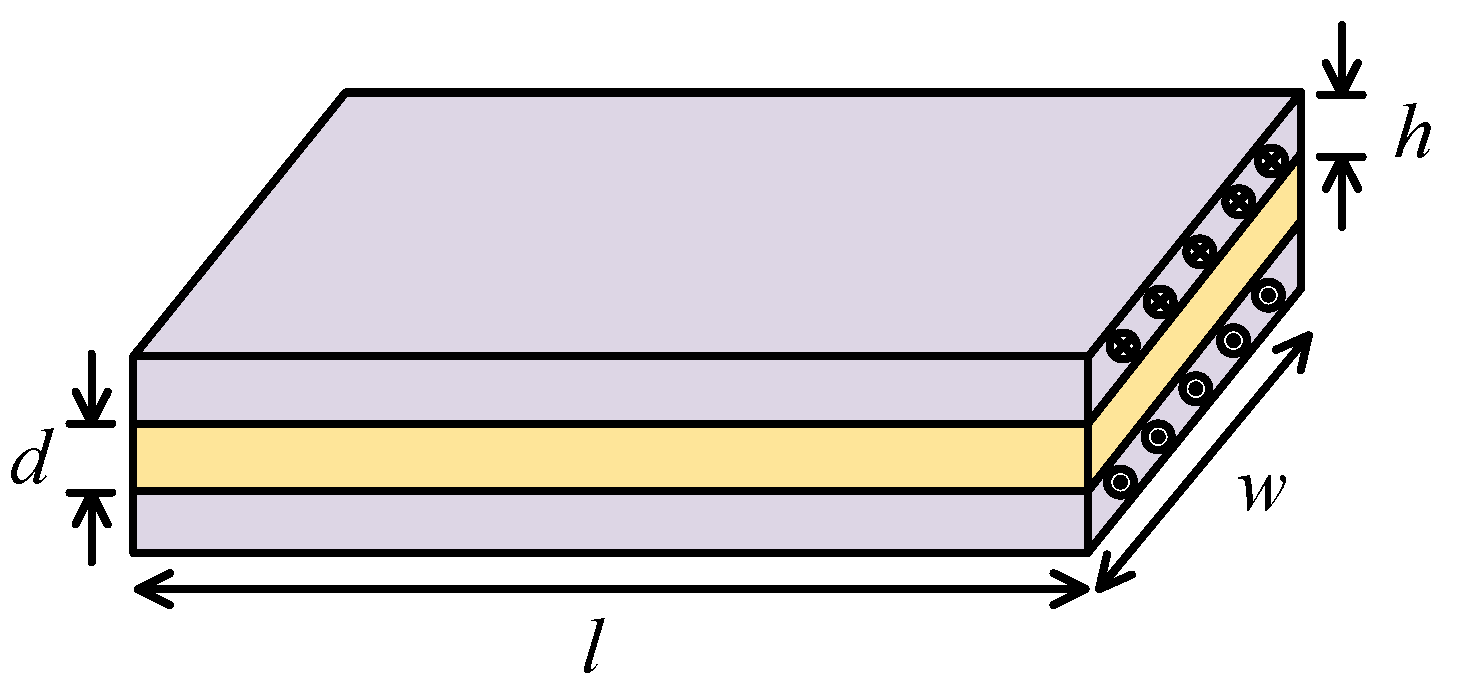
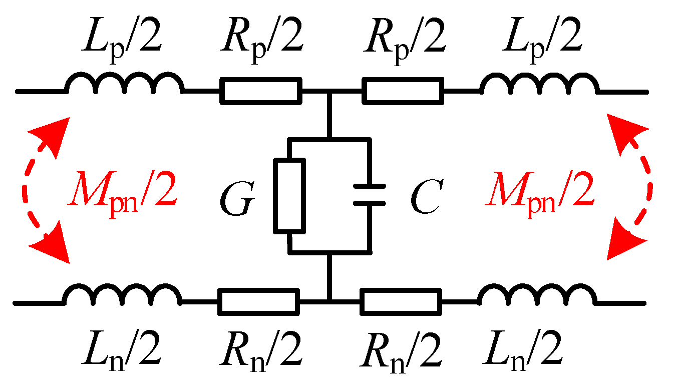
3.1. Stray Inductance Theory of Laminated Busbars

In order to suppress the transient voltage spike of the switch, a laminated busbar is usually used to reduce the stray inductance of each loop. Opposite currents flow between two adjacent conductors of the laminated busbar to generate mutual cancellation of electromagnetic fields, achieving the effect of low stray inductance. The structure model of the laminated busbar is shown in the Figure 6, where l is the length of the busbar, w is the width of the busbar, h is the thickness of the single-layer busbar and d is the insulation thickness.
According to the electromagnetic field theory, the stray inductance of the laminated busbar includes two parts: self-inductance and mutual inductance. Self-inductance can be divided into internal inductance and external inductance. The internal inductance is generated by the leakage flux commutation inside the conductor. The external inductance is formed by the closed magnetic field of the commutation loop and the interlinked magnetic field generated by the conductor layer current. The self-inductance of the laminated busbar can be expressed as [22]:
L self = μ 0 μ r l 8 π + 2 μ 0 μ r l π ln ( h h + w + 1 )
Among them, μ0 is the vacuum permeability and μr is the relative permeability.
When d << h and d + h << w, the self-inductance of the laminated busbar can be simplified as:
L self = μ 0 μ r l 8 π + 2 μ 0 μ r l h π ( h + w )
The mutual inductance between the two conductors of the laminated busbar can be expressed as [22]:
M = μ 0 μ r l h π 4 ( d + h ) 2 + k w 2 cos θ
Among them, d is the distance between the two conductor layers, k is the correction coefficient and θ is the angle between the two busbars. The electrical equivalent model of the double-stacked busbar is shown in Figure 7. Lp and Ln represent the equivalent self-inductance of the upper and lower conductor layers, Rp and Rn represent the equivalent resistance of the upper and lower conductor layers, Mpn is the equivalent mutual inductance of the two conductor layers, C is the equivalent capacitance and G is the conductivity.
In order to simplify the equivalent model, when analyzing the effect of stray inductance on the instantaneous voltage stress of the commutation loop, the effects of equivalent resistance, equivalent capacitance and conductivity are ignored. Therefore, the equivalent stray inductance of the laminated busbar is:
L eq = L p + L n - 2 M
Substituting Formulas (1)–(3) into Formula (4), the equivalent stray inductance of the laminated busbar can be expressed as:
L eq = μ 0 μ r l π ( 1 4 + 4 h h + w 2 h 4 ( d + h ) 2 + k w 2 cos θ )

3.2. Relationship between Switch Voltage Stress and Stray Inductance in Back-to-Back Converters

Inductive devices, such as inductors and transformers, connected to the midpoint of the input-side bridge or the output-side bridge, have current freewheeling capability. Because the switching period is very short, and the inductor current basically does not change in a short period of time, the input current iin and output current io of the back-to-back converter are considered to be constant during the switching of the current circuit; that is, diin/dt = dio/dt = 0, and the current passing through each switch tube should satisfy:
i in = i Q 1 i Q 2 = i Q 3 i Q 4 , d i Q 1 d t = d i Q 2 d t , d i Q 3 d t = d i Q 4 d t
i o = i Q 5 i Q 6 , d i Q 5 d t = d i Q 6 d t
Among them, iQ1, iQ2, iQ3, iQ4, iQ5 and iQ6 represent the currents of the power switches or diodes, as shown in Figure 8a.
Due to the small distance between the adjacent layers of the laminated busbar, there is a skin effect and proximity effect between the layers, and the current loop between the different layers also affects the current distribution of the other layer by coupled inductance. Therefore, the coupled inductance model of the laminated busbar of the half-bridge back-to-back converter is shown in Figure 8, where Ls1, Ls2, Ls3 and Ls4 represent the self-inductance from the connection point of the input-side switch to the connection point of the bus capacitor, and Ls5 and Ls6 represent the self-inductance from the connection points of the output-side switch to the connection points of the bus capacitor. M15 and M46 represent the mutual inductance between the through-flow circuits on the same busbar layer, and M12, M13, M25, M35, M23, M24, M26, M34 and M36 represent the mutual inductance between the through-flow circuits on different busbar layers. It is assumed that the mutual inductance between the uppermost layer and the lowermost layer in the laminated structure is ignored. Therefore, the relationship between the voltage, current and stray inductance on the bus can be expressed as:
[ v s 1 v s 2 v s 3 v s 4 v s 5 v s 6 ] = [ L s 1 M 12 M 13 0 M 15 0 M 21 L s 2 M 23 M 24 M 25 M 26 M 31 M 32 L s 3 M 34 M 35 M 36 0 M 42 M 43 L s 4 0 M 46 M 51 M 52 M 53 0 L s 5 0 0 M 62 M 63 M 64 0 L s 6 ] [ d i Q 1 d t d i Q 2 d t d i Q 3 d t d i Q 4 d t d i Q 5 d t d i Q 6 d t ]
Among them, vs1, vs2, vs3, vs4, vs5 and vs6 respectively represent the voltage between each connection point of the busbar. Combining Formulas (6) and (7), the relationship between voltage, current and stray inductance on the busbar can be simplified as:
[ v s 1 v s 2 v s 3 v s 4 v s 5 v s 6 ] = [ L s 1 + M 12 M 13 M 15 M 21 + L s 2 M 23 + M 24 M 25 + M 26 M 31 + M 32 L s 3 + M 34 M 35 + M 36 M 42 M 43 + L s 4 M 46 M 51 + M 52 M 53 L s 5 M 62 M 63 + M 64 L s 6 ] [ d i Q 1 d t d i Q 3 d t d i Q 5 d t ]
When the single-side commutation occurs at the input side, take the switching from the flow circuit A to the flow circuit B as an example. Only the input-side switch current is switched, and the switch current of the output-side bridge is kept constant; that is, when diQ1/dt = 0, diQ5/dt = diQ6/dt = 0 is combined with Formula (9), the switch voltage can be expressed as:
v Q 2 = v s 3 + v s 4 + v C 2 = ( L s 3 + L s 4 + M 34 + M 43 ) d i Q 3 d t + v C 2
When single-side commutation occurs at the output side, take the switching from the flow circuit A to the flow circuit E as an example. Only the output-side switch current is switched, and the switch current of the input-side bridge is kept constant; that is, when diQ1/dt = 0, diQ3/dt = 0 is combined with Formula (9), the switch voltage can be expressed as:
v Q 3 = v s 5 v s 6 + v C 1 + v C 2 = ( L s 5 + L s 6 ) d i Q 5 d t + v C 1 + v C 2
When double-sided commutation occurs, take the switching from the flow circuit A to the flow circuit F as an example. The switches generate current commutation on the input side and output side at the same time, and the switch voltage can be expressed as:
v Q 2 = v s 3 + v s 4 + v C 2 = ( L s 3 + L s 4 + M 34 + M 43 ) d i Q 3 d t + ( M 35 + M 36 + M 46 ) d i Q 5 d t + v C 2
v Q 3 = v s 5 v s 6 + v C 1 + v C 2 = ( M 53 + M 63 + M 64 ) d i Q 3 d t ( L s 5 + L s 6 ) d i Q 5 d t + v C 1 + v C 2
According to the switching voltage in the different commutation processes above, the voltage spike of the switch is not only related to the self-inductance and mutual inductance of the current circuit on one side, but also related to the mutual inductance between the current circuits on both sides. Therefore, reduce the surrounding area of the current circuit as much as possible so that the self-inductance and mutual inductance cancel each other to reduce the switching voltage spike. In addition, minimizing the overlapping area of the two-sides flow loops is the unique, laminated busbar optimization mode of the common DC bus back-to-back converter.

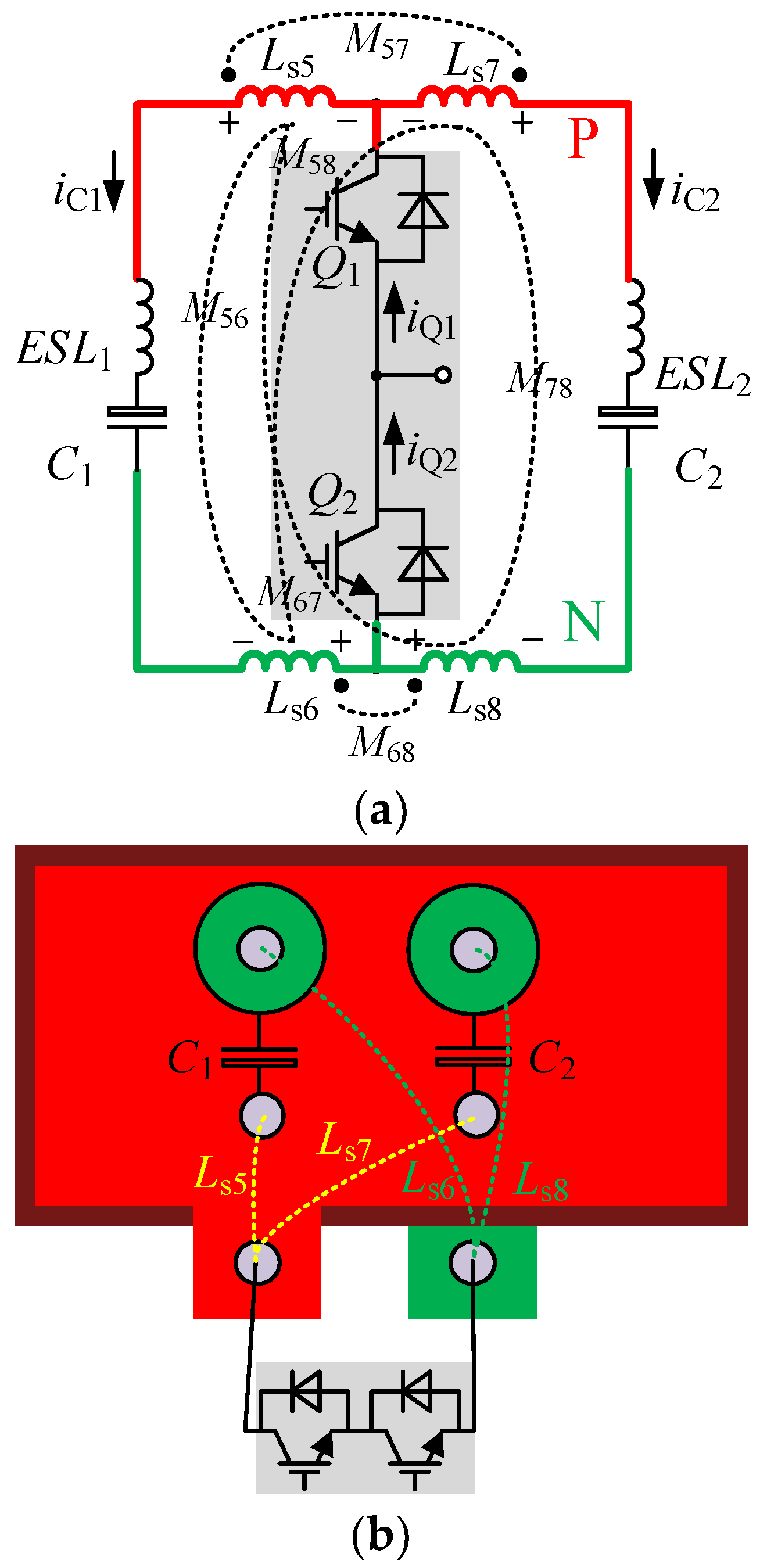
3.3. Analysis of Parallel Model of Multi-Bus Capacitors

In the application scenario of a back-to-back converter with multi-bus capacitors in parallel, the capacitor parallel affects the instantaneous current distribution of the switch in the laminated busbar so it is necessary to analyze the instantaneous current distribution of the multi-capacitor parallel busbar theoretically.
The coupled inductor circuit model of the multi-capacitor laminated busbar is shown in Figure 9a, where LS5 and LS6 represent the self-inductance of the switch connected to the bus capacitor C1 and LS7 and LS8 represent the self-inductance of the switch connected to the bus capacitor C2. M57 and M68 represent the mutual inductance between the same-layer through-flow circuits on the busbar, and M56, M58, M67 and M78 represent the mutual inductance between different-layer through-flow circuits.
Because the input current iin of the back-to-back converter is considered to be constant during the switching of the current circuit, diQ1/dt = diQ2/dt. Therefore, the derivative of the inductor current is 0 and diQ1/dt is equal to diQ2/dt. Meanwhile, considering the node of the three branches, the sum of the currents should be 0, and the current passing through each switch tube should satisfy:
i in = i Q 1 i Q 2 , d i Q 1 d t = d i Q 2 d t
i Q 1 = i C 1 + i C 6 , d i Q 1 d t = d i C 1 d t + d i C 2 d t
The current of switch tube and capacitor should meet:
d i Q 1 d t = d i Q 2 d t = d i C 1 d t + d i C 2 d t
Therefore, the relationship between voltage, current and stray inductance on the busbar can be expressed as:
[ v s 5 v s 6 v s 7 v s 8 ] = [ L s 5 + M 56 M 57 + M 58 M 65 + L s 6 M 67 + M 68 M 75 + M 76 L s 7 + M 78 M 85 + M 86 M 87 + L s 8 ] [ i C 1 d t i C 2 d t ]
Among them, vs5, vs6, vs7 and vs8 represent the voltage between the connection points of the busbar, respectively.
According to the circuit connection of the multi-capacitor laminated busbar, the voltage of the switch has the following relationship:
v Q 1 + v Q 3 = v C 1 v s 5 v s 6 = v C 2 v s 7 v s 8
Since the commutation time of the switch is extremely short compared to the discharge time of the capacitor, the voltages of the parallel capacitors can be considered equal; that is, vC1 = vC2. Formula (18) can be simplified:
  v s 5 + v s 6 = v s 7 + v s 8
Combined with Formula (17), the relationship between voltage, current and stray inductance on the busbar can be simplified as:
i C 1 d t i C 2 d t = L s 5 + L s 6 + 2 × M 56 M 57 M 58 M 67 M 68 L s 7 + L s 8 + 2 × M 78 M 57 M 58 M 67 M 68
From Formula (20), when the self-inductance and mutual inductance of each commutation circuit are the same, the instantaneous current distribution can be uniform, and the equivalent capacitance of the laminated busbar can be increased.
ANSYS can be used to simulate and analyze the characteristics of the laminated busbar with multiple bus capacitors in parallel. The laminated busbar with a single bus capacitor and three bus capacitors is simulated to obtain the top layer current distribution diagram of the two busbars, as shown in Figure 10.
Table 1 lists key parameters and the exploitation of the ANSYS model. There are two circles on the busbar to form a commutation loop. The distance between these two circles is 30 mm, considering a radius of 6 mm. In the three bus capacitors model, three capacitors are evenly distributed and 10 mm apart. A distance of 7 mm is set between the right circle of capacitor and the right edge of busbar. To calculate the capacitor of busbar, the solution type of magnetostatic is set, so there is no setting of frequency. Current excitation of the solid type is set to obtain a static magnetic field. The material of the busbar is copper with a relative permeability of 0.999991 and a bulk conductivity of 5.8 × 10⁷ siemens/m. An air sphere of a 140 mm radius is set as the calculation region.
By comparing the current distribution, it can be found that the current density of the multi-capacitor laminated busbar at the connection point of the power devices is smaller, and the current distribution on the whole laminated busbar is more uniform.
When a single bus capacitor is used, the stray inductance of the commutation loop is approximately 7.506 nH; when three bus capacitors are used, the stray inductance of the commutation loop is approximately 5.629 nH. Compared with the single-capacitor structure, the three-capacitor structure reduces the stray inductance by 25%. Meanwhile, as the number of intermediate bus capacitors increases, the stray inductance of the commutation loop decreases, and the consistency of each capacitor branch is better.

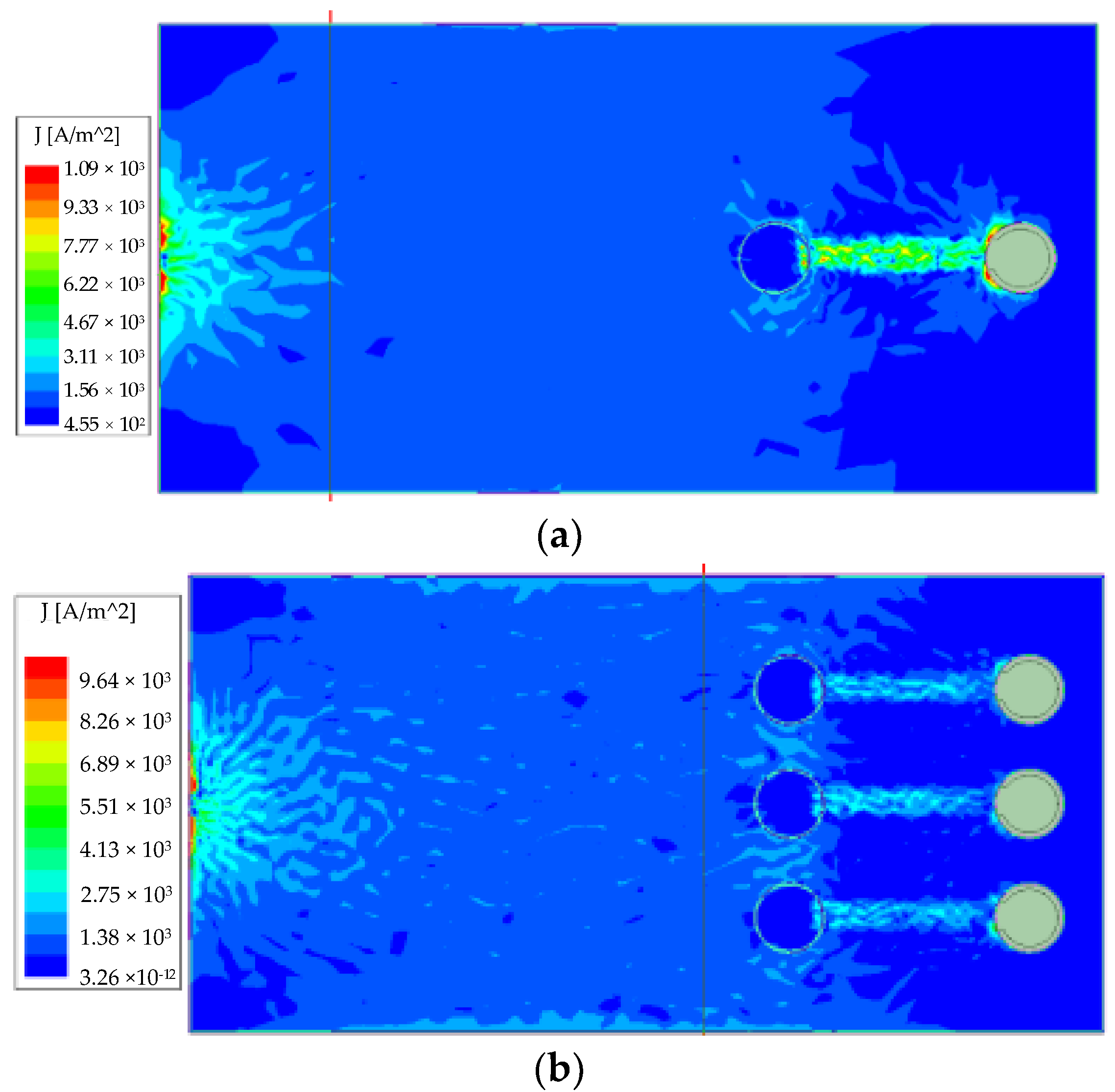
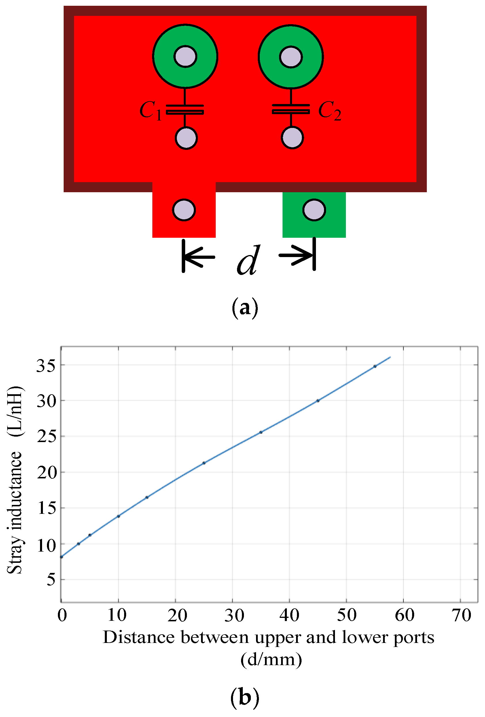
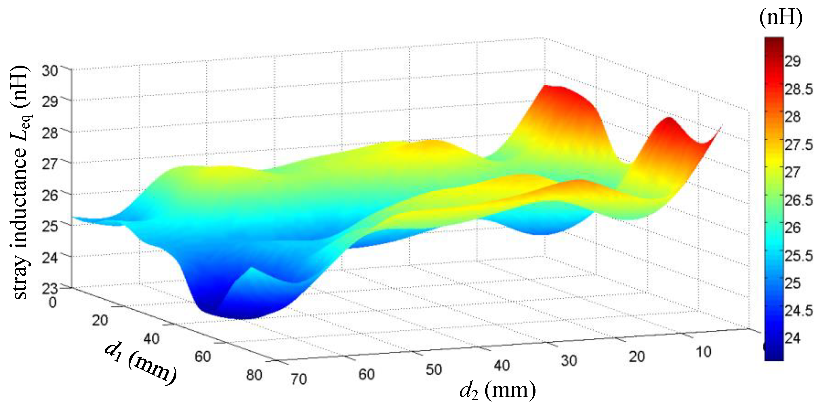
3.4. Relationship between Connection Point Spacing and Stray Inductance

The distance between the two connection points of the power module is closely related to the stray inductance and needs to be analyzed. Through ANSYS simulation analysis, the stray inductance value of the commutation loop under different connection point distances is obtained, and the relationship diagram is shown in Figure 11. It can be seen that, as the distance between the connection points of the power module increases, the stray inductance of the commutation loop is increasing. At 55 mm, the stray inductance is about 35 nH, which is 4.67 times that of the overlapping connection points. The simulation results are consistent with the mechanism of stray inductance. The larger the area enclosed by the commutation loop, the larger the stray inductance. Therefore, when designing the laminated busbar structure, it is necessary to ensure that the distance between the two connection points of the power module is as small as possible and the overlapping structure is optimal.

3.5. Optimization Principle of Laminated Busbar

According to the analysis of the topological structure and stray inductance of the laminated busbar of the back-to-back converter, the structure of the laminated busbar needs to:
(1)
Reduce the stray inductance of the current flow loop at this side, which is consistent with the conventional way of improving the characteristics of the laminated busbar, and reduce the surrounding area of the current circuit as much as possible so that the self-inductance and mutual inductance cancel each other to reduce the switching voltage spike;
(2)
Reduce the stray inductance caused by the mutual inductance between the two sides of the flow loops and minimizing the overlapping area of the two-sides flow loops via the unique laminated busbar optimization mode of the common DC bus back-to-back converter;
(3)
Select a laminated busbar with multiple bus capacitors in parallel to reduce the stray inductance of the commutation loop, considering the length of the laminated busbar and the number of power modules.

4. Design and Verification

In this section, according to the above optimization design principles of the laminated busbars, the design and simulation of the laminated busbar prototype and the dynamic characteristics test of the laminated busbar are carried out so as to verify the feasibility and rationality of the design of the laminated busbars.

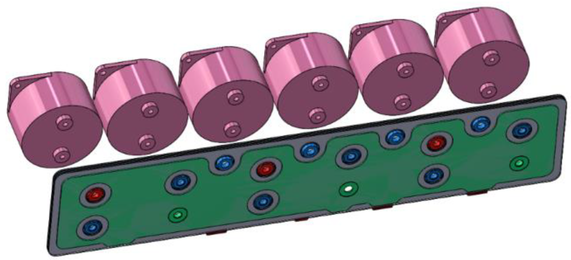
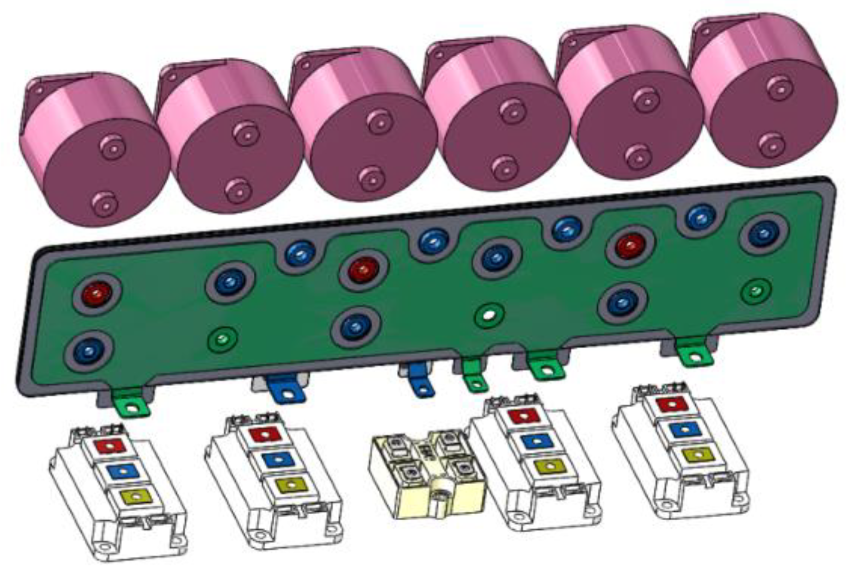
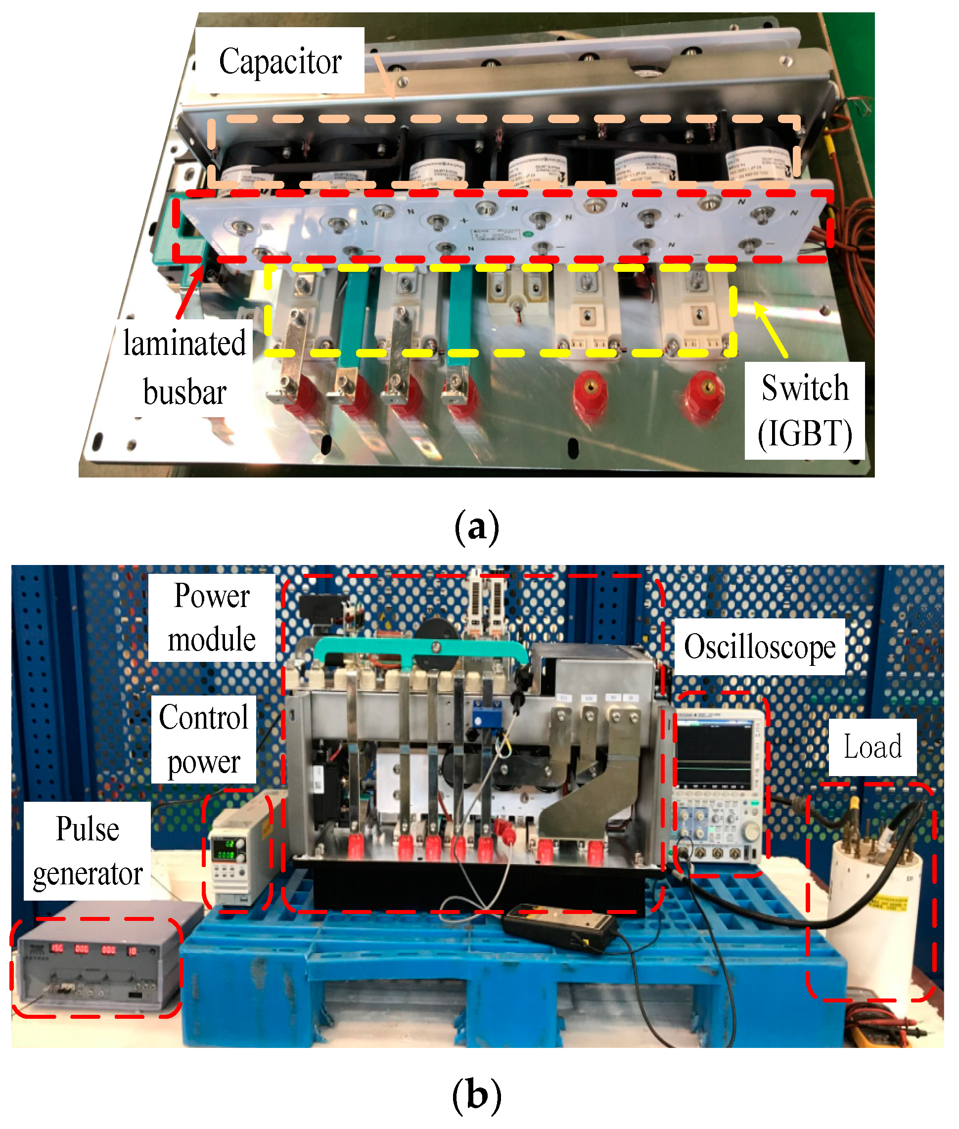
4.1. Optimal Design and Simulation of Laminated Busbar

Based on the above analysis, the number of bus capacitors is selected according to the structure space and circuit characteristics, and the capacitance distribution of laminated busbar is shown in Figure 12.
The stray inductance of the switch tube in the loop is affected by the connection position of the switch, as shown in Figure 13. The influence of distances d1 and d2 on the stray inductance of the loop is analyzed by the ANSYS simulation software. Considering the limitation of converter device placement, the adjustable range of d1 and d2 is less than 70 mm (0 < d1 < 70 mm, 0 < d2 < 70 mm), where LON, LPO, LPN1 and LPN2 respectively represent the busbar stray inductance of each switching loop.
Through the ANSYS simulation, the busbar stray inductances LON, LPO, LPN1 and LPN2 of each switching at different distances d1 and d2 can be calculated. So, four functions (LON(d1, d2), LPO(d1, d2), LPN1(d1, d2) and LPN2(d1, d2)) with variables d1 and d2 can be described, and a mean value function Leq(d1, d2) of the four functions (LON(d1, d2), LPO(d1, d2), LPN1(d1, d2) and LPN2(d1, d2)) is constructed. The variables (d1, d2) corresponding to the minimum of the function Leq(d1, d2) are considered to be the optimal values.
In order to optimize the stray inductance of the laminated busbar, the strategy of Formula (21) is used for parameter optimization.
L eq ( d 1 , d 2 ) = s u m ( L PO ( d 1 , d 2 ) + L ON ( d 1 , d 2 ) + L PN 1 ( d 1 , d 2 ) + L PN 2 ( d 1 , d 2 ) ) 4
According to Formula (21), the relationship between the distances d1 and d2 and the equivalent stray inductance Leq is obtained, as shown in Figure 14. It can be seen that the minimum value of Leq is 23.56 nH when d1 and d2 is (57 mm, 65 mm). The stray inductance is reduced by 19.6% compared to the highest value of 29.3 nH.
With the parameters d1 and d2 determined, the three-dimensional diagram and layered schematic diagram of the adopted laminated busbar used are shown in Figure 15. Its features include: considering the relationship between the length of the power module and the diameter of the capacitor, three groups of capacitors are selected in parallel to reduce the miscellaneous dispersion inductance; the upper bus capacitor and the lower bus capacitor are arranged at intervals to make the enclosed area of each commutation circuit relatively balanced; the power modules on both sides of the back-to-back converter are placed separately to reduce the overlap area of the current circuits on both sides and reduce mutual inductance between the flow loops on both sides; the two connection points of each power module adopt a corner connection method to minimize the distance in the horizontal direction.
Based on the above points, the prototype design based on the laminated busbar is shown by the exploded view in Figure 16.

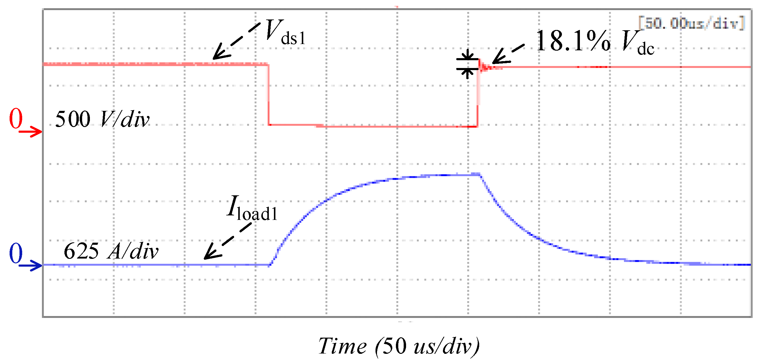
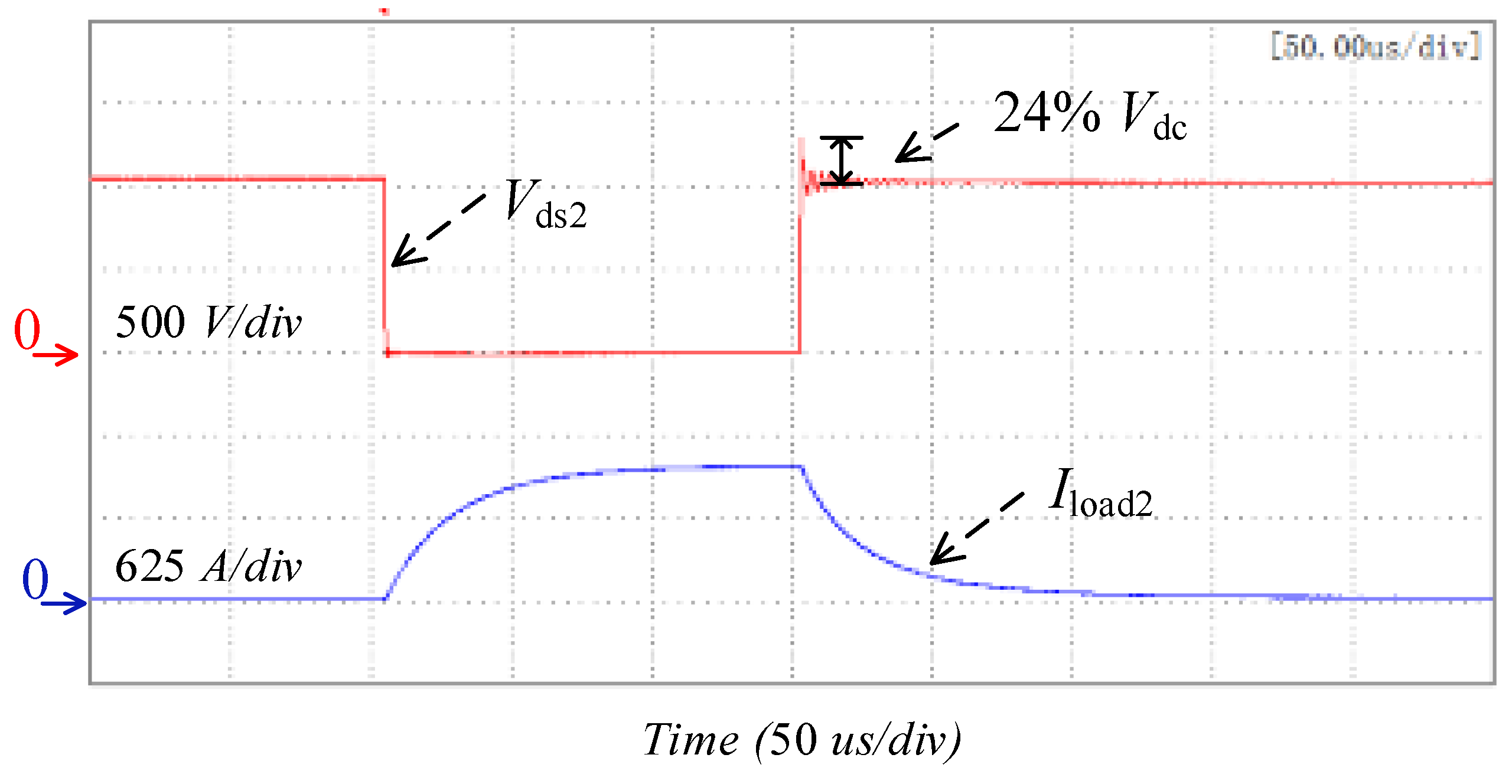
4.2. Dynamic Characteristic Test

In order to verify the effect of the designed, low-inductance laminated busbar on reducing the loop stray inductance and device voltage spike, a test platform is needed to test the dynamic characteristics of the laminated busbar. A dynamic pulse experiment is used to test the switching characteristics of the three-level boost circuit and LLC circuit, and the test principle circuit is shown in Figure 17. The current switching path of the pulse test is shown in ① and ②. The key parameters of the dynamic pulse test circuit are listed in Table 2. The pulse generator generates pulse signals for testing. The working condition is 1000 V/1000 A.
Figure 18a is the real dynamic characteristic test object of the laminated busbar. Figure 18b shows the pulse test platform of the back-to-back converter circuit, including the control power supply, pulse generator, oscilloscope, load and power supply to be tested.
The voltage level of the three-level boost circuit power module (SKM400GAL125, SKM400GAR125) is 1200 V and the test bus voltage is 750 V. From the switching process in Figure 19, the switch turn-off voltage spike is 886 V, and the Vdc voltage overshoot is 18.1% of the bus voltage. The voltage level of the LLC circuit power module (SKM400GB176D) is 1700 V and test bus voltage is 1000 V. From the switching process in Figure 20, the switch tube turn-off voltage spike is 1240 V, the Vdc voltage overshoot is 24% of the bus voltage and the voltage safety margin is 27.1%. Both can effectively avoid the device loss caused by circuit crosstalk and stray inductance and improve safety and reliability.
It can be seen that the switching oscillation of power devices is smaller and the voltage spike is lower by using the laminated busbar with optimized structure, and the effect of the designed, low-inductance laminated busbar on reducing the loop stray inductance and device voltage spike is verified.

5. Conclusions and Future Work

The paper first analyzes the new auxiliary power supply topology of the train and then establishes the coupled inductance model of the back-to-back converter laminated busbar. The relationship between the switch voltage stress and the stray inductance is analyzed in detail, and methods to improve the switch voltage stress of back-to-back converter are proposed. Finally, an optimized design structure of laminated busbar for large-capacity, back-to-back converters is presented. The work of the thesis resulted in the following conclusions:
(1)
It establishes the coupled inductance model of the laminated busbar of the back-to-back converter and gives measures to improve the voltage stress of the power device: reduce the enclosing area of the current flow loop so that the self-inductance and mutual inductance cancel each other; reduce the two overlap areas of the one-side flow loops; and reduce the mutual inductance between the flow loops on both sides;
(2)
An optimized design structure of laminated busbars suitable for large-capacity, back-to-back converters is given.
(3)
A set of 180 kW train high frequency auxiliary power converters is designed, and the pulse experiment verifies the safety and reliability of the theoretical analysis.
In future research, more granular design and optimization of laminated busbars can rely on neural network algorithms such as the ANN approaches [23] for modeling and an ordinary PSO [24] for parameter optimization.

Author Contributions

Conceptualization, M.X. and N.W.; methodology, M.X. and N.W.; validation, M.X. and Z.W.; formal analysis, M.X.; writing—original draft preparation, M.X.; writing—review and editing, N.W. and Z.W.; project administration, N.W. All authors have read and agreed to the published version of the manuscript.

Funding

This research received no external funding.

Institutional Review Board Statement

Not applicable.

Informed Consent Statement

Not applicable.

Data Availability Statement

Not applicable.

Conflicts of Interest

The authors declare no conflict of interest.

References

  1. Schiestl, M.; Marcolini, F.; Incurvati, M.; Capponi, F.G.; Starz, R.; Caricchi, F.; Rodriguez, A.S.; Wild, L. Development of a High Power Density Drive System for Unmanned Aerial Vehicles. IEEE Trans. Power Electron. 2020, 36, 3159–3171. [Google Scholar] [CrossRef]
  2. Lee, H.; Smet, V.; Tummala, R. A Review of SiC Power Module Packaging Technologies: Challenges, Advances, and Emerging Issues. IEEE J. Emerg. Sel. Top. Power Electron. 2020, 8, 239–255. [Google Scholar] [CrossRef]
  3. Chen, J.; Du, X.; Luo, Q.; Zhang, X.; Sun, P.; Zhou, L. A Review of Switching Oscillations of Wide Bandgap Semiconductor Devices. IEEE Trans. Power Electron. 2020, 35, 13182–13199. [Google Scholar] [CrossRef]
  4. Dongye, Z.; Qi, L.; Liu, K.; Wei, X.; Cui, X. Coupled Inductance Model of Full-Bridge Modules in Hybrid High Voltage Direct Current Circuit Breakers. IEEE Trans. Ind. Electron. 2019, 67, 10315–10324. [Google Scholar] [CrossRef]
  5. Wang, K.; Wang, L.; Yang, X.; Zeng, X.; Chen, W.; Li, H. A Multiloop Method for Minimization of Parasitic Inductance in GaN-Based High-Frequency DC–DC Converter. IEEE Trans. Power Electron. 2017, 32, 4728–4740. [Google Scholar] [CrossRef]
  6. Moorthy, R.S.K.; Aberg, B.; Olimmah, M.; Yang, L.; Rahman, D.; Lemmon, A.N.; Yu, W.; Husain, I.; Sree, K.R. Estimation, Minimization, and Validation of Commutation Loop Inductance for a 135-kW SiC EV Traction Inverter. IEEE J. Emerg. Sel. Top. Power Electron. 2019, 8, 286–297. [Google Scholar] [CrossRef]
  7. Xie, Y.; Bingyang, L.; Hongkeng, Z.; Jiwen, W.; Kangping, W.; Xu, Y.; Laily, W. Optimization of Laminated Busbar for Three-Level NPC Topology Using SiC Module. In Proceedings of the 2020 IEEE 9th International Power Electronics and Motion Control Conference (IPEMC2020-ECCE Asia), Nanjing, China, 29 November–2 December 2020; pp. 302–307. [Google Scholar]
  8. Zhang, N.; Wang, S.; Zhao, H. Develop Parasitic Inductance Model for the Planar Busbar of an IGBT H Bridge in a Power Inverter. IEEE Trans. Power Electron. 2015, 30, 6924–6933. [Google Scholar] [CrossRef]
  9. Wang, J.; Shaolin, Y.; Zhang, X. Effect of key physical structures on the laminated bus bar inductance. In Proceedings of the 2016 IEEE 8th International Power Electronics and Motion Control Conference (IPEMC-ECCE Asia), Hefei, China, 22–26 May 2016; pp. 3689–3694. [Google Scholar]
  10. Geng, C.; He, F.; Zhang, J.; Hu, H. Partial Stray Inductance Modeling and Measuring of Asymmetrical Parallel Branches on the Bus-Bar of Electric Vehicles. Energies 2017, 10, 1519. [Google Scholar] [CrossRef] [Green Version]
  11. Zhang, Z.; Liu, C.; Wang, M.; Si, Y.; Liu, Y.; Lei, Q. High-Efficiency High-Power-Density CLLC Resonant Converter with Low-Stray-Capacitance and Well-Heat-Dissipated Planar Transformer for EV On-Board Charger. IEEE Trans. Power Electron. 2020, 35, 10831–10851. [Google Scholar] [CrossRef]
  12. Plesca, A. Thermal Analysis of Busbars from a High Current Power Supply System. Energies 2019, 12, 2288. [Google Scholar] [CrossRef] [Green Version]
  13. Liang, Z.; Hu, S.; Wang, M.; He, X. DC-Link Busbar Network Design and Evaluation Method for the Large-Capacity Power Electronic Converter. IEEE J. Emerg. Sel. Top. Power Electron. 2021, 9, 4137–4145. [Google Scholar] [CrossRef]
  14. Liu, B.; Li, W.; Meng, D.; Diao, L.; Ma, Y.; Qiu, T.; Diao, L. Low-stray inductance optimized design for power circuit of SiC-MOSFET-Based inverter. IEEE Access 2020, 8, 20749–20758. [Google Scholar] [CrossRef]
  15. Zhang, B.; Wang, S. Parasitic Inductance Modeling and Reduction for Wire-Bonded Half-Bridge SiC Multichip Power Modules. IEEE Trans. Power Electron. 2021, 36, 5892–5903A. [Google Scholar] [CrossRef]
  16. Deshpande, A.; Luo, F. Multilayer busbar design for a Si IGBT and SiC MOSFET hybrid switch based 100 kW three-level T-type PEBB. In Proceedings of the 2017 IEEE 5th Workshop on Wide Bandgap Power Devices and Applications (WiPDA), Albuquerque, NM, USA, 30 October–1 November 2017; pp. 20–24. [Google Scholar]
  17. Zou, G.; Zhao, Z.; Yuan, L. Study on DC busbar structure considering stray inductance for the back-to-back IGBT-based converter. In Proceedings of the 2013 Twenty-Eighth Annual IEEE Applied Power Electronics Conference and Exposition (APEC), Long Beach, CA, USA, 17–21 March 2013; pp. 1213–1218. [Google Scholar]
  18. Liu, B.; Ren, R.; Jones, E.A.; Gui, H.; Zhang, Z.; Chen, R.; Wang, F.; Costinett, D. Effects of Junction Capacitances and Commutation Loops Associated with Line-Frequency Devices in Three-Level AC/DC Converters. IEEE Trans. Power Electron. 2018, 34, 6155–6170. [Google Scholar] [CrossRef]
  19. Gui, H.; Chen, R.; Zhang, Z.; Niu, J.; Tolbert, L.M.; Wang, F.; Costinett, D.; Blalock, B.J.; Choi, B.B. Methodology of Low Inductance Busbar Design for Three-Level Converters. IEEE J. Emerg. Sel. Top. Power Electron. 2021, 9, 3468–3478. [Google Scholar] [CrossRef]
  20. Yuan, Z.; Peng, H.; Deshpande, A.; Narayanasamy, B.; Emon, A.I.; Luo, F.; Chen, C. Design and Evaluation of Laminated Busbar for Three-Level T-Type NPC Power Electronics Building Block With Enhanced Dynamic Current Sharing. IEEE J. Emerg. Sel. Top. Power Electron. 2019, 8, 395–406. [Google Scholar] [CrossRef]
  21. Smirnova, L.; Juntunen, R.; Murashko, K.; Musikka, T.; Pyrhonen, J. Thermal Analysis of the Laminated Busbar System of a Multilevel Converter. IEEE Trans. Power Electron. 2015, 31, 1479–1488. [Google Scholar] [CrossRef]
  22. Mehrabadi, N.R.; Cvetkovic, I.; Wang, J.; Burgos, R.; Boroyevich, D. Busbar design for SiC-based H-bridge PEBB using 1.7 kV, 400 a SiC MOSFETs operating at 100 kHz. In Proceedings of the IEEE Energy Conversion Congress and Exposition (ECCE), Milwaukee, WI, USA, 18–22 September 2016; pp. 1–7. [Google Scholar]
  23. Nguyen, T.V.; Wong, R.K.W.; Hegde, C. Benefits of Jointly Training Autoencoders: An Improved Neural Tangent Kernel Analysis. IEEE Trans. Inf. Theory 2021, 67, 4669–4692. [Google Scholar] [CrossRef]
  24. Fan, S.; Hsu, C.Y.; Jen, C.H.; Chen, C.L.; Juan, L.-T. Defective wafer detection using a denoising autoencoder for semiconductor manufacturing processes. Adv. Eng. Inform. 2020, 46, 101166. [Google Scholar] [CrossRef]
Figure 1. Novel auxiliary power supply for urban rail transit train.
Energies 15 00774 g001
Figure 2. Laminated busbar distribution of DC bus in back-to-back converter.
Energies 15 00774 g002
Figure 3. Circuit topology of back-to-back converter.
Energies 15 00774 g003
Figure 4. Flow path of back-to-back converter. (a) Path A. (b) Path B. (c) Path C. (d) Path D. (e) Path E. (f) Path F. (g) Path G. (h) Path H.
Energies 15 00774 g004
Figure 5. Commutation process of back-to-back converter. (The meanings of A, B, C, D, E, F, G, H, are shown in Figure 4).
Energies 15 00774 g005
Figure 6. Laminated busbar structure model.
Energies 15 00774 g006
Figure 7. Equivalent model of laminated busbar circuit.
Energies 15 00774 g007
Figure 8. Coupled inductance model of back-to-back converter’s middle bus laminated busbar. (a) Coupled inductor circuit model, (b) schematic diagram of stray inductance of laminated busbar.
Energies 15 00774 g008
Figure 9. Coupled inductance model of multi-bus capacitor parallel laminated busbar. (a) Coupled inductor circuit model (b) Schematic diagram of stray inductance of laminated busbar.
Energies 15 00774 g009
Figure 10. Current distribution diagram of multi-bus capacitor parallel laminated busbar. (a) Single bus capacitor. (b) Three bus capacitors.
Energies 15 00774 g010
Figure 11. Relationship between stray inductance and connection point distance of laminated busbar. (a) The distance between the two connection points. (b) Stray inductance curve with distance d.
Energies 15 00774 g011
Figure 12. The capacitance distribution of laminated busbar.
Energies 15 00774 g012
Figure 13. Distance description diagram of switch position.
Energies 15 00774 g013
Figure 14. The relationship between the distances d1 and d2 and the equivalent stray inductance.
Energies 15 00774 g014
Figure 15. The three-dimensional diagram and layering diagram of the used laminated busbar. (a) Three-dimensional map. (b) Layered schematic.
Energies 15 00774 g015
Figure 16. The exploded diagram of laminated busbar, switches and capacitors.
Energies 15 00774 g016
Figure 17. Dynamic pulse test circuit.
Energies 15 00774 g017
Figure 18. Novel auxiliary power circuit and experimental platform. (a) Laminated busbar prototype. (b) Experiment platform.
Energies 15 00774 g018
Figure 19. Switching dynamic characteristic test of three-level boost circuit power module.
Energies 15 00774 g019
Figure 20. Switching dynamic characteristic test of LLC circuit power module.
Energies 15 00774 g020
Table 1. Key parameters and exploitation of the ANSYS model.
ParameterValue
Length of busbar160 mm
Width of busbar80 mm
Thickness of busbar1 mm
Radius of calculation region circle140 mm
Radius of bus capacitor6 mm
Table 2. Key parameters of the dynamic pulse test circuit.
ParameterValue
D1, Q2SKM400GAL125
Q3, D4SKM400GAR125
Q5, Q6SKM400GB176D
Time of Pulse Width150 us
Maximum load test current 1000 A
Publisher’s Note: MDPI stays neutral with regard to jurisdictional claims in published maps and institutional affiliations.

