Article

Dual-Domain Maximum Power Tracking for Multi-Input RF Energy Harvesting with a Reconfigurable Rectifier Array

Department of Electrical Engineering, National Chung Cheng University, Chaiyi 62102, Taiwan
*
Author to whom correspondence should be addressed.
Energies 2022, 15(6), 2068; https://doi.org/10.3390/en15062068
Submission received: 12 February 2022 / Revised: 7 March 2022 / Accepted: 10 March 2022 / Published: 11 March 2022
(This article belongs to the Special Issue Energy Harvesting Circuits and Systems for Low-Power IoT Devices)

Abstract

:
This work proposes a dual-domain maximum power tracking (MPPT) technique for multiple-input RF energy harvesting systems. A differential rectifier array is used to implement 4-channel reconfigurable RF to DC power conversion, and an adjustable 4-bit capacitor array is designed to improve the impedance matching between the antennas and the rectifiers. Using the perturbation and observation (P&O) method, both arrays are adaptively configured in the background with the variations of the input energy and output loading. Experimental results show that the proposed circuit successfully tracks the maximum power points while harvesting RF energy, with the peak conversion efficiency of 49.06% when the input energy is −6 dBm. With the proposed dual-domain MPPT, the high efficiency range of the energy harvesting system is greatly extended to 21 dB (−21–0 dBm).

1. Introduction

With the continuously advancing wireless communication technologies, internet of things (IoTs) is becoming popular in many new applications nowadays. Devices with various sensing techniques, such as temperature, illumination, pressure, and humidity sensing, are commonly used in buildings, industrial controls, health monitoring, and smart home appliances [1,2,3,4,5]. Figure 1 shows the smart home system with IoTs, which usually consists of dozens to hundreds of wireless sensor nodes. Due to the large number of sensor nodes, the maintenance cost will significantly increase to replace the batteries on a regular basis. Moreover, the batteries typically occupy a considerable portion of the system volume and weight. Solar energy is proposed to replace the batteries in [6,7]. However, solar energy is dramatically affected by the weather or the indoor light sources, and it also requires a photovoltaic panel. Energy harvesting is mainly used in IoTs to reduce network maintenance costs and replace the use of batteries [8,9,10,11,12,13]. Variations in the environment will cause disturbance to the input energy, and may possibly lead to a system shutdown. Therefore, smooth energy transfer is a significant challenge for the power management system. Wireless power transfer offers another solution to deliver energy to the IoT devices. Batteries and complex power lines could be avoided [14]. However, the power conversion efficiency of the wireless power transfer systems is affected by the linkage between power sources. To improve the power conversion efficiency, impedance matching between the antenna and the rectifier is crucial [15]. Particularly, when IoT systems have multiple antennas and the input energy may change intensely, it becomes very challenging to maintain high conversion efficiency for a wide input energy range and output loading.
LoRa, Wi-Fi, and fifth-generation mobile communications (5G) are popular protocols using on the IoTs. Because of the limitation of safety regulations, the output power of the transmitter is strictly limited, the energy received by the sensing node is about −25 dBm to 0 dBm. Hence, RF energy harvesting systems often face the following challenges.
(1)
Peak power conversion efficiency (PCE) of the RF-DC rectifier, which is defined as Pout,DC/Pin,RF, where Pin,RF is the received energy at the input of the rectifier and Pout,DC is the output power.
(2)
High conversion efficiency range, which means the range of input power while PCE is above a certain level (20% in [16] and 30% in [17]).
(3)
High sensitivity, which is defined as the minimum input power to keep Vout = 1 V with a 1 MΩ loading.
The charge pump has become popular in integrated circuits for energy harvesting in wireless sensor nodes to acquire high output voltages [18,19,20]. For IoT applications, the main constraints are the cost and the power conversion efficiency. The Dickson rectifier is a typical RF rectifier architecture. Since it is used in high-frequency circuits, its capacitor does not need to be too large, so it is also suitable for applications in integrated RF energy harvesting systems. However, the efficiency and output voltages of the Dickson rectifiers are greatly affected by the threshold voltage of the diodes, Vth. The gate biasing technology adds an extra voltage to the gate terminal of the transistor, which is equivalent to lowering Vth. An additional bias circuit is required. The unstable bias voltage will reduce the conversion efficiency and increase the cost. Other solutions such as Schottky diodes increase manufacturing costs, and zero Vth transistors lead to problems of leakage currents.
In a typical wireless power transfer system, the rectifier is responsible for converting the high-frequency AC energy into DC voltages, then power regulation circuits are required to further reduce the voltage ripples at the output. The efficiency of the AC to DC conversion often becomes the bottleneck of the overall system and will directly limit the performance of the energy harvesting systems. To improve the conversion efficiency of the rectifier, a differential architecture is used to reduce the threshold voltages, Vth, and the turn-on voltage [21,22,23,24]. Self-bias techniques are used to prevent the reverse current flowing in the negative half cycle [25,26]. A reconfigurable rectifier array is also proposed to adapt the regulation system to the various received power due to the variations of the distance and the influence of the environment in [27]. Furthermore, to make the harvesting system work with low input energy, multi-stage rectifiers could be used in series to increase the output voltage. However, with a fixed number of rectifiers in series, the range of high conversion efficiency is often relatively small.
In this work, reconfigurable rectifiers are designed to adjust the output impedance of the RF-DC rectifiers by connecting the rectifiers in various topologies to match different output loading conditions, thereby improving the range of high conversion efficiency. Since the input impedance of the RF rectifier varies with the input energy, fixed matching network will cause serious impedance mismatches when the input energy is extremely high or low. That will not only decrease the conversion efficiency, but also lower the range of high conversion efficiency. By configuring both the rectifier array and impedance matching array according to different input energy levels and output loading, a higher dynamic range is achieved. With the proposed dual-domain maximum power point tracking (MPPT) configurations, the high efficiency range of the overall harvesting system is also greatly extended.

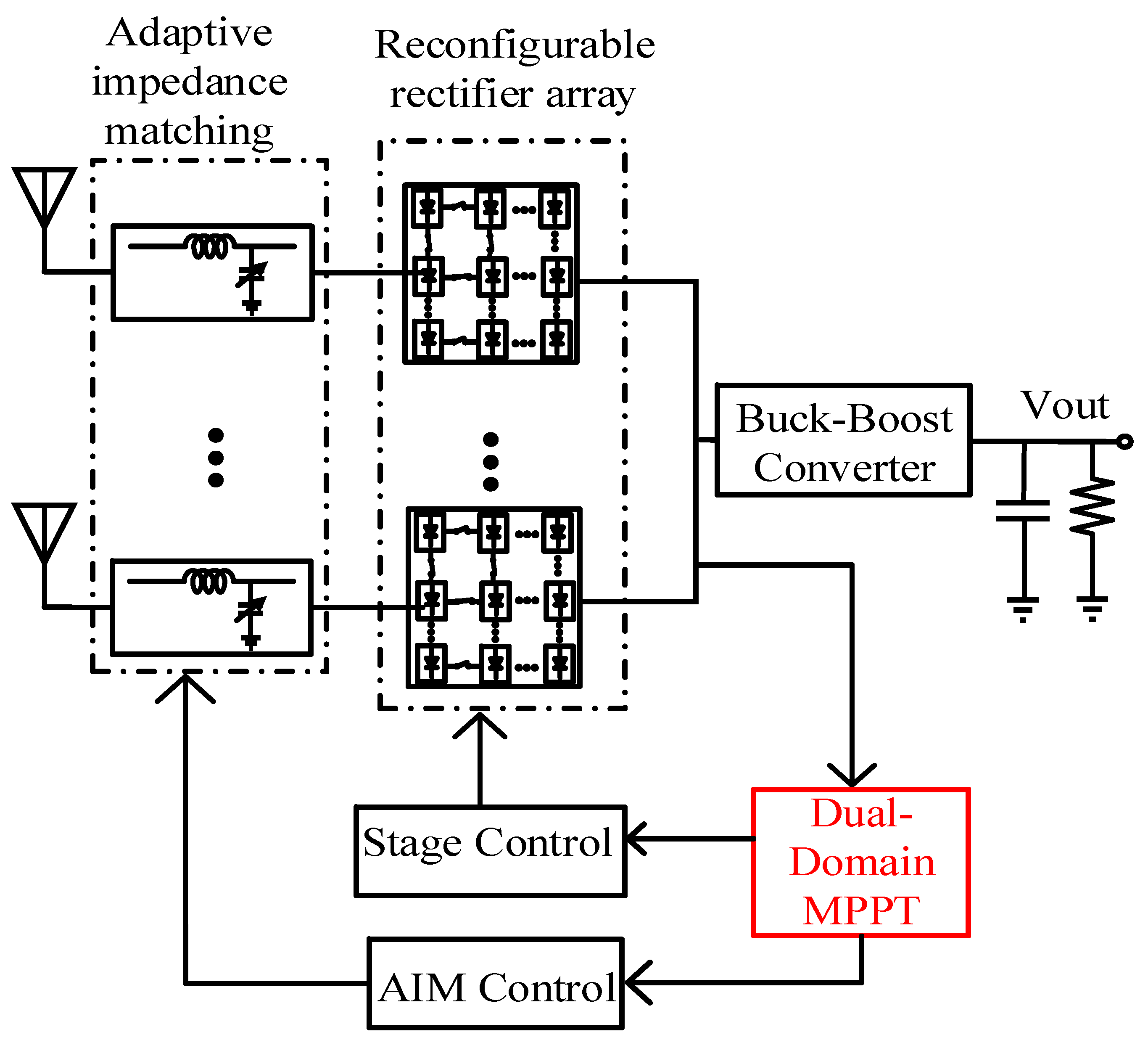
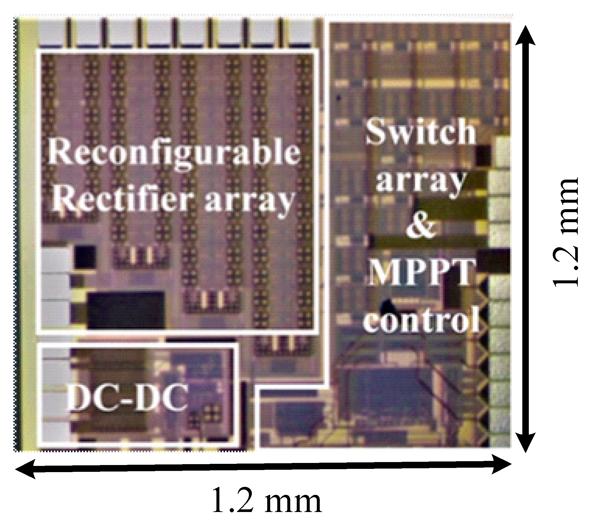
2. System Architecture

As shown in Figure 2, the proposed system consists of 4 groups of reconfigurable rectifier arrays with various stages in each group, the adaptive impedance matching capacitor arrays, the dual-domain maximum power tracking circuits, and a buck-boost converter.
The proposed reconfigurable rectifier array and adaptive impedance matching (AIM) array are controlled by the stage control and the AIM control, respectively. The proposed dual-domain MPPT continuously detects the output voltage of the rectifier array. The perturbation observation method is utilized to find the optimal array configurations. The compensation capacitance will be configured to provide the optimal impedance matching for the current input energy. The cycle time of the proposed maximum power tracking is 22 μs. The output voltage is further regulated to 1 V through a buck-boost converter. In this work, the input RF energy range is from −25 to 5 dBm, and the output loading varies from 20 kΩ to 1 MΩ.

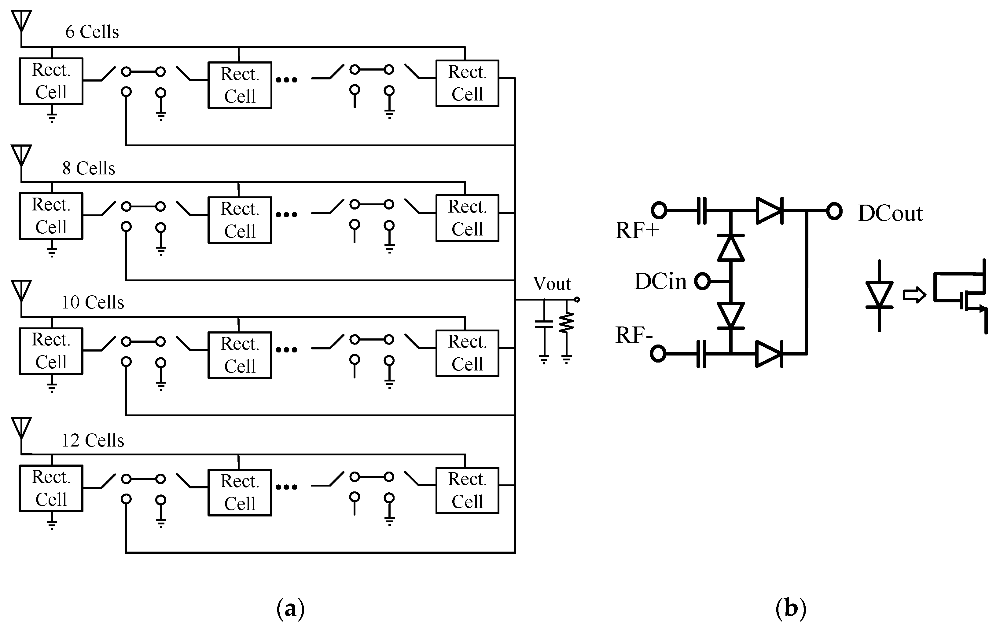
2.1. Multi-Input Reconfigurable Rectifier Array

Although the active rectifiers can provide high power efficiency, it requires a minimum energy supply for the controller, limiting the dynamic range of energy harvesting. As shown in Figure 3a, a differential rectifier composed of 4 diode-connected low-Vth NMOS is used to improve the conversion efficiency and the dynamic range. The performance of conventional Dickson rectifiers is often limited by the high threshold voltages. In this work, low-Vth NMOS transistors are utilized to improve the efficiency. The number of maximum stages in these 4 groups of rectifiers are designed to be 6, 8, 10, and 12, respectively. The DC path of the rectifier array is connected in parallel by the method of DC power combining [25]. In this way, the phase difference between different antennas will not affect the conversion efficiency of the entire system. The differential rectifier cell is composed of 4 diode-connected low-Vth NMOS transistors, as shown in Figure 3b. The possible configurations and the equivalent output impedance of each group are summarized in Table 1. For example, the group of 12 rectifiers could all be connected in series, providing the output impedance of 12 × Rstg, where Rstg is the output impedance of a single-stage rectifier. Additionally, 6 rectifiers could be connected in series to form a sub-group, and then the two sub-groups are connected in parallel, providing the output impedance of 3 × Rstg. To guarantee better matching between two sub-groups, the number of cascaded stages in each sub-group are designed to be equivalent in this work. Therefore, there are only 3 configurations for the groups of 6, 8, and 10 rectifiers, while there are 5 configurations for the group of 12 rectifiers. Each group of arrays can provide various output impedance through these configurations. By paralleling 4 groups of different numbers of arrays, the entire system has more combinations of output impedance to approach the optimal value for maximum power tracking. In addition, to reduce the conduction loss, transmission gates are used as the switches. Taking into account the maximum current of the overall system, the chip area, and the power consumption of the driver, the conduction resistance of the switches is designed to be 30 Ω in this work.

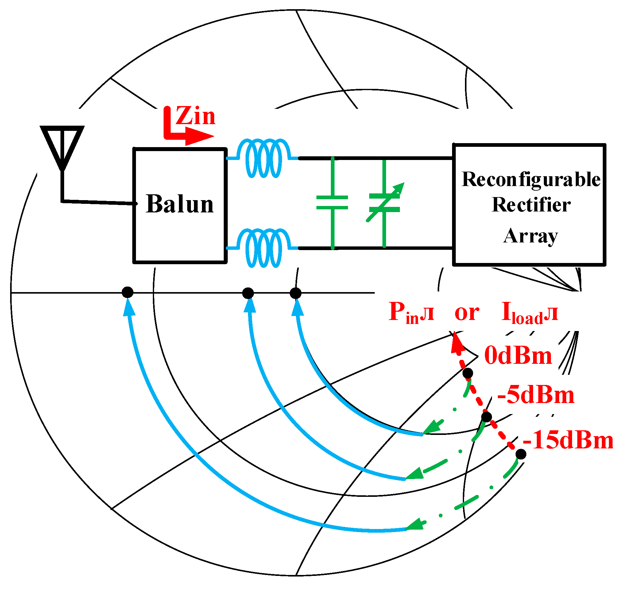
2.2. Adaptive Impedance Matching (AIM) Network

The input impedance of the rectifier changes with the received input energy and complicates the design of the impedance matching network. When the impedance of the antenna and the rectifier do not match to each other, the reflection coefficient becomes large, so the energy collected from the environment fails to completely flow into the rectifier. It causes the input voltage of the rectifier to drop, and the output voltage and the conversion efficiency also decrease. Adding an impedance matching network between the antenna and the rectifier reduces the reflection coefficient. As mentioned above, the reflection coefficient is approximately inverse proportional to the received input energy of the rectifier. We also apply the maximum power tracking in the AC energy domain in this work. The matching network is conventionally designed with a time-consuming recursive process [14]. A simple and efficient process is adopted from [17]. The required parameters of the impedance matching network are designed according to the input energy with a fixed loading. Compared to the recursive method, this process saves much time. Here, the AIM network makes the input impedance of the rectifier match to 50 Ω as much as possible with the feedback of the proposed dual-domain MPPT sensing the input energy, as shown in Figure 4. Figure 5 illustrates the AIM network, composed of a 4-bit binary weighted capacitor array, where Ctotal is 1 pF. To accommodate various ranges of input energy at the rectifier, the capacitor array is made up of two 2 pF capacitors in series. When Qcn = 1, M1, M2, and M3 are on, the drain and source of M2 are connected to ground to reduce its on-resistance, which improves the conversion efficiency.

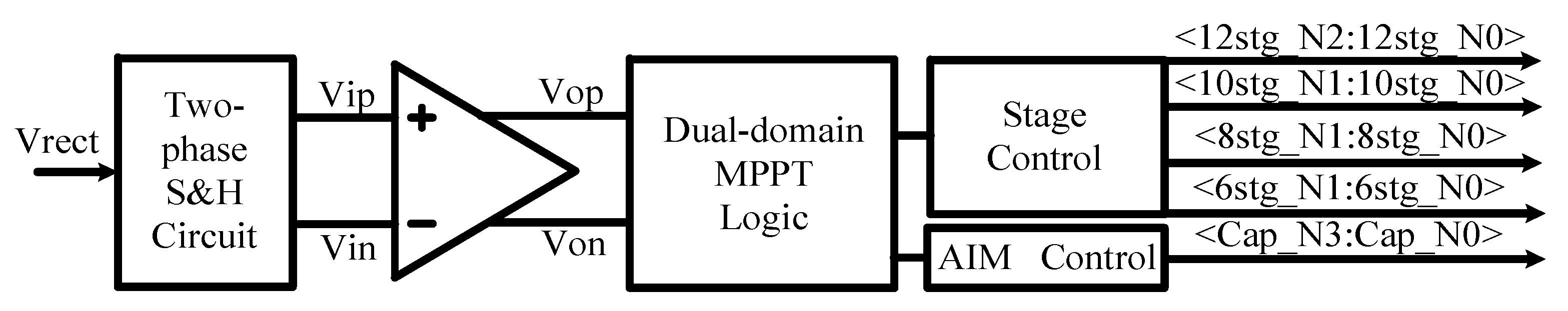
2.3. Dual Domain MPPT

Under the same loading condition and input energy, the configuration that obtains the highest output voltage means that maximum power points have been reached and maximum power is obtained at the output loading. Figure 6 shows the maximum power tracking circuit including a dual-phase sample-and-hold circuit, a comparator, a maximum power tracking logic, a configuration controller, and an AIM controller. The configuration controller signal is designed according to the configuration of the 4 groups of rectifier arrays with a 9-bit control signal. There are 5 configurations for the 12-cell array. The control signal is from 000 to 101. For the 10, 8, and 6-level arrays, there are 3 configurations, and the control signal is 00, 01, and 10. The capacitor array is controlled by a 4-bit thermometer code, 0000 to 1111.
The proposed dual-domain MPPT firstly configures the rectifier (DC-domain MPPT) and then adjusts the impedance matching array (RF-domain MPPT). The algorithm of the maximum power tracking is shown in Figure 7. The perturbation and observation (P&O) method is used to detect Vout of the rectifier to find the maximum power point. If the output voltage with the current configuration is greater than that in the previous configuration, more stages will be connected in series. On the other hand, fewer serial stages will be connected if the output voltage drops. Using the two-phase sample and hold circuit, the sampled voltage will be compared to the held value from the previous sample. At the beginning of MPPT, the 4 rectifier arrays will be initialized to the 2-stage state to avoid possible circuit damages caused by excessively high output voltages. The maximum power tracking in the RF domain starts at the 15th cycle. When performing RF domain MPPT, the control signal of the capacitor array will be reset to 1000 to reduce the time it takes to track the maximum power points. Measurement results show that the proposed dual-domain MPPT takes 22 μs to complete each detection cycle.

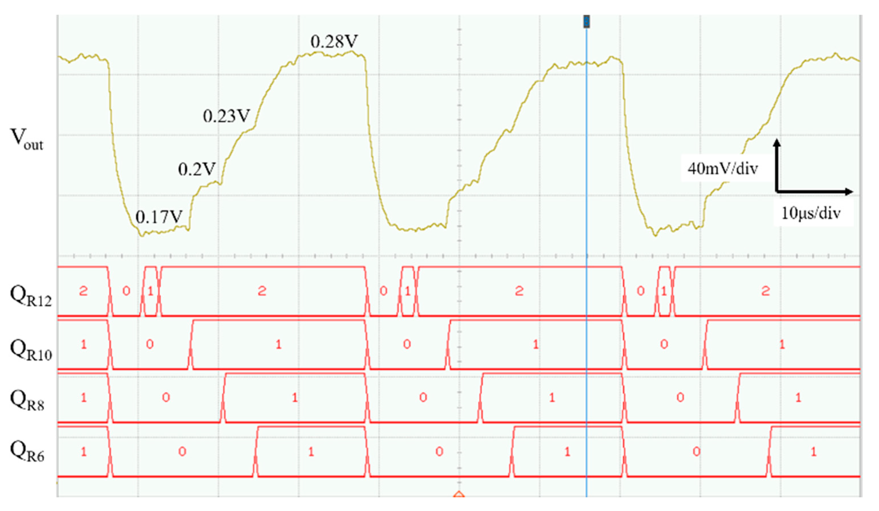
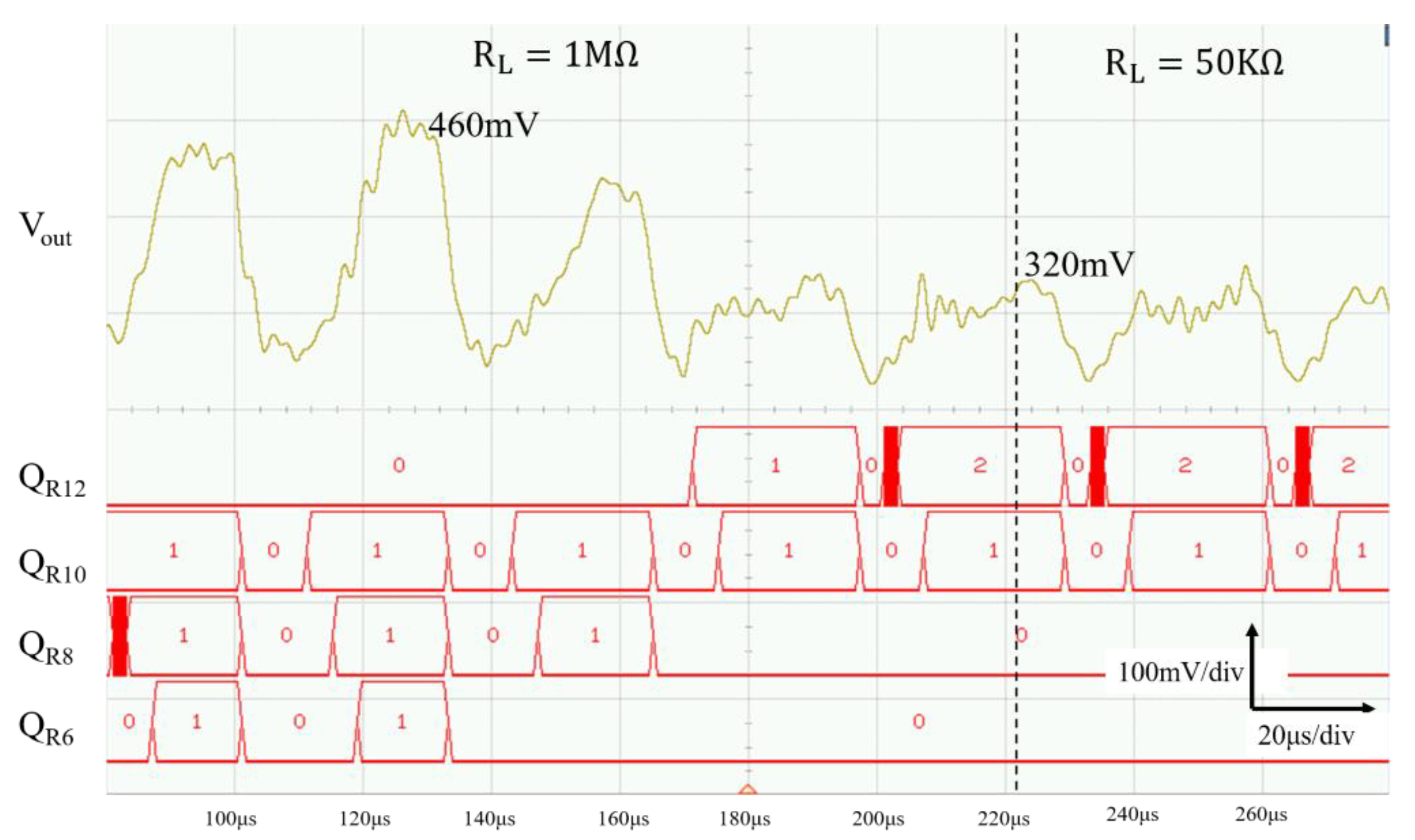
3. Measurement Results

The proposed reconfigurable rectifier array is designed and fabricated in a TSMC 0.18-μm 1P6M process. Figure 8 shows the chip micrograph. The total active area is 1.2 mm × 1.2 mm and KEYSIGHT 81160A is used to emulate the RF signal. Off-chip power dividers and baluns are employed to provide the 4-channel differential inputs.
Figure 9 shows the measurement results of the maximum power tracking process. The input energy is −21 dBm, the output loading is 600 kΩ, and the voltage at the best power point is 0.28 V. The steady-state voltage is 0.28 V. At the beginning of the maximum power tracking, all rectifiers will be reset to a two-stage series connection state. In other words, the control signals for the 4 groups are 000, 00, 00, and 00, respectively. The output voltage drops to 0.17 V when the maximum power tracking starts. The perturbation observation method is used to determine the maximum power points, and it will be maintained until the initialization of the next maximum power tracking cycle. After the configuration of the 6-cell rectifiers is locked, the voltage will fluctuate slightly because the AIM circuit will adjust the compensation capacitance so that the lowest AC energy is reflected at the input of the rectifier.
Figure 10 shows the measured results of Vout in the process of MPPT when the input power is −19 dBm. When the output loading is varied from 1 MΩ to 50 kΩ, Vout varies from 0.46 V to 0.32 V, correspondingly. The control signals, QR12, QR10, QR8, and QR6, in the 12, 10, 8, and 6 stage are 010, 01, 00, and 00, which will configure the number of cascaded rectifiers in the sub-group as 4, 5, 2, and 2, respectively.
Figure 11 illustrates the measured diagram of the input energy versus the output voltage under various loading conditions. The loading resistance ranges from 20 kΩ to 1 MΩ. The larger the loading resistance, the steeper the slope of the output voltage rises with the input energy. The output voltage saturates at about 2.3 V when the input energy is about 0 dBm. When the output loading resistance of 1 MΩ is used, the output voltage of the rectifier reaches 1 V with the input energy of −13.6 dBm. Due to the reconfigurable rectifier array, the output voltage will be adjusted to an appropriate configuration along with the loading conditions to maintain the maximum transmission efficiency. Therefore, the sensitivity of this work is −13.6 dBm.
Figure 12 demonstrates a three-dimensional graph of the input energy versus the measured efficiency with different loading conditions. When the loading resistance is above 500 kΩ, the efficiency is only 5% or less, and the conversion efficiency becomes higher with loading resistance lower than 300 kΩ. The efficiency peaks appear in the input energy ranges of −6 dBm to −9 dBm. Figure 13 shows measurement results of the input energy vs. efficiency with an output loading resistance of 20 kΩ. The maximum conversion efficiency is 49.06% at Pin of −6 dBm. The dynamic range where the conversion efficiency is higher than 20% is 21 dB, from −21 dBm to 0 dBm.
Table 2 summarizes the comparison of our proposed system with the previous works. Comparing with previous works, a 4-channel rectifier array in parallel with asymmetric configuration is employed in this work. It extends the high PCE range to 21 dB, with a peak efficiency of 49.06% at Pin of −6 dBm.

4. Conclusions

The paper proposes a multi-antenna reconfigurable-input rectifier array with dual-domain maximum power tracking. A matching capacitor array and rectifier array are both implemented to be reconfigurable to reach the RF-DC maximum output power. The reflections and RF-DC conversion are both optimized at the same time to improve the overall sensitivity and efficiency. As a result, the range of high conversion efficiency is greatly extended. Measurement results show that maximum PCE is 49.06% and the high PCE range is 21 dB with an input energy of −6 dBm.

Author Contributions

Conceptualization, T.-H.T. and M.-C.C.; validation, M.-C.C., T.-W.S. and T.-H.T.; formal analysis, M.-C.C.; investigation, T.-W.S.; writing—original draft preparation, M.-C.C.; writing—review and editing, T.-W.S. and T.-H.T.; supervision, T.-H.T.; project administration, T.-H.T.; funding acquisition, T.-H.T. All authors have read and agreed to the published version of the manuscript.

Funding

This work was supported by the Ministry of Science and Technology, Taiwan under Grants MOST 109-2221-E-194-034-MY3 and MOST 110-2221-E-194-049-.

Acknowledgments

The authors would like to acknowledge the chip fabrication support provided by the Taiwan Semiconductor Research Institute (TSRI), Taiwan.

Conflicts of Interest

The authors declare no conflict of interest.

References

  1. Hu, Y.-J.; Chen, I.-C.; Tsai, T.-H. A piezoelectric vibration energy harvesting system with improved power extraction capability. In Proceedings of the 2016 IEEE Asian Solid-State Circuits Conference (A-SSCC), Toyama, Japan, 7–9 November 2016; pp. 305–308. [Google Scholar]
  2. Paul, S.; Honkote, V.; Kim, R.G.; Majumder, T.; Aseron, P.A.; Grossnickle, V.; Sankman, R.; Mallik, D.; Wang, T.; Vangal, S.; et al. A Sub-cm3 Energy-Harvesting Stacked Wireless Sensor Node Featuring a Near-Threshold Voltage IA-32 Microcontroller in 14-nm Tri-Gate CMOS for Always-ON Always-Sensing Applications. IEEE J. Solid-State Circuits 2017, 52, 961–971. [Google Scholar] [CrossRef]
  3. Martinez, B.; Montón, M.; Vilajosana, I.; Prades, J.D. The Power of Models: Modeling Power Consumption for IoT Devices. IEEE Sens. J. 2015, 15, 5777–5789. [Google Scholar] [CrossRef] [Green Version]
  4. Scheidl, A.; Pott, P.P. Energy Harvesting in and on the Human Body. In Proceedings of the ACTUATOR; International Conference and Exhibition on New Actuator Systems and Applications, Online Event, 17–19 February 2021. [Google Scholar]
  5. Schmidt, C.L.; Scott, E.R. Energy harvesting and implantable medical devices-first order selection criteria. In Proceedings of the 2011 International Electron Devices Meeting, Washington, DC, USA, 5–7 December 2011. [Google Scholar] [CrossRef]
  6. Bandyopadhyay, S.; Chandrakasan, A.P. Platform Architecture for Solar, Thermal, and Vibration Energy Combining with MPPT and Single Inductor. IEEE J. Solid-State Circuits 2012, 47, 2199–2215. [Google Scholar] [CrossRef]
  7. Shao, H.; Li, X.; Tsui, C.; Ki, W. A Novel Single-Inductor Dual-Input Dual-Output DC–DC Converter with PWM Control for Solar Energy Harvesting System. IEEE Trans. Very Large Scale Integr. (VLSI) Syst. 2014, 22, 1693–1704. [Google Scholar] [CrossRef]
  8. Lu, C.; Raghunathan, V.; Roy, K. Efficient Design of Micro-Scale Energy Harvesting Systems. IEEE J. Emerg. Sel. Top. Circuits Syst. 2011, 1, 254–266. [Google Scholar] [CrossRef]
  9. Raghunathan, V.; Chou, P.H. Design and power management of energy harvesting embedded systems. In Proceedings of the 2006 International Symposium on Low Power Electronics and Design, Tegernsee, Germany, 4–6 October 2006; pp. 369–374. [Google Scholar]
  10. Ruan, T.; Chew, Z.J.; Zhu, M. Energy-Aware Approaches for Energy Harvesting Powered Wireless Sensor Nodes. IEEE Sens. J. 2017, 17, 2165–2173. [Google Scholar] [CrossRef]
  11. Sanislav, T.; Mois, G.D.; Zeadally, S.; Folea, S.C. Energy Harvesting Techniques for Internet of Things (IoT). IEEE Access 2021, 9, 39530–39549. [Google Scholar] [CrossRef]
  12. Garg, N.; Garg, R. Energy harvesting in IoT devices: A survey. In Proceedings of the 2017 International Conference on Intelligent Sustainable Systems (ICISS), Palladam, India, 7–8 December 2017; pp. 127–131. [Google Scholar] [CrossRef]
  13. Panahi, F.H.; Moshirvaziri, S.; Mihemmedi, Y.; Panahi, F.H.; Ohtsuki, T. Smart Energy Harvesting for Internet of Things. In Proceedings of the 2018 Smart Grid Conference (SGC), Sanandaj, Iran, 28–29 November 2018. [Google Scholar] [CrossRef]
  14. Eltresy, N.A.; Dardeer, O.M.; Al-Habal, A.; Elhariri, E.; Hassan, A.H.; Khattab, A.; Elsheakh, D.N.; Taie, S.A.; Mostafa, H.; Elsadek, H.A.; et al. Energy Harvesting IoT System for Museum Ambience Control with Deep Learning. Sensors 2019, 19, 4465. [Google Scholar] [CrossRef] [PubMed] [Green Version]
  15. Colaiuda, D.; Ulisse, I.; Ferri, G. Rectifiers’ Design and Optimization for a Dual-Channel RF Energy Harvester. J. Low Power Electron. Appl. 2020, 10, 11. [Google Scholar] [CrossRef] [Green Version]
  16. Zeng, Z.; Shen, S.; Zhong, X.; Li, X.; Tsui, C.Y. Design of sub-gigahertz reconfigurable RF energy harvester from−22 to 4 dBm with 99.8% peak MPPT power efficiency. IEEE J. Solid-State Circuits 2019, 54, 2601–2613. [Google Scholar] [CrossRef]
  17. Wang, J.; Jiang, Y.; Dijkhuis, J.; Dolmans, G.; Gao, H.; Baltus, P. A 900 MHz RF energy harvesting system in 40 nm CMOS technology with efficiency peaking at 47% and higher than 30% over a 22dB wide input power range. In Proceedings of the 43rd European Solid-State Circuits Conference (ESSCIRC 2017), Leuven, Belgium, 11–14 September 2017. [Google Scholar]
  18. Ballo, A.; Grasso, A.D.; Palumbo, G. A review of charge pump topologies for the power management of IoT nodes. Electronics 2019, 8, 480. [Google Scholar] [CrossRef] [Green Version]
  19. Whittaker, K.; Rizkalla, M.; Ytterdal, T. A Low Power FinFET Charge Pump for Energy Harvesting Applications. In Proceedings of the 2020 IEEE 63rd International Midwest Symposium on Circuits and Systems (MWSCAS), Springfield, MA, USA, 9–12 August 2020; pp. 1048–1051. [Google Scholar] [CrossRef]
  20. Ballo, A.; Grasso, A.D.; Palumbo, G. Charge Pump Improvement for Energy Harvesting Applications by Node Pre-Charging. IEEE Trans. Circuits Syst. II Express Briefs 2020, 67, 3312–3316. [Google Scholar] [CrossRef]
  21. Giuseppe, P.; Carrara, F.; Palmisano, G. A 90-nm CMOS threshold-compensated RF energy harvester. IEEE J. Solid-State Circuits 2011, 46, 1985–1997. [Google Scholar]
  22. Liu, Z.; Hsu, Y.P.; Fahs, B.; Hella, M.M. An RF-DC Converter IC with On-Chip Adaptive Impedance Matching and 30μW Peak Output Power for Health Monitoring Applications. IEEE Trans. Very Large Scale Integr. (VLSI) Syst. 2018, 26, 1565–1574. [Google Scholar] [CrossRef]
  23. Xu, P.; Flandre, D.; Bol, D. Analysis, modeling, and design of a 2.45-GHz RF energy harvester for SWIPT IoT smart sensors. IEEE J. Solid-State Circuits 2019, 54, 2717–2729. [Google Scholar] [CrossRef]
  24. Ouda, M.H.; Khalil, W.; Salama, K.N. Self-biased differential rectifier with enhanced dynamic range for wireless powering. IEEE Trans. Circuits Syst. II Express Briefs 2016, 64, 515–519. [Google Scholar] [CrossRef]
  25. Almansouri, A.S.; Ouda, M.H.; Salama, K.N. A CMOS RF-to-DC power converter with 86% efficiency and−19.2-dBm sensitivity. IEEE Trans. Microw. Theory Tech. 2018, 66, 2409–2415. [Google Scholar] [CrossRef] [Green Version]
  26. Abouzied, M.A.; Ravichandran, K.; Sánchez-Sinencio, E. A fully integrated reconfigurable self-startup RF energy-harvesting system with storage capability. IEEE J. Solid-State Circuits 2016, 52, 704–719. [Google Scholar] [CrossRef]
  27. Lee, D.J.; Lee, S.J.; Hwang, I.J.; Lee, W.S.; Yu, J.W. Hybrid power combining rectenna array for wide incident angle coverage in RF energy transfer. IEEE Trans. Microw. Theory Tech. 2017, 65, 3409–3418. [Google Scholar] [CrossRef]
Figure 1. Environment of Wireless Sensor Node (WSN).
Energies 15 02068 g001
Figure 2. The proposed RF energy harvesting system.
Energies 15 02068 g002
Figure 3. (a) A 4-input reconfigurable rectifier array and (b) single rectifier cell.
Energies 15 02068 g003
Figure 4. The proposed adaptive impedance matching network.
Energies 15 02068 g004
Figure 5. Capacitor array of AIM network.
Energies 15 02068 g005
Figure 6. The MPPT controller.
Energies 15 02068 g006
Figure 7. (a) The MPPT flow chart and (b) two-phase sample and hold circuit.
Energies 15 02068 g007
Figure 8. Chip micro photograph.
Energies 15 02068 g008
Figure 9. MPPT measurement with Pin is −21 dBm and output loading of 600 kΩ.
Energies 15 02068 g009
Figure 10. Measurement output of Vout when Pin is −19 dBm while the loading varied from 1 MΩ to 50 kΩ.
Energies 15 02068 g010
Figure 11. Measurement output of Vout under different loading.
Energies 15 02068 g011
Figure 12. PCE measurement under different loading.
Energies 15 02068 g012
Figure 13. The PCE measurement under 20 kΩ loading.
Energies 15 02068 g013
Table 1. Configuration and Rout of each group.
# of RectifiersConfigurations (# of Stages)Rout
1212-6-4-3-212RSTG ~ RSTG/6
1010-5-210RSTG ~ RSTG/5
88-4-28RSTG ~ RSTG/4
66-3-26RSTG ~ RSTG/3
Table 2. Comparison Table.
ESSCIRC’17 [17]TVLSI’18 [22]JSSC’17 [26]JSSC’19 [16]This Work
Freq. (MHz)900915915915433
Tech. (nm)40130180180180
Input channel11114
Stage number131–2–4–82–3–4–6–126–8–10–12
Vout<2.45 v0.2–2.2>1 v0.4–2.20.2–2.2
System requirementoff chip balun
and inductors
off chip balun
and inductors
looked-up
table
external voltage
source
off chip balun
and inductors
Sensitivity (1V@1M ohm)−15 dBm−12.3 dBm−14.8 dBm−17.8 dBm−13.6 dBm
Matching networkoff chip
and tunable
on chip
and tunable
on chip
and tunable
off chipon chip
and tunable
MPPT durationX0.69 μsalways on60 μs22 μs
Peak efficiency66% @0 dBm19.3% @−4 dBm25% @0 dBm34.4% @1.3 dBm49.06% @−6 dBm
High PCE range (>20%)N/AN/A10 dB13 dB21 dB
Die area (mm2)N/A0.171.080.40.24
RF signal cyclesX631X54,9009526
RF signal cycles = input RF signal × MPPT duration
Publisher’s Note: MDPI stays neutral with regard to jurisdictional claims in published maps and institutional affiliations.

