1. Introduction
Our time is characterised by the wide application of various cyber-physical systems (CPSs) in many areas of human activity [
1,
2,
3,
4,
5,
6]. The typical CPS includes a digital part interacted with physical objects [
7]. Very often, various sequential blocks can be found in digital parts of CPSs [
3,
7]. To improve the overall quality of a CPS digital part, it is necessary to optimize characteristics of its sequential blocks. In the current paper, the model of Mealy finite state machine (FSM) [
8] represents the behaviour of these blocks.
The model of Mealy FSM [
9] is one of the basic models used in the designing circuits of sequential devices [
9,
10]. Due to it, there are a large number of methods for synthesizing Mealy FSM logic circuits [
11,
12]. One of the main goals of these methods is to reach optimal values of the basic characteristics of resulting FSM circuits [
10,
13]. These characteristics are: (1) the hardware amount (in the case of VLSI, it is a chip area occupied by a circuit), (2) the performance, and (3) the power consumption. As a rule, it is not possible to achieve a simultaneous optimum for these three characteristics. For example, a decrease in the occupied chip area is often associated with an increase in the number of circuit levels, which leads to a decrease in performance [
9,
11]. Many studies show that the chip area occupied by an FSM circuit has a decisive influence on both the latency time and power consumption [
14]. At the same time, it is important that reducing the area increases the delay time of the circuit as little as possible. In this paper, we propose just such a method focused on the case of the implementation of the FSM circuit using resources of FPGAs [
5,
15,
16]. The proposed method develops ideas related to the use of extended state codes [
17] and twofold state assignment [
5]. The proposed approach belongs to methods of structural decomposition [
17].
Now, a lot of digital systems are implemented using FPGA chips [
5]. As follows from the analysis of VLSI’ market [
16], the largest manufacturer of FPGA chips is Xilinx [
18]. Due to it, we focus our current research on solutions of Xilinx. An FSM circuit is represented as a composition of look-up table (LUT) elements, programmable flip-flops, inter-slice multiplexers, programmable interconnects, synchronization tree, and programmable input-outputs.
Our current article is devoted to improving the LUT count of two-level LUT-based Mealy FSM circuits based on extended state codes (ESC) [
17]. The main shortcoming of ESC-based FSMs is a significant increase in the number of used flip-flops compared to their minimum possible number. This disadvantage leads to two negative phenomena. First of all, this leads to increasing the number of outputs of the synchronization tree connected with the state code register (SCR). The second negative phenomenon is reduced to the fact that an increase in the state code length (number of bits) leads to a complication of the interconnect system. The negative impact of these two factors is reflected in the increase in power consumption of FSM circuits. This is why it is so important to reduce the number of flip-flops in SCR (without increasing the number of LUT levels of the resulting FSM circuit). The desire to eliminate this shortcoming is the main motivation of our current research. Therefore, the problem under consideration is formulated as follows: the development of a method for implementing circuits of LUT-based Mealy FSMs that allows for the simultaneous reduction of the number of LUTs and flip-flops in a two-level FSM with extended state codes.
The main contribution of this paper is the following:
There is proposed a new method for presenting FSM state codes. The proposed composite state codes (CSCs) consist of class codes and codes of class elements.
The proposed method allows us to obtain FPGA-based circuits having fewer LUTs than this number for circuits of equivalent Mealy FSMs implemented using known basic state encoding approaches (maximum binary, one-hot, JEDI), as well as the extended state codes. A positive side effect of the proposed method is a slight improvement in the temporal characteristics of the obtained FSM circuits in relation to their counterparts based on other state assignment approaches.
The gain from the application of the proposed method increases as the number of FSM inputs and states increases.
The novelty of our article is reduced to the development of a novel design method aimed at reducing the length of state codes for the two-level LUT-based Mealy FSMs. The method is based on using the composite state codes proposed in this paper. This reducing the length of state codes decreases the number of flip-flops in FSM state registers compared to this number for equivalent FSMs with extended state codes. As a result, the number of input memory functions is also reduced, which in turn reduces the LUT counts of the resulting circuits.
The biggest challenge in reducing the LUT counts in the circuits of FPGA-based FSM is to solve this problem with a minimum decrease in FSM performance. We solved this problem by reducing the number of state variables while keeping the same number of logical levels of FSM circuits compared to this value for optimized ESC-based FSMs.
The rest of the article is organized as follows. The basic information about LUT-based Mealy FSMs is discussed in
Section 2. The
Section 3 is devoted to the analysis of works related to FSM design. The background of the proposed method is shown in
Section 4. An example of synthesis for a CSC-based FSM is shown in
Section 5.
Section 6 describes and analyzes the experimental results. The brief summary of the results is shown in
Section 7.
2. Background Information
To design a Mealy FSM logic circuit, it is necessary to create systems of Boolean functions (SBFs) representing the circuit [
8,
9]. These SBFs show the dependences of FSM outputs and input memory functions (IMFs) on FSM inputs and state variables. The FSM outputs form a set
. Elements of the following sets are used as arguments of these SBFs: the FSM inputs from a set
and state variables from a set
. The state variables encode internal states from a set
. In this article, we use a case of maximum binary state encoding [
9] when the number of state variables
is determined as
The state codes
are kept into the state code register. As a rule, the register has informational inputs of D type [
19,
20]. To load state codes into SCR, the input memory functions are used. They form a set
.
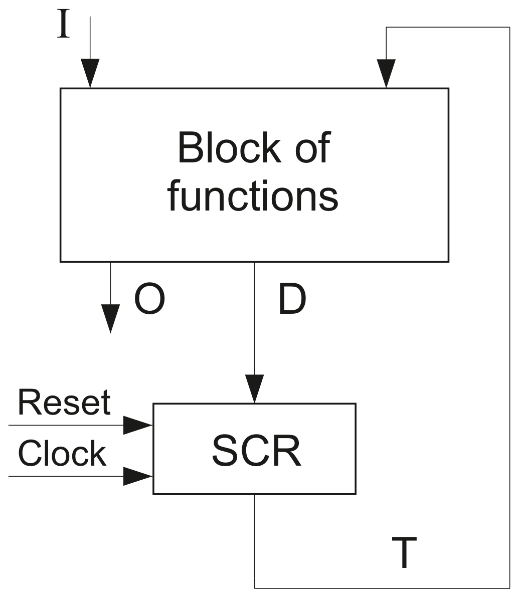
Two systems of functions represent logic circuits of so called P Mealy FSMs (
Figure 1). They are the following:
In
Figure 1, the block of functions is synthesized using the SBFs (
2) and (
3). The SCR consists of
R flip-flops and keeps the state codes
. The pulse
Reset allows us to load the code with all zeros into SCR. As a rule, this combination of state variables encodes an initial state
. The pulse
Clock allows loading state codes into SCR.
To get the systems (
2) and (
3), an FSM direct structure table (DST) is used [
8]. The DST is constructed using either a state transition table (STT) [
9] or a state transition graph [
5,
9]. In our paper, we use an STT as a tool for representing a Mealy FSM.
There are five columns in an STT [
9]. These columns include: a current state
; a next state
; an input signal
which is a conjunction of inputs (or their complements) determining the transition from
into
; collection of outputs
which are produced during the transition from
into
;
h is a column which includes the numbers of interstate transitions
.
The process of a DST creating begins from the executing state assignment. During this step, abstract states
are represented by their binary codes
. Next, a set of input memory functions can be obtained. Compared to an STT, a DST includes three additional columns [
8]. They are: the code
, the code
, and a collection of IMFs
equal to 1 to load the code
into SCR.
In this paper, we consider a case when SBFs (
2) and (
3) are implemented using internal resources of FPGA chips. There are a lot of configurable logic blocks (CLB) in FPGAs produced by Xilinx [
18,
21]. To get an FSM circuit, it is necessary to connect CLBs using internal programmable interconnections [
15]. It is enough three CLB elements to get an FSM circuit. The logic is implemented using LUTs. The expansion of LUT inputs is executed using internal multiplexers. The state register is represented by a collection of D flip-flops. Using the notation [
11], we denote as
-LUT a LUT having
inputs and a single output. A Boolean function depending on up to
variables is represented by a single-LUT logic circuit. Various methods of functional decomposition (FD) [
22,
23] are used if some FSM functions depend on more than
arguments. It is known, the FD-based FSMs are represented by multi-level circuits with complicated systems of “spaghetti-type” interconnections [
22].
If all LUTs have the same number of inputs, then such a logic basis is inflexible. It means that in some cases, only a part of the available inputs will be used. At the same time, in other cases, the LUTs need to be combined to increase the number of inputs. To reduce the impact of interconnects on such a join, it is important to have internal fast interconnects between some LUTs. In Xilinx solutions, these CLBs are combined into slices [
18]. For example, the SLICEL of Virtex-7 includes four 6-LUTs, eight flip-flops and 27 multiplexers [
24]. A part of SLICEL is shown in
Figure 2.
As follows from
Figure 2, using the resources of a single SLICEL allows the generation of up to 11 Boolean functions
–
. The outputs
are outputs of corresponding 6-LUTs. They can be connected with the data inputs of flip-flops. Each 6-LUT can be organized as two 5-LUTs with shared inputs. These 5-LUTs generate functions
–
. An output of each 5-LUT can be connected with informational input of a flip-flop. Due to it, there are 8 flip-flops in the circuit of SLICEL. The slice contains three internal multiplexers (MX1–MX3) which can be used for creating either two 7-LUTs or a single 8-LUT. These multiplexers have special control inputs (MC1–MC3), which can be used as additional inputs of LUTs having
equal to either 7 or 8. For example, using the input MC1, we can get a 7-LUT by combining LUT1 and LUT2. This 7-LUT implements function f9. Simultaneous using MC1–MC3 allows us to combine all 6-LUTs into a single 8-LUT with output f11.
In this paper, we use multiplexers to generate functions (
2) and (
3). We denote a multiplexer having
K data inputs as
K-
. Using a single 6-LUT, we can implement a circuit of 4-
. A 4-
has two control inputs and four data inputs. Using an internal multiplexer, we can organize an 8-
with help of two 6-LUTs. For example, using MC2, LUT3 and LUT4 gives us an 8-
. Its circuit has only slightly bigger delay than a circuit of a 4-
[
24]. It is possible due to using the fast interconnections inside a slice. If a 16-
has the control inputs
–
, then its circuit includes four 6-LUTs controlled by
–
. The inputs MC1 and MC2 are connected with the same control input
. The input MC3 is connected with the most significant control bit
. Obviously, to implement a 32-
, we should use to slices and inter-slice interconnections. Due to it, a 32-
is much slower than a 16-
.
In LUT-based FSMs, the flip-flops of SCR are distributed among LUTs generating functions (
2). Due to it, the SCR is hidden inside the same slices where the input memory functions are generated. There are two blocks in LUT-based
P Mealy FSM (
Figure 3).
The block of state variables (BSV) implements SBF (
2). The state variables
are kept into the distributed SCR. To control the SRC operation, the signals clearing (
Reset) and synchronization (
Clock) enter BSV. The outputs
are generated by the block of output functions (BOF). This block implements SBF (
3).
In the best case, there is exactly a single level of LUTs in the circuit of
P FSM. This is possible if each function
depends on not more than
arguments. However, for modern LUTs, the following relation holds:
[
18,
25]. To diminish the number of LUTs in an FSM logic circuit, it is necessary to increase the value of
. However, such an increasing leads to higher values of both the power consumption and latency time of a LUT. Due to this phenomenon, the number of LUT inputs is so small. If the numbers of arguments in functions
exceed the number of LUT inputs, then it results in increasing the numbers of LUTs and their logic levels in FSM circuits. To improve these characteristics of LUT-based FSM circuits, it is necessary to improve the existing design methods.
In addition, it is necessary to optimize the system of connections between different slices of an FSM circuit. As shown in [
26], the interconnections are responsible for around 70% of power consumption. In addition, they are responsible for the major part of FSM circuit latency time [
23]. As shown [
11], the improving interconnections allows us to decrease the minimum latency time and power dissipation of FPGA-based circuits. Using either twofold state codes [
5] or extended state codes [
17] can improve the interconnection system characteristics.
3. Related Work
Various design methods have been proposed for designing LUT-based FSMs [
5,
19,
20,
23,
27,
28,
29,
30]. These methods should be applied if the number of arguments
exceeds the value of
at least for a single function
[
5]. These methods can improve either the LUT count or the maximum operating frequency or the consumed power [
31]. Sometimes, these methods try to find a solution when more than a single characteristic is optimized. In this paper, we propose a method for improving the LUT count of FPGA-based Mealy FSMs.
To diminish the values of
, various methods of state assignment may be used [
9,
10]. The numbers of state variables differ from (
1) corresponding to maximum binary codes to
M corresponding to the one-hot state assignment. These approaches are used in many academic and industrial CAD tools. The well-known academic systems are, for example, SIS [
13] and ABC by Berkeley [
32,
33]. The manufactures of FPGA chips also have their CAD packages. For example, Xilinx has the CAD Vivado [
34], whereas Intel (Altera) has the package Quartus [
35].
It is very difficult to choose the best universal method of state assignment. For example, in [
36] there are compared FSM circuits based on the maximum binary and one-hot state codes (OHC) [
28]. As follows from [
36], the using OHCs leads to improving the basic characteristics for rather complex FSMs having more than 16 states. However, FSM characteristics depend strongly on the number of inputs, too [
5].The results of research reported in [
28] prove that OHCs lead to the worsening FSM characteristics if there is
.
So, the characteristics of LUT-based circuits depend on the value of
. Depending on this parameter, either the maximum state codes or OHCs lead to improving either the LUT count or/and the latency time for a particular FSM. Therefore, both these state assignment approaches should be checked for a given FSM. We have investigated the efficiency of these both methods in our research. Both these methods are used in the CAD tool Vivado [
34] by Xilinx [
18]. They are named Auto and One-hot, respectively. We used Vivado because this system operates with Virtex-7 chips used in our experiments. It is noted in [
13] that one of the best deterministic methods of the state assignment is JEDI [
28]. Due to this quality, we use JEDI to compare JEDI-based FSMs with FSMs proposed by us in the current paper.
In this paper, we propose a new design method allowing to reduce the number of LUTs (LUT counts) in circuits of FPGA-based Mealy FSMs. The proposed method belongs to the methods of structural decomposition (SD) [
11]. The SD-based FSM optimization is achieved due to using some intermediate logic levels between the arguments of SBFs (
2) and (
3) and the functions
. Due to it, the number of functions increases, but these functions have significantly fewer arguments than functions (
2) and (
3). These methods are analysed, for example, in [
11].
The proposed method can be viewed as an evolution of methods of twofold state assignment [
5]. The methods of this group are based on the constructing a partition
of the set
S by the classes of compatible states. Each state
corresponds to a set
. This set consists of inputs
which determine next states for a given state. Let the symbols
and
stand for the number of states in some set
and the number of bits in maximal binary codes of these states, respectively. In the case of twofold state assignment, it is necessary to use an additional code for the relation
. Therefore, the value of
is determined by the following expression:
We name states
compatible if the following condition holds:
In (
5), the symbol
stands for the number of inputs determining transitions from states
. These inputs are combined into a set
.
In [
5], the method is proposed which allows the creation of the partition
with minimum number of classes,
J. Each class
includes only compatible states. Each class
determines sets
and
. The set
consists of outputs
generating during transitions from states
.
In the case of twofold state assignment, two different codes determine a state
[
5]. To determine this state as an element of the set of states, we use a code
. The code
determines the state
as an element of some class of compatibility
. Each class
determines a collection of partial functions generating by the corresponding block of LUTs. These partial functions are partial outputs
and partial IMFs
. The set
includes IMFs generating during the transitions from the states
. We denote these partial functions as
and
, where the superscript
j shows that the functions are determined by the class
. Due to the validity of (
5), each partial function is represented by a circuit consisting of a single LUT.
The main disadvantage of this approach is the need for a transformation of into . The transformation is executed by a special block of code transformation. This block consumes some internal resources of an FPGA chip. Moreover, it adds a delay to the total cycle time of a resulting FSM circuit.
An improvement of this approach is proposed in [
17]. The improvement is reduced to using only codes
. These codes were named the extended state codes (ESCs). Using ESCs, allows the elimination of the block of code transformation. We use the symbol
to show that a Mealy FSM is based on the extended state codes. To encode states from all classes of compatibility,
state variables are used:
The value of
is determined by (
5). To encode states
, the state variables from a set
are used. There are
elements in the set
T, where
.
The logic circuit of
FSMs is represented by a structural diagram (
Figure 4).
The logic circuits of
FSMs have two logic levels. The first level is a block of partial functions (BFP) represented by
J blocks (Block1–BlockJ). These blocks implements system of partial functions:
The second level of logic is represented by BlockOR. This block includes the SCR having
flip-flops. These flip-flops are controlled by pulses
Reset and
Clock. In the best case, there are exactly
LUTs in the circuit of BlockOR. This block implements disjunctions of the partial functions:
In (
9) and (
10), the superscript determines the number of block generating the particular partial function. The functions (
10) are inputs of flip-flops. The state variables are outputs of these flip-flops.
Obviously, each class determines three sets: , and , where there are elements in the set D. Two first sets are already defined. The set includes input memory functions generating during transitions from states .
Consider a Mealy FSM
represented by its STT (
Table 1). The following characteristics of
follow from
Table 1: the number of states
, the number of inputs
, the number of outputs
, and the number of transitions
. We denote as
that a Mealy FSM
is implemented using the model
. To synthesize the FSM
, it is necessary to find a partition
. The number of classes,
J, depends on the value of
. We discuss a case when a logic circuit of
is synthesized using LUTs with
inputs.
To find the partition
with the minimum number of classes of compatible states, we can use a method proposed in [
5]. Using this method gives the partition
, where
,
, and
. This gives the values
,
and
.
Using (
4) gives
. This determines the sets
,
,
, and
with
. Obviously, using (
1) gives the minimum possible number of state variables
.
If a state
belongs to a class
, then only some state variables
should differ from zero in the extended state code
. At the same time, if
, then
. One of the possible outcomes of such a state assignment is represented by
Table 2. For example, the following ESCs can be found from
Table 2:
,
,
, and so on.
As follows from experiments [
17], this approach allows an increase in performance up to 15.9% compared with equivalent FSMs based on the twofold state assignment. The growth of operating frequency is accompanied by a slight growth in the LUT count (up to 7.7%).
But the approach [
17] has a serious drawback: the number of state variables can exceed significantly the minimum possible number determined by (
1). This leads to increasing the number of flip-flops in SCR. In turn, this increases the number of buffers of the synchronization tree required by a
FSM logic circuit compared with circuits of equivalent FSMs based on the twofold state assignment. In addition, the number of interconnections is increased.
Now we can sum up and perform a qualitative analysis of the discussed issues. The well-known state assignment methods (the maximum binary codes, one-hot codes, JEDI) do not guarantee a decrease in the number of arguments of all Boolean functions representing an FSM logic circuit. The greater the difference between the total number of FSM inputs and state variables, on the one hand, and the number of LUT, the higher the probability of the need to apply the methods of functional decomposition of SBFs (
2) and (
3). In this case, it is expedient to use methods of structural decomposition, which make it possible to obtain FSM circuits with a guaranteed number of logical levels. In addition, these methods allow getting rid of the “spaghetti-type” interconnection system inherent in LUT-based FSM circuits based on functional decomposition. One of the best structural decomposition methods is based on the use of extended state codes. However, this method is associated with a significant increase in the number of state variables in relation to the minimum value determined by (
1). If this shortcoming is eliminated and the main advantages of the extended state codes are preserved, then it is possible to improve the basic characteristics of the FSM circuits (the LUT counts and performance) in comparison with their counterparts based on extended state codes.
In our current paper we propose an approach which allows an improvement of LUT count for circuits of Mealy FSMs based on the partition of the set S by classes of compatible states.
4. Main Idea of the Proposed Method
The proposed method is based on the finding a partition
of the set
S by
classes of compatible states. In this case, states
are encoded by codes
using
state variables where
To encode a class
by a class code
, it is necessary
bits, where
We propose to represent a state
by the code
which we name a composite state code (CSC). This code is the following:
In (
13), the sign “∗” denotes the concatenation of the codes. There are
state variables in the code (
13). The value of
is determined as
To encode the classes, we use the class variables from the set . To encode states as elements of classes , we use the state variables from the set . Together, these sets form a set having elements.
Each class
determines the following three sets:
,
, and
. These sets have been defined before. There is no set
, because the states for each class are encoded using the same state variables
. Each class
determines the following partial functions:
In (
15) and (
16), the following relation holds:
.
To get the functions
and
, it is necessary to execute multiplexing of partial functions. To do it,
multiplexers should be used. The partial functions are used as data inputs of these multiplexers. The selection of a particular partial function is determined by the class variables
. Therefore, the multiplexers generate the following SBFs:
So, SBFs (
15) and (
16) determine a block of partial functions (BPF). The SBF (
17) determines a multiplexer of state variables (MXSV), the SBF (
18) determines a multiplexer of outputs (MXO). Together, the SBFs (
15) and (
18) determine a structural diagram of
Mealy FSM shown in
Figure 5.
There are three logic blocks in
Mealy FSM. Their functions are clear from the previous text. The block of partial functions implements SBFs (
15) and (
16). The multiplexer of state variables (MXSV) implements SBF (
17). Its circuit includes
multiplexers having
control inputs and up to
data inputs. The outputs of these multiplexers are connected with inputs of flip-flops creating the state code register, RSC. To control the RCS, the pulses of clearing and synchronization enter MXSV. There are
flip-flops in the circuit of RSC. There are
N multiplexers in the circuit of
. The selection of a particular partial function
is executed under the control of state variables
.
If
, then there are
variables in the codes of states
, where
The comparison of formulae (
4) and (
19) shows that classes of the partition
can include more elements than classes of the partition
. This is determined by the absence of 1 in the formula (
19).
For example, if there is , then the following partition can be constructed for Mealy FSM : . Therefore, there are classes for FSM instead of for the equivalent FSM . There are the following classes of compatible states in the discussed case: and .
In the common case, the following conditions hold:
In the case of
, we can find that
,
,
,
, and
. Therefore, in the discussed case, there is
. In addition, there is
. Due to it, we can expect that, in this case, the circuit of
will have fewer LUTs and interconnections than the circuit of
. We will check this in the next Section. In addition, we can expect that
Mealy FSMs have, at least, the same performance as equivalent
Mealy FSMs. The experiments reported in
Section 6 show that our approach allows an improvement of the basic characteristics of LUT-based circuits of Mealy FSMs.
A method of Mealy FSMs logic synthesis is proposed in our current article. As a result, we have obtained the logic circuits of LUT-based FSMs where a LUT has inputs. We start the synthesis process from an FSM state transition table. The proposed method includes the following steps:
Constructing the partition of the set of states by classes of compatible states.
Encoding of FSM states by composite state codes .
Creating direct structure table of Mealy FSM.
Creating tables of blocks of partial functions for classes .
Creating table representing the multiplexer of outputs.
Creating table representing the multiplexer of state variables.
Constructing SBFs representing BPF, MXSV, and MXO.
Implementing the LUT-based circuit of Mealy FSM using FPGA chip’s internal resources.
We use the methods [
5] to create the partition
. The main goal of these methods is the minimizing LUT counts in the resulting Mealy FSM circuits. If it is possible, each class of compatible states should include the maximum possible number of states. This helps minimizing the value of
. The classes are created in a way minimizing the number of shared outputs. This optimizes the number of LUTs in the circuit of MXO. Any multiplexer from the second level of an FSM circuit is implemented by a single LUT if the following condition takes place:
Even if condition (
22) is violated, then the multiplexers could be implemented as single-level circuits. This is possible, if the number of partial functions for a given function
does not exceed the value
.
5. Example of Synthesis
We use the symbol
to show that the model of
Mealy FSM (
Figure 5) is used to implement the circuit of an FSM
. In this Section, we show how to design the circuit of Mealy FSM
using 5-LUTs. The synthesis process starts from
Table 1.
Step 1. In the previous section, using
Table 1 and 5-LUTs, we have got the partition
. The partition includes the classes
and
. Therefore, each class includes four states
. These classes determines the sets
,
,
, and
. Therefore, there is
. Using (
19) gives
. There is
. This means that condition (
5) holds for given FSM and K-LUTs. Therefore, it is possible to use the model
. The total number of elements in the sets
determines how many LUTs are necessary to generated the partial output functions.
The sets and have no shared inputs . This relation shows that there is the optimal system of interconnections between FSM inputs and LUTs of BPF.
Step 2. As we have found, there is
. Using (
14) gives
. Now, we have the sets
,
, and
. One of the possible outcomes of the encoding is shown in
Figure 6.
So, the classes are encoded in the following way: and . For example, the following relation holds: . Using the codes of classes of compatible states gives the following composite state codes: and . Using the same approach, we can find the CSCs for all states .
Step 3. Compared to STT (
Table 1), the DST includes three additional columns. They are:
including a CSC of the current state
;
with a CSC of the state of transition
;
with IMFs equal to 1 to load the code
into SCR. In the discussed example, DST is represented by
Table 3.
Step 4. The DST (
Table 3) determines contents of tables of blocks of partial functions BPF
. In these tables, the column
is replaced by the column
; the column
is replaced by the column
; the column
is replaced by the column
. The superscript
j indicates that these functions are generated by the block BPF
.
In the discussed case, there are two blocks of partial functions.
Table 4 represents the block
and
Table 5 represents the block
. There are
rows in
Table 4, and
rows in
Table 5. Together, these tables have exactly
rows (as the number of rows in
Table 3).
Step 5. There are the following columns in the table of MXO:
,
. The second column is divided by
sub-columns. If a partial output
presents in the table of BPF
, then there is 1 on the intersection of the column
j and the row
. Otherwise, this intersection is marked by 0. The table is constructing using tables of blocks BPF
. In the discussed case, this is
Table 6.
Step 6. There are the following columns in the table of MXSV:
,
. As in the previous case, the column
is divided by
sub-columns. If a partial IMF
presents in the table of BPF
, then there is 1 on the intersection of the column j and the row
. Otherwise, this intersection is marked by 0. The table is constructing using tables of blocks BPF
. In the discussed case, this is
Table 7.
Step 7. The BPF is represented by SBFs (
15) and (
16). These systems are constructed using tables of BPF
. The partial functions depend on product terms which are conjunctions of
and
. The conjunction
is determined by the code
. For example, there is
.
For example, using
Table 4 gives us the following sum-of-products for functions
and
:
Using
Table 5 gives us the following sum-of-products for functions
and
:
Using
Table 6 gives the SBF representing the MXO. This SBF is created in the trivial way. In the discussed case, this is the following system:
Using
Table 7 gives the SBF representing the MXSV. This SBF is created in the trivial way, too. In the discussed case, this is the following system:
Step 8. Using the obtained SBFs, we can get a logic circuit of Mealy FSM
. It is shown in
Figure 7.
Because each partial function includes no more than
arguments, there are 6 LUTs implementing the partial IMFs
and 10 LUTs implementing the partial outputs
. Therefore, there are 16 LUTs in the circuit of BPF. To implement IMFs (
17), it is enough
LUTs. There are 7 LUTs in the circuit of MXO. Therefore, there are 26 5-LUTs in the logic circuit of Mealy FSM
. These LUTs are connected using three buses. The
combines wires with inputs
and state variables
. The
includes wires with partial IMFs
, partial outputs
, and state variables
used as control inputs of multiplexers
MXO and
MXSV. The
BusT is an output bus of the distributed SCR. This bus includes wires with state variables
. The buffers of the synchronization tree control the flip-flops connected with outputs of LUT17-LUT19.
We can compare LUT counts for Mealy FSMs and . In both cases, we use 5-LUTs. We have synthesized the logic circuit of . There is for . There are 10 LUTs in the circuit of Block1, 11 elements in Block2, and 4 elements in Block3. These three blocks represent the block of partial functions having 25 5-LUTs. There are 10 LUTs in the circuit of BlockOR. Therefore, there are 35 5-LUTs in the logic circuit of Mealy FSM . It means that using the model instead of allows a decrease in the LUT count by 35:26 = 1.35 times. At the same time, both circuits have the same number of logic levels.
To get the electrical circuit of Mealy FSMs
, it is necessary to execute the step of technology mapping [
36]. This is connected with using the sophisticated CAD tools. In the case of circuits implemented with internal resources of Virtex-7, the industrial package Vivado [
34] should be used. The Vivado executes the steps of technology mapping (such as mapping, placement, and so on). Obtaining an FSM circuit allows the determination of its real characteristics such as the number of LUTs and the minimum latency time. Using the latency time gives the maximum value of synchronization frequency. In addition, the value of power consumption is determined for the maximum operating frequency.
From the discussion of SLICEL follows that we cannot use Vivado to get the 5-LUT-based circuit of Mealy FSMs
. However, in
Section 6, we show results of experiments conducted using Vivado and the library of benchmark FSMs [
19].
6. Experimental Results
We conducted a lot of experiments to compare the basic characteristics of
-based Mealy FSMs with characteristics of FSM circuits based on some other models. The benchmark FSMs from the library [
37] are used for the experiments. De facto, the used 48 benchmarks are represented by their state transition tables. The tables are represented by KISS2-based files. The basic characteristics of benchmarks (the values of parameters
M,
L, and
N) have a wide range. Due to it, these benchmarks are used in many research as a base for comparison different FSM design methods. We do not show the characteristics of benchmark FSMs in this article. They can be found, for example, in [
17]
We execute the experiments using a personal computer with the following characteristics: CPU: Intel Core i7 6700 K 4.2@4.4 GHz, Memory: 16 GB RAM 2400 MHz CL15. In addition, we use the Virtex-7 VC709 Evaluation Platform (this platform is based on the following FPGA chip: xc7vx690tffg1761-2) [
38] and CAD tool Vivado v2019.1 (64-bit) [
34]. There is
for FPGAs of Virtex-7. We use reports of Vivado to get the results of experiments. To enter Vivado, we use the CAD tool K2F [
5]. This tool allows the creation of VHDL codes on the base of files represented in the KISS2 format.
Three parameters have been compared on the base of our experiments, namely, the chip areas occupied by FSM circuits, performance, and area-time products. To estimate the area, we use the LUT counts taken from reports of Vivado. The performance is represented by the latency time which is achievable for each benchmark FSM. The latency time is shown in Vivado reports. The amount of latency time is inversely proportional to the value of the maximum operating frequency. Thus, the shorter the latency time, the higher the frequency of synchronization pulses can be. The area-time products are calculated as results of multiplication of the LUT counts by the latency times. In our experiments, we use five FSM models. These models are P-FSMs based on either state codes with the minimum length (Auto) or OHCs with maximum number of state variables (One-hot) or some intermediate number of state variables (JEDI). The first two methods are the internal methods of Vivado. Because we try to improve the characteristics of -based FSMs, we use this model in our research. Obviously, we use the model of -based FSMs proposed in the current paper.
As in our previous research [
17], we use the relation between the values of
and
to divide the benchmarks [
37] by 5 categories. For LUTs of Virtex-7, there is
. We use this value to divide the benchmarks by the categories. The FSMs are trivial (category 0), if the result of summation of R and L does not exceeds 6. The FSMs are simple (category 1), if the result of summation does not exceeds 12. The FSMs are average (category 2), if the result of summation does not exceeds 18. The FSMs are big (category 3), if the result of summation does not exceeds 24. Otherwise, the benchmarks FSMs are very big (category 4). It is shown in the article [
5] that there is a direct dependence between the improving of FSM characteristics due to using SD-based methods and the category number.
For our conditions, there is the following distribution of benchmarks [
37] by categories. The category 0 consists of FSMs represented by:
bbtas, dk17, dk27, dk512, ex3, ex5, lion, lion9, mc, modulo12, and
shiftreg. The following FSMs create the category 1:
bbara, bbsse, beecount, cse, dk14, dk15, dk16, donfile, ex2, ex4, ex6, ex7, keyb, mark1, opus, s27, s386, s840, and
sse. The category 2 contains the FSMs:
ex1, kirkman, planet, planet1, pma, s1, s1488, s1494, s1a, s208, styr, and
tma. There is single FSM
sand in the category of big benchmarks. Four FSMs (
s420, s510, s820, and
s832) belong to the category 4.
The results of experiments are shown in
Table 8,
Table 9,
Table 10,
Table 11,
Table 12,
Table 13,
Table 14,
Table 15,
Table 16,
Table 17,
Table 18,
Table 19,
Table 20,
Table 21,
Table 22 and
Table 23. These tables are organized in the same manner. The table columns are marked by the names of investigated methods. The names of benchmarks are written in the table rows. The rows “Total” contain results of summation of values for each column. The row “Percentage” includes the percentage of summarized characteristics of FSM circuits produced by other methods respectively to
-based FSMs. We use the model of
P Mealy FSM as a starting point for methods Auto, One-hot, and JEDI.
Let us analyse the experimental results taken from the tables. The following information can be found in these tables: (1) the LUT counts for all benchmarks (
Table 8); (2) the LUT counts for benchmarks of category 0 (
Table 9); (3) the LUT counts for benchmarks of category 1 (
Table 10); (4) the LUT counts for benchmarks of categories 2–4 (
Table 11); (5) the latency time for all benchmarks (
Table 12); (6) the latency time for benchmarks of category 0 (
Table 13); (7) the latency time for benchmarks of category 1 (
Table 14); (8) the latency time for benchmarks of categories 2–4 (
Table 15); (9) the maximum operating frequency for all benchmarks (
Table 16); (10) the maximum operating frequency for benchmarks of category 0 (
Table 17); (11) the maximum operating frequency for benchmarks of category 1 (
Table 18); (12) the maximum operating frequency for benchmarks of categories 2–4 (
Table 19); (13) the area-time products for all benchmarks (
Table 20); (14) the area-time products for benchmarks of category 0 (
Table 21); (15) the area-time products for benchmarks of category 1 (
Table 22); (16) the area-time products for benchmarks of categories 2–4 (
Table 23).
As follows from
Table 8, the
-based FSMs require fewer LUTs than it is for other investigated methods. Our approach produces circuits having 44.87% less 6-LUTs that it is for equivalent Auto-based FSMs; 68.59% less 6-LUTs that it is for equivalent One-hot-based FSMs; 19.31% less 6-LUTs that it is for equivalent JEDI-based FSMs. While developing our method, we hoped that
-based FSMs will require fewer LUTs in comparison with equivalent
-based FSMs. As follows from the last column of
Table 8, our assumptions turn out to be correct. Our approach produces circuits having an average 15.46% less 6-LUTs that it is for equivalent
-based FSMs.
As follows from
Table 9, our approach loses compared to both Auto-based FSMs (6.04% loss) and JEDI-based FSMs (7.58% loss). However,
Table 9 reflects results for the simplest FSM (category 0). Let us point out that, even in this case, our approach gives a gain compared to One-hot-based (30.3%) and
-based (7.58%) FSMs.
Analysis of
Table 10 and
Table 11 shows that the
-based FSMs have circuits with fewer LUTs compared with all other investigated approaches. Compared with Auto-based FSMs, there is either 33.99% win rate (category 1) or 52.45% of gain (categories 2–4). Compared with One-hot-based FSMs, there is either 73.27% win rate (category 1) or 69.85% of gain (categories 2–4). Compared with JEDI-based FSMs, there is either 11.22% of gain (category 1) or 24.12% win rate (categories 2–4). Compared with
-based FSMs, there is either 12.87% of gain (category 1) or 16.95% win rate (categories 2–4). Therefore, the gain from applying the proposed approach in relation to
-based FSMs increases as the complexity of the FSM increases (increasing the category number).
As follows from
Table 12, our approach produces faster LUT-based FSM circuits relative to other investigated methods. The average win is from 3.01% (compared with
-based FSMs) to 17.71% relative to One-hot based FSMs.
For category 0 (
Table 13), our approach provides minimal gain relative to Auto-based FSMs (0.19%) and One-hot-based FSMs (3.11%). At the same time,
-based FSMs are a bit slower than their counterparts based on either JEDI (0.49%) or extended state codes (0.01%). Of course, such a loss is extremely insignificant. Analysis of
Table 14 and
Table 15 shows that our approach gives gain relatively to all other design methods starting from category 1. For category 1 (
Table 14), there is the following gain in FSM performance: 16.25% compared with Auto, 16.13% compared with One-hot, 8.03% compared with JEDI-based FSMs, and 3.14% compared with
-based counterparts. The gain is increased with increasing the category. This follows from
Table 15 containing experimental results for categories 2–4. For these categories, there is the following gain: (1) 26.03% regarding Auto; (2) 27.12% regarding One-hot; (3) 16.32% regarding JEDI-based FSMs and (4) 4.52% regarding
-based FSMs.
Obviously, using the latency time we can obtain the values of maximum operating frequency. This characteristic for all benchmarks is shown in
Table 16. As follows from
Table 16, our approach produces faster LUT-based FSM circuits relative to other investigated methods. The average win is from 3.99% (compared with
-based FSMs) to 29.04% relative to One-hot based FSMs.
For category 0 (
Table 17), our approach provides minimal gain relative to Auto-based FSMs (0.05%) and One-hot- based FSMs (2.5%). At the same time,
-based FSMs are a bit slower than their counterparts based on either JEDI (0.85%) or extended state codes (0.01%). Of course, such a loss is extremely insignificant. Analysis of
Table 18 and
Table 19 shows that our approach gives gain relatively to all other design methods staring from category 1. For category 1 (
Table 18), there is the following gain in FSM performance: 27.6% compared with Auto, 27.7% compared with One-hot, 22.46% compared with JEDI-based FSMs, and 3.88% compared with
-based counterparts. The gain is increased with increasing the category. Therefore, for categories 2-4 (
Table 19), we have the following gain: (1) 43.61% regarding Auto; (2) 43.76% regarding One-hot; (3) 36.17% regarding JEDI-based FSMs and (4) 6.11% regarding
-based FSMs.
The main goal of our method was to reduce the number of LUTs (the chip area occupied by FSM circuit) compared to
-based FSMs. The results of experiments show that this goal has been achieved. In addition, our approach simultaneously allows an increase in the maximum operating frequency (it is the same as the decreasing of the latency time). Due to it, our approach produces FSM circuits with the best values of area-time products. The corresponding values are shown in
Table 20. Our approach provides the following average gain: (1) 83.10% regarding Auto; (2) 112.15% regarding One-hot; (3) 36.8% regarding JEDI and (4) 20.26% regarding
-based FSMs. Analysis of
Table 21 and
Table 23 shows that the gain obtained by our approach increases with the increasing the FSM category.
For category 0 (
Table 21), our approach loses out to the other two approaches: 4.54% lost relative to Auto-based FSMs and 6.68% lost relative to JEDI-based FSMs. However, for this category, our approach has gain compared with One-hot (35.95%) and
-based FSMs (6.99%).
As follows from
Table 22, our approach provides the win rate equal to: (1) 59.86% regarding Auto; (2) 105.58% regarding one-hot; (3) 21.59% regarding JEDI; (4) 16.53% regarding
-based FSMs. As follows from
Table 23, our approach provides the win rate equal to: (1) 95.58% regarding Auto; (2) 118.97% regarding one-hot; (3) 44.08% regarding JEDI; (4) 22.22% regarding
-based FSMs.
So, the results of our experiments show that the proposed approach can be used instead of other models starting from simple FSMs (category 1). Our approach allows an improvement in LUT counts, maximum operating frequency (minimum latency time), and area-time products compared with other investigated design methods. We think that our approach has rather good potential and can be used in CAD systems targeting FPGA-based Mealy FSMs.


