Article

Simultaneous Lightwave and Power Transfer for Internet of Things Devices

by
José Ilton De Oliveira Filho
,
Omar Alkhazragi
,
Abderrahmen Trichili
*,
Boon S. Ooi
,
Mohamed-Slim Alouini
and
Khaled Nabil Salama
Computer, Electrical and Mathematical Sciences & Engineering, King Abdullah University of Science and Technology, Thuwal 23955, Saudi Arabia
*
Author to whom correspondence should be addressed.
Energies 2022, 15(8), 2814; https://doi.org/10.3390/en15082814
Submission received: 15 February 2022 / Revised: 17 March 2022 / Accepted: 19 March 2022 / Published: 12 April 2022
(This article belongs to the Special Issue Energy Harvesting Circuits and Systems for Low-Power IoT Devices)

Abstract

:
A laudable goal toward achieving autonomous internet of things (IoT) devices would be to use the same circuitry for communication and harvesting energy. One way to achieve it is through simultaneous lightwave and power transfer (SLIPT) that consists of using solar cells to harvest energy and receive information signals. Here, a SLIPT-based system that uses a large area solar panel to harvest energy from light sources and decode data signals is designed. The designed system is equipped with an infrared sensor used to detect the movements of an unmanned aerial vehicle. We equally discuss the wide-scale deployment of IoT devices with SLIPT capability.

1. Introduction

Simultaneous lightwave and information transfer (SLIPT) has seen tremendous progress over the last few years. SLIPT is the optical equivalent of the widely studied simultaneous wireless information and power transfer (SWIPT) using radio frequency (RF) signals used for communication to harvest energy [1,2]. SWIPT can be subject to low conversion efficiency and complicated system design. Compared to SWIPT, SLIPT also has fewer challenges in terms of licensing and allowable electromagnetic field radiation, restricted by maximum RF exposure [3]. SLIPT can co-exist with optical wireless communication (OWC) in the visible and infrared bands, better known as visible light communication (VLC) and free space optics (FSO). Several demonstrations reported in the literature have shown the feasibility of SLIPT in indoor and outdoor media. SLIPT is also useful for underwater wireless optical communication (UWOC) applications.
A seminal paper by Kim and Won reported the reception of 3-kbps signals emitted by a light-emitting diode (LED) using a solar cell (SC) placed 40 cm from the transmitter while harvesting solar energy [4]. Authors of [5] proposed the design of a silicon (Si) SC-based receiver that was able to decode signals modulated using an orthogonal frequency-division multiplexing (OFDM) scheme at a data rate of 11.84 Mbps. The authors also reported receiving optical signals with an amplitude of 0.7 × 10 3 W/cm 2 [5]. An 8-mm 2 organic SC was used to establish a 34.2-Mbps OFDM-based communication link while generating a 0.2-mW power [6]. A 500-Mbps data rate was achieved over a 2-m free space OFDM-based link using a circular Gallium Arsenide (GaAs) SC illuminated by a near-infrared beam emitted by an 847-nm laser [7]. The used GaAs SC has a diameter of 1 mm and a 3-dB bandwidth of 24.5 MHz. A follow-up study using the same SC reported a data rate of 743 Mbps and harvested 1.3 mW of power [8]. A 1-Gbps record data rate was achieved in [9] using the same 0.8-mm 2 GaAs SC used in [7,8]. In addition to the small active area of the SC, a key element for reaching such data rates in [8,9] was the use of an alternating current-direct current (AC-DC) decoupling receiver initially used in [5]. A perovskite SC was used to achieve a 56-Mbps data rate and 20% power conversion under white light LED illumination [10].
We previously proposed the design of a low-cost internet of underwater things (IoUT) device that can harvest energy and received information using a silicon SC. The designed IoUT device contained a temperature sensor and a camera used to stream a video with an integrated laser diode [11]. The potential of SLIPT in underwater media was further highlighted in [12].
Additionally to VLC and UWOC systems, the concept of simultaneous information decoding (ID) and energy harvesting (EH) is seen as a potential solution to coping with the connectivity divide affecting those rural places with low Internet penetration by using already existing photovoltaic panels to receive optical signals while also harvesting solar energy [13,14]. Indeed, a real-world demonstration reported the detection of signals emitted from a distance of 30 m at a data rate of 8 Mbps using a commercially available solar panel that could also harvest 5 W of power from sunlight [14]. We recently demonstrated a self-powered weather station for rural areas and difficult access locations [15]. The designed system was able to decode OOK-modulated data signals received by the SC. The system operated autonomously without any user intervention over a period of one week [15].
In this work, we present a SLIPT-based prototype used to harvest energy from various sources and decode OFDM-modulated signals with different data rates received by a large-area silicon SC. A net data rate of 1.3 Mbps is demonstrated. The designed self-powered device is connected to an IR motion sensor, which is tested to detect the movements of unmanned aerial vehicles (UAVs).

2. Background

SLIPT-based systems can be installed in locations where changing batteries or providing continuous powering is expensive or not possible. An illustration of a generic network of self-powered devices is shown in Figure 1. In a SLIPT-based system, solar panels can operate at any given moment in one of two modes: photovoltaic or photoconductive mode. The photovoltaic mode is the energy harvesting mode, while the photoconductive corresponds to the information signal decoding mode. There are three possible SLIPT configurations: time switching, power splitting, and space switching. In Table 1, we offer a comparison between the different SLIPT methods. The methods are compared in terms of hardware complexity, whether EH and ID are performed simultaneously on time, whether it is possible to perform maximum power point tracking (MPPT) [16] or not, and cost. We recall that time switching consists of using the same receiver to decode data signals and harvest energy over two different time slots. The power splitting approach aims to split an incoming beam using a power splitter into two quantities, one for ID and a second for EH. The complexity of this approach lies mainly in the design of the power splitting component. One device can harvest energy from multiple light sources and receive information signals from at least one transmitter within the space splitting approach. It is not possible to use an MPPT only for the case of power splitting.
The solar panel circuit model for energy harvesting is illustrated in Figure 2a. In the DC model, the photocurrent generation phenomenon can be substituted by a current source I P H . The non-linear relationship between the voltage and the current of the SC can be modeled by a diode, D, that is connected in parallel to the photocurrent source. The leakage current can be expressed as an internal resistance in parallel, R S H , and the internal voltage drop by the cell interconnections can be represented as a series resistor R S [17]. The load, which can be a supercapacitor or a battery, is represented as a pure restive load R L .
The output current I S is the following:
I S = I P H I D I S H ,
where I D and I S H are the currents through the parallel diode and the shunt resistance, respectively [5]. I D can be expressed as follows [5]:
I D = I 0 ( e V S H n V T 1 ) ,
where n is the diode ideality factor and V T is the thermal voltage. In high frequency, the parasitic capacitances of the solar cell start to affect its output; due to this, a capacitor C must be inserted in parallel with the resistor R S H . The diode in AC can be substituted by its small-signal corresponding resistor r once it is considered that the AC component of the light signal has a minor variation compared to the magnitude of the DC component. Figure 2b shows the AC signal representation of an SC in which i P H ( w ) is the photocurrent of the AC signal.
Here, we mainly focus on time switching SLIPT. Our switching circuit has two modes when EH mode is active; the circuit can be modeled as a small resistance R S W , in series with an inductor L S W , that represent the wire connection from the switch to the load Z 1 . When ID is active, the switching circuit is disconnected from the load. The equivalent circuit model of the solar panel in a time switching scenario is given in Figure 3.
If we express Z 1 as a capacitor C 0 followed by a resistor R C , the frequency response of the circuit is given by:
v ( ω ) i P H ( ω ) 2 = R C R S + j ω L S C + R S W + j ω L S W + 1 j ω C 0 + R C 1 r + 1 1 j ω C + 1 R S H + 1 R S + j ω L S C + R S W + j ω L S W + 1 j ω C 0 + R C 2 .

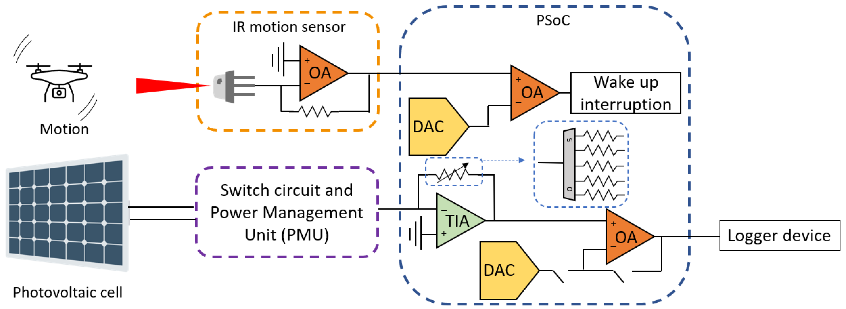
3. System Design and Experimental Methodology

The circuit of the designed system is shown in Figure 4. In addition to a 38.5-cm 2 mono-crystalline Si solar panel (SP), the system is composed of 3 main blocks: an IR motion sensor, switch circuit and power management unit (PMU), and a programmable system on chip (PSOC). The IR motion sensor is used only when the PSoC is in sleep mode and is responsible for triggering a waking-up interruption call when a movement happens. The switch circuit and the PMU are used to interface the SP, enabling the switching of the SP to the photovoltaic mode or photoconductive mode. In the photovoltaic mode, the SP is connected to a PMU that harvests the power and stores it in a battery or supercapacitor. In the present system, we use an EATON 470-mF supercapacitor. An MPPT is included in the PMU to achieve the best response from the SP when harvesting energy. In photoconductive mode, the SP, having a 3-dB bandwidth of 100 kHz, is reverse-polarized and is connected to a transimpedance amplifier (TIA) through the PSoC. If the signal to be received by the SP is analog modulation, a follower is connected internally in the PSoC, serving as a buffer for the Logger device (an oscilloscope or an ESP32 system). If the signal is modulated using an on-off keying (OOK) scheme, the follower is disconnected and a DAC generates a reference for the digitalization of the signal. The PSoC also comprises a matrix of resistors as feedback for the TIA.

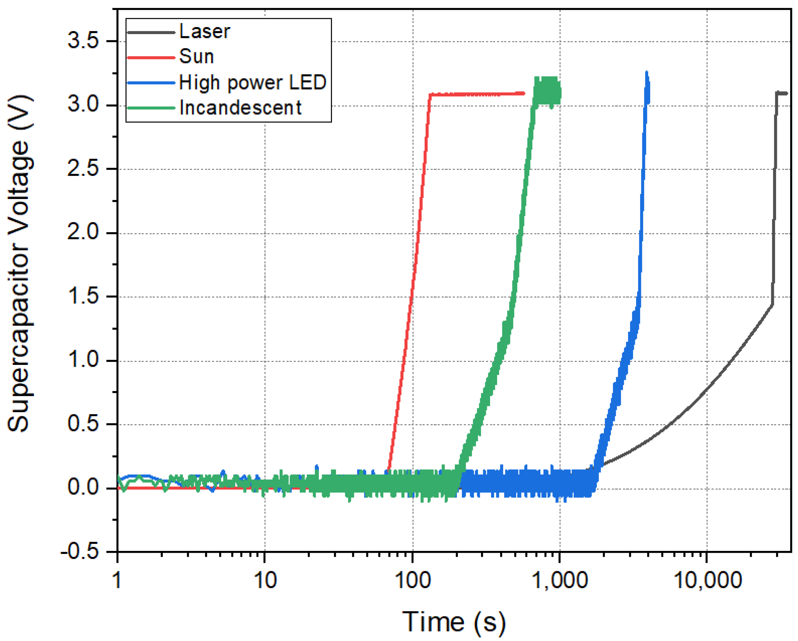
3.1. Energy Harvesting

Figure 5 shows the charging of the system’s supercapacitor using sunlight and various light sources placed 30 cm from the solar panel, including a 430-nm blue laser diode, 50-W LED, and a 100-W incandescent lamp. The measured illuminance from the sun during the experiment is 82,300 lux (obtained using an EXTECH 401025 Light Meter). The illuminance values of the LED and incandescent lamp are 11,300 and 2860 lux, respectively.
The fastest charging is when the device is directly exposed to sunlight. Charging the device using a 430-nm laser takes the longest. Besides the low lux output of the laser compared to the other light sources, the collimation nature of laser beams leads to a small filled area of the solar panel when placed at a short distance of 30 cm. The weak responsivity of silicon at the blue wavelength region also decreases the charging efficiency.

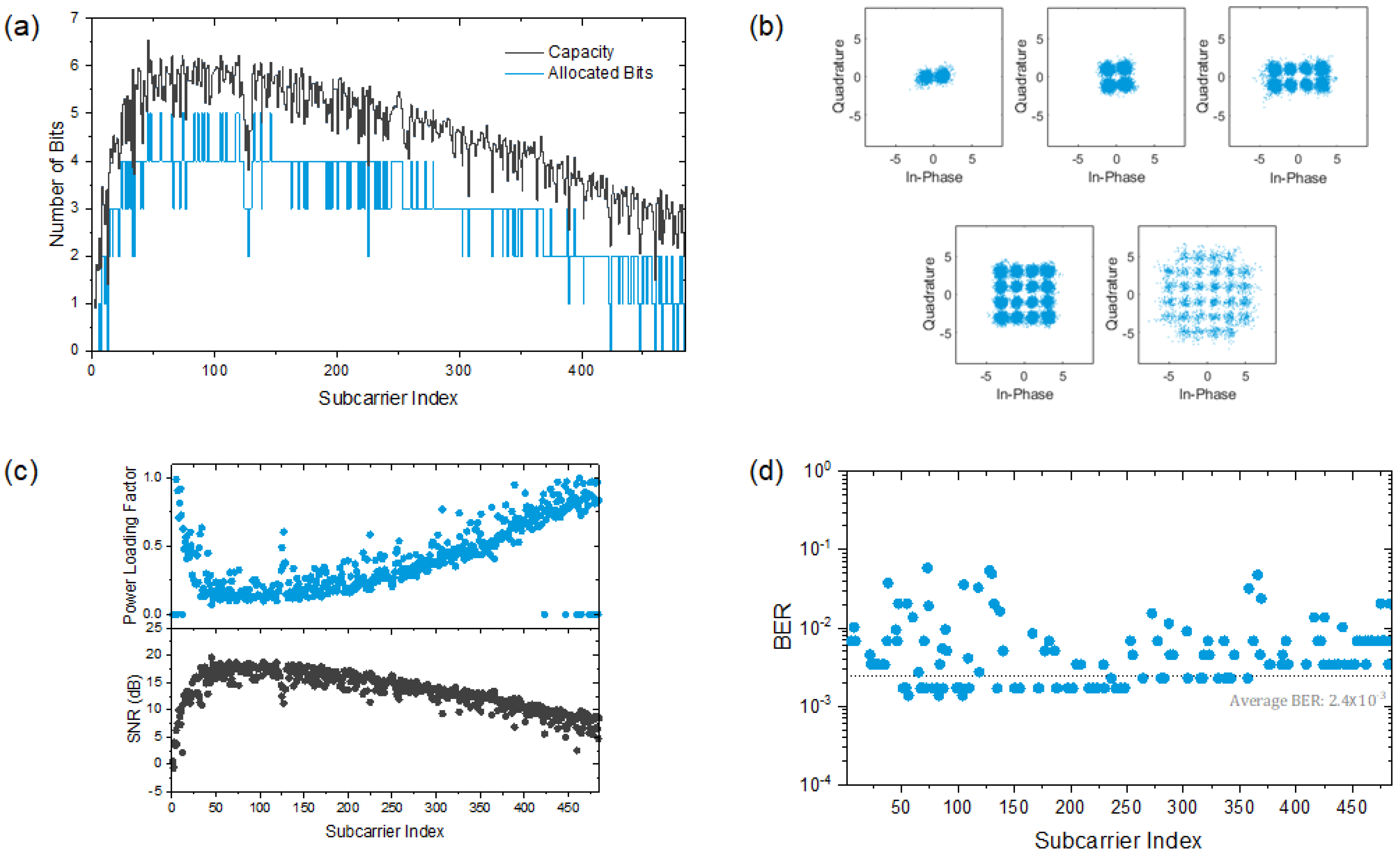
3.2. Information Decoding Capability

To test the information decoding capability of the designed system, it was placed at various distances from the transmitter in a line of sight (LoS) configuration, as depicted in Figure 6. The transmitted signals were modulated using a quadrature amplitude modulation (QAM) OFDM modulation scheme with adaptive bit and power loading. The signals were sent using an arbitrary waveform generator (AWG, Keysight 33600A) with a sampling frequency, f AWG , set to 1 Msample/s. The bias tee combines the modulation signal with the DC bias from a power supply (Agilent E3649A) to drive the 430-nm laser diode. The receiving circuit was connected to an oscilloscope (Tektronix MSO 4104) using a low power probe to collect the received signal at a sampling rate of 2.5 Msample/s and then process it offline using MATLAB®.
A test OFDM signal with a 16-QAM modulation was initially generated following the block diagram in Figure 6. A pseudo-random binary sequence (PRBS) was generated and modulated using QAM. A serial to parallel conversion was then performed. Hermitian symmetry was applied before the inverse fast Fourier Transform (IFFT) to output real values. The size of the IFFT is N F F T and was set to 1024. After that, a cyclic prefix whose length was set to 10 was added to limit intersymbol interference and simplify the equalization process on the receiver side. The parallel sequence was then converted into a serial sequence which was then sent by the AWG to the laser diode through the bias tee.
After the signal was received, it was resampled and synchronized. The serial sequence was then converted to parallel, and the cyclic prefix was removed. FFT was performed, and the symbols were extracted by removing the Hermitian symmetry symbols. Single-tap channel equalization was used after channel estimation was performed based on the training symbols. The symbols were then demodulated and converted to a serial stream of bits, which was then compared to the transmitted signal to determine the bit error rate (BER). All reported data rates were achieved with a BER below the 7%-overhead forward error correction (FEC) BER limit ( 3.8 × 10 3 ). The number of allocated bits per subcarrier was obtained from the channel capacity, as can be seen from Figure 7a, and the received QAM constellations are illustrated in Figure 7b. The power loading factor and the estimated SNR for each subcarrier are shown in Figure 7c. The BER for each sub-carrier is shown in Figure 7d.
The system performances at different distances are given in Table 2. The gross data rate, G D R , is calculated as:
G D R = f AWG N FFT + CP i = 1 N S C log 2 ( M i ) ,
where CP is the cyclic prefix length and N S C = 485 is the number of the subcarriers, M i = 2 b is the QAM order of the ith subcarrier, and b is the number of bits allocated to that subcarrier. The net data rate is calculated by accounting for the training symbols used for channel estimation and synchronization and the 7% FEC overhead. The highest data rate of 1.3 Mbps is obtained at a distance of 2 m from the transmitter. A net data rate of 0.79 Mbps is reached at 20 m.

3.3. Detecting UAV Movements

One of the main applications for a self-powered probe with SLIPT capability is monitoring the environment and activity in harsh or inaccessible locations. For that, the probe needs to be able to be woken up from external sources, such as movement. In this scenario, we demonstrate how to wake up the system with a drone. The device is always set to sleep mode, and only the low-power DAC and OA are enabled to flag any interruption. When a drone flew in a proximity of 50 cm from the sensor, as seen in Figure 8a, the system was woken up. The oscilloscope outputs of the IR sensor and the interruption are shown in Figure 8b.
This experimental test demonstrates the potential use of SLIPT for IoT powering and data collection using UAVs. A UAV can depart from a base station, locate (using global positioning system coordinates, for example), wake up an IoT device, read its information, and power it using LEDs or any other light source. The UAV can also transmit any data while powering the system, for example, sending operation commands or updating software while wireless powering the device’s battery.

4. Discussion

SLIPT is a promising technique and has great potential in the design of next-generation IoT devices. In this section, we discuss some of the key elements mainly associated with the available SC technologies that may lead to the deployment of SLIPT systems.

4.1. Active Area vs. Data Rate

Mono-crystalline and multi-crystalline Si SCs are reaching their theoretical efficiency limits. Some novel SC technologies, GaAs SCs, for example, can offer a large 3-dB-bandwidth [7] but at the expense of the detection area. However, using a large array of these SCs that can be controlled independently can provide a large detection area while offering a large detection bandwidth. A comparison between the active areas of various SC technologies and the demonstrated date rates in the literature can be seen in Table 3. Using large active area receivers can ease the strong requirements of alignment in FSO and increase the resilience to beam wandering effects arising from atmospheric turbulence [18]. Using solar panels has been equally shown to be helpful to detect laser beams propagating through underwater channels [19]. In a harsh environment, such as the underwater, fulfilling the pointing, acquisition, and tracking (PAT) is challenging given the presence of turbulence arising from random variation of the refractive index in the propagation media. Relying on large-area solar panels can help relax PAT for underwater optical wireless communication but at the expense of the data rate that is constrained by the resistance-capacitance limit. OFDM-based modulation can provide access to higher data rates compared to what is provided by OOK. Another idea to investigate is integrating fused tapered optical fibers with small-active area SCs. This technique has been proven to significantly increase the field of view of small-active area OWC receivers [20]. Due to their weak wavelength dependence, tapered fiber bundles can be potentially used for different SC technologies.

4.2. Novel SC Materials for Higher Efficiency

Progress in material science can lead to higher efficiency, including those matching the FSO wavelength windows for long-range transmissions, particularly around the 1550 nm frequency. III-V material-based SCs are showing rapid improvement due to their potential in providing high power conversion efficiency compared to other technologies and could find potential uses in SLIPT IoTs that can be connected using FSO links. Perovskite materials can provide highly-efficient SCs that can co-exist with VLC technology. Making perovskite SCs more stable is the next step for their potential use in outdoor conditions. In order to be used for IoT devices in a large-scale manner, the cost of III-V and perovskite should be comparable to SC ones. Another opportunity for higher energy harvesting while using SLIPT is through shape optimization of solar cells during the manufacturing process as demonstrated in [21], where the authors used neural networks to optimize the shape of organic solar cells to improve the conversion efficiency.

5. Conclusions

In summary, we provided an overview of the SLIPT background and the co-existence of this technology with OWC systems. We also demonstrated a self-powered system that can harvest energy for various light sources and detect signals modulated using an OFDM modulation. A net data rate of 1.3 Mbps was reported using 16-QAM OFDM scheme with an adaptive data loading (bit and power loading) algorithm at a distance of 2 m with an average BER of 2.4 × 10 3 . The designed system was equally able to detect the movements of a UAV using an IR motion sensor. Our demonstrations can be of interest to next-generation autonomous IoT devices. Finally, a discussion on the progress of SC technology and the practicality of the wide-scale deployment of SLIPT-based IoTs was included.

Author Contributions

Conceptualization, J.I.D.O.F. and A.T.; methodology, J.I.D.O.F., O.A. and A.T.; software, J.I.D.O.F. and O.A.; validation, J.I.D.O.F., O.A. and A.T.; formal analysis, J.I.D.O.F., O.A. and A.T.; investigation, J.I.D.O.F., O.A. and A.T.; resources, B.S.O., M.-S.A. and K.N.S.; data curation, J.I.D.O.F., O.A. and A.T.; writing—original draft preparation, J.I.D.O.F., O.A. and A.T.; writing—review and editing, B.S.O., M.-S.A. and K.N.S.; visualization, J.I.D.O.F., O.A., A.T., B.S.O., M.-S.A. and K.N.S.; supervision, B.S.O., M.-S.A. and K.N.S.; project administration, B.S.O., M.-S.A. and K.N.S.; funding acquisition, B.S.O., M.-S.A. and K.N.S. All authors have read and agreed to the published version of the manuscript.

Funding

This research was funded by King Abdullah University of Science and Technology.

Data Availability Statement

Data available on request from the authors.

Conflicts of Interest

The authors declare no conflict of interest.

Abbreviations

The following abbreviations are used in this manuscript:
ACAlternating Current
ADCAnalog-to-Digital Converter
AWGArbitrary Waveform Generator
DCDirect Current
EHEnergy Harvesting
FECForward Error Correction
FSOFree Space Optics
GaAsGallium Arsenide
IDInformation Decoding
IoTInternet of Things
IoUTInternet of Underwater Things
LDLaser Diode
LEDLight Emitting Diode
LoSLine of Sight
MPPTMaximum Power Point Tracking
OFDMOrthogonal Frequency Division Multiplexing
OOKOn-Off Keying
OAOperational Amplifier
OWCOptical Wireless Communication
PRBSPseudo-random Binary Sequence
PSoCProgrammable System on Chip
QAMQuadrature Amplitude Modulation
RFRadio Frequency
SCSolar Cell
SLIPTSimultaneous Lightwave and Information Transfer
SPSolar Panel
SWIPTSimultaneous Wireless Information and Power Transfer
TIATransimpedance Amplifier
UAVUnmanned Aerial Vehicle
UWOCUnderwater Wireless Optical Communication
VLCVisible Light Communication

References

  1. Ponnimbaduge Perera, T.D.; Jayakody, D.N.K.; Sharma, S.K.; Chatzinotas, S.; Li, J. Simultaneous wireless information and power transfer (SWIPT): Recent advances and future challenges. IEEE Commun. Surv. Tutor. 2018, 20, 264–302. [Google Scholar] [CrossRef] [Green Version]
  2. Lu, X.; Wang, P.; Niyato, D.; Kim, D.I.; Han, Z. Wireless charging technologies: Fundamentals, standards, and network applications. IEEE Commun. Surv. Tutor. 2016, 18, 1413–1452. [Google Scholar] [CrossRef] [Green Version]
  3. Chiaraviglio, L.; Elzanaty, A.; Alouini, M.S. Health risks associated with 5G exposure: A view from the communications engineering perspective. IEEE Open J. Commun. Soc. 2021, 2, 2131–2179. [Google Scholar] [CrossRef]
  4. Kim, S.M.; Won, J.S. Simultaneous reception of visible light communication and optical energy using a solar cell receiver. In Proceedings of the 2013 International Conference on ICT Convergence (ICTC), Jeju Island, Korea, 14–16 October 2013; pp. 896–897. [Google Scholar]
  5. Wang, Z.; Tsonev, D.; Videv, S.; Haas, H. On the design of a solar-panel receiver for optical wireless communications with simultaneous energy harvesting. IEEE J. Sel. Areas Commun. 2015, 33, 1612–1623. [Google Scholar] [CrossRef]
  6. Zhang, S.; Tsonev, D.; Videv, S.; Ghosh, S.; Turnbull, G.A.; Samuel, I.D.W.; Haas, H. Organic solar cells as high-speed data detectors for visible light communication. Optica 2015, 2, 607–610. [Google Scholar] [CrossRef] [Green Version]
  7. Fakidis, J.; Videv, S.; Helmers, H.; Haas, H. 0.5-Gb/s OFDM-based laser data and power transfer using a GaAs photovoltaic cell. IEEE Photonics Technol. Lett. 2018, 30, 841–844. [Google Scholar] [CrossRef] [Green Version]
  8. Fakidis, J.; Helmers, H.; Haas, H. Trade-Off between energy harvesting and data communication towards a 1 Gb/s laser and photovoltaic link. In Proceedings of the Optical Wireless Fiber Power Transmission Conference, Yokohama, Japan, 21–23 April 2020; pp. 1–3. [Google Scholar]
  9. Fakidis, J.; Helmers, H.; Haas, H. Simultaneous wireless data and power transfer for a 1-Gb/s GaAs VCSEL and photovoltaic link. IEEE Photonics Technol. Lett. 2020, 32, 1277–1280. [Google Scholar] [CrossRef]
  10. Mica, N.A.; Bian, R.; Manousiadis, P.; Jagadamma, L.K.; Tavakkolnia, I.; Haas, H.; Turnbull, G.A.; Samuel, I.D.W. Triple-cation perovskite solar cells for visible light communications. Photonics Res. 2020, 8, A16–A24. [Google Scholar] [CrossRef]
  11. de Oliveira Filho, J.I.; Trichili, A.; Ooi, B.S.; Alouini, M.S.; Salama, K.N. Toward self-Powered internet of underwater things devices. IEEE Commun. Mag. 2020, 58, 68–73. [Google Scholar] [CrossRef]
  12. Uysal, M.; Ghasvarianjahromi, S.; Karbalayghareh, M.; Diamantoulakis, P.D.; Karagiannidis, G.K.; Sait, S.M. SLIPT for underwater visible light communications: Performance analysis and optimization. IEEE Trans. Wirel. Commun. 2021, 20, 6715–6728. [Google Scholar] [CrossRef]
  13. Haas, H.; Videv, S.; Das, S.; Fakidis, J.; Stewart, H. Solar cell receiver free-space optical for 5G backhaul. In Proceedings of the 2019 Optical Fiber Communications Conference and Exhibition (OFC), San Diego, CA, USA, 3–7 March 2019; pp. 1–3. [Google Scholar]
  14. Das, S.; Poves, E.; Fakidis, J.; Sparks, A.; Videv, S.; Haas, H. Towards energy neutral wireless communications: Photovoltaic cells to connect remote areas. Energies 2019, 12, 3772. [Google Scholar] [CrossRef] [Green Version]
  15. Filho, J.I.D.O.; Trichili, A.; Ooi, B.S.; Alouini, M.S.; Salama, K.N. Self-powered weather station for remote areas and difficult-access locations. Opt. Express 2022, 30, 2668–2679. [Google Scholar] [CrossRef]
  16. What Is Maximum Power Point Tracking MPPT. Available online: https://www.solar-electric.com/learning-center/mppt-solar-charge-controllers.html/ (accessed on 18 April 2021).
  17. Adamo, F.; Attivissimo, F.; Di Nisio, A.; Spadavecchia, M. Characterization and testing of a tool for photovoltaic panel modeling. IEEE Trans. Instrum. Meas. 2011, 60, 1613–1622. [Google Scholar] [CrossRef]
  18. Trichili, A.; Cox, M.A.; Ooi, B.S.; Alouini, M.S. Roadmap to free space optics. J. Opt. Soc. Am. B 2020, 37, A184–A201. [Google Scholar] [CrossRef]
  19. Kong, M.; Sun, B.; Sarwar, R.; Shen, J.; Chen, Y.; Qu, F.; Han, J.; Chen, J.; Qin, H.; Xu, J. Underwater wireless optical communication using a lens-free solar panel receiver. Opt. Commun. 2018, 426, 94–98. [Google Scholar] [CrossRef]
  20. Alkhazragi, O.; Trichili, A.; Ashry, I.; Ng, T.K.; Alouini, M.S.; Ooi, B.S. Wide-field-of-view optical detectors using fused fiber-optic tapers. Opt. Lett. 2021, 46, 1916–1919. [Google Scholar] [CrossRef] [PubMed]
  21. Sciuto, G.L.; Capizzi, G.; Coco, S.; Shikler, R. Geometric shape optimization of organic solar cells for efficiency enhancement by neural networks. In Advances on Mechanics, Design Engineering and Manufacturing; Springer: Berlin/Heidelberg, Germany, 2017; pp. 789–796. [Google Scholar]
Figure 1. Illustration of a generic network architecture of self-powered devices.
Energies 15 02814 g001
Figure 2. Solar panel circuit model for (a) energy harvesting and (b) information decoding.
Energies 15 02814 g002
Figure 3. Time switching solar panel circuit model.
Energies 15 02814 g003
Figure 4. Illustration of the system design. IR: infrared; PSOC: programmable system on chip; DAC: digital-to-analog converter; TIA: transimpedance amplifier; OA: operational amplifier.
Energies 15 02814 g004
Figure 5. A 470 mF supercapacitor charging using sunlight and various light sources placed 30 cm from the solar panel.
Energies 15 02814 g005
Figure 6. Data transfer experimental setup with the OFDM block diagram. The distance between the 430-nm laser source was set to 2, 10, and 20 m.
Energies 15 02814 g006
Figure 7. Communication characteristics using an OFDM modulation scheme. (a) Channel capacity and the bit loading scheme for all used subcarriers. (b) Received m-QAM constellations. (c) The power loading factor and the SNR for each subcarrier. (d) The BER for each subcarrier.
Energies 15 02814 g007
Figure 8. (a) Diagram of the wake-up using a UAV, (b) the device being woken up by a drone, (c) oscilloscope outputs of the infrared sensor (in light blue) and the interruption (in dark blue).
Energies 15 02814 g008
Table 1. Comparison between different SLIPT configurations.
ApproachTime SwitchingPower SplittingSpace Splitting
Hardware ComplexityLowHighModerate
Real-Time EH and IDNoYesYes
MPPTYesNoYes
CostLowModerateHigh
Table 2. Performance at different propagation distances.
Distance (m)Gross Data Rate (Mbps)Net Data Rate (Mbps)
21.41.3
101.050.95
200.870.79
Table 3. Comparison between data rates in SLIPT-based demonstrations in the literature.
Reference SC Technology Active Area (mm 2 ) Max Data Rate (Mbps)
[5] Multi-crystalline Si 43,200 a 11.84 (OFDM)
[6] Organic (PTB7:PC 71 BM) 8 34.2 (OFDM)
[9] GaAs 0.8 1000 (OFDM)
[10] Triple-cation perovskite 6.5 56 (OFDM)
This work Mono-crystalline Si 3850 1.4 (OFDM)
a Size of the full solar panel. Considered active area in the experimental demonstration is significantly smaller.
Publisher’s Note: MDPI stays neutral with regard to jurisdictional claims in published maps and institutional affiliations.

