
Influence of As-N Interstitial Complexes on Strain Generated in GaAsN Epilayers Grown by AP-MOVPE

 , , and
Abstract
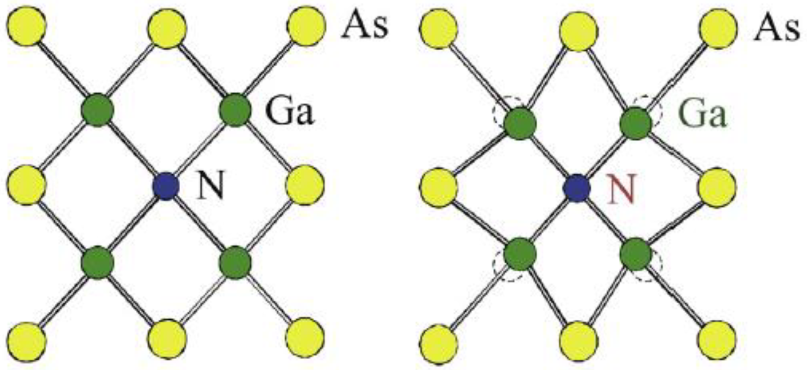
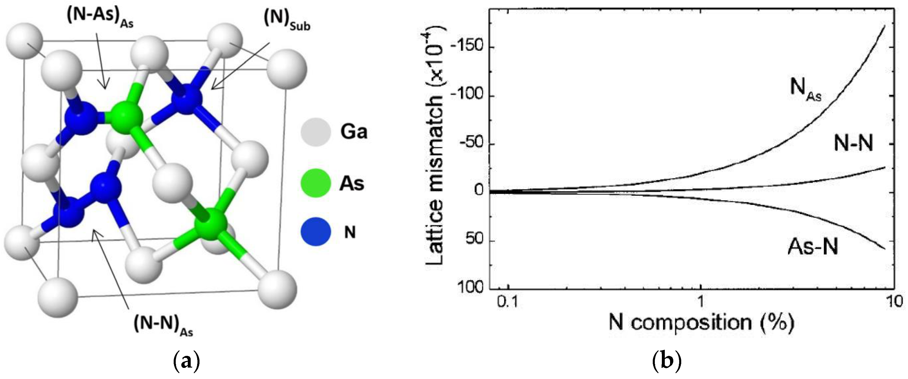
:1. Introduction
2. Experimental Details
3. Results and Discussion
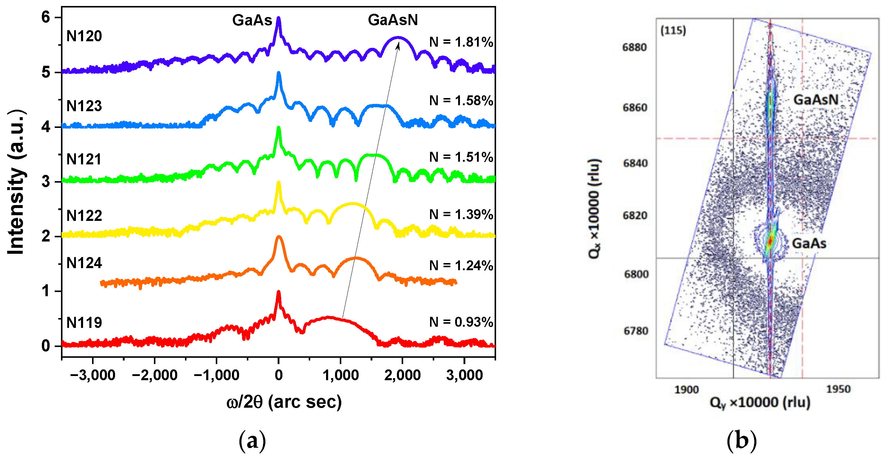
3.1. High Resolution X-ray Diffraction Measurements
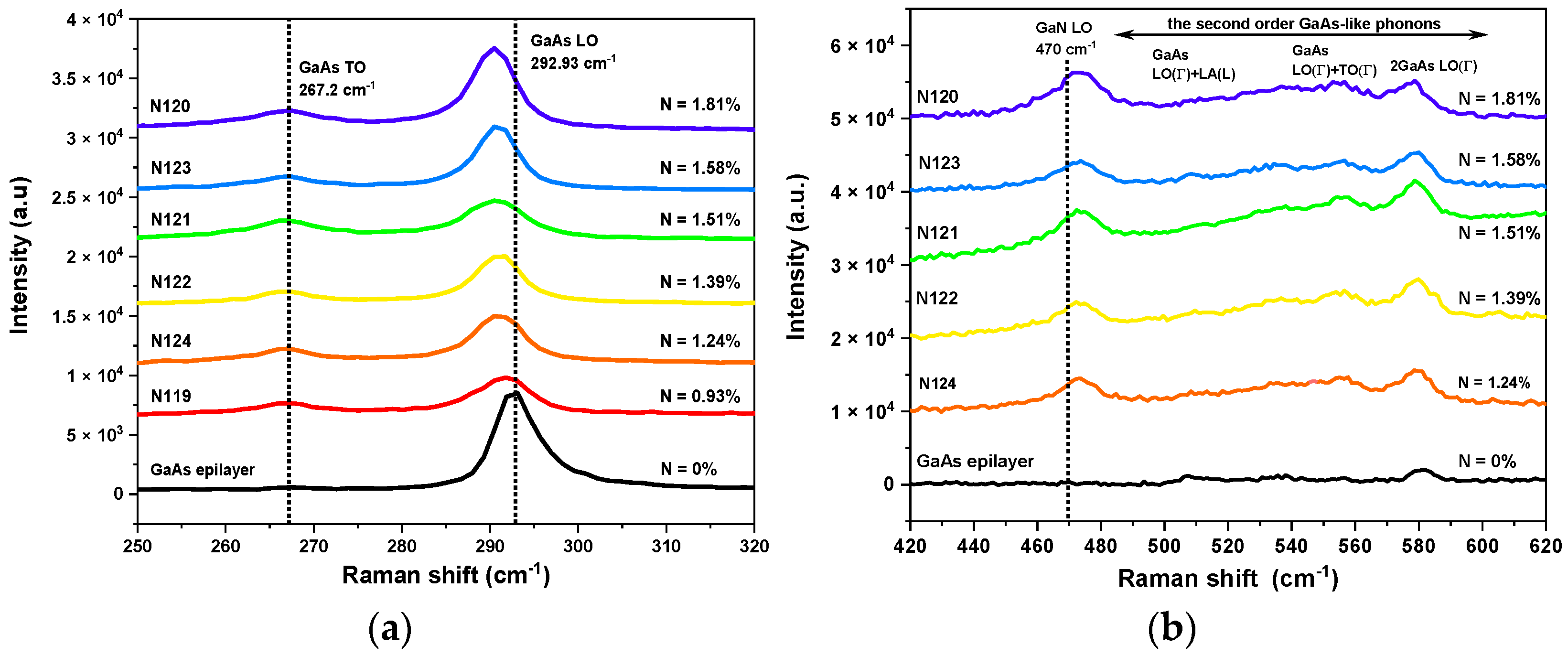
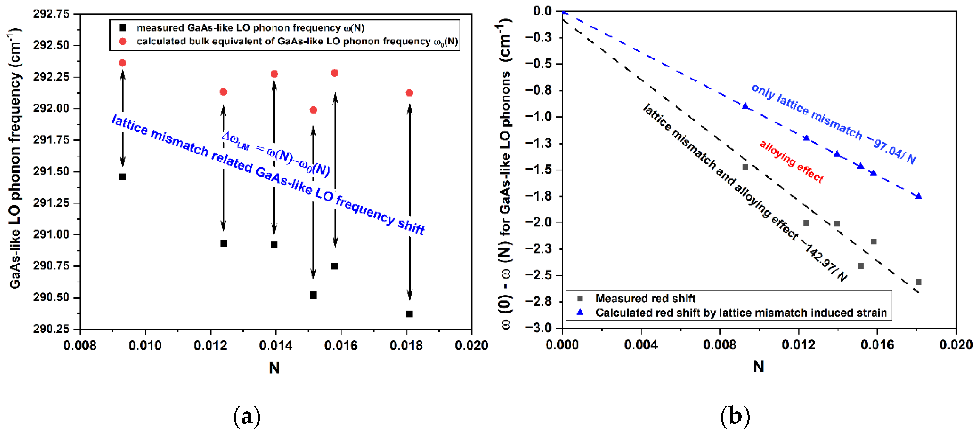
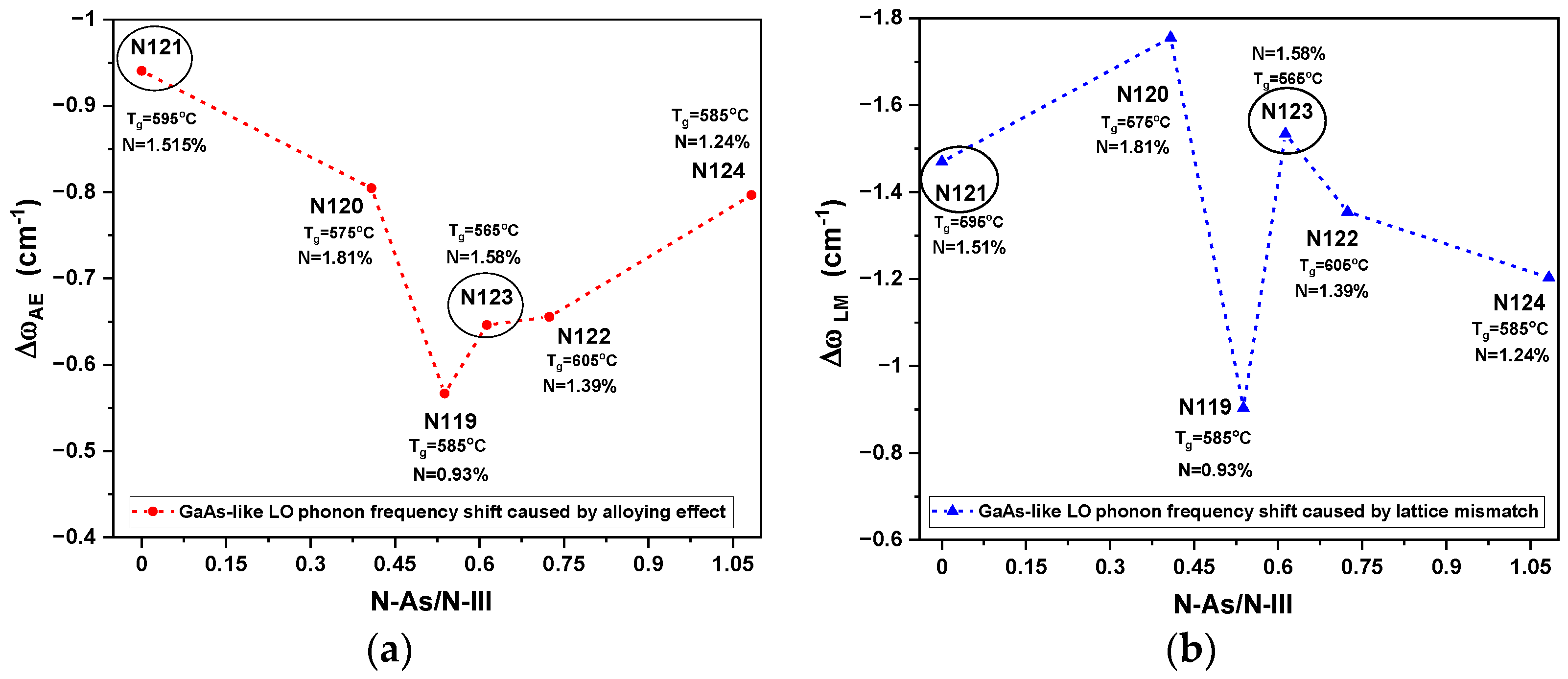
3.2. Raman Measurements and Average Strain Determination
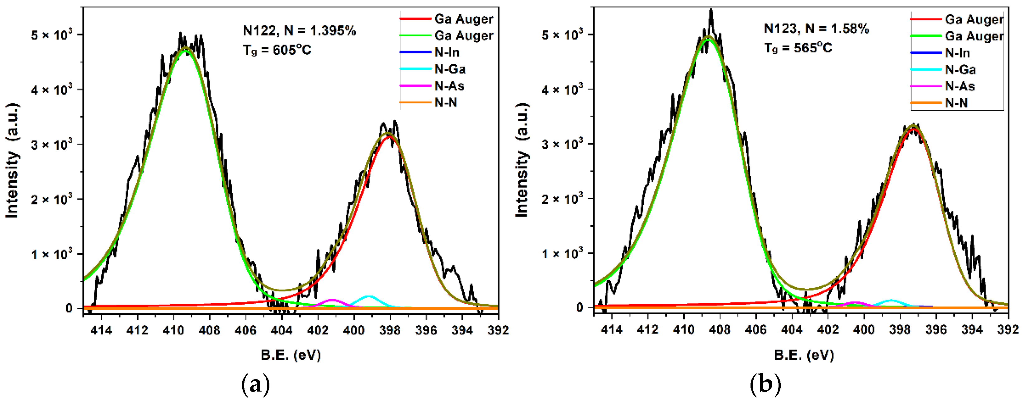
3.3. XPS Spectra Analysis
4. Conclusions
Author Contributions
Funding
Institutional Review Board Statement
Informed Consent Statement
Data Availability Statement
Acknowledgments
Conflicts of Interest
References
- Beyer, A.; Stolz, W.; Volz, K. Metastable cubic zinc-blende III/V semiconductors: Growth and structural characteristics. Prog. Cryst. Growth Charact. Mater. 2015, 61, 46–62. [Google Scholar] [CrossRef]
- Stringfellow, G. Epitaxial growth of metastable semiconductor alloys. J. Cryst. Growth 2021, 564, 126065. [Google Scholar] [CrossRef]
- Walukiewicz, W.; Zide, J.M.O. Highly Mismatched Semiconductor Alloys: From Atoms to Devices. J. Appl. Phys. 2020, 127, 010401. [Google Scholar] [CrossRef] [Green Version]
- Ściana, B.; Radziewicz, D.; Dawidowski, W.; Bielak, K.; Szyszka, A.; Kopaczek, J. Impact of gallium concentration in the gas phase on composition of InGaAsN alloys grown by AP-MOVPE correlated with their structural and optical properties. J. Mater. Sci. Mater. Electron. 2019, 30, 16216–16225. [Google Scholar] [CrossRef] [Green Version]
- Shan, W.; Yu, K.M.; Walukiewicz, W.; Wu, J.; Ager, J.; Haller, E.E. Band anticrossing in dilute nitrides. J. Phys. Condens. Matter 2004, 16, S3355–S3372. [Google Scholar] [CrossRef] [Green Version]
- Bank, S.R.; Bae, H.; Goddard, L.L.; Yuen, H.B.; Wistey, M.A.; Kudrawiec, R.; Harris, J.S. Recent Progress on 1.55-μm Dilute-Nitride Lasers. IEEE J. Quantum Electron. 2007, 43, 773–785. [Google Scholar] [CrossRef]
- Tansu, N.; Yeh, J.-Y.; Mawst, L. High-performance 1200-nm InGaAs and 1300-nm InGaAsN quantum-well lasers by metalorganic chemical vapor deposition. IEEE J. Sel. Top. Quantum Electron. 2003, 9, 1220–1227. [Google Scholar] [CrossRef]
- Tomic, F.S.; O’Reilly, E.P.; Fehse, R.; Sweeney, S.; Adams, A.; Andreev, A.; Choulis, S.; Hosea, T.J.C.; Riechert, H. Theoretical and experimental analysis of 1.3-μm InGaAsN/GaAs lasers. IEEE J. Sel. Top. Quantum Electron. 2003, 9, 1228–1238. [Google Scholar] [CrossRef]
- Polojärvi, V.; Aho, A.; Tukiainen, A.; Raappana, M.; Aho, T.; Schramm, A.; Guina, M. Influence of As/group-III flux ratio on defects formation and photovoltaic performance of GaInNAs solar cells. Sol. Energy Mater. Sol. Cells 2016, 149, 213–220. [Google Scholar] [CrossRef]
- Dawidowski, W.; Ściana, B.; Zborowska-Lindert, I.; Mikolášek, M.; Kováč, J.; Tłaczała, M. Tunnel junction limited performance of InGaAsN/GaAs tandem solar cell. Sol. Energy 2020, 214, 632–641. [Google Scholar] [CrossRef]
- Gonzalo, A.; Stanojević, L.; Marrón, D.F.; Guzman, A.; Hierro, A.; Ulloa, J. 1 eV GaAsSbN-based solar cells for efficient multi-junction design: Enhanced solar cell performance upon annealing. Sol. Energy 2021, 221, 307–313. [Google Scholar] [CrossRef]
- Kunert, B.; Volz, K.; Stolz, W. Properties and Laser Applications of the GaP-Based (GaNAsP)-Material System for Integration to Si Substrates. In Dilute III-V Nitride Semiconductors and Material Systems. Materials Science; Erol, A., Ed.; Springer: Berlin/Heidelberg, Germany, 2008; Volume 105. [Google Scholar] [CrossRef]
- Liebich, S.; Zimprich, M.; Beyer, A.; Lange, C.; Franzbach, D.J.; Chatterjee, S.; Hossain, N.; Sweeney, S.; Volz, K.; Kunert, B.; et al. Laser operation of Ga(NAsP) lattice-matched to (001) silicon substrate. Appl. Phys. Lett. 2011, 99, 071109. [Google Scholar] [CrossRef] [Green Version]
- Hume-Rothery, W.; Smallman, R.W.; Haworth, W.C. The Structure of Metals and Alloys; Institute of Metals and the Institution of Metallurgists: London, UK, 1969. [Google Scholar]
- Li, J.; Han, X.; Dong, C.; Fan, C. Formation energies of substitutional NAs and split interstitial complexes in dilute GaAsN alloys with different growth orientations. Appl. Phys. A 2018, 124, 108. [Google Scholar] [CrossRef]
- Zhang, S.B.; Wei, S.-H. Nitrogen Solubility and Induced Defect Complexes in Epitaxial GaAs:N. Phys. Rev. Lett. 2001, 86, 1789–1792. [Google Scholar] [CrossRef] [PubMed]
- Li, W.; Pessa, M.; Likonen, J. Lattice parameter in GaNAs epilayers on GaAs: Deviation from Vegard’s law. Appl. Phys. Lett. 2001, 78, 2864–2866. [Google Scholar] [CrossRef]
- Jen, T.; Vardar, G.; Wang, Y.Q.; Goldman, R.S. Identifying the dominant interstitial complex in dilute GaAsN alloys. Appl. Phys. Lett. 2015, 107, 221904. [Google Scholar] [CrossRef]
- Querales-Flores, J.D.; Ventura, C.I.; Fuhr, J.D. Effect of N interstitial complexes on the electronic properties of GaAs1−xNx alloys from first principles. Phys. Rev. Mater. 2019, 3, 024602. [Google Scholar] [CrossRef] [Green Version]
- Kosa, A.; Stuchlikova, L.; Harmatha, L.; Mikolasek, M.; Kovac, J.; Ściana, B.; Dawidowski, W.; Radziewicz, D.; Tlaczala, M. Defect distribution in InGaAsN/GaAs multilayer solar cells. Sol. Energy 2016, 132, 587–590. [Google Scholar] [CrossRef]
- Tan, L.J.J.; Soong, W.M.; David, J.P.R.; Ng, J.S. Dark Current Mechanism in Bulk GaInNAs Lattice Matched to GaAs. IEEE Trans. Electron Devices 2010, 58, 103–106. [Google Scholar] [CrossRef]
- Loke, W.K.; Yoon, S.F.; Wicaksono, S.; Tan, K.H.; Lew, K.L. Defect-induced trap-assisted tunneling current in GaInNAs grown on GaAs substrate. J. Appl. Phys. 2007, 102, 054501. [Google Scholar] [CrossRef]
- Dawidowski, W.; Ściana, B.; Bielak, K.; Mikolášek, M.; Drobný, J.; Serafińczuk, J.; Lombardero, I.; Radziewicz, D.; Kijaszek, W.; Kósa, A.; et al. Analysis of Current Transport Mechanism in AP-MOVPE Grown GaAsN p-i-n Solar Cell. Energies 2021, 14, 4651. [Google Scholar] [CrossRef]
- Unitfit for Windows, The Art of Peak Fit. Available online: https://www.unifit-software.de/publications.html (accessed on 1 March 2022).
- Giulotto, E.; Geddo, M. Micro-Raman Mapping of the Strain Field in GaAsN/GaAsN:H Planar Heterostructures: A Brief Review and Recent Evolution. Appl. Sci. 2019, 9, 4864. [Google Scholar] [CrossRef] [Green Version]
- Shin, H.K.; Lockwood, D.J.; Lacelle, C.; Poole, P.J. Phonons in strained In1−xGaxAs/InP epilayers. J. Appl. Phys. 2000, 88, 6423–6428. [Google Scholar] [CrossRef]
- Bellani, V.; Bocchi, C.; Ciabattoni, T.; Franchi, S.; Frigeri, P.; Galinetto, P.; Geddo, M.; Germini, F.; Guizzetti, G.; Nasi, L.; et al. Residual strain measurements in InGaAs metamorphic buffer layers on GaAs. Eur. Phys. J. B 2007, 56, 217–222. [Google Scholar] [CrossRef]
- Burns, G.; Wie, C.R.; Dacol, F.H.; Pettit, G.D.; Woodall, J.M. Phonon shifts and strains in strain-layered (Ga1−xInx)As. Appl. Phys. Lett. 1987, 51, 1919–1921. [Google Scholar] [CrossRef] [Green Version]
- Jainy, S.C.; Willander, M.; Maes, H. Stresses and strains in epilayers, stripes and quantum structures of III–V compound semiconductors. Semicond. Sci. Technol. 1996, 11, 641–671. [Google Scholar] [CrossRef]
- Anastassakis, E. Stress measurements using Raman scattering. In Proceedings of the 19th European Solid State Device Research Conference, Berlin, Germany, 11–14 September 1989; Volume 90-11, pp. 298–326. [Google Scholar]
- Giulotto, E.; Geddo, M.; Patrini, M.; Guizzetti, G.; Sharma, M.S.; Capizzi, M.; Polimeni, A.; Pettinari, G.; Rubini, S.; Felici, M. Strain related relaxation of the GaAs-like Raman mode selection rules in hydrogenated GaAs1−xNx layers. J. Appl. Phys. 2019, 125, 175701. [Google Scholar] [CrossRef]
- Prokofyeva, T.; Sauncy, T.; Seon, M.; Holtz, M.; Qiu, Y.; Nikishin, S.; Temkin, H. Raman studies of nitrogen incorporation in GaAs1−xNx. Appl. Phys. Lett. 1998, 73, 1409–1411. [Google Scholar] [CrossRef]
- Chang, W.; Lin, J.; Zhou, W.; Chua, S.J.; Feng, Z.C. Photoluminescence and photoelectron spectroscopic analysis of InGaAsN grown by metalorganic chemical vapor deposition. Appl. Phys. Lett. 2001, 79, 4497–4499. [Google Scholar] [CrossRef]
- Veal, T.D.; Mahboob, I.; Piper, L.F.J.; Ashley, T.; Hopkinson, M.; McConville, C.F. Electron spectroscopy of dilute nitrides. J. Phys. Condens. Matter 2004, 16, S3201–S3214. [Google Scholar] [CrossRef]
- Lay, T.S.; Kuo, W.T.; Chen, L.P.; Lai, Y.H.; Hung, W.H.; Wang, J.S.; Chi, J.Y.; Shih, D.K.; Lin, H.H. Probing the electronic structures of III-V-nitride semiconductors by x-ray photoelectron spectroscopy. J. Vac. Sci. Technol. B 2004, 22, 1491–1494. [Google Scholar] [CrossRef]
- López-Escalante, M.; Ściana, B.; Dawidowski, W.; Bielak, K.; Gabás, M. Atomic configurations in AP-MOVPE grown lattice-mismatched InGaAsN films unravelled by X-ray photoelectron spectroscopy combined with bulk and surface characterization techniques. Appl. Surf. Sci. 2018, 433, 1–9. [Google Scholar] [CrossRef] [Green Version]
- Milanova, M.; Donchev, V.; Kostov, K.L.; Alvarez, D.A.; Terziyska, P.; Avdeev, G.; Valcheva, E.; Kirilov, K.; Georgiev, S. Study of GaAsSb:N bulk layers grown by liquid phase epitaxy for solar cells applications. Mater. Res. Express 2019, 6, 075521. [Google Scholar] [CrossRef]
- Milanova, M.; Donchev, V.; Kostov, K.L.; Alonso-Álvarez, D.; Valcheva, E.; Kirilov, K.; Asenova, I.; Ivanov, I.G.; Georgiev, S.; Ekins-Daukes, N. Experimental study of the effect of local atomic ordering on the energy band gap of melt grown InGaAsN alloys. Semicond. Sci. Technol. 2017, 32, 085005. [Google Scholar] [CrossRef]
- Chen, X.; Zhang, D.; Jin, Y.; Li, J.; Teng, J.; Yakovlev, N. Effect of rapid thermal annealing on behavior of nitrogen in GaAsN alloys. J. Cryst. Growth 2013, 362, 197–201. [Google Scholar] [CrossRef]
- Hecht, J.-D.; Frost, F.; Hirsch, D.; Neumann, H.; Schindler, A.; Preobrajenski, A.B.; Chassé, T. Interstitial nitrogen induced by low-energy ion beam nitridation of AIII–BV semiconductor surfaces. J. Appl. Phys. 2001, 90, 6066–6069. [Google Scholar] [CrossRef]
- Jin, Y.; Tang, X.; Teng, J.; Zhang, D. Optical properties and bonding behaviors of InSbN alloys grown by metal-organic chemical vapor deposition. J. Cryst. Growth 2015, 416, 12–16. [Google Scholar] [CrossRef]


| Element | Covalent Radius (pm) | Lattice Constant Ga-Compound (nm) | Electronegativity |
|---|---|---|---|
| N | 75 | 0.452 | 3.04 |
| P | 106 | 0.54505 | 2.19 |
| As | 119 | 0.565325 | 2.18 |
| Sb | 138 | 0.609593 | 2.05 |
| Bi | 146 | 0.637 (theory) | 2.02 |
| Sample | Tg (°C) | τ (min) | N (%) | d (nm) |
|---|---|---|---|---|
| N123 | 565 | 20 | 1.58 | 100 |
| N120 | 575 | 20 | 1.81 | 130 |
| N119 | 585 | 10 | 0.93 | 65 |
| N124 | 585 | 20 | 1.24 | 102 |
| N121 | 595 | 20 | 1.51 | 126 |
| N122 | 605 | 20 | 1.39 | 97 |
| Sample | N (%) | N-As/N-III | ω (0) (cm−1) | ω (N) (cm−1) | ω0 (N) (cm−1) | Δω AE ω0 (N)-ω (0) (cm−1) | Δω LM ω (N)-ω0 (N) (cm−1) |
|---|---|---|---|---|---|---|---|
| N121 | 1.51 | 0 | 292.93 | 290.52 | 291.99 | −0.94 | −1.47 |
| N120 | 1.81 | 0.408 | 290.37 | 292.13 | −0.81 | −1.75 | |
| N119 | 0.93 | 0.538 | 291.46 | 292.36 | −0.57 | −0.90 | |
| N123 | 1.58 | 0.613 | 290.75 | 292.28 | −0.65 | −1.53 | |
| N122 | 1.39 | 0.724 | 290.92 | 292.27 | −0.66 | −1.35 | |
| N124 | 1.24 | 1.083 | 290.93 | 292.13 | −0.80 | −1.20 |
Publisher’s Note: MDPI stays neutral with regard to jurisdictional claims in published maps and institutional affiliations. |
© 2022 by the authors. Licensee MDPI, Basel, Switzerland. This article is an open access article distributed under the terms and conditions of the Creative Commons Attribution (CC BY) license (https://creativecommons.org/licenses/by/4.0/).
Share and Cite
Ściana, B.; Dawidowski, W.; Radziewicz, D.; Jadczak, J.; López-Escalante, M.C.; González de la Cruz, V.; Gabás, M. Influence of As-N Interstitial Complexes on Strain Generated in GaAsN Epilayers Grown by AP-MOVPE. Energies 2022, 15, 3036. https://doi.org/10.3390/en15093036
Ściana B, Dawidowski W, Radziewicz D, Jadczak J, López-Escalante MC, González de la Cruz V, Gabás M. Influence of As-N Interstitial Complexes on Strain Generated in GaAsN Epilayers Grown by AP-MOVPE. Energies. 2022; 15(9):3036. https://doi.org/10.3390/en15093036
Chicago/Turabian StyleŚciana, Beata, Wojciech Dawidowski, Damian Radziewicz, Joanna Jadczak, Mari Cruz López-Escalante, Victor González de la Cruz, and Mercedes Gabás. 2022. "Influence of As-N Interstitial Complexes on Strain Generated in GaAsN Epilayers Grown by AP-MOVPE" Energies 15, no. 9: 3036. https://doi.org/10.3390/en15093036