Article

Multiple-Source Single-Output Buck-Boost DC–DC Converter with Increased Reliability for Photovoltaic (PV) Applications

by
Mohamed S. Elrefaey
1,
Mohamed E. Ibrahim
1,2,
Elsayed Tag Eldin
3,*,
Hossam Youssef Hegazy
4,
Elwy E. El-Kholy
2 and
Samia Abdalfatah
4
1
Faculty of Technological Industry and Energy, Delta Technological University (DTU), Quwaysna 32631, Egypt
2
Faculty of Engineering, Menoufia University, Shebin El-Kom 32511, Egypt
3
Faculty of Engineering and Technology, Future University in Egypt, Cairo 11835, Egypt
4
Faculty of Industrial Education, Helwan University, Cairo 11835, Egypt
*
Author to whom correspondence should be addressed.
Energies 2023, 16(1), 216; https://doi.org/10.3390/en16010216
Submission received: 9 December 2022 / Revised: 19 December 2022 / Accepted: 21 December 2022 / Published: 25 December 2022
(This article belongs to the Section F3: Power Electronics)

Abstract

:
This paper presents an improved topology for a DC–DC converter suitable for PV applications. The proposed converter has the ability to be energized from multiple DC sources. Hence, it can be energized from two, three or a higher number of sources according to the number of modules adopted in its design. The proposed converter can supply a single load with DC power at a voltage lower or higher than the summation of all excitation DC voltages with a non-reversed voltage polarity at its output. Moreover, it provides a more reliable operation compared to other DC–DC converters due to its ability for operation with partial failures in its exciting sources. In this paper, the theoretical discussion of the proposed converter is presented considering its construction and its principle of operation. The performance of the proposed converter is theoretically evaluated using simulation based on power simulation (PSIM) software at different conditions. The performance of the converter is theoretically evaluated using PSIM considering photovoltaic (PV) sources as input sources for the proposed converter to show its validity for renewable energy applications. For more evaluation, experimental work is carried out by building a prototype and testing it at different operating conditions.

1. Introduction

Power electronic converters are extensively used in a lot of applications. These converters can be classified to DC–DC, AC–DC, AC–AC and DC–AC converters. DC–DC is considered one of the most common converters in the field that can be used in different applications. These applications include use as battery chargers [1,2,3], DC motor drives [4,5,6], electric vehicles [7,8,9,10,11], renewable energy applications [12,13,14,15,16,17], light-emitting diode (LED) lamp drivers [18,19,20] and other applications. In fact, a buck-boost converter is a DC–DC converter that finds a continuous development due to its advantages, such as its ability to give output voltages lower or higher than its input one. Therefore, continuous development of these converters has received great interest from researchers and scientists in this field.
Considering the developments in DC–DC buck-boost converters, a proposed topology is suggested in [21] as a modified version of the traditional buck-boost converter. This topology has the advantage of an improved voltage gain; however, it suffers from high voltage stresses on its switches, and its output has a reversed voltage polarity if compared to its input as well. In [22], another topology has the merits of high voltage gain, and a continuous input current is presented. However, it also suffers from the use of several storage devices as well as its output voltage having a reversed polarity compared to its input. In [23], another buck-boost converter is introduced. This converter has the advantage of low voltage stresses on its switches and the use of a reduced number of storage devices. However, this converter has some disadvantages such as the limited voltage gain, high ripples and the increased switching protection issues. In [24,25,26], buck-boost DC–DC converters with quadratic voltage gains are developed. They are found to have good performance during their step-up conversion. However, they have limited step-down capability. In [27,28], semi quadratic buck-boost DC–DC converters are developed. They have good performance during their operation in bucking and stepping modes. However, their input currents are discontinuous, and they do not have a common ground. In [29], two DC–DC converters are suggested with very high voltage gains, but there is a great difficulty in their control methods. A switched capacitor is another topology used to achieve a buck-boost DC–DC converter [30,31,32,33]. Although, it gives good performance and its control method finds great development, it depends on a high number of power electronic switches that increases its cost.
Looking to the continuous developments in buck-boost DC–DC converter topologies, there is a need for a DC–DC converter topology that has the ability to operate in a reliable manner with the occurrence in partial failures in the exciting sources. Hence, this feature will be very useful in different applications, especially the applications that depend on renewable energy sources. Therefore, this paper presents an improved topology for a DC–DC converter suitable for PV applications. The proposed converter has the ability to be energized from multiple DC sources. Hence, it can be energized from two, three or a higher number of sources according to the number of modules adopted in its design. The proposed converter can supply a single load with DC power at a voltage lower or higher than the summation of all excitation DC voltages with a non-reversed voltage polarity at its output. Moreover, it provides a more reliable operation compared to other DC–DC converters due to its ability for operation with partial failures in its exciting sources. In this paper, the theoretical discussion of the proposed converter is presented considering its construction and its principle of operation. The performance of the proposed converter is theoretically evaluated using a simulation based on power simulation (PSIM) software at different conditions. The performance of the converter is theoretically evaluated using PSIM considering photovoltaic (PV) sources as input sources for the proposed converter to show its validity for renewable energy applications. For more evaluation, experimental work is carried out by building a prototype and testing it at different operating conditions.
This paper is organized as follows:
  • Section 1: the present section that introduces a review for pre-published research in the field of this study.
  • Section 2: this section presents the circuit diagram as well as the principle of operation of the proposed buck-boost DC–DC converter.
  • Section 3: this section presents the suggested applications for the proposed DC–DC converter.
  • Section 4: the simulation study using PSIM software is carried out considering different cases.
  • Section 5: the experimental validation of the suggested converter is introduced.
  • Section 6: the conclusions from the study are summarized.

2. The Proposed Buck-Boost DC–DC Converter

Figure 1 shows the circuit diagram of the suggested buck-boost DC–DC converter. The suggested DC–DC converter is excited from more than one source. The present discussion is focused only on a converter supplied from only two sources, for reasons of clarity. The construction of this converter can be briefly explained as follows:
  • The number of power electronic switches (IGBTs, MOSFETs, …… etc.) used in the proposed converter equals the number of the exciting sources. So, two switches are used in Figure 1 as two sources are considered.
  • The number of storage elements (inductors and capacitors) equals the number of input sources. Moreover, in Figure 1, two inductors and two capacitors are used, as the number of input sources is equal to two.
  • A diode is used in each stage to allow the charging of the stage capacitor from the stored energy in the stage inductor without reversal of charging direction (diodes D1 and D2 in Figure 1).
  • A diode is used between the capacitors of each consecutive stage to allow the discharge of the capacitors in series in only one direction through the load connected at the converter output (diode D3 in Figure 1).
  • Moreover, a diode is connected between each two consecutive sources to provide isolation between each of the two consecutive stages to prevent the disturbances in current paths during switching process (diode D4 in Figure 1).
The proposed converter switches are controlled using only a single pulse. This means that all converter switches are turned-on or turned-off at the same instants. This feature is considered an advantage as there is no need for drive circuits’ complexity for the suggested converter. The improved step-up and step-down capabilities are achieved due to the series connection of the converter capacitors, as will be declared in the next discussions. Moreover, the reliability of this converter is considered high, such as during the occurrence of partial failure or a failure in one of the exciting sources; the converter can operate with a satisfactory performance, as will be illustrated in the next sections. To understand the operation of the proposed converter, consider Figure 2. This figure shows the modes of operation of the adopted converter. Hence, Figure 2a shows the paths of current flow in the converter during the on state of the two stages that occur simultaneously. The current path is denoted by a blue color for the first stage; however, it is denoted by a red color for the second stage. During this condition (on state for the two switches), currents rise in the two inductors due to the formed opposite polarity, as shown in Figure 2a. These polarities are reversed when the switches are switched off according to Lenz’s law, and each stage capacitor is charged with the shown polarity declared in Figure 2b. Moreover, the current paths through this mode are characterized using the same colors (blue and red for the two stages). The two capacitors are discharged in series through the load as indicated in Figure 2c.
Considering continuous current through the two inductors, Figure 3 shows the waveforms of the current passing through the inductor of the first stage and the voltage across it with the variation of the driving pulse from on to off states. The current rises through the inductor during this condition, and its rate of change can be computed from:
d i l d t = V 1 L
where il is the current passing through the inductor, V1 is the input voltage to the first stage and L is the inductance of the first-stage inductor.
At the end of the on period (from 0 to DT), the increase in inductor current can be computed as:
0 D T d i l = 0 D T V 1 L d t = V 1 D T L
where D is the duty ratio of the driving pulse, and T is the period of it.
When the switch of this stage is turned off, the current through the inductor decreases with a rate that can be computed from:
d i l d t = V c 1 L
where Vc1 is the output voltage at the capacitor of the first stage.
At the end of the on period (from DT to T), the decrease in inductor current can be computed as:
0 1 D T d i l = 0 1 D T V c 1 L d t = V c 1 1 D T L
Considering a lossless converter, V 1 D T L V c 1 1 D T L = 0 .
Therefore, the voltage gain of the first stage can be computed as:
V c 1 V 1 = D 1 D
Similarly, the voltage gain of the second stage can be computed from:
V c 2 V 2 = D 1 D
where Vc2 is the output voltage at the capacitor of the second stage, and V2 is the exciting voltage of it.
Considering the two stages are similar at which VC1=VC2 and V1=V2, the voltage gain for the two stages can be computed as:
V o l t a g e   G a i n = 2 D 1 D
Generally, if the number of stages becomes n, the voltage gain is computed from:
V o l t a g e   G a i n = n D 1 D
Figure 4 shows the variation of the proposed converter gain with the variation of the duty ratio (D) considering different numbers of stages. The gain is considered as the ratio of the converter output voltage to the input voltage of only one-stage to show the effect of the number of stages on the gain. From this figure, it can be seen that the converter can give voltages lower or higher than the input voltage. Moreover, the increase in the number stages (n) increases the output voltage value.
Considering discontinuous currents pass through the two inductors, Figure 5 shows the waveforms of the current passing through the inductor of the first stage and the voltage across it with the variation of the driving pulse from on to off states. The maximum inductor current (Imax) can be computed from:
I m a x = V 1 D T L
During the off state, the inductor current falls to zero after a time of δT. Therefore:
I m a x V c 1 δ T L = 0
From the above two equations, δ can be computed from:
δ = V 1 D V c 1
The average load current (Io) can be computed as:
I o = I m a x 2 δ
So,
  I o = V 1 2 D 2 T 2 L V c 1
Therefore, the output voltage gain of the first stage can be computed as:
V c 1 V 1 = V 1 D 2 T 2 L I o
The voltage gain of the second stage can be computed using the same formula derived in (14). So, considering n stages, the voltage gain can be calculated using:
V o l t a g e   G a i n = n V 1 D 2 T 2 L I o
From the above equation, voltage gain from the converter and of course the output voltage depend on some other factors such as the inductance value of the inductor not only on the duty ratio compared to the continuous inductor current mode.
Regarding the switching and the dynamic losses of the converter, the following power losses can be considered:
  • The conduction losses of the power electronic switches due to their resistances.
  • The switching losses of power electronic switches due to high frequencies.
  • The diode losses due to its forward resistance and its voltage drop.
  • The inductor losses due to its resistance.
  • The power losses due to the resistance of filtering capacitor.
The conduction losses in each switch (Ps) come due to its resistance (rs), and it can be computed for each switch from:
P S = r s I s 2 = D r s I o 2 1 D 2
where Io is the load current in A.
The switching losses due to switching frequency (fs) can be computed from [34]:
P s w = f s C V 1 + V c 1 2 = f s C R L P O D 2
The losses in each diode (Pd) due to its voltage drop (Vd) and its conduction resistance (rf) can be computed from [34]:
P d = r f I o 2 1 D + V d I o
The inductor losses (PL) due to its resistance (rl) can be computed from:
P L = r l I o 2 1 D 2
Moreover, the losses in each capacitor due to its resistance (rc) are computed as:
P c = D r c I o 2 1 D
The total losses in the suggested converter are equal to the summation of all aforementioned losses multiplied by n to consider the losses in all stages.

3. Suggested Application of the Proposed Converter

The proposed multiple-source DC–DC buck-boost converter can be used in a lot of applications. In our opinion, this converter will be valuable if it is used in one of the recent modern applications. This application is a battery charging system for electric vehicles from PV systems. Hence, it is suggested to use PV panels as input sources for the proposed converter. The DC output of the converter is used to charge the electric vehicle’s batteries as shown schematically in Figure 6. The use of this system has several advantages. The capability of this converter to buck or boost the input voltage is an advantage, since the output voltage of the converter can be efficiently regulated with the variation of sun illumination. However, the major advantage of this converter is its increased reliability. When partial failure occurs in the exciting PV panels or in converter switches or other components, the converter can still charge the electric vehicle batteries due to the presence of more than one stage. The rate of battery charge will slow down with the occurrence of partial failure, but the charging process still occurs. This means that a lower probability of system shutdown is achieved. Therefore, an increased reliability of the proposed system is obtained, which means a better service can be provided.

4. Simulation Study of the Proposed Multiple-Source Converter

The adopted DC–DC converter is simulated using power simulation (PSIM) software. Several cases are studied through the simulation. These cases are:
  • Studying the performance of the studied DC–DC converter as a two-stage converter when feeding a resistive–inductive load when excited from two DC sources.
  • Studying the performance of the suggested converter when excited from three DC sources during the excitation of a resistive–inductive load.
  • Studying the performance of the two-stage converter when feeding a resistive–inductive load considering a closed-loop voltage control system.
  • Studying the performance of the adopted converter during battery charging.
  • Studying the performance of the converter considering the two exciting sources as PV sources adopting maximum power point tracking (MPPT) control to extract maximum possible power from the PV systems.
  • Studying the ability of the suggested converter to be supplied from only one source with the same performance of multiple sources.
Considering the aforementioned cases, the two-stage converter is modeled with the parameters shown in Table 1; however, all diodes and switches are considered ideal. The obtained simulation results are presented as follows.

4.1. Performance of the Converter When Excited from Two DC Sources and Feeding a Resistive–Inductive Load

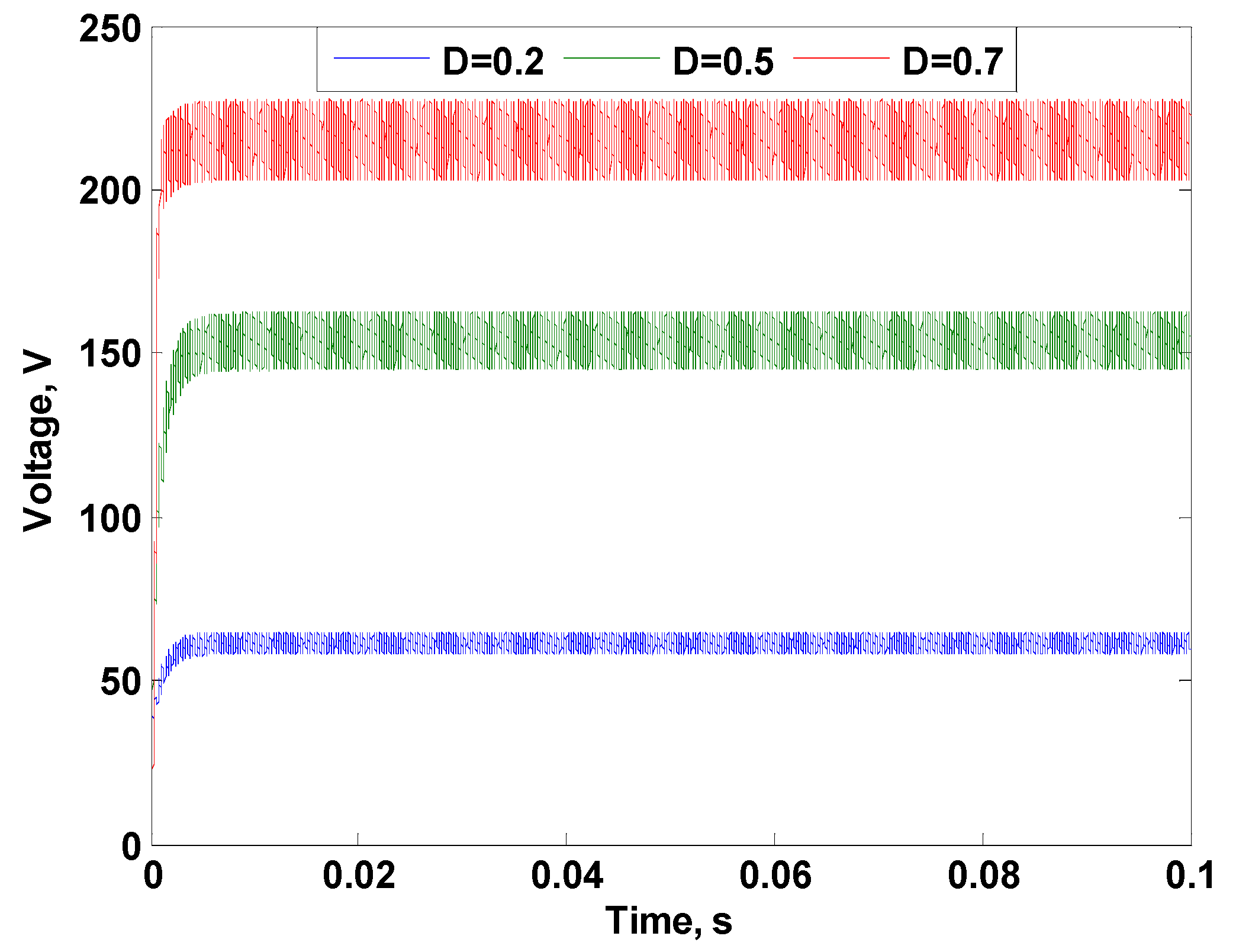
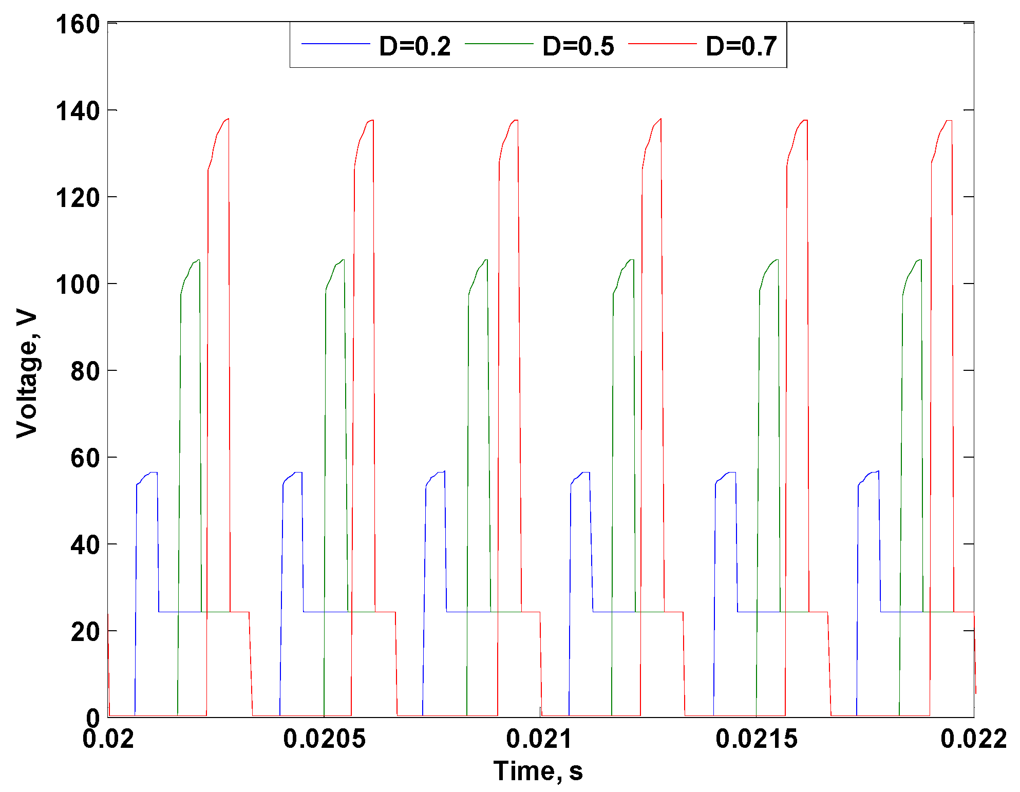
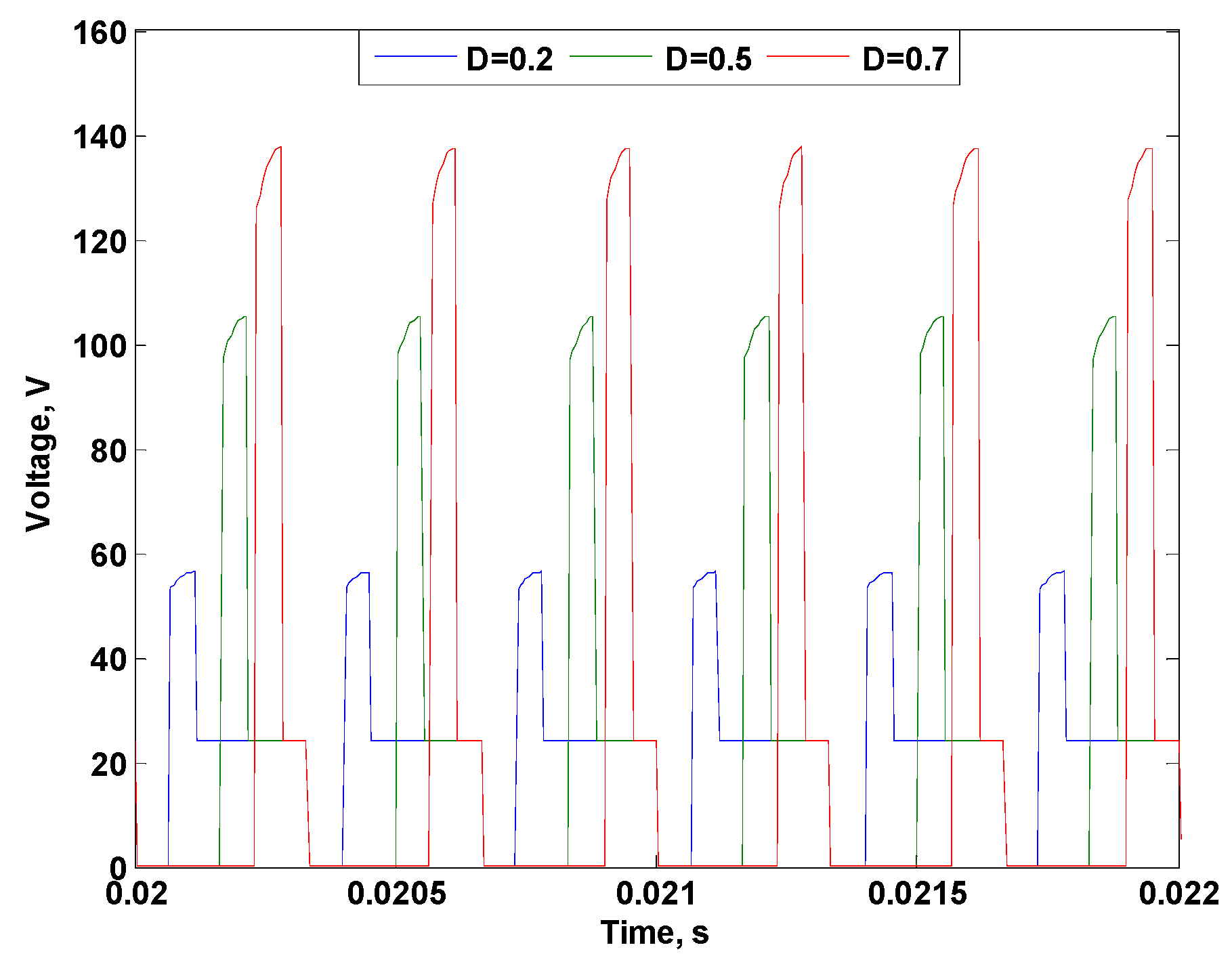
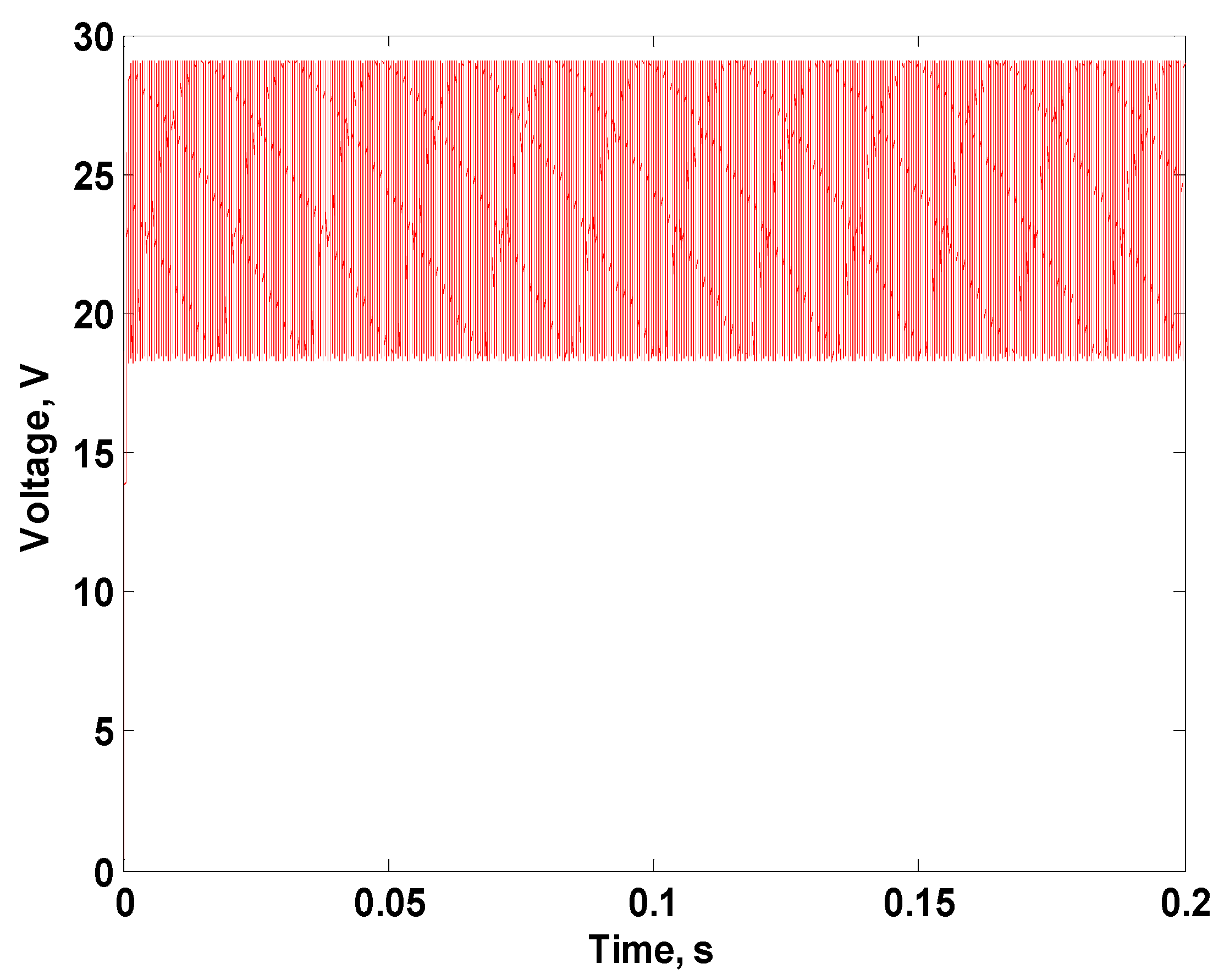
The converter is modeled using PSIM software with the parameters shown previously in Table 1. In this section, the supplying sources are considered two ideal DC sources; each has a voltage of 24 V. However, the load is taken as a resistive–inductive load with a load resistance of 50 Ω and an inductance of 5 mH. Figure 7 shows the output voltages at the DC–DC converter output considering duty ratios of 0.2, 0.5 and 0.7 at a switching frequency of 3 kHz. From this figure, the increase in the duty ratio results in increased output voltage. Hence, at duty ratios of 0.2, 0.5 and 0.7, the output voltages are equal to 62 V, 154.6 V and 216 V, respectively. Considering the same conditions, Figure 8 and Figure 9 show the voltages at the terminals of the first-stage and second-stage capacitors, respectively, at the same duty ratios. From these figures, the voltages across the two capacitors having approximately the same values at the same operating conditions. Moreover, the summation of these voltages is equal to the output voltage at the converter terminals shown in Figure 7 at each corresponding duty ratio. This result validates the concept used with this converter at which the stage capacitors are discharged in series through the load. Voltage stresses on the converter switches are of important factors that determine the converter’s good design. So, Figure 10 and Figure 11 show the voltage stresses on the two switches used with the converter. From these figures, it can be seen that the maximum voltage stress on the two-stage switches is similar at all duty ratios. Moreover, the maximum voltage stress on each switch is less than the output voltage from the converter at all adopted duty ratios. Hence, the maximum voltage stress on each switch is slightly higher than one-half of the output voltage at the converter terminals at each duty ratio. This means that low voltage stresses are achieved for the used switches in the adopted converter.

4.2. Performance of the Suggested Converter When Excited from Three DC Sources during the Excitation of a Resistive–Inductive Load

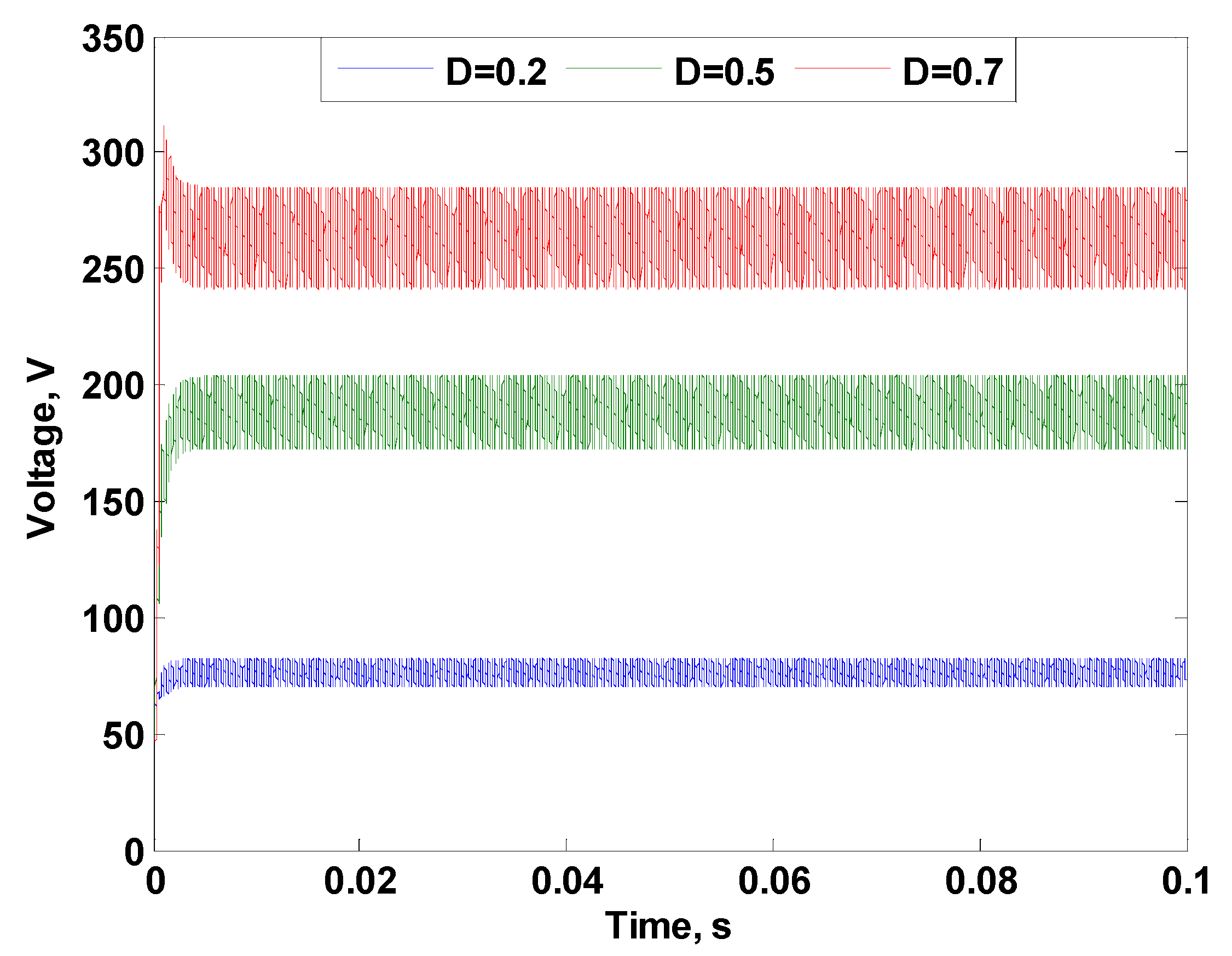
In this section, the ability of the suggested converter to be excited from more than two sources is presented. Figure 12 shows the circuit diagram of the adopted converter considering its excitation from three DC sources. The converter is simulated using PSIM software using the same parameters listed in Table 1. The used three sources for excitation each have 24 V DC, and the simulated load is a resistive–inductive load with the same load parameters identified in Section 4.1. Figure 13 shows the output voltage from the converter considering the same duty ratios taken in Section 4.1. It is noticed that the converter gives output voltages higher than the two-stage converter as described before. Moreover, it is found that the summation of the three-stage capacitor voltages equals the output voltage at each duty ratio. However, capacitor voltages are not presented here, as the same conclusions are presented before in the above section.

4.3. Performance of the Two-Stage Converter when Excited from Two DC Sources and Feeding a Resistive–Inductive Load Considering a Closed-Loop Voltage Control

In this section, the two-stage converter with the same parameters illustrated in Section 4.1 is used. A closed-loop voltage control is evaluated in this section. The control system adopted depends on using a simple PI controller. Figure 14 shows the adopted control technique. The parameters of the used PI controller are 0.008 for its gain and 0.001 for its time constant. Moreover, the control system uses a triangular waveform having a 3 kHz frequency to generate the driving pulse. The control system uses a reference DC voltage to set its value at the desired output voltage level. This reference voltage is compared to the measured output voltage at the load terminals. The error between reference and measured voltages is processed using a PI controller. The output signal from the controller is compared to a triangular waveform to generate the driving signal of the power electronic switches. Saturation is used in the control loop to limit the output voltage level at a desired threshold. Generally, the closed-loop control system is evaluated when the converter feeds the same resistive–inductive load used in the aforementioned subsection at two cases. The first case is the healthy case at which the converter is excited from two healthy 24 V DC sources. However, in the second case, a failure in the second-stage source occurs that causes its voltage to drop to 12 V instead of 24 V. Considering the healthy condition, Figure 15 shows the output, first-stage capacitor and second-stage capacitor voltages considering a reference DC voltage is set at 100 V. From this figure, it can be shown that the output voltage successfully follows the reference voltage. However, ripples are found in the output voltage. These ripples can be reduced using higher capacitances in the converter design. Moreover, it can be seen that the voltages of the first-stage and second-stage capacitors are approximately identical, and their summation is equal to the output voltage. Figure 16 shows the first-stage and second-stage inductor currents. Approximately identical currents for the two inductors are noticed. This means that at healthy condition the two stages operate identically without overloading or stressing on one stage. Figure 17 and Figure 18 show the same results as Figure 15 and Figure 16, respectively, but considering a reference DC voltage of 200 V. The same conclusions from these figures are also obtained.
Figure 19 shows the output, first-stage capacitor and second-stage capacitor voltages considering a failure in the first-stage source when the reference voltage is set at 200 V. This failure is simulated by considering the voltage of the first-stage voltage being reduced to 12 V instead of 24 V. This can occur during the occurrence of partial failure in batteries. From this figure, the converter has the ability to follow the reference voltage. Hence, the healthy stage compensates the reduction that occurs in the faulty stage to achieve the desired reference voltage. Figure 20 shows the currents of the two inductors. At this condition, these currents are not identical, such as the healthy condition. This comes as the healthy stage compensates the faulty stage.

4.4. Studying the Performance of the Adopted Two-Stage Converter during Battery Charging

In this section, studying the performance of the adopted two-stage DC–DC converter during battery charging is presented. The battery is simulated using a DC source of 120 V to simulate ten 12 V batteries connected in series. The batteries’ total resistance is taken as 0.1 Ω. Moreover, an inductor of 5 mH is connected in series with the batteries at the converter output to achieve more smooth current at the converter output. During this study, a closed-loop current control is adopted. The same control technique used in Figure 14 is adopted. However, the reference DC voltage is replaced by a reference DC current that is compared to the measured output current instead of measured output voltage. Considering a reference current of 2 A, Figure 21 and Figure 22 show the converter voltages and the charging current, respectively. Hence, Figure 21 shows the output, first-stage capacitor and second-stage capacitor voltages. It can be seen that the voltages of the two capacitors are identical. Moreover, the voltage at the battery terminals is 120.2 V. The increase in the output voltage by 0.2 V is to charge the battery at the desired current that is shown in Figure 19. The same results are repeated again considering a charging current of 5 A. The converter voltages are shown in Figure 23; however, the charging current is shown in Figure 24. For more efficacy validation, consider a sudden failure occurs in the first-stage supply that causes its voltage to be reduced from 24 V to 12 V when the reference current is set at 5 A. At this condition, Figure 25 shows the converter voltages; however, Figure 26 shows the charging current. It is noticed that the output voltage is approximately constant at 120.5 V due to voltage compensation from the second stage. Regarding all the obtained results in this section, the adopted converter can be effectively used to charge batteries.

4.5. Studying the Performance of the Converter Considering the Two Exciting Sources as PV Sources Adopting Maximum Power Point Tracking (MPPT) Control to Extract Maximum Possible Power from the PV Systems

In this section, the two sources are replaced by two photovoltaic (PV) solar modules. The two modules have similar characteristics. The characteristics of each module are shown in Table 2. The same adopted resistive–inductive load used in the above sections is used. Moreover, maximum power point tracking (MPPT) control is adopted. The adopted MPPT method is the well-known perturb and observe technique [35]. This technique is used due to its simplicity, and there is no need to know the characteristics of the PV source. Considering these conditions, Figure 27 shows the output, first-stage capacitor and second-stage capacitor voltages. The two-capacitor voltages are identical. So, only one curve appears in the figure. Moreover, the summation of the two-capacitor voltages is equal the total output voltage as described before. Figure 28 and Figure 29 show the voltages at the terminals of the two PV sources. From these figures, the voltage of each PV source oscillates around the maximum power point voltage (24 V). This means that the maximum power point is achieved during the adopted control technique with the suggested DC–DC converter. So, it can be used with PV applications effectively, especially with its advantage to give the desired outputs with the occurrence of faults in one of the sources.

4.6. Studying the Ability of the Suggested Converter to Be Supplied from Only One Source with the Same Performance of Multiple Sources

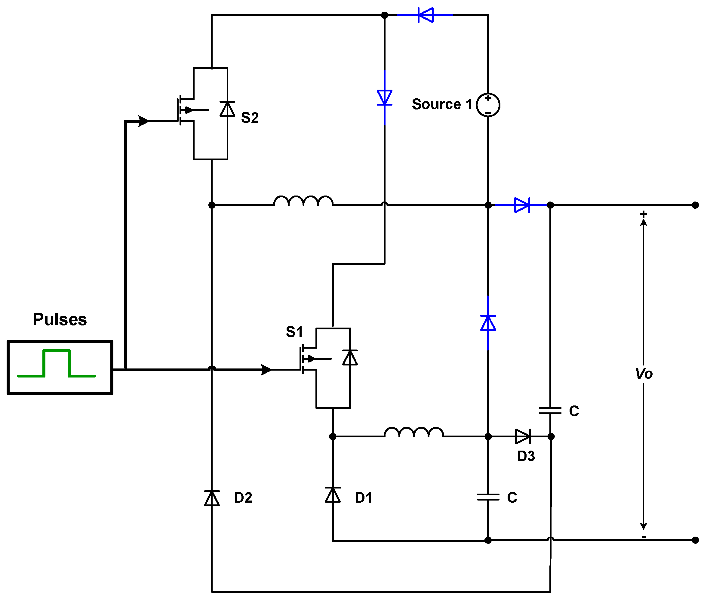
One of the important main advantages of the suggested converter is its ability to be supplied from only one source with the same performance of the multiple sources with a slight modification in its design. The modification is carried out as shown schematically in Figure 30. The modifications are carried out using four diodes, as shown by the blue color in the figure. These diodes are added to isolate between the two converter stages. So, the modification can be simply carried out, and this option can be used at the cases if only a single source is available. The modified circuit diagram is simulated using PSIM software using the same parameters and the same resistive–inductive load used in the aforementioned sections at an excitation voltage of 24 V. It is evaluated at different conditions, and the same performance is achieved if compared to the multiple-source converter. Therefore, in this section, the performance of the modified converter circuit is presented only at an open-loop condition at duty ratios of 0.2, 0.5 and 0.7 as taken before with the multiple-source circuit. However, there is no need to present the other aforementioned studied cases as the same performance is achieved. Figure 31 shows the output voltages at the terminals of the load considering the duty ratios of 0.2, 0.5 and 0.7. Figure 32 and Figure 33 show the voltages across the terminals of the first-stage capacitor as well as the second-stage capacitor at the same duty ratios, respectively. Looking to this figure, the same performance is achieved if compared to the multiple-source circuit considering the same operating conditions as depicted from Figure 7, Figure 8 and Figure 9.

5. Experimental Results

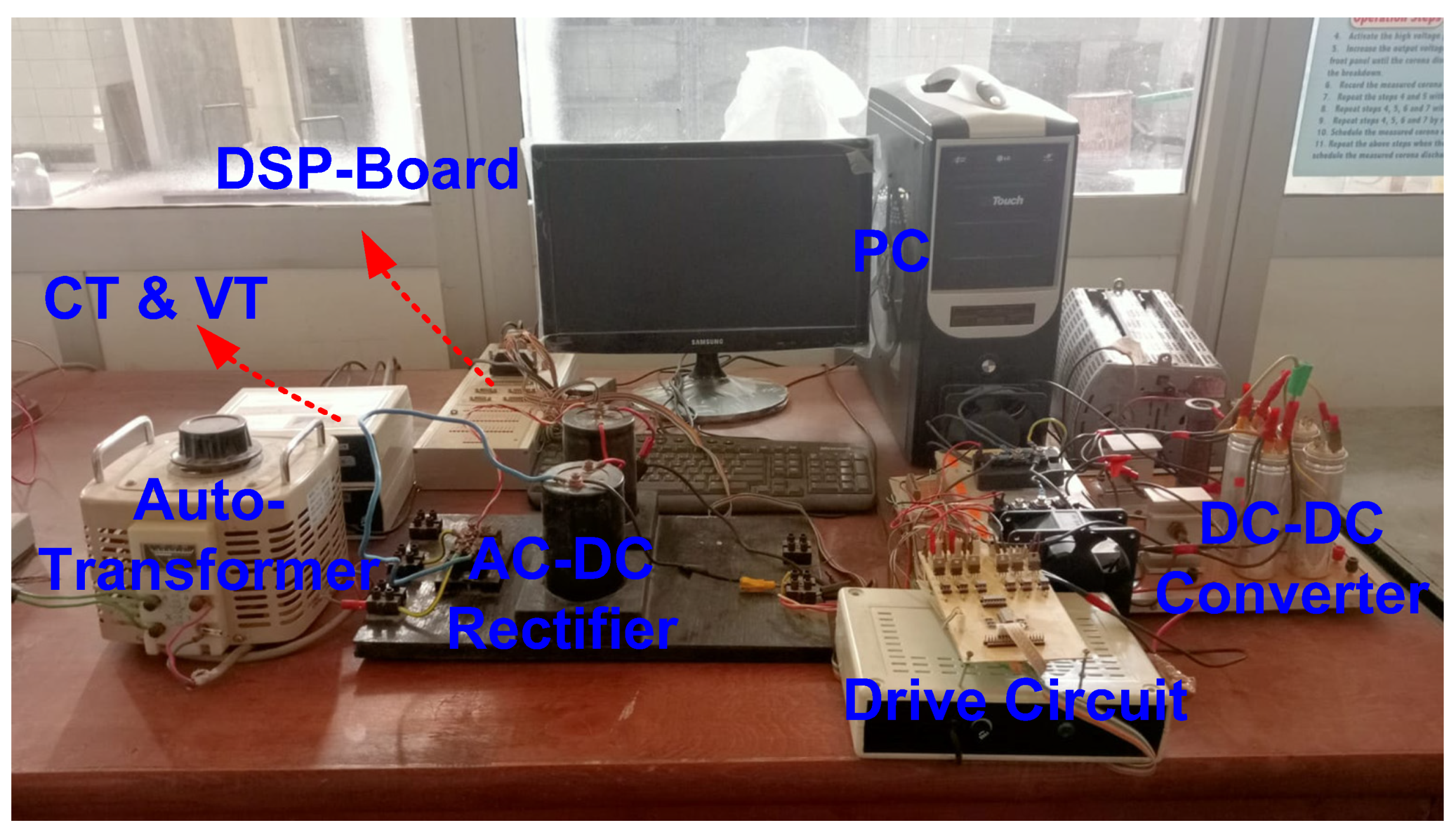
In this section, the experimental study is carried out on the modified circuit of the suggested DC–DC converter shown before in Figure 30. The modified circuit is chosen in the experimental study, as the study of the multiple-source circuit is focused on in the simulation study. Again, both circuits give the same performance as stated before. So, a prototype of the modified DC–DC buck-boost converter circuit is built as shown in the photograph of Figure 34 considering the 24 V DC source. The DC source used in the experimental study is a full-wave rectifier supplied from a single-phase auto transformer. A 500 μF capacitor is used at the DC terminals of the bridge rectifier to obtain smooth DC voltage. Considering the circuit construction, the used transistors are IGBTs, Model CM300DY-24 A Mitsubishi Electric. The two inductors have 0.1 mH inductance for each one. However, two capacitors are used; each capacitor has 450 μF capacitance and a rated voltage of 400 V. The driving pulses at the studied cases are digitally generated using a DSP-board dSpace 1104. In fact, the experimental study is carried out considering two cases. These cases are:
  • Open-loop control considering different duty ratios, 0.2, 0.5 and 0.7, with a resistive–inductive load having 100 Ω of resistance.
  • Closed-loop voltage control considering the same resistive load (100 Ω).
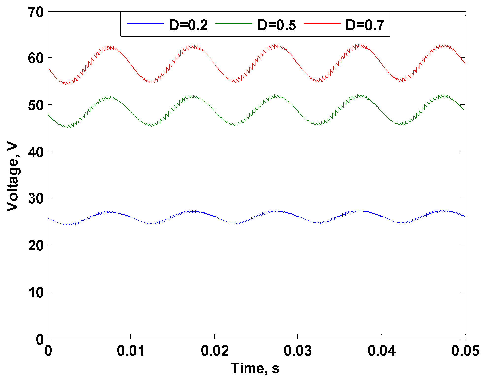
The driving pulses’ frequency is taken as 3 kHz for both studied cases. Figure 35 shows the output voltages at the load terminals at the adopted duty ratios. From the figure, the converter can give variable voltages as described before. Figure 36 and Figure 37 show the first-stage capacitor and the second-stage capacitor voltages at the same duty ratios, respectively. It can be noticed that there is small deviation between the two capacitor voltages. This deviation may come due to a presence of a small deviation in the two inductors used in the converter circuit. However, the summation of the two-capacitor voltages is equal to the output voltage at all studied duty ratios. Figure 38 shows the efficiency variation with the variation of output power considering a duty ratio of 0.5. The curve is obtained by connecting a variable resistive load at the converter terminals to achieve variable output power. From the curve, it can be seen that maximum efficiency of the converter is approximately 93%. The converter efficiency can be increased considering ferrite cores for the two inductors instead of conventional iron cores to reduce their core losses.
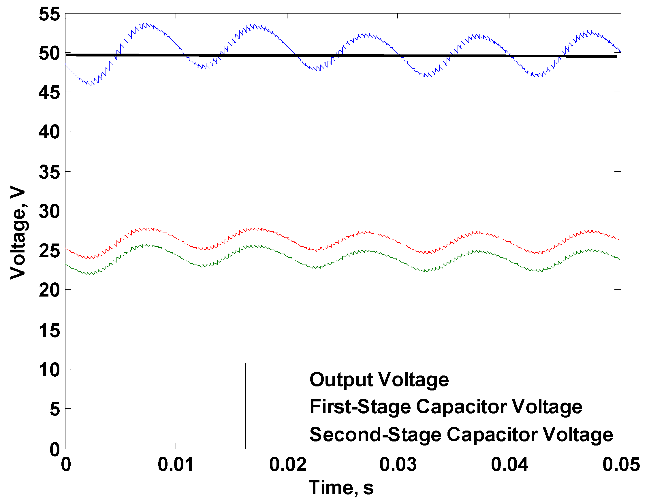
Considering the closed-loop control, a voltage transducer is used to measure the voltage at the load terminals. The reference voltage is set at 50 V. Figure 39 shows the output, first-stage capacitor and second-stage capacitor voltages for this case. It can be seen that the output voltage follows the reference signal with the presence of some ripples, which come due to the switching process. These ripples can be minimized with the increase in switching frequency. Moreover, the summation of the two capacitor voltages equals the output voltage with a presence of a small deviation between the two-capacitor voltages, which may come due to deviations in the two-stage parameters of the circuit components. Generally, the obtained experimental results validate the obtained theoretical study and prove the efficacy of the suggested DC–DC buck-boost converter.

6. Conclusions

In this paper, a proposed multiple-source DC–DC buck-boost converter has been presented. The suggested DC–DC converter has increased reliability due to its dependence on more than one stage and more than one source. The performance of this converter has been theoretically studied using PSIM software. The study has been carried out to take different operating conditions into consideration ranging from healthy to faulty conditions. Different loads have been adopted in the study such as resistive–inductive and battery loads. Different sources have been used as exciting supplies such as DC sources and PV panels. Moreover, closed-loop voltage control and closed-loop current control have been implemented, and a good performance has been achieved considering healthy and faulty conditions. It has been proven that the suggested converter can be supplied from only one source with a slight modification. This point has been evaluated theoretically, and the same performance has been achieved compared to the multiple-source converter. Finally, the efficacy of the suggested converter has been proven and validated experimentally through a prototype that has been built and tested.

Author Contributions

Conceptualization, M.S.E., M.E.I., E.T.E., H.Y.H., S.A. and E.E.E.-K.; investigation, M.S.E.; methodology, M.S.E., M.E.I., E.T.E., H.Y.H., S.A. and E.E.E.-K.; software, M.S.E.; supervision, M.E.I., E.T.E., H.Y.H. and E.E.E.-K.; validation, M.E.I., H.Y.H., S.A. and E.E.E.-K.; writing—original draft, M.S.E.; writing—review and editing, M.S.E., M.E.I., E.T.E., H.Y.H., S.A. and E.E.E.-K. All authors have read and agreed to the published version of the manuscript.

Funding

This research received no external funding.

Conflicts of Interest

The authors declare that they have no known competing financial interests or personal relationships that could have appeared to influence the work reported in this paper.

References

  1. Karneddi, H.; Ronanki, D. Bridgeless Boost-Buck based Universal PFC Converter with Wide Output Voltage for Onboard Battery Charging Applications. In Proceedings of the 2022 IEEE Energy Conversion Congress and Exposition (ECCE), Detroit, MI, USA, 9–13 October 2022; pp. 1–6. [Google Scholar] [CrossRef]
  2. Endo, D.; Matsumori, H.; Kosaka, T.; Suzuki, S.; Nagayoshi, K. Isolated AC/DC converter used in EV/PHEV battery charger from household AC outlet. In Proceedings of the 2022 IEEE Energy Conversion Congress and Exposition (ECCE), Detroit, MI, USA, 9–13 October 2022; pp. 1–5. [Google Scholar] [CrossRef]
  3. Karneddi, H.; Ronanki, D. A New Hybrid Conductive-Inductive Battery Charger with Reduced Component Count for Electric Transportation Applications. In Proceedings of the 2022 IEEE Energy Conversion Congress and Exposition (ECCE), Detroit, MI, USA, 9–13 October 2022; pp. 1–6. [Google Scholar] [CrossRef]
  4. Malla, P.; Lakshmi, D. Novel Control Scheme for PV-Wind-Battery based Water Pumping System Driven by PMDC Motor. In Proceedings of the 2022 1st IEEE International Conference on Industrial Electronics: Developments & Applications (ICIDeA), Chengdu, China, 16–19 December 2022; pp. 227–232. [Google Scholar] [CrossRef]
  5. Foti, S.; Tornello, L.D.; Scelba, G.; Cremente, D.; Cacciato, M.; Testa, A. Implementation of an Auxiliary Low-Voltage DC Power Supply from an Electric Traction Open-Ended Motor Drive Configuration. In Proceedings of the 2022 IEEE Energy Conversion Congress and Exposition (ECCE), Detroit, MI, USA, 9–13 October 2022; pp. 1–7. [Google Scholar] [CrossRef]
  6. Waghe, A.T.; Patil, S.K. A bidirectional DC-DC converter fed separately excited DC motor electric vehicle application. In Proceedings of the 2020 International Conference on Emerging Trends in Information Technology and Engineering (ic-ETITE), Vellore, India, 24–25 February 2020; pp. 1–5. [Google Scholar] [CrossRef]
  7. Mukherjee, S.; Ruiz, J.M.; Barbosa, P. A High Power Density Wide Range DC–DC Converter for Universal Electric Vehicle Charging. IEEE Trans. Power Electron. 2022, 38, 1998–2012. [Google Scholar] [CrossRef]
  8. Attar, H.A.; Hamida, M.; Ghanes, M.; Taleb, M. Model Free Control design of DC-DC LLC converter with phase shift modulation in V2X mode for EV charger application. In Proceedings of the 2022 IEEE Conference on Control Technology and Applications (CCTA), Trieste, Italy, 23–25 August 2022; pp. 734–739. [Google Scholar] [CrossRef]
  9. Dimitrov, B.; Hayatleh, K.; Barker, S.; Collier, G.; Sharkh, S.; Cruden, A. A Buck-Boost Transformerless DC–DC Converter Based on IGBT Modules for Fast Charge of Electric Vehicles. Electronics 2020, 9, 397. [Google Scholar] [CrossRef] [Green Version]
  10. Liu, S.; Xie, X.; Yang, L. Analysis, Modeling and Implementation of a Switching Bi-Directional Buck-Boost Converter Based on Electric Vehicle Hybrid Energy Storage for V2G System. IEEE Access 2020, 8, 65868–65879. [Google Scholar] [CrossRef]
  11. Hong, T.; Geng, Z.; Qi, K.; Zhao, X.; Ambrosio, J.; Gu, D. A Wide Range Unidirectional Isolated DC-DC Converter for Fuel Cell Electric Vehicles. IEEE Trans. Ind. Electron. 2021, 68, 5932–5943. [Google Scholar] [CrossRef]
  12. Jagadeesh, I.; Indragandhi, V. Comparative Study of DC-DC Converters for Solar PV with Microgrid Applications. Energies 2022, 15, 7569. [Google Scholar] [CrossRef]
  13. Shuai, W.; Maillé, P.; Pelov, A. Charging electric vehicles in the smart city: A survey of economy-driven approaches. IEEE Trans. Intell. Transp. Syst. 2016, 17, 2089–2106. [Google Scholar] [CrossRef] [Green Version]
  14. Coelho, S.; Monteiro, V.; Sousa, T.J.C.; Barros, L.A.M.; Pedrosa, D.; Couto, C.; Afonso, J.L. A Unified Power Converter for Solar PV and Energy Storage in dc Microgrids. Batteries 2022, 8, 143. [Google Scholar] [CrossRef]
  15. Qi, Q.; Ghaderi, D.; Guerrero, J.M. Sliding mode controller-based switched-capacitor-based high DC gain and low voltage stress DC-DC boost converter for photovoltaic applications. Int. J. Electr. Power Energy Syst. 2021, 125, 106496. [Google Scholar] [CrossRef]
  16. Sayed, S.S.; Massoud, A.M. Review on State-of-the-Art Unidirectional Non-Isolated Power Factor Correction Converters for Short-/Long-Distance Electric Vehicles. IEEE Access 2022, 10, 11308–11340. [Google Scholar] [CrossRef]
  17. Huang, R.; Hong, F.; Ghaderi, D. Sliding mode controller-based e-bike charging station for photovoltaic applications. Int. Trans. Electron. Energy Syst. 2020, 30, e12300. [Google Scholar] [CrossRef]
  18. Molavi, N.; Farzanehfard, H. A Non-Isolated Wide-Range Resonant Converter for LED Driver Applications. IEEE Trans. Ind. Electron. 2022. [Google Scholar] [CrossRef]
  19. Barba, V.; Solimene, L.; Palma, M.; Musumeci, S.; Ragusa, C.S.; Bojoi, R. Modelling and Experimental Validation of GaN Based Power Converter for LED Driver. In Proceedings of the 2022 IEEE International Conference on Environment and Electrical Engineering and 2022 IEEE Industrial and Commercial Power Systems Europe (EEEIC/I&CPS Europe), Prague, Czech Republic, 28 June–1 July 2022; pp. 1–6. [Google Scholar] [CrossRef]
  20. Cheng, Q.; Liu, J.; Lee, H. A Wide-Input-Range Low-Profile Adaptive Delay Compensated Hysteretic LED Driver With Enhanced Current Accuracy. IEEE J. Solid-State Circuits 2022, 57, 2474–2485. [Google Scholar] [CrossRef]
  21. Kolla, H.R.; Vishwanathan, N.; Murthy, B.K. Independently Controllable Dual-Output Half-Bridge Series Resonant Converter for LED Driver Application. IEEE J. Emerg. Sel. Top. Power Electron. 2022, 10, 2178–2189. [Google Scholar] [CrossRef]
  22. Banaei, M.R.; Bonab, H.A.F. A novel structure for single-switch nonisolated transformerless buck–boost DC–DC con-verte. IEEE Trans. Ind. Electron. 2016, 64, 198–205. [Google Scholar] [CrossRef]
  23. Ajami, A.; Ardi, H.; Farakhor, A. Design, analysis and implementation of a buck–boost DC/DC converter. IET Power Electron. 2014, 7, 2902–2913. [Google Scholar] [CrossRef]
  24. Son, H.-S.; Kim, J.-K.; Lee, J.-B.; Moon, S.-S.; Park, J.-H.; Lee, S.-H. A New Buck–Boost Converter with Low-Voltage Stress and Reduced Conducting Components. IEEE Trans. Ind. Electron. 2017, 64, 7030–7038. [Google Scholar] [CrossRef]
  25. Abdel-Rahim, O.; Furiato, H. Switched Inductor Quadratic Boosting Ratio Inverter With Proportional Resonant Controller For Grid-Tie PV Applications. In Proceedings of the IECON 2014—40th Annual Conference of the IEEE Industrial Electronics Society, Dallas, TX, USA, 29 October–1 November 2014; pp. 5606–5611. [Google Scholar]
  26. Maldonado, J.C.M.; Valdez-Resendiz, J.E.E.; Vite, P.M.G.; Rosas-Caro, J.C.; Rivera-Espinosa, M.D.R.; Valderrabano-Gonzalez, A. Quadratic Buck–Boost Converter with Zero Output Voltage Ripple at a Selectable Operating Point. IEEE Trans. Ind. Appl. 2019, 55, 2813–2822. [Google Scholar] [CrossRef]
  27. Rosas-Caro, J.C.; Valdez-Resendiz, J.E.; Mayo-Maldonado, J.C.; Alejo-Reyes, A.; Valderrabano-Gonzalez, A. Quadratic buck–boost converter with positive output voltage and minimum ripple point design. IET Power Electron. 2018, 11, 1306–1313. [Google Scholar] [CrossRef]
  28. Nousiainen, L.; Suntio, T. Dynamic characteristics of current-fed semi-quadratic buck-boost converter in photovoltaic applications. In Proceedings of the 2011 IEEE Energy Conversion Congress and Exposition, Phoenix, AZ, USA, 17–22 September 2011; pp. 1031–1038. [Google Scholar]
  29. Yari, K.; Shahalami, S.H.; Mojallali, H. A Novel Nonisolated Buck–Boost Converter with Continuous Input Current and Semiquadratic Voltage Gain. IEEE J. Emerg. Sel. Top. Power Electron. 2021, 9, 6124–6138. [Google Scholar] [CrossRef]
  30. Bulut, K.; Ertekin, D. A novel switched-capacitor and fuzzy logic-based quadratic boost converter with mitigated voltage stress, applicable for DC micro-grid. Electron. Eng. 2022, 104, 4391–4413. [Google Scholar] [CrossRef]
  31. Sivasankar, N.; Gayathri, S.; Vishnupriya, S. Design and simulation of open and closed loop control for transformerless DC-DC buck-boost converter using switched-capacitor structure. In Proceedings of the 2013 International Conference on Power, Energy and Control (ICPEC), Dindigul, India, 6–8 February 2013; pp. 320–324. [Google Scholar] [CrossRef]
  32. Veerachary, M.; Dey, U. Control of Switched-Capacitor Based Fifth-order Buck-Boost Converter. In Proceedings of the 2020 IEEE International Conference on Power Electronics, Drives and Energy Systems (PEDES), Jaipur, India, 16–19 December 2020; pp. 1–5. [Google Scholar] [CrossRef]
  33. Dey, U.; Veerachary, M. Asymmetrical PWM Switching Scheme of Switched-Capacitor Based Buck-Boost Converter for Source Current Ripple Minimization. In Proceedings of the 2022 IEEE Global Conference on Computing, Power and Communication Technologies (GlobConPT), New Delhi, India, 23–25 September 2022; pp. 1–6. [Google Scholar] [CrossRef]
  34. Omeje, C.O. Power Loss Analysis Model of a DC-DC Buck-Boost Converter with an Interfaced Three Phase Inverter for Medium Voltage Application. J. Asian Sci. Res. 2019, 9, 100–115. [Google Scholar] [CrossRef]
  35. Hlaili, M.; Mechergui, H. Comparison of Different MPPT Algorithms with a Proposed One Using a Power Estimator for Grid Connected PV Systems. Int. J. Photoenergy 2016, 2016, 1728398. [Google Scholar] [CrossRef]
Figure 1. Suggested buck-boost DC–DC converter.
Energies 16 00216 g001
Figure 2. Modes of operation of the proposed converter: (a) switches are turned on; (b) switches are turned off; (c) discharge of stage capacitors through load.
Energies 16 00216 g002
Figure 3. Schematic diagram showing the inductor current and voltage across it with pulse variation considering continuous current mode.
Energies 16 00216 g003
Figure 4. Variation of voltage gain with duty ratio at different number of converter stages.
Energies 16 00216 g004
Figure 5. Schematic diagram showing the inductor current and voltage across it with pulse variation considering dis-continuous current mode.
Energies 16 00216 g005
Figure 6. A suggested use for using the proposed converter as a charger for electric vehicles’ batteries.
Energies 16 00216 g006
Figure 7. Output voltage at the output terminals of the studied converter at different duty ratios.
Energies 16 00216 g007
Figure 8. Voltage at the terminals of the first-stage capacitor at the same adopted duty ratios in Figure 7.
Energies 16 00216 g008
Figure 9. Voltage at the terminals of the second-stage capacitor at the same adopted duty ratios in Figure 7.
Energies 16 00216 g009
Figure 10. Voltage stress across the first-stage switch.
Energies 16 00216 g010
Figure 11. Voltage stress across the second-stage switch.
Energies 16 00216 g011
Figure 12. Suggested buck-boost DC–DC converter supplied from three DC sources.
Energies 16 00216 g012
Figure 13. Output voltage at the output terminals of the studied converter when excited from three DC sources at different duty ratios.
Energies 16 00216 g013
Figure 14. Adopted closed-loop control technique.
Energies 16 00216 g014
Figure 15. Output, first-stage capacitor and second-stage capacitor voltages at a reference voltage of 100 V.
Energies 16 00216 g015
Figure 16. First-stage and second-stage inductor currents at a reference voltage of 100 V.
Energies 16 00216 g016
Figure 17. Output, first-stage capacitor and second-stage capacitor voltages at a reference voltage of 200 V.
Energies 16 00216 g017
Figure 18. First-stage and second-stage inductor currents at a reference voltage of 200 V.
Energies 16 00216 g018
Figure 19. Output, first-stage capacitor and second-stage capacitor voltages at a reference voltage of 200 V during the reduction of the first-stage source voltage to 12 V.
Energies 16 00216 g019
Figure 20. First-stage and second-stage inductor currents at a reference voltage of 200 V during the reduction of the first-stage source voltage to 12 V.
Energies 16 00216 g020
Figure 21. Output, first-stage capacitor and second-stage capacitor voltages at a reference current of 2 A.
Energies 16 00216 g021
Figure 22. Charging current at a reference current of 2 A.
Energies 16 00216 g022
Figure 23. Output, first-stage capacitor and second-stage capacitor voltages at a reference current of 5 A.
Energies 16 00216 g023
Figure 24. Charging current at a reference current of 5 A.
Energies 16 00216 g024
Figure 25. Output, first-stage capacitor and second-stage capacitor voltages at a reference current of 5 A during the reduction of the first-stage source voltage to 12 V.
Energies 16 00216 g025
Figure 26. Charging current at a reference current of 5 A during the reduction of the first-stage source voltage to 12 V.
Energies 16 00216 g026
Figure 27. Output, first-stage capacitor and second-stage capacitor voltages when the converter is supplied from two PV sources.
Energies 16 00216 g027
Figure 28. Voltage across the terminals of PV source 1.
Energies 16 00216 g028
Figure 29. Voltage across the terminals of PV source 2.
Energies 16 00216 g029
Figure 30. Modified DC–DC buck-boost converter to be supplied from only one source.
Energies 16 00216 g030
Figure 31. Output voltage at the output terminals of the modified converter at different duty ratios.
Energies 16 00216 g031
Figure 32. Voltage at the terminals of the first-stage capacitor at the same adopted duty ratios in Figure 31.
Energies 16 00216 g032
Figure 33. Voltage at the terminals of the second-stage capacitor at the same adopted duty ratios in Figure 31.
Energies 16 00216 g033
Figure 34. Photograph of the experimental setup.
Energies 16 00216 g034
Figure 35. Experimental output voltages at the load terminals at the adopted duty ratios.
Energies 16 00216 g035
Figure 36. Experimental first-stage capacitor voltages.
Energies 16 00216 g036
Figure 37. Experimental second-stage capacitor voltages.
Energies 16 00216 g037
Figure 38. Efficiency variation with output power, duty ratio = 0.5, and the load is variable resistive.
Energies 16 00216 g038
Figure 39. Experimental output voltages considering a closed-loop control.
Energies 16 00216 g039
Table 1. Parameters of the simulated DC–DC buck-boost converter.
ParameterValueUnit
Inductor Inductance, L0.1mH
Inductor Resistance, R1mΩ
Capacitance, C100μF
Table 2. PV module characteristics.
ParameterValueUnit
Open Circuit Voltage30V
Short-Circuit Current5.9A
Maximum Power Voltage24V
Maximum Power Current4.8A
Disclaimer/Publisher’s Note: The statements, opinions and data contained in all publications are solely those of the individual author(s) and contributor(s) and not of MDPI and/or the editor(s). MDPI and/or the editor(s) disclaim responsibility for any injury to people or property resulting from any ideas, methods, instructions or products referred to in the content.