Article

AC-DC DAB Converter with Power Factor Correction

1
Deparment of Electronics, Technological National of Mexico/Technological Institute of Celaya, Celaya 38010, Mexico
2
Chair of Power Electronics, University of Kiel, 24148 Kiel, Germany
3
Department of Electronics Technology, Universidad Rey Juan Carlos, 28933 Móstoles, Spain
*
Authors to whom correspondence should be addressed.
Energies 2023, 16(1), 320; https://doi.org/10.3390/en16010320
Submission received: 17 November 2022 / Revised: 6 December 2022 / Accepted: 23 December 2022 / Published: 28 December 2022

Abstract

:
AC-DC conversion is required in many applications, and in some of them isolation is strictly required, certainly while maintaining characteristics such as a high power factor and low input current THD. In this paper, an AC-DC converter, comprising a full-bridge diode rectifier and a dual-active-bridge (DAB) converter, is utilized to fulfill these characteristics. The used modulation makes the converter behave as a resistive load, maintaining the output voltage constant while achieving a high power factor and low input current THD. The operation of the converter is simple, as only two voltage sensors are required, and no inner current loop is utilized. A low-power prototype was experimentally tested to corroborate the proposal.

1. Introduction

Power quality has been the main topic for many years, and for AC-AC conversion, the power factor and total harmonic distortion (THD) are two parameters that define it. AC-DC converters are employed in many applications, and in some of them isolation is strictly required in addition to a high-power factor and input current with low total harmonic distortion—an example of this is cathodic protection [1,2].
The double active bridge (DAB) converter was proposed in 1988 [3], and comprises two full-bridge inverters and a transformer, as Figure 1 illustrates; nowadays, this is one of the most commonly used converters due to features such as flexibility for input and output voltages and power, soft-switching and inherent isolation [4]. These characteristics have led the converter to be used in several applications which include solid-state transformers (SSTs) [5,6,7,8], transportation [9], renewable energies [10,11], batteries and capacitor chargers [12,13], and several others.
The DAB’s versatility comes from its modulations. The series inductance current is dependent on the voltage states of the full-bridge inverters and their voltages. Modulations, generally, use displacement angles to generate the voltage stages. Depending on the number of angles and the relation between them, modulations are named triple-phase-shift (TPS) [14], dual-phase-shift or extended-phase-shift, and single-phase-shift [15], which are the most common modulations [16].
A variation of the DAB, named an AC-DC DAB converter, was used in [17,18,19,20,21]. This converter uses a rectifier stage in which the unfiltered rectified AC voltage is directly fed into the DAB converter that must shape the input current.
In [17,18], the authors proposed the use of a flyback-like modulation, for a DAB and a semi-DAB converter. Two displacement angles and a triangular waveform are utilized to complete the task. Efficiency is very low due to its mode of operation; the energy is transferred in a very short time, increasing the current stress of the converter.
In [19,20], the authors proposed the use of a trapezoidal waveform with the help of three displacement angles. However, the method becomes harder to implement due to the utilization of several modes depending on the conditions of the voltage grid. A complex method was depicted in [21] which has good efficiency and THD results; however, implementation becomes difficult and additionally, four-quadrant switches are employed that require a special commutation sequence.
In this paper, a simple modulation to obtain resistive-load behavior of the AC-DC DAB converter is proposed. The system offers isolation while achieving a high power factor and low input current THD. The operation of the converter is simple, as only two voltage sensors are required, and no inner current loop is utilized. The analysis, design, and implementation are presented to validate the proposal.
This paper is organized as follows. In Section 2, the DAB modulation is analyzed, considering the converter, obtaining the key equations in the modulation operation. In Section 3, the AC-DC conversion is addressed, as well as how the resistive behavior is obtained. The passive elements design equations are obtained, as well as the dynamical equations of the system. In Section 4, the experimental setup is depicted, and the tests are illustrated. Finally, conclusions are given.

2. DAB Converter

The DAB converter is very versatile. Several modulations might be used. Depending on the number of displacement angles and which inverters are applied, triple-phase-shift, the dual-phase-shift, or the single-phase shift may be generated.
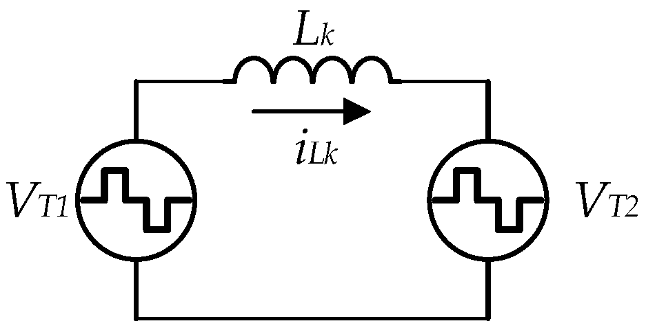
The way the DAB is analyzed is through the use of a simpler circuit, shown in Figure 2. The circuit comprises two square or semi-square voltage sources, VT1 and VT2, and an inductive element between them, Lk, named series inductance. This element is the transformer leakage inductance plus an added inductor in case of necessity. It is important to remark that the voltage VT1 is dependent on the input voltage vin and the voltage VT2 will correspond to the output voltage VOut multiplied by the transformer winding ratio, n.
In this case, the converter will be operated through a two-displacement angle modulation, and the operation is similar to DC-DC converters driven in discontinuous conduction mode (DCM).
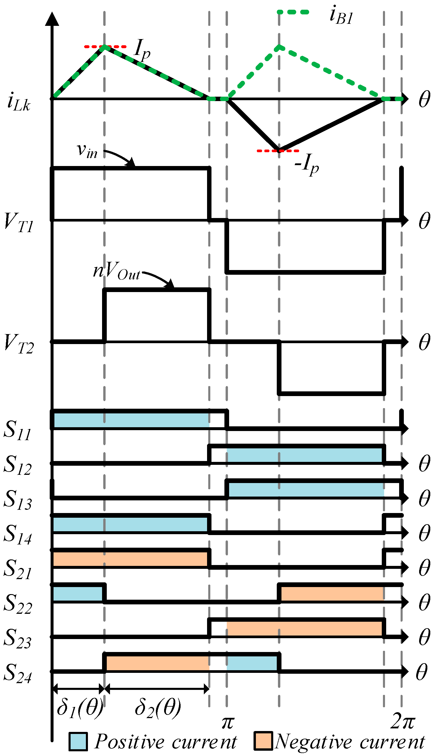
The DAB is operated in three stages per semi-cycle, as Figure 3 illustrates. This operation we called quasi-discontinuous conduction mode (QDCM), since it is similar to DC-DC conversion but is extrapolated for AC waveforms. This type of modulation has been used in [22] to improve performance, especially under light loads. Only one semi-cycle will be described, due to symmetry, which allows for determining the rectified series inductance average current.
The behavior is described as follows.
  • From 0 < θ < δ1: The voltage on the inductor is defined only by the input voltage, |vin|. The current will increase from zero to the peak current, IP.
  • From δ1 < θ < δ2: The series inductance current decreases from IP to zero due to the difference between the input voltage, |vin|, and the reflected output voltage, nVOut.
  • From δ2 < θ < π: The current will remain in the zero state. The output voltages of the primary side and secondary side inverters are zero.
The previous behavior is determined by:
i L k ( θ ) = { | v i n | ω L k θ 0 < θ δ 1 | v i n | n V O u t ω L k θ + | v i n | ω L k δ 1 0 < θ δ 2 0     0 < θ π δ 1 δ 2
where: |vin| is the rectified input voltage
  • nVOut is the output voltage multiplied by the transformer winding ratio,
  • Lk is the series inductance,
  • ω is the angular switching frequency,
  • δ1 is the charge displacement angle, and
  • δ2 is the discharge displacement angle.
As can be seen, in order to achieve the desired behavior, the reflected voltage, nVOut, must be greater than the rectified input voltage, |vin|, restricting the converter to operate in boosting mode. If this condition is not met, the current during the δ2 period will continue to increase. It is important to remark that, even though the converter is operating in boosting mode, is possible for the output voltage to be less than the input voltage, with the help of the transformer winding ratio.
In order to calculate the series inductance average current, first, the second displacement angle is referred to the first one by applying the volt-second technique to the inductor as follows:
| v i n | n V O u t ω L k δ 2 + | v i n | ω L k δ 1 = 0
Rearranging the terms, the second displacement angle is:
δ 2 = | v i n | n V O u t | v i n | δ 1
The rectified series inductance average current at high frequency might be found by using:
i B 1 ¯ ( θ ) = 1 π 0 π i L k d θ
Substituting (3) and solving (4) will result in the rectified series inductance average current.
i B 1 ¯ ( θ ) = δ 1 2 | v i n | 2 π ω L k [ n V O u t n V O u t | v i n | ]
Considering (5), the instantaneous power will be defined by the product of the average current at high frequency and the input voltage |vin|, resulting in:
P = δ 1 2 | v i n | 2 2 π ω L k [ n V O u t n V O u t | v i n | ]
By careful observation, it is noted in Figure 3 that the maximum value of the sum of the charge and discharge displacement angles is π, as illustrated by:
δ 1 + δ 2 π
Substituting (3) into (7), and reordering the next equation, it is obtained that:
δ 1 max π n V O u t | v i n | n V O u t
where δ1max is the maximum value that δ1 might have to maintain the QDCM operation.
Finally, by using (1) when θ = δ1, the peak current is calculated as:
I P = | v i n | ω L k δ 1

3. AC-DC DAB Behavior

3.1. Resistive Behavior

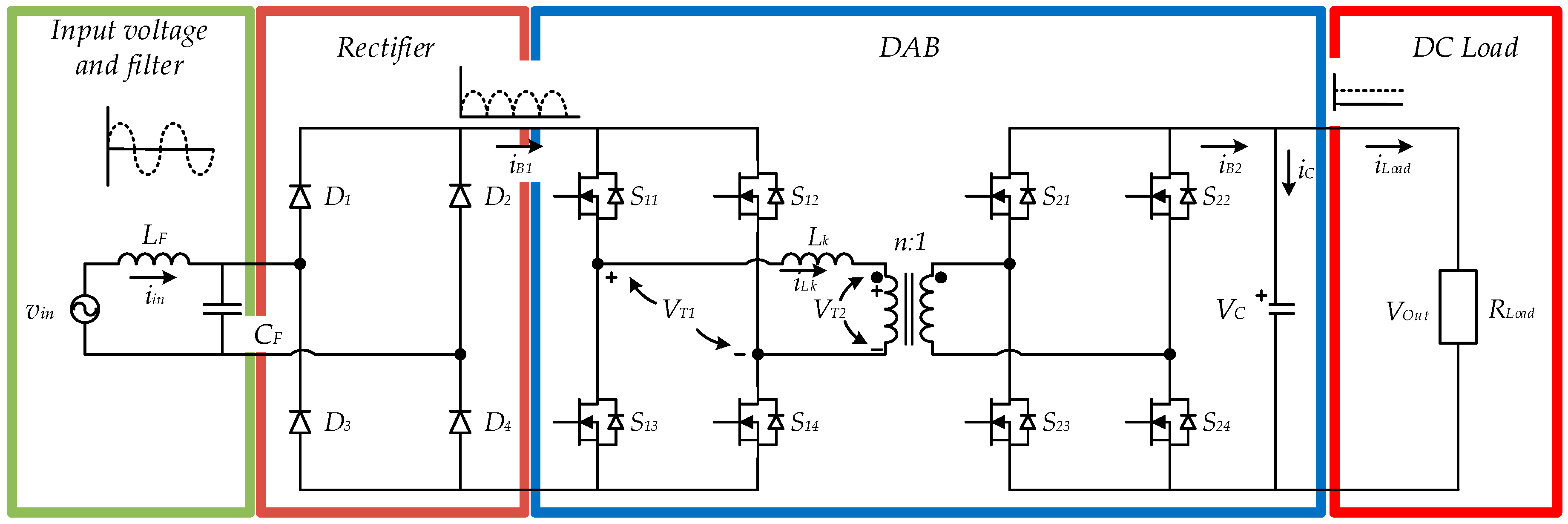
The AC-DC DAB converter, shown in Figure 4, comprises a rectifier stage and a DC-DC converter. The rectifier stage output is unfiltered; this means that the resultant voltage is the absolute value of the input AC voltage.
This configuration has been used in a full-bridge diode version [20], or for a synchronous operation [19]. The advantage of this converter is that there is only one controlled stage, making the converter more reliable and easier to implement. The idea behind the system is that the DAB will draw and shape the input current through the average value of the series inductance current.
In Figure 5, the current iB1 is the current being drawn by the DAB converter and the current iB2 is the DAB output current. To obtain the desired evolution, the DAB converter should operate as a resistive load—that is, iB1 should be proportional to the rectified AC mains.
The resistive load behavior is achieved through the correct variation of δ1 and δ2. This is achieved by utilizing (5). If (5) is carefully observed, it will be noted that there are several constant values, such as nVOut, ω, and Lk. If the average current iLk is desired to have the same waveform as the input voltage, δ1 must vary depending on the non-constant values of the equation.
Therefore, the input current for a resistive behavior is defined by:
i i n ¯ = | v i n | R e q
where R e q = 2 π ω L k ( n V O u t | v i n | ) δ 1 2 n V O u t .
As is seen from the resistance equivalency, the charge displacement angle δ1 must compensate for the difference between nVOut and vin to maintain the input current and voltage with a matching waveform. Therefore, the variation of δ1 is selected as:
δ 1 2 = k ( n V O u t | v i n | )
Solving δ1 from (11), it is obtained that:
δ 1 = k ( n V O u t | v i n | )
If (12) is substituted into (10), it can be noted that the input current will follow the input voltage, making the converter behave as a resistive load, achieving low input current THD and high-power factor.

3.2. Passive Element Design

To ensure that the converter operates properly, the series inductance and the output capacitor are essential. The worst-case scenario is used to design the elements and assure the desired signal behaviors.
In the case of the series inductance, (6) will be used. Considering the maximum value of |vin| = VP, where VP is the peak value of the input voltage, the maximum transferred power will be Pmax = 2P, which is the instantaneous power being transferred at the peak voltage and current. Substituting said parameters into (6), and rearranging terms, results in:
L k = δ 1 2 V P 2 4 π ω P [ n V O u t n V O u t V P ]
Considering the maximum displacement angle shown in (8), and substituting it into (13), results in the critical mode value for the series inductance current.
L k = π ( n V O u t V P ) V P 2 4 ω n P V O u t
This operation is not recommended, due to possible uncertainties caused by parasitic components when prototyping. Therefore, a security factor, 0.9 < kf < 0.95, is suggested to maintain the QDCM operation.
L k = k f π ( n V O u t V P ) V P 2 4 ω n P V O u t
In the case of the output capacitor, C, the high-frequency component coming from the DAB switching must be filtered; however, it features a low-frequency component, resulting in the rectified input. Considering the current iB2 from the DAB as:
i L k ( θ ) = { 0 0 < θ δ 1 | v i n | n V O u t ω L k θ + | v i n | ω L k δ 1 0 < θ δ 2 0     0 < θ π δ 1 δ 2
Averaging (16), and substituting (3), results in:
i B 2 ¯ = n 2 π ω L k [ ( | v i n | n V O u t ) δ 2 2 + 2 | v i n | δ 1 δ 2 ] = n δ 1 2 | v i n | 2 2 π ω L k ( n V O u t | v i n | )
Considering the value of the DAB equivalent resistance shown in (10), the DAB output current is obtained.
i B 2 ¯ = | v i n | 2 R e q V O u t
Substituting vin by VPsin(ωgt), the DAB output current results in:
i B 2 ¯ = V p 2 sin 2 ( ω g t ) V O u t R e q = V p 2 V O u t R e q [ 1 cos ( 2 ω g t ) ]
In (18) there is a DC component, represented by the unity, and an AC component, represented by the cosine. Considering that the capacitor will absorb the AC component when the DC component is at the load, the capacitor current is defined as:
i B 2 a c = i C = C d V O u t d t = V P 2 V O u t R e q cos ( 2 ω g t )
Finally, a volts per second analysis is performed, where the time differential equals the delta time and corresponds to the grid frequency multiplied by two, and the voltage differential is equal to the delta of the output voltage, which corresponds to the desired output voltage ripple. Considering that the minimum value of cos(2ωgt) = −1, the capacitor value depending on the desired ripple is obtained as.
C = V P 2 2 ω g R e q V O u t Δ V O u t
As is seen in (21), there exists a low-frequency component, represented by the ωg term. It is also noted that, due to the full-bridge diode rectifier operation, the frequency is double the AC mains frequency and, therefore, the capacitor value is reduced to half.
The input filter calculations were performed based on the Texas Instruments application note in [23].

3.3. Dynamical Modeling and Controller

In order to regulate the output voltage, a controller is required, and then a model. Considering the power equivalency in (22), the model is obtained:
P C = P i n P O
Substituting the voltage and resistance equivalencies, it is obtained that:
v O u t C d v O u t d t = V P 2 2 R e q v O u t 2 R
where: PC is the capacitor power.
  • Pin is the input power,
  • PO is the output power, and
  • R is the load.
It is noted that the DAB equivalent resistive behavior is used for the input power calculation.
Linearizing (23) around the operating point, solving for the derivative expression, using the Req value equivalency, and applying the partial derivative with respect δ1 and vOut, it is obtained that:
d v O u t d t = [ n 2 D 1 2 V P 2 4 π ω L k C ( n V O u t V P ) 2 + 1 R C ] v O u t + n D 1 V P 2 2 π ω L k C ( n V O u t V P ) δ 1
where D1 is the charge displacement angle at the operating point.
Rearranging the terms in (23), the output voltage transfer function is obtained as:
v O u t δ 1 = A [ s + A n D 1 ( n V O u t V P ) + 1 R C ]
where: A = n D 1 V P 2 2 π ω L k C ( n V O u t V P ) .
As is seen from (25), the system features a first-order behavior; therefore, a simple controller might be used for regulating the output voltage.
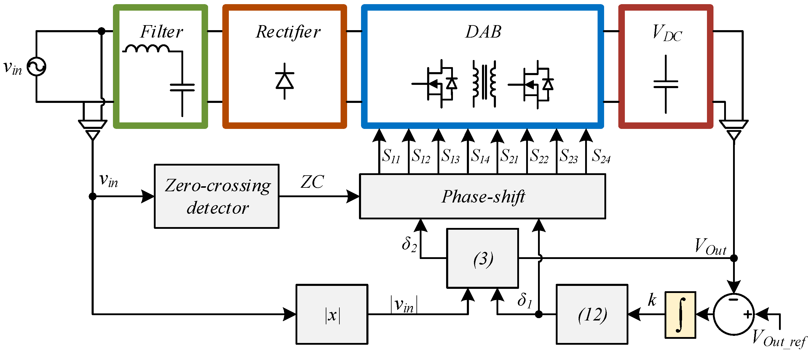
In Figure 6, the control scheme is proposed. From the figure, it is observed that the use of an integrator delivers the variable k, to regulate the value of δ1, by using (12), and (3), to calculate δ2.
Using the parameters shown in Table 1, a frequency response behavior might be established. In Figure 7, for the system open loop and the closed loop, considering an integrator, frequency responses are illustrated. The open loop shows a low-pass filter behavior, while the closed loop depicts high DC gain, reducing the steady-state error, and a small bandwidth, keeping the value k as constant as possible during a grid semi-cycle.

4. Experimental Results

Considering the parameters shown in Table 1, an experimental setup with C3M0065090D MOSFETs and MUR1560 diodes, shown in Figure 8, was tested. A GPIC 9683 was used to generate the activation signals required for the prototype.
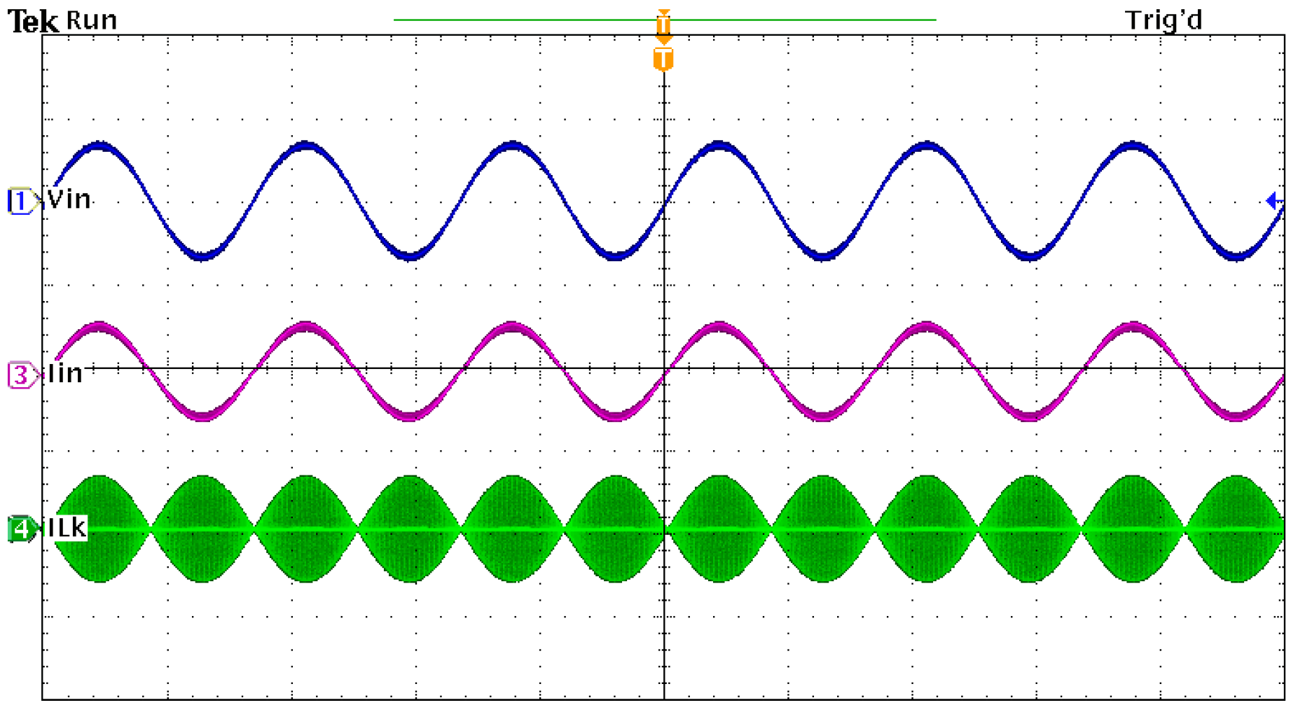
In Figure 9, the input voltage, the input current, and the series inductance current of the DAB converter are shown, when operating at nominal voltage and observing the low-frequency behavior. It is noted that the power factor is high, because the input current, as well as the input voltage, are in phase.
In Figure 10, high-frequency signals are observed. The voltage VT1, the voltage VT2/n, and the series inductance current are displayed in the oscillogram. The expected behavior of charge and discharge is generated.
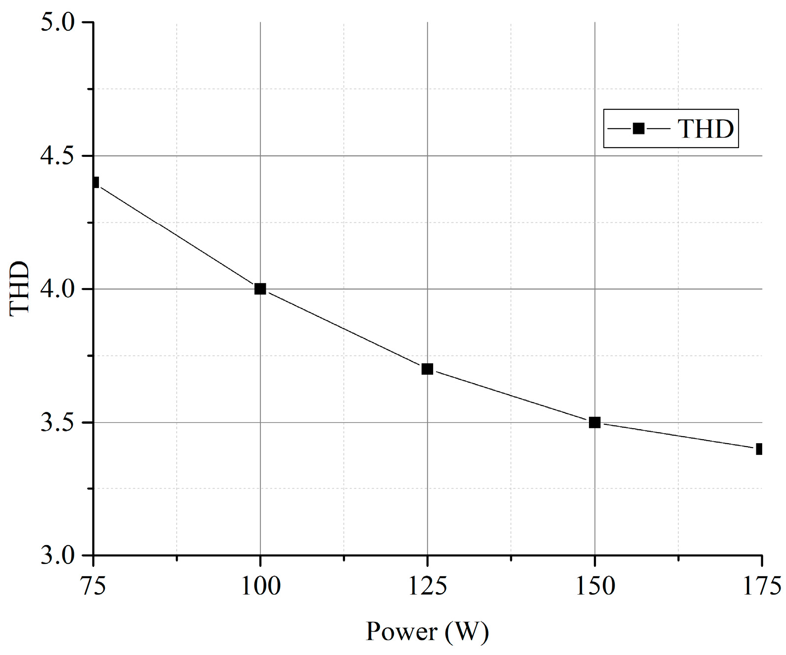
From Figure 9, it is seen that the input current features low THD. Considering the IEEE 519-2014 standard [24], a grid-connected device to an AC mains with an amplitude of less than 1 kV must have a THD current below 8%, as is illustrated in Figure 11, which presents the THD evolution in comparison with a power sweep.
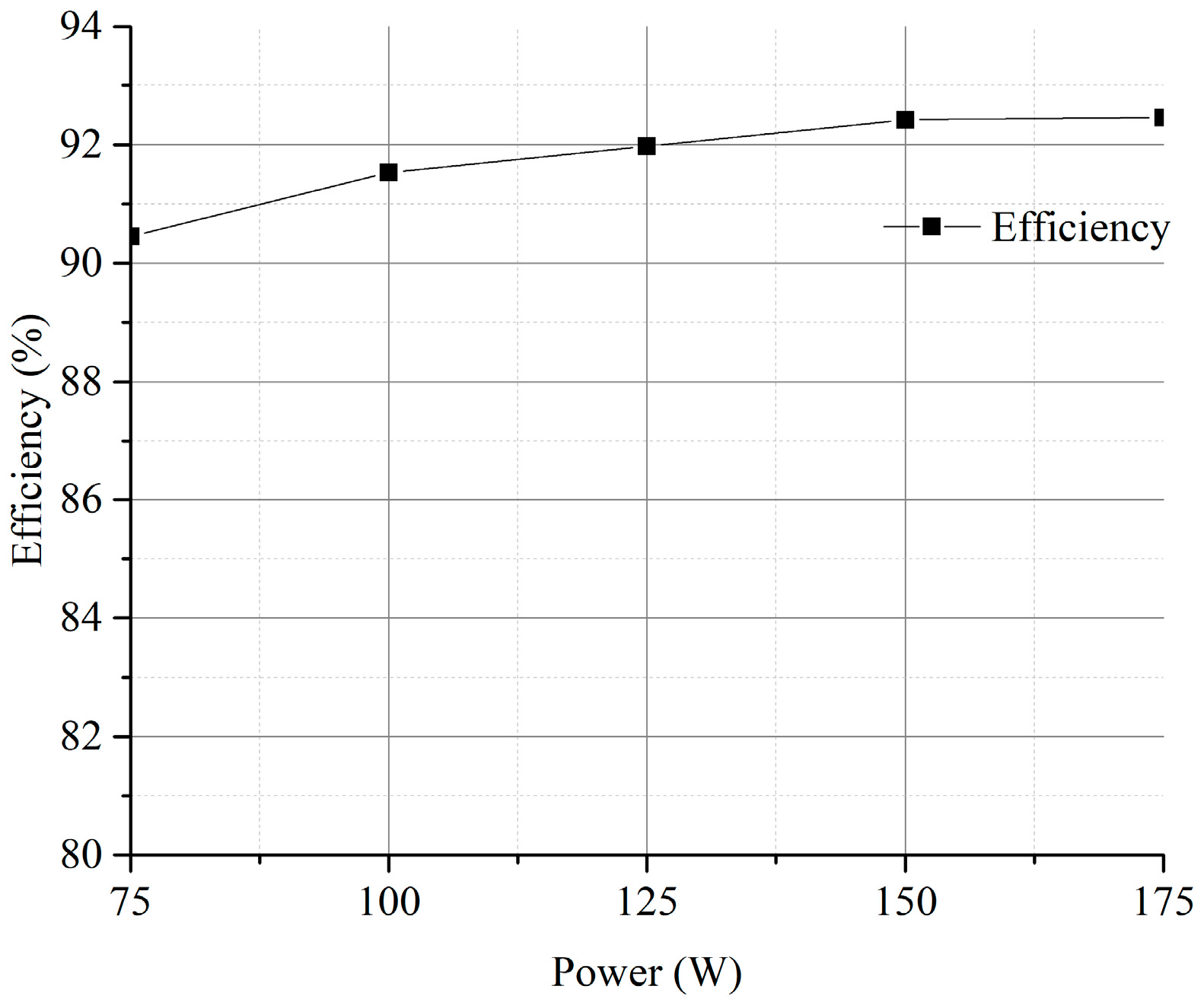
The efficiency, in comparison with the power, is observed in Figure 12. A peak efficiency of 92.5% is achieved; however, at light load, efficiency still surpasses 90% efficiency.
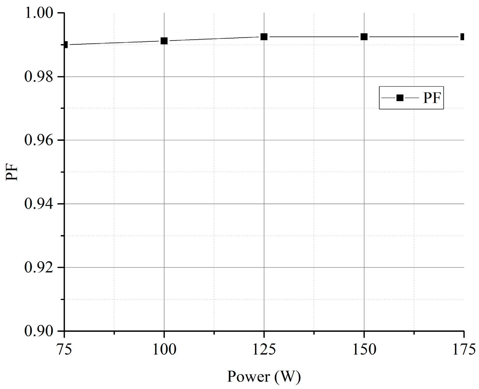
Finally, the power factor through a power sweep is depicted in Figure 13. As is observed, the power factor is almost at unity during the whole operation.
It is important to remark that measurements were perfomed using the Chroma 66,204 power meter.

5. Conclusions

In this paper, an AC-DC DAB converter is used. The system, comprised of two stages, uses a full-bridge diode rectifier and a DC-DC DAB converter. The use of only one controlled stage makes the system easier to implement and more reliable.
The modulation makes the DC-DC converter behave as a resistor, as shown in Section 3, achieving a low input current THD and a high power factor in an easy manner. The DAB converter draws and shapes the input current through the average value of the series inductance current. The output capacitor filters the high-frequency component coming from the DAB switching, and the low-frequency component which originates from the rectified AC voltage.
The system might be seen as a capacitor being fed with the current coming from the DAB. This is reflected directly in the dynamical equations. A first-order system depicts the behavior of the converter.
A low-power prototype was tested to corroborate that the proposal is working. The input current THD is within the IEEE 519-2014 standard, while the power factor is almost at unity through a power sweep. The efficiency is better than some similar systems while maintaining simplicity in the implementation.

Author Contributions

Methodology, R.O.; Validation, P.G.; Investigation, P.G.; Resources, M.L.; Writing–review & editing, N.V. and J.V.; Supervision, M.L.; Funding acquisition, N.V., R.O. and C.H. All authors have read and agreed to the published version of the manuscript.

Funding

This work was sponsored by TecNM under project No. 13737.22-P.

Data Availability Statement

All the information is in this work.

Conflicts of Interest

The authors declare no conflict of interest.

References

  1. Von Baeckman, W.; Schwenk, W.; Prinz, W. Handbook of Cathodic Protection. Theory and Practice of Electrochemical Protection Process, 3rd ed.; Elsevier: Amsterdam, The Netherlands, 1997; pp. 225–242. [Google Scholar]
  2. Ortiz-Castrillón, J.R.; Mejía-Ruíz, G.E.; Muñoz-Galeano, N.; López-Lezama, J.M.; Saldarriaga-Zuluaga, S.D. PFC Single-Phase AC/DC Boost Converters: Bridge, Semi-Bridgeless, and Bridgeless Topologies. Appl. Sci. 2021, 11, 7651. [Google Scholar] [CrossRef]
  3. De Doncker, R.W.; Divan, D.M.; Kheraluwala, M.H. A three-phase soft-switched high power density DC/DC converter for high power applications. IEEE Trans. Ind. Appl. 1991, 27, 63–73. [Google Scholar] [CrossRef]
  4. Rodríguez, A.; Vázquez, A.; Lamar, D.G.; Hernando, M.M.; Sebastián, J. Different Purpose Design Strategies and Techniques to Improve the Performance of a Dual Active Bridge with Phase-Shift Control. IEEE Trans. Power Electron. 2014, 30, 790–804. [Google Scholar] [CrossRef]
  5. Falcones, S.; Ayyanar, R.; Mao, X. A DC-DC Multiport-Converter-Based Solid-State Transformer Integrating Distributed Generation and Storage. IEEE Trans. Power Electron. 2012, 28, 2192–2203. [Google Scholar] [CrossRef]
  6. Ferreira Costa, L.; De Carne, G.; Buticchi, G.; Liserre, M. The Smart Transformer: A solid-state transformer tailored to provide ancillary services to the distribution grid. IEEE Power Electron. Mag. 2017, 4, 56–67. [Google Scholar] [CrossRef] [Green Version]
  7. Syed, I.; Khadkikar, V. Replacing the Grid Interface Transformer in Wind Energy Conversion System with Solid-State Transformer. IEEE Trans. Power Syst. 2016, 32, 2152–2160. [Google Scholar] [CrossRef]
  8. Madhusoodhanan, S.; Tripathi, A.; Patel, D.; Mainali, K.; Kadavelugu, A.; Hazra, S.; Bhattacharya, S.; Hatua, K. Solid-State Transformer and MV Grid Tie Applications Enabled by 15 kV SiC IGBTs and 10 kV SiC MOSFETs Based Multilevel Converters. IEEE Trans. Ind. Appl. 2015, 51, 3343–3360. [Google Scholar] [CrossRef]
  9. Buticchi, G.; Costa, L.F.; Barater, D.; Liserre, M.; Dominguez, E. A Quadruple Active Bridge Converter for the Storage Integration on the More Electric Aircraft. IEEE Trans. Power Electron. 2017, 33, 8174–8186. [Google Scholar] [CrossRef] [Green Version]
  10. Zhu, R.; De Carne, G.; Deng, F.; Liserre, M. Integration of large photovoltaic and wind system by means of smart transformer. IEEE Trans. Ind. Electron. 2017, 64, 8928–8938. [Google Scholar] [CrossRef] [Green Version]
  11. Guan, M. A Series-Connected Offshore Wind Farm Based on Modular Dual-Active-Bridge (DAB) Isolated DC-DC Converter. IEEE Trans. Energy Convers. 2019, 34, 1422–1431. [Google Scholar] [CrossRef]
  12. Zhou, H.; Khambadkone, A.M. Hybrid Modulation for Dual-Active-Bridge Bidirectional Converter with Extended Power Range for Ultracapacitor Application. In Proceedings of the 2008 IEEE Industry Applications Society Annual Meeting, Edmonton, AB, Canada, 5–9 October 2008. [Google Scholar]
  13. Inoue, S.; Akagi, H. A Bidirectional DC-DC Converter for an Energy Storage System with Galvanic Isolation. IEEE Trans. Power Electron. 2007, 22, 2299–2306. [Google Scholar] [CrossRef]
  14. An, F.; Song, W.; Yang, K.; Yang, S.; Ma, L. A Simple Power Estimation with Triple Phase-Shift Control for the Output Parallel DAB DC-DC Converters in Power Electronic Traction Transformer for Railway Locomotive Application. IEEE Trans. Transp. Electrif. 2018, 5, 299–310. [Google Scholar] [CrossRef]
  15. Hou, N.; Li, Y.W. Overview and Comparison of Modulation and Control Strategies for a Nonresonant Single-Phase Dual-Active-Bridge DC-DC Converter. IEEE Trans. Power Electron. 2019, 35, 3148–3172. [Google Scholar] [CrossRef]
  16. Vazquez, N.; Liserre, M. Peak Current Control and Feed-Forward Compensation of a DAB Converter. IEEE Trans. Ind. Electron. 2019, 67, 8381–8391. [Google Scholar] [CrossRef]
  17. Zengin, S.; Boztepe, M. Modified dual active bridge photovoltaic inverter for solid state transformer applications. In Proceedings of the 2014 International Symposium on Fundamentals of Electrical Engineering (ISFEE), Bucharest, Romania, 28–29 November 2014. [Google Scholar]
  18. Zengin, S.; Boztepe, M. Bi-directional DCM DAB inverter for SST applications. In Proceedings of the 2014 International Symposium on Fundamentals of Electrical Engineering (ISFEE), Bucharest, Romania, 28–29 November 2014. [Google Scholar]
  19. Zengin, S.; Boztepe, M. A Novel Current Modulation Method to Eliminate Low-Frequency Harmonics in Single-Stage Dual Active Bridge AC-DC Converter. IEEE Trans. Ind. Electron. 2019, 67, 1048–1058. [Google Scholar] [CrossRef]
  20. Sha, D.; Wang, S. A Single-Stage Natural Power Factor Corrector Based on Dual Active Bridge DC-DC Converter Without Inner Current Tracking Loop. IEEE Trans. Power Electron. 2020, 36, 342–352. [Google Scholar] [CrossRef]
  21. Everts, J.; Krismer, F.; Van den Keybus, J.; Driesen, J.; Kolar, J.W. Optimal ZVS Modulation of Single-Phase Single-Stage Bidirectional DAB AC-DC Converters. IEEE Trans. Power Electron. 2013, 29, 3954–3970. [Google Scholar] [CrossRef] [Green Version]
  22. Gu, Q.; Yuan, L.; Nie, J.; Sun, J.; Zhao, Z. Current Stress Minimization of Dual-Active-Bridge DC-DC Converter Within the Whole Operating Range. IEEE J. Emerg. Sel. Top. Power Electron. 2018, 7, 129–142. [Google Scholar] [CrossRef]
  23. Input Filter Design for Switching Power Supplies, Texas Instruments SNVA538. 2010. Available online: https://www.ti.com/lit/an/snva538/snva538.pdf (accessed on 1 July 2022).
  24. IEEE Recommended Practice and Requirements for Harmonic Control in Electric Power Systems, IEEE Std 519-2014. June 2014. Available online: https://standards.ieee.org/ieee/519/3710/ (accessed on 1 July 2022).
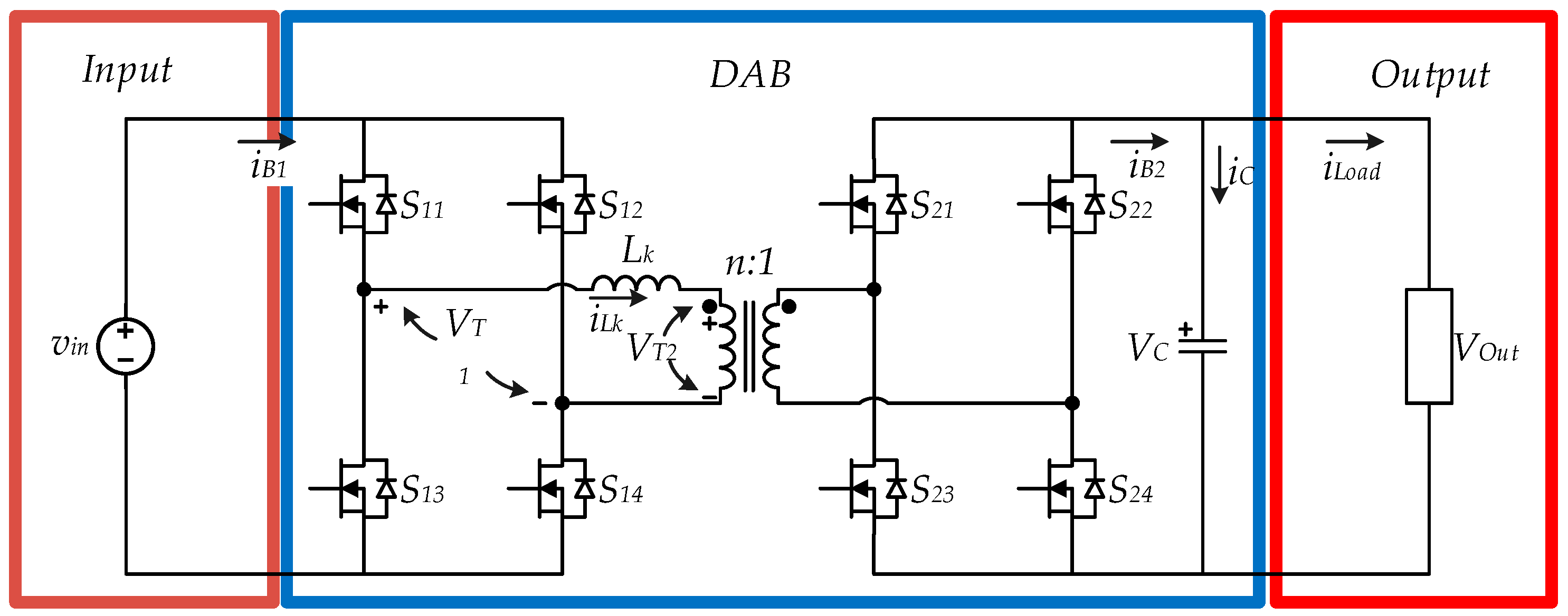
Figure 1. DAB schematic.
Energies 16 00320 g001
Figure 2. Converter simplified circuit intended for analysis.
Energies 16 00320 g002
Figure 3. Boost QDCM waveforms. From top to bottom, series inductance current, primary-side inverter output voltage, reflected secondary-side inverter output voltage, and switch activation signals with their respective negated complementary pulses.
Energies 16 00320 g003
Figure 4. Proposed AC-DC DAB system.
Energies 16 00320 g004
Figure 5. DAB input and output currents evolution with the rectified input voltage. In black rectified ac mains, in blue is the current of rectified ac mains, and in orange is the rectified secondary current of the DAB.
Energies 16 00320 g005
Figure 6. Proposed controller.
Energies 16 00320 g006
Figure 7. System frequency response in open loop and closed loop.
Energies 16 00320 g007
Figure 8. Prototype photograph.
Energies 16 00320 g008
Figure 9. Low-frequency signals of the AC-DC DAB converter. From top to bottom, input voltage (250 V/div), input current (5 A/div), and DAB series inductance current (25 A/div).
Energies 16 00320 g009
Figure 10. High-frequency signals. From top to bottom, voltage VT1 (250 V/div), voltage VT2/n (250 V/div), and series inductance current (10 A/div).
Energies 16 00320 g010
Figure 11. THD evolution through a power sweep.
Energies 16 00320 g011
Figure 12. AC-DC DAB efficiency versus output power.
Energies 16 00320 g012
Figure 13. System power factor vs. output power.
Energies 16 00320 g013
Table 1. AC-DC DAB test parameters.
ParameterValue
Output power (P)175 W
Input voltage (vin)90 VRMS, 60 Hz
Output voltage (VOut)200 V
Switching frequency (ω)30 kHz
Series inductance (Lk)83 μH
Transformer winding ratio (n)1
Output capacitor (C)1000 μF
Filter inductor (LF)500 μH
Filter capacitor (CF)2 μF
Disclaimer/Publisher’s Note: The statements, opinions and data contained in all publications are solely those of the individual author(s) and contributor(s) and not of MDPI and/or the editor(s). MDPI and/or the editor(s) disclaim responsibility for any injury to people or property resulting from any ideas, methods, instructions or products referred to in the content.