

AC-DC DAB Converter with Power Factor Correction
 ,
,  and
and
Abstract
:1. Introduction
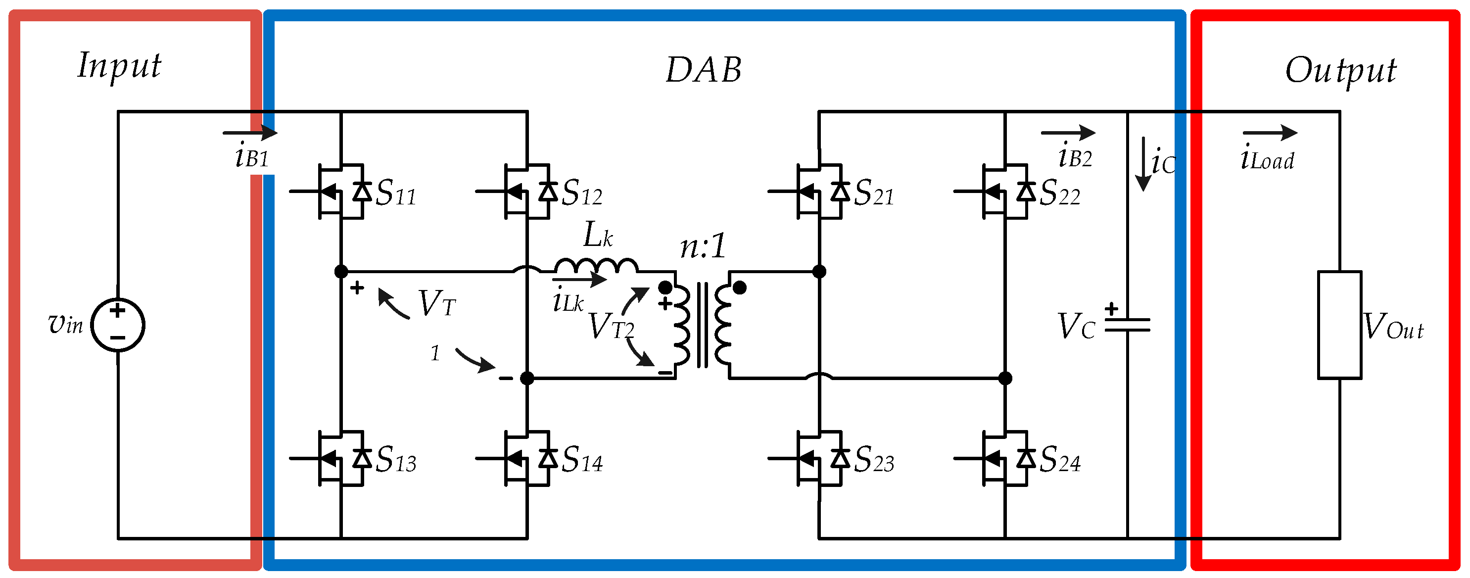
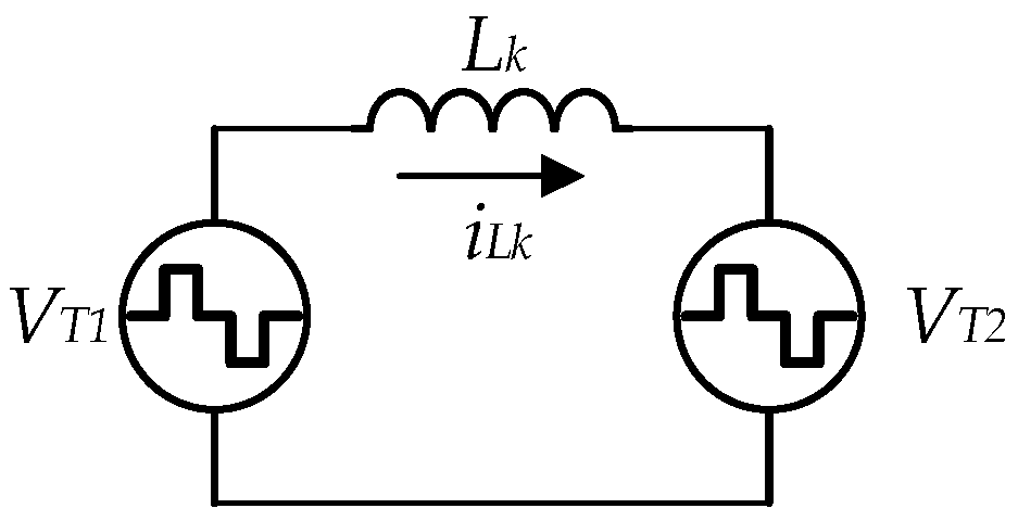
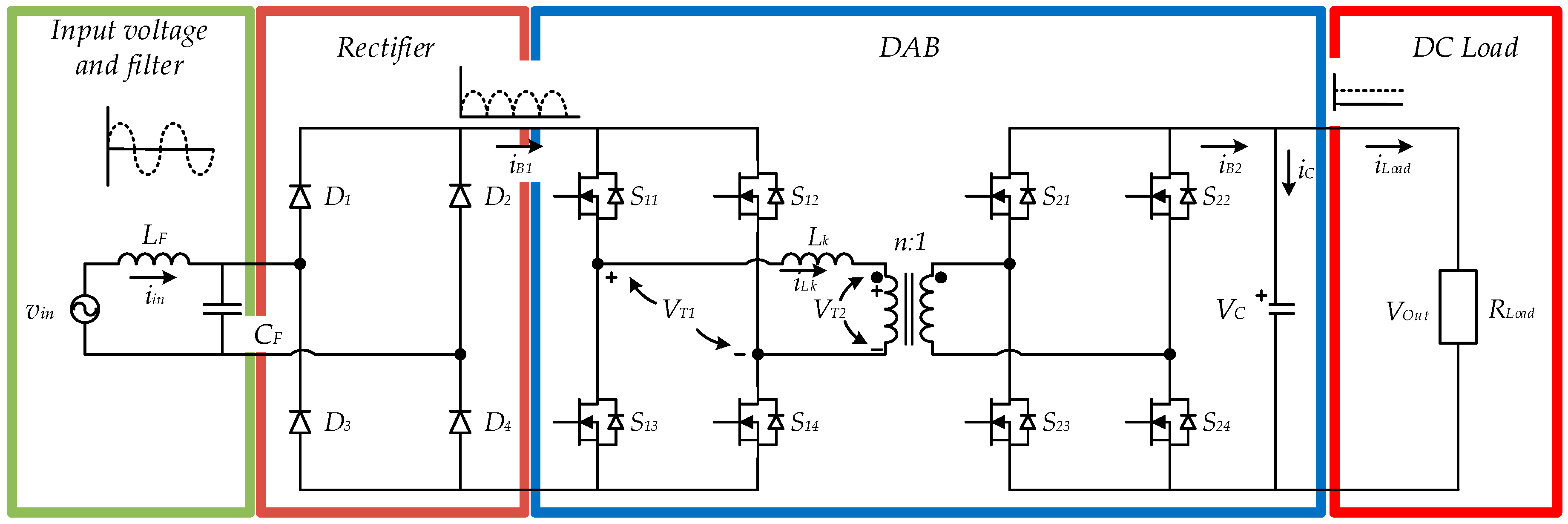
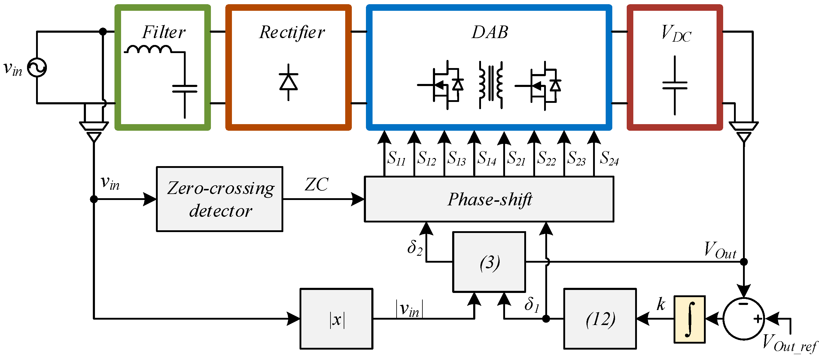
2. DAB Converter
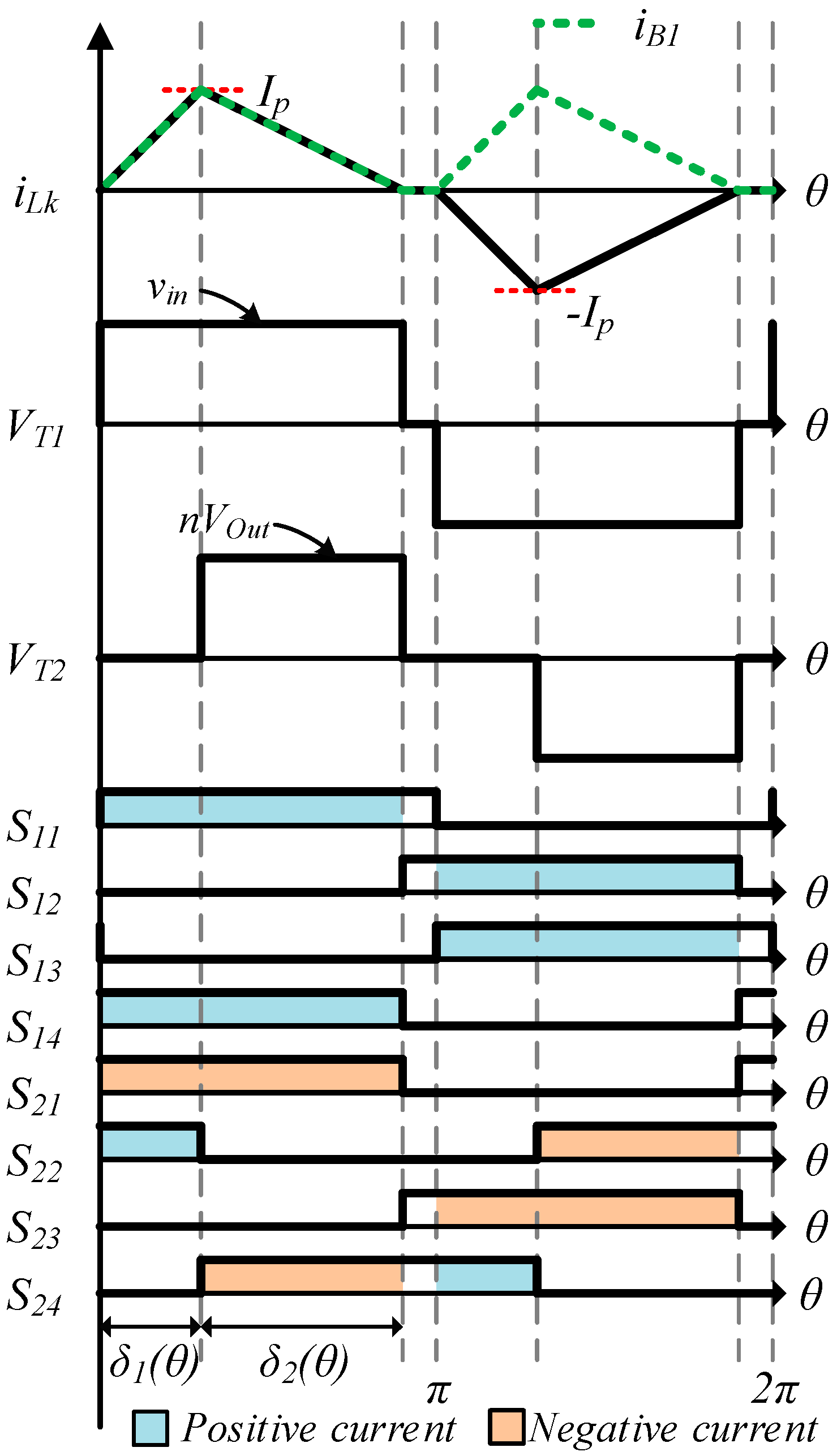
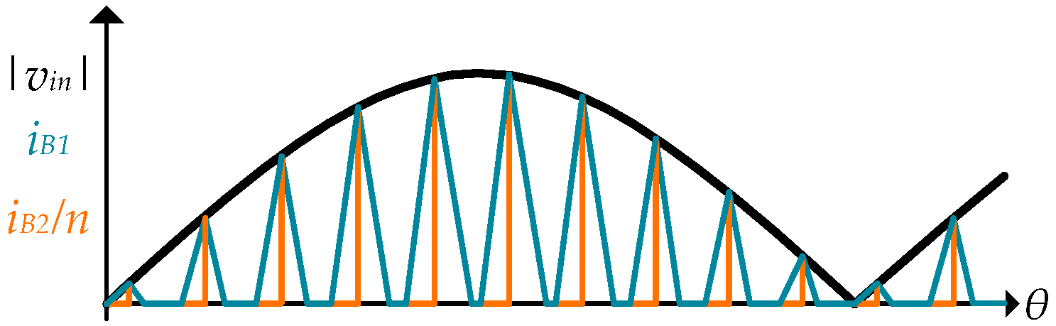
- From 0 < θ < δ1: The voltage on the inductor is defined only by the input voltage, |vin|. The current will increase from zero to the peak current, IP.
- From δ1 < θ < δ2: The series inductance current decreases from IP to zero due to the difference between the input voltage, |vin|, and the reflected output voltage, nVOut.
- From δ2 < θ < π: The current will remain in the zero state. The output voltages of the primary side and secondary side inverters are zero.
- nVOut is the output voltage multiplied by the transformer winding ratio,
- Lk is the series inductance,
- ω is the angular switching frequency,
- δ1 is the charge displacement angle, and
- δ2 is the discharge displacement angle.
3. AC-DC DAB Behavior
3.1. Resistive Behavior
3.2. Passive Element Design
3.3. Dynamical Modeling and Controller
- Pin is the input power,
- PO is the output power, and
- R is the load.
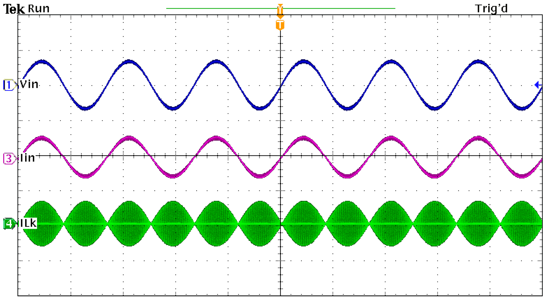
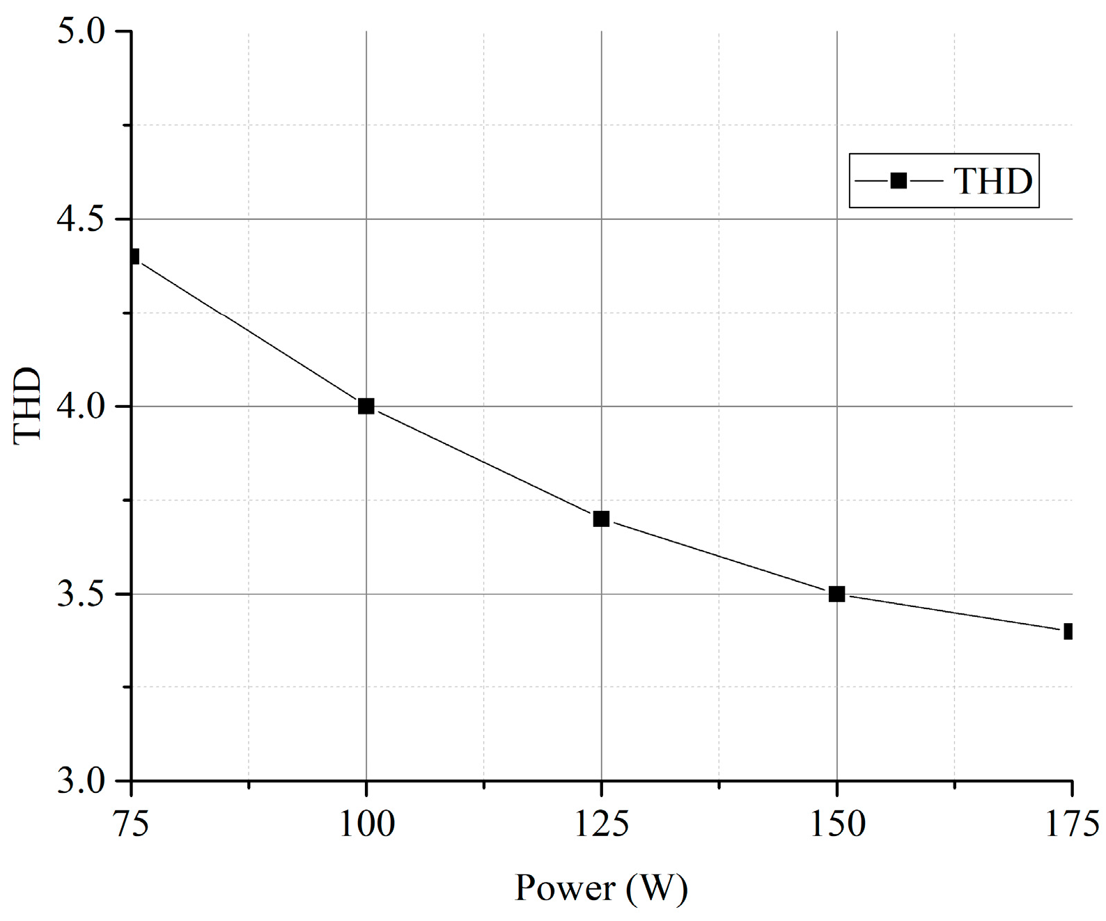
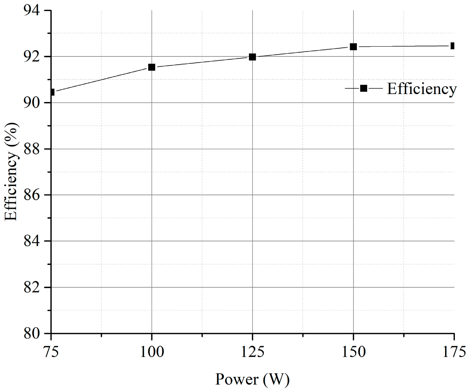
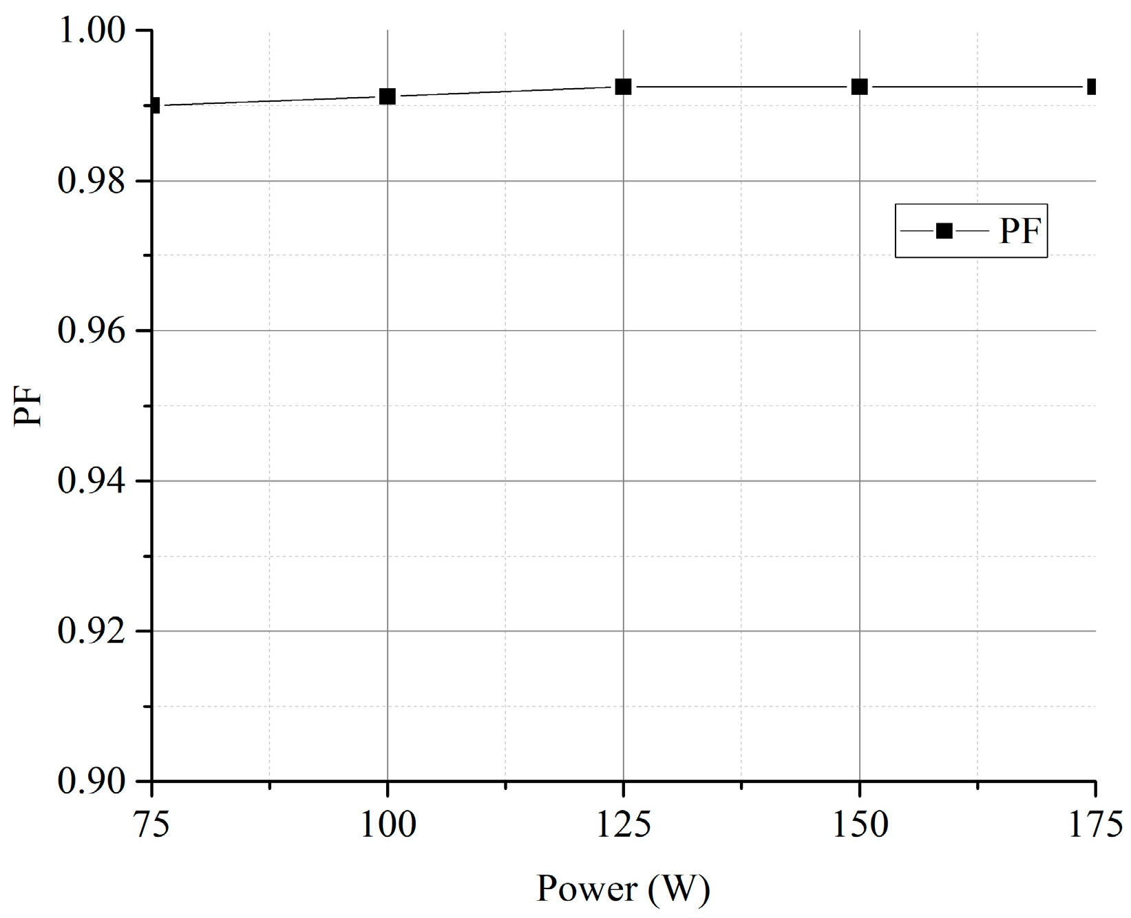
4. Experimental Results
5. Conclusions
Author Contributions
Funding
Data Availability Statement
Conflicts of Interest
References
- Von Baeckman, W.; Schwenk, W.; Prinz, W. Handbook of Cathodic Protection. Theory and Practice of Electrochemical Protection Process, 3rd ed.; Elsevier: Amsterdam, The Netherlands, 1997; pp. 225–242. [Google Scholar]
- Ortiz-Castrillón, J.R.; Mejía-Ruíz, G.E.; Muñoz-Galeano, N.; López-Lezama, J.M.; Saldarriaga-Zuluaga, S.D. PFC Single-Phase AC/DC Boost Converters: Bridge, Semi-Bridgeless, and Bridgeless Topologies. Appl. Sci. 2021, 11, 7651. [Google Scholar] [CrossRef]
- De Doncker, R.W.; Divan, D.M.; Kheraluwala, M.H. A three-phase soft-switched high power density DC/DC converter for high power applications. IEEE Trans. Ind. Appl. 1991, 27, 63–73. [Google Scholar] [CrossRef]
- Rodríguez, A.; Vázquez, A.; Lamar, D.G.; Hernando, M.M.; Sebastián, J. Different Purpose Design Strategies and Techniques to Improve the Performance of a Dual Active Bridge with Phase-Shift Control. IEEE Trans. Power Electron. 2014, 30, 790–804. [Google Scholar] [CrossRef]
- Falcones, S.; Ayyanar, R.; Mao, X. A DC-DC Multiport-Converter-Based Solid-State Transformer Integrating Distributed Generation and Storage. IEEE Trans. Power Electron. 2012, 28, 2192–2203. [Google Scholar] [CrossRef]
- Ferreira Costa, L.; De Carne, G.; Buticchi, G.; Liserre, M. The Smart Transformer: A solid-state transformer tailored to provide ancillary services to the distribution grid. IEEE Power Electron. Mag. 2017, 4, 56–67. [Google Scholar] [CrossRef] [Green Version]
- Syed, I.; Khadkikar, V. Replacing the Grid Interface Transformer in Wind Energy Conversion System with Solid-State Transformer. IEEE Trans. Power Syst. 2016, 32, 2152–2160. [Google Scholar] [CrossRef]
- Madhusoodhanan, S.; Tripathi, A.; Patel, D.; Mainali, K.; Kadavelugu, A.; Hazra, S.; Bhattacharya, S.; Hatua, K. Solid-State Transformer and MV Grid Tie Applications Enabled by 15 kV SiC IGBTs and 10 kV SiC MOSFETs Based Multilevel Converters. IEEE Trans. Ind. Appl. 2015, 51, 3343–3360. [Google Scholar] [CrossRef]
- Buticchi, G.; Costa, L.F.; Barater, D.; Liserre, M.; Dominguez, E. A Quadruple Active Bridge Converter for the Storage Integration on the More Electric Aircraft. IEEE Trans. Power Electron. 2017, 33, 8174–8186. [Google Scholar] [CrossRef] [Green Version]
- Zhu, R.; De Carne, G.; Deng, F.; Liserre, M. Integration of large photovoltaic and wind system by means of smart transformer. IEEE Trans. Ind. Electron. 2017, 64, 8928–8938. [Google Scholar] [CrossRef] [Green Version]
- Guan, M. A Series-Connected Offshore Wind Farm Based on Modular Dual-Active-Bridge (DAB) Isolated DC-DC Converter. IEEE Trans. Energy Convers. 2019, 34, 1422–1431. [Google Scholar] [CrossRef]
- Zhou, H.; Khambadkone, A.M. Hybrid Modulation for Dual-Active-Bridge Bidirectional Converter with Extended Power Range for Ultracapacitor Application. In Proceedings of the 2008 IEEE Industry Applications Society Annual Meeting, Edmonton, AB, Canada, 5–9 October 2008. [Google Scholar]
- Inoue, S.; Akagi, H. A Bidirectional DC-DC Converter for an Energy Storage System with Galvanic Isolation. IEEE Trans. Power Electron. 2007, 22, 2299–2306. [Google Scholar] [CrossRef]
- An, F.; Song, W.; Yang, K.; Yang, S.; Ma, L. A Simple Power Estimation with Triple Phase-Shift Control for the Output Parallel DAB DC-DC Converters in Power Electronic Traction Transformer for Railway Locomotive Application. IEEE Trans. Transp. Electrif. 2018, 5, 299–310. [Google Scholar] [CrossRef]
- Hou, N.; Li, Y.W. Overview and Comparison of Modulation and Control Strategies for a Nonresonant Single-Phase Dual-Active-Bridge DC-DC Converter. IEEE Trans. Power Electron. 2019, 35, 3148–3172. [Google Scholar] [CrossRef]
- Vazquez, N.; Liserre, M. Peak Current Control and Feed-Forward Compensation of a DAB Converter. IEEE Trans. Ind. Electron. 2019, 67, 8381–8391. [Google Scholar] [CrossRef]
- Zengin, S.; Boztepe, M. Modified dual active bridge photovoltaic inverter for solid state transformer applications. In Proceedings of the 2014 International Symposium on Fundamentals of Electrical Engineering (ISFEE), Bucharest, Romania, 28–29 November 2014. [Google Scholar]
- Zengin, S.; Boztepe, M. Bi-directional DCM DAB inverter for SST applications. In Proceedings of the 2014 International Symposium on Fundamentals of Electrical Engineering (ISFEE), Bucharest, Romania, 28–29 November 2014. [Google Scholar]
- Zengin, S.; Boztepe, M. A Novel Current Modulation Method to Eliminate Low-Frequency Harmonics in Single-Stage Dual Active Bridge AC-DC Converter. IEEE Trans. Ind. Electron. 2019, 67, 1048–1058. [Google Scholar] [CrossRef]
- Sha, D.; Wang, S. A Single-Stage Natural Power Factor Corrector Based on Dual Active Bridge DC-DC Converter Without Inner Current Tracking Loop. IEEE Trans. Power Electron. 2020, 36, 342–352. [Google Scholar] [CrossRef]
- Everts, J.; Krismer, F.; Van den Keybus, J.; Driesen, J.; Kolar, J.W. Optimal ZVS Modulation of Single-Phase Single-Stage Bidirectional DAB AC-DC Converters. IEEE Trans. Power Electron. 2013, 29, 3954–3970. [Google Scholar] [CrossRef] [Green Version]
- Gu, Q.; Yuan, L.; Nie, J.; Sun, J.; Zhao, Z. Current Stress Minimization of Dual-Active-Bridge DC-DC Converter Within the Whole Operating Range. IEEE J. Emerg. Sel. Top. Power Electron. 2018, 7, 129–142. [Google Scholar] [CrossRef]
- Input Filter Design for Switching Power Supplies, Texas Instruments SNVA538. 2010. Available online: https://www.ti.com/lit/an/snva538/snva538.pdf (accessed on 1 July 2022).
- IEEE Recommended Practice and Requirements for Harmonic Control in Electric Power Systems, IEEE Std 519-2014. June 2014. Available online: https://standards.ieee.org/ieee/519/3710/ (accessed on 1 July 2022).


| Parameter | Value |
|---|---|
| Output power (P) | 175 W |
| Input voltage (vin) | 90 VRMS, 60 Hz |
| Output voltage (VOut) | 200 V |
| Switching frequency (ω) | 30 kHz |
| Series inductance (Lk) | 83 μH |
| Transformer winding ratio (n) | 1 |
| Output capacitor (C) | 1000 μF |
| Filter inductor (LF) | 500 μH |
| Filter capacitor (CF) | 2 μF |
Disclaimer/Publisher’s Note: The statements, opinions and data contained in all publications are solely those of the individual author(s) and contributor(s) and not of MDPI and/or the editor(s). MDPI and/or the editor(s) disclaim responsibility for any injury to people or property resulting from any ideas, methods, instructions or products referred to in the content. |
© 2022 by the authors. Licensee MDPI, Basel, Switzerland. This article is an open access article distributed under the terms and conditions of the Creative Commons Attribution (CC BY) license (https://creativecommons.org/licenses/by/4.0/).
Share and Cite
Guzmán, P.; Vázquez, N.; Liserre, M.; Orosco, R.; Vaquero, J.; Hernández, C. AC-DC DAB Converter with Power Factor Correction. Energies 2023, 16, 320. https://doi.org/10.3390/en16010320
Guzmán P, Vázquez N, Liserre M, Orosco R, Vaquero J, Hernández C. AC-DC DAB Converter with Power Factor Correction. Energies. 2023; 16(1):320. https://doi.org/10.3390/en16010320
Chicago/Turabian StyleGuzmán, Pablo, Nimrod Vázquez, Marco Liserre, Rodolfo Orosco, Joaquín Vaquero, and Claudia Hernández. 2023. "AC-DC DAB Converter with Power Factor Correction" Energies 16, no. 1: 320. https://doi.org/10.3390/en16010320