Article

High Step-Up Three-Level Soft Switching DC-DC Converter for Photovoltaic Generation Systems

by
Seyed Shahriyar Taghavi
1,
Mahdi Rezvanyvardom
1,
Amin Mirzaei
1 and
Saman A. Gorji
2,3,*
1
Department of Electrical Engineering, Faculty of Engineering, Arak University, Arak 3848-7-6941, Iran
2
Centre for Clean Energy Technologies and Practices, Queensland University of Technology, Brisbane, QLD 4000, Australia
3
Centre for Smart Power and Energy Research, School of Engineering, Deakin University, Waurn Ponds, Geelong, VIC 3216, Australia
*
Author to whom correspondence should be addressed.
Energies 2023, 16(1), 41; https://doi.org/10.3390/en16010041
Submission received: 28 November 2022 / Revised: 12 December 2022 / Accepted: 18 December 2022 / Published: 21 December 2022
(This article belongs to the Special Issue Design and Application of DC-DC Converters in Power Systems)

Abstract

:
In this paper, a high step-up three-level DC–DC converter with a symmetric structure for PV application is proposed. The converter has high voltage gain. This is achieved due to the use of two high step-up cells and two resonant paths in its structure. The converter has low input current ripples and the voltage stress across all switches is equal to half of the output voltage. The proposed converter uses simple pulse–width modulation (PWM) to trigger the switches. Hence, the proposed converter benefits from a simple structure and control circuit. All semiconductor devices are turned on/off under ZCS conditions. Thus, the switching losses are decreased, and the total efficiency is increased. The converter is implemented and tested through a laboratory prototype. The experimental results verify the theoretical analysis.

1. Introduction

The demand for photovoltaic (PV) power generation has increased significantly in recent years. Many reasons are effective to reach this aim, such as the reduction of PV cost and increment of PV power generation capacity. In addition, global warming and environmental pollution are other important reasons that have forced different countries to use renewable energy sources, especially PV to generate electricity instead of using fossil fuels [1,2]. In a grid-connected PV system, the voltage level, which is generated by PV arrays, cannot be used to feed the grid-connected side. In fact, the low input voltage should be boosted with high voltage gain. Hence, high step-up DC-DC converters are presented to use as a liaison between low-voltage PV arrays and high-voltage grid-connected sides, as shown in Figure 1 [3,4]. On the other hand, soft switching techniques can be used in the interface circuit to increase the converter efficiency, as well as to reduce the cost and dissipation of the system. Amongst the fundamental techniques for soft switching, one can name zero current switching (ZCS) and zero voltage switching (ZVS) [5]. Undoubtedly, numerous high step-up DC–DC converters achieved with various techniques are presented in the literature. Using transformers [6], stacked converters [7], switched capacitors [8], switched inductors [9], coupled inductors [10], input-parallel-output-series connections [11], and cascaded structures [12] is a well known techniques for achieving high voltage gain. Most of the mentioned techniques have a complex structure with a high number of elements [13]. In addition, they usually suffer from high voltage stress across semiconductor devices. Three-level DC–DC converters (TLDC) have extensively decreased the semiconductor voltage stress, down to the half of the output voltage. As a result, TLDCs are very attractive to use in high output voltage applications. A high step-up soft switched TLDC with an active clamp has been presented in [14]. Though the voltage stress had been lowered, the use of four power switches is explicitly associated with a more complex control circuit. A high step-up TLDC has been introduced in [15], which has utilised a voltage doubler circuit and coupled inductor in its structure. The converter only uses two switches in its topology. However, the hard switching was associated with lower efficiency, as expected. In [16], a hybrid high step-up TLDC for PV applications has been introduced. The topology is derived from a diode-clamped three-level inverter. Moreover, it uses only one inductor in its structure. Besides, a high step-up TLDC neutral-point-clamped has been presented in [17]. Unfortunately, both presented converters in [16,17] have complex structures due to the use of four switches. High step-up TLDC with active clamp is presented in [18]. The converter efficiency is high due to the soft switching operation. The converter has a complex structure. A high number of passive elements, such as coupled inductors, switched capacitors, clamp capacitors, and output capacitors, are used in the converter. A double-input three-level topology is proposed in [19]. The structure consists of buck-boost half-bridge modules, which can feed the loads when one of the input sources have been failed. The converter uses an active clamp to create soft switching, which leads to high efficiency. Moreover, a cascaded arrangement is used to decrease the voltage stress across the power switches. A dual-output three-level quadratic boost topology is proposed in [20]. Quadratic static gain is achieved with a low number of elements. The input and output have connection points, while their polarity is opposite. The dual-output voltages are balanced by using only two power devices. [21] proposes a three-level power converter, where the higher number of levels means the higher voltage gain ratio. A high step-up feature is achieved by using a three-winding coupled inductor in its structure. All switches are turned on under ZCS condition and the diodes are turned off naturally. In this way, the converter does not suffer from the reverse recovery problem, and its efficiency increases significantly. By using the advantages of interleaved and three-level structures, a boost converter has been proposed in [22], where the inputs were connected in parallel, and the outputs were put in series. The converter can operate with an extensive input voltage range properly. High step-up capability is achieved by applying two capacitors at the output side. Low input current ripple and low voltage stress across semiconductor devices (VO/2) are the main advantages of the proposed converter. A single-switch boost converter is proposed in [23], which uses diode–capacitor modules in its structure. The converter achieves high voltage gain with a low-duty cycle. Low voltage stress across active components (VO/n) and simple structure are the main advantages of the proposed converter. A boost three-level converter is proposed in [24]. It uses a diode rectification quasi-Z source structure in the topology. The converter has common ground between the input and the load, low voltage stress across semiconductor devices, and wide voltage gain. Quasi Z-source is used to clamp the flying-capacitor voltage to VO/2. ZVS condition is achieved for synchronous rectification switch, which leads to high efficiency. A non-isolated converter with high voltage gain is proposed in [25]. High step-up operation is obtained by using switched capacitor and a switched inductor. The proposed DC–DC converter has high safety conditions due to the use of common ground between the input and the load. Moreover, the voltage stress on the semiconductors is lowered, i.e., equivalent to half of the output (VO/2).
This paper deals with introducing a high step-up TLDC with a symmetric configuration. The converter has high voltage gain due to the use of two high step-up cells and two resonant paths in its structure. The energy stored in the cells transfers to the output when the switches are turned off. Moreover, the energy stored in the resonant elements, the input filter, the input source, and high step-up cells is transferred to the output. The above two factors increase the voltage gain as much as possible. Input filter inductors L1 and L2 cause the converter has a low input ripple current. The voltage stress across all switches is equal to half of the output voltage. In addition, the voltage stress across all diodes is also less than or equal to VO/2. This characteristic leads the converter to be used in many high voltage, high power applications. The resonant cells in the proposed converter are positioned in such a way that the peak current of the resonant inductors does not pass through the switch. As a result, the switches have low current stress. A symmetric structure leads to simplify the converter design and reduces its complexity. The proposed converter uses simple PWM to trigger the switches. Only two switches related to TLDC are used in the converter. The gating signals of the switches have a phase difference of 180 degrees with respect to each other. As a result, the converter does not have any auxiliary switch. Hence, the proposed converter has a simple structure and control circuit. All semiconductor devices are turned on/off under ZCS condition. Thus, the switching losses are decreased, and the total efficiency is increased. The converter does not have any coupled inductor to increase the voltage gain. High step-up operation is based on the proper power transfer to the output.
The following sections are ordered as follows. Circuit structure and its characteristics are described in Section 2. Consideration of operating modes is analyzed in Section 3. The equations, obtained values, and types of components are explained in Section 4. Section 5 presents the simulation and experimental results of the prototype. Ultimately, Section 6 concludes the findings.

2. Circuit Structure and Its Characteristics

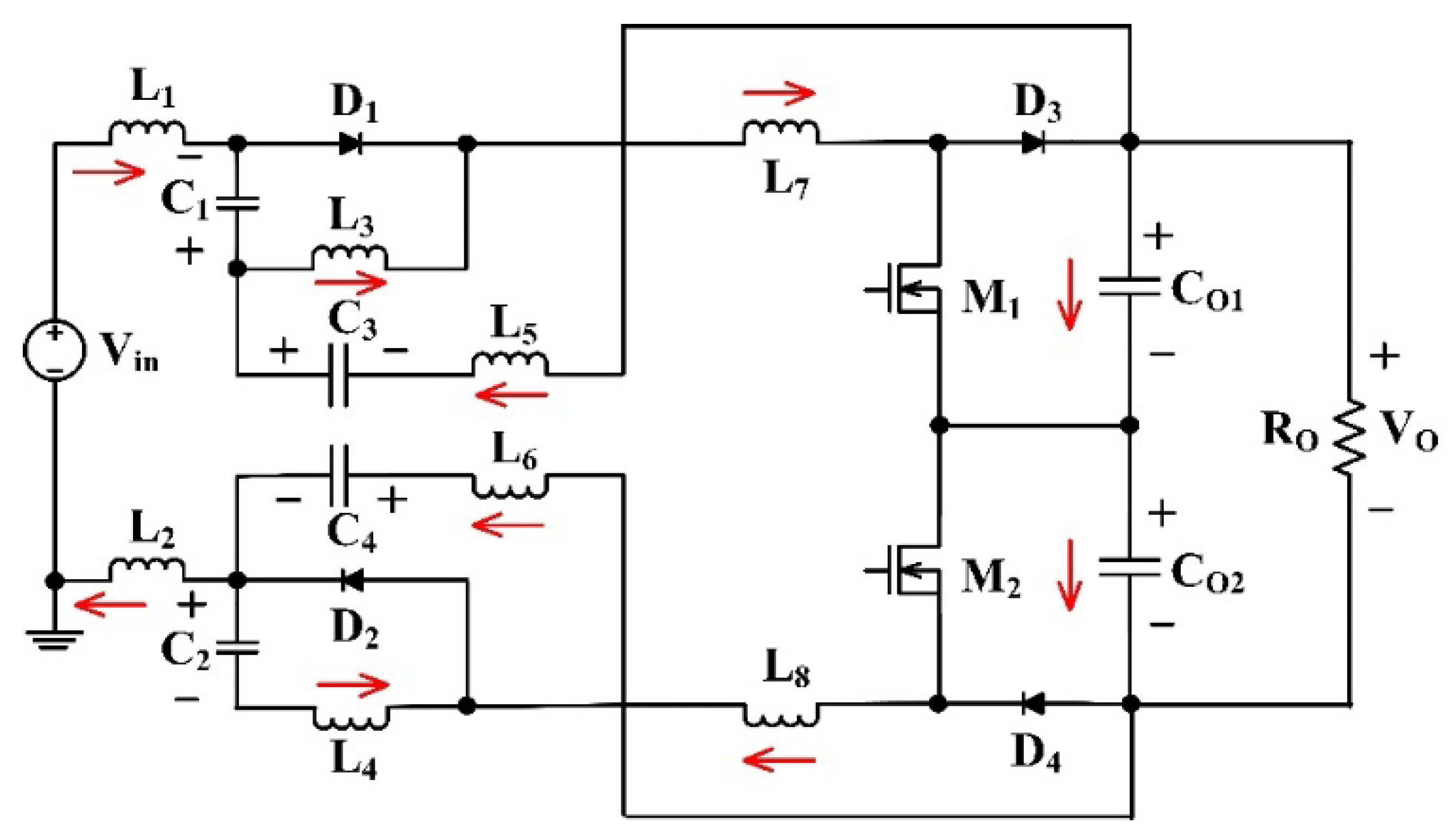
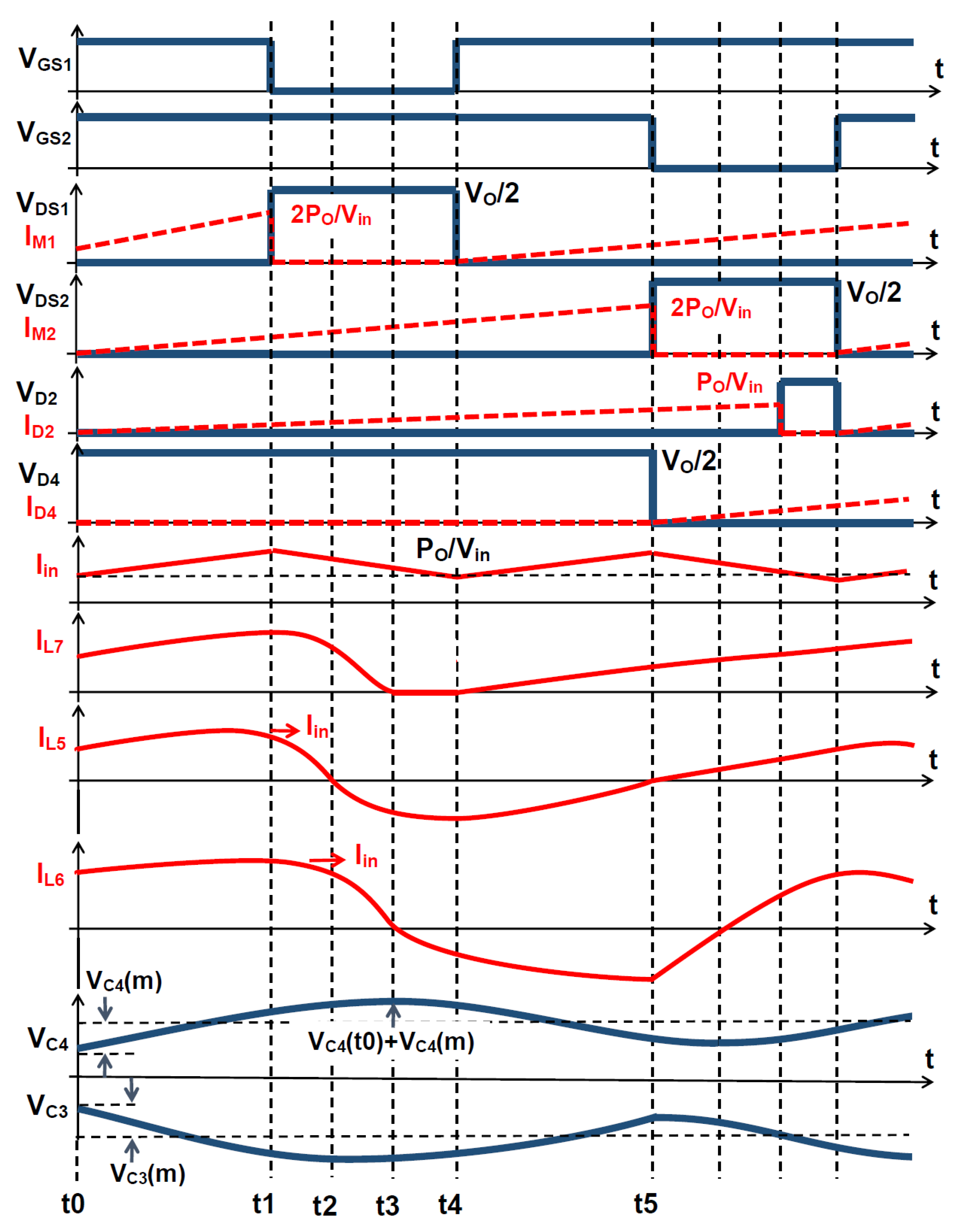
The proposed converter is shown in Figure 2. Inductors L1 and L2 act as the input filter inductors. There are two voltage step-up cells with linear operation that are located symmetrically. These cells include: inductors L3 and L4, capacitors C1 and C2, and diodes D1 and D2. Furthermore, the converter has two resonant cells which consist of inductors L5, L6 and capacitors C3, C4. The mentioned cells are also positioned symmetrically. Two series inductors L7 and L8 tune the current that flows through the linear and resonant cells. Output diodes D3 and D4 are used to transfer the power to the load. Capacitors CO1 and CO2 are usually used in conventional TLDCs. It should be noted that the voltage across each capacitor is equal to half of the output voltage. The theoretical waveforms are shown in Figure 3.

3. Consideration of Operating Modes

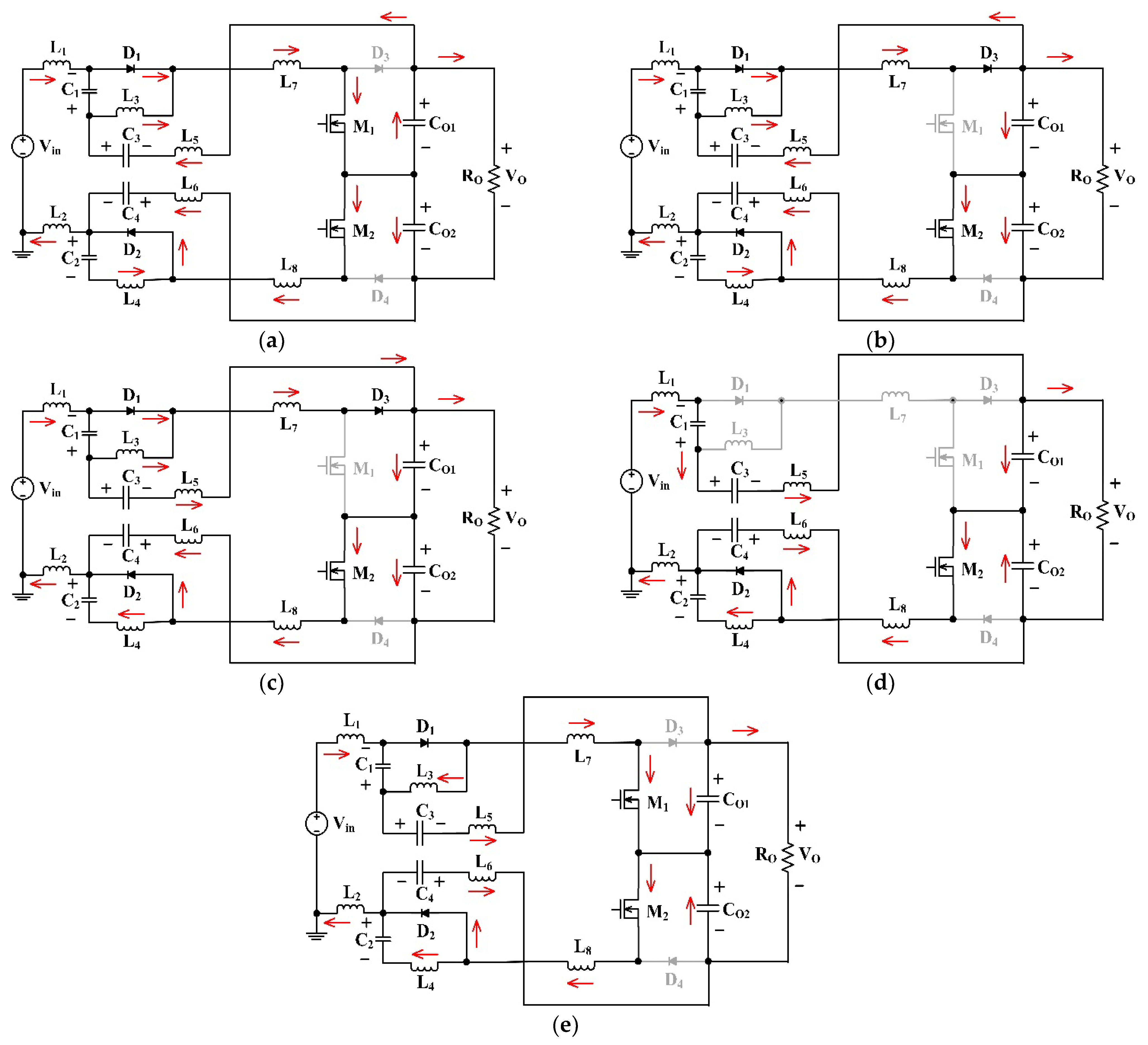
Interval 1: (t0t1) [seeFigure 4a]: This mode starts when switch M2 is turned on at t0, while switch M1 is also turned on. Since switch M2 is connected in series with inductor L8, which has zero current at t0, the switch is turned on under ZCS condition. Hence, diode D4 is also switched off at zero current. On the other hand, diode D2 is switched on under ZCS condition to flow inductor current IL8.
I D 2 = I L 4 + I L 8 = I L 2 + I L 4 I L 6
During this mode, capacitors C1 and C2 are charging. Moreover, capacitor C3 charges while capacitor C4 discharges.
I L 6 = I C O 2 + I O
I C O 1 = I O + I L 5
I L 7 = I M 1 = I M 2 + I C O 1 + I C O 2
V i n 2 = V L 1 + V L 7
Since the proposed converter has a symmetric structure, VL1 = −VL2, VC1 = VC2, and L3 = L4.
t 1 t 0 = V C 1 L 3 Δ I L 3 = V C 2 L 4 Δ I L 4
During this mode, a resonance starts between capacitor C3 and inductor L5. In this condition, the capacitor voltage decreases, and the inductor current increases in a resonance manner.
V C 3 ( t ) = V C 3 ( t 0 ) + V C 3 ( m ) sin ω r 1 ( t t 0 )
i L 5 ( t ) = i L 5 ( t 0 ) cos ω r 1 ( t t 0 )
Furthermore, another resonance occurs between capacitor C4 and inductor L6. The resonance increases VC4 and decreases IL6.
V C 4 ( t ) = V C 4 ( t 0 ) + V C 4 ( m ) sin ω r 2 ( t t 0 )
i L 6 ( t ) = i L 6 ( t 0 ) cos ω r 2 ( t t 0 )
ω r 1 = ω r 2 = 1 C 3 L 5 = 1 C 4 L 6
During this mode, diode D1 is switched on to transfer the energy stored in the input filter inductors to series inductors (L7 and L8). At the end of this mode, inductor current IL5 reaches Iin.
t 1 t 0 = arccos ( I i n i L 5 ( t 0 ) ) ω r 1
V C 3 ( t 1 ) = V C 3 ( t 0 ) + V C 3 ( m ) 1 ( I i n i L 5 ( t 0 ) ) 2
V C 4 ( t 1 ) = V C 4 ( t 0 ) + V C 4 ( m ) 1 ( I i n i L 5 ( t 0 ) ) 2
i L 6 ( t 1 ) = i L 6 ( t 0 ) i L 5 ( t 0 ) I i n
Besides, the following equations are obtained for mode 1.
Δ I L 3 = L 3 ω r 1 V C 1 arccos ( I i n i L 5 ( t 0 ) )
Δ I L 4 = L 4 ω r 1 V C 2 arccos ( I i n i L 5 ( t 0 ) )
i C 3 ( t ) = i L 5 ( t ) i L 5 ( t 0 ) = C 3 V C 3 ( m ) ω r 1
i C 4 ( t ) = i L 6 ( t ) i L 6 ( t 0 ) = C 4 V C 4 ( m ) ω r 2
In fact, mode 1 ends when switch M1 is turned off at t1.
Interval 2: (t1t2) [seeFigure 4b]: This mode starts when switch M1 is turned off at t1 while switch M2 is still turned on. When switch M1 is turned off, diode D3 is switched on and conducts the current that flows through inductor L7. During this mode, diodes D1 and D2 are switched on as same as the former mode. A resonance starts between C3, L5, L7, and C1 in this mode. Hence, inductor current IL5 and capacitor voltage VC3 decrease in a resonance manner. At the end of this mode, the inductor current reaches zero, and the capacitor voltage will be equal to −Vo/2.
i L 5 ( t ) = I i n cos ω r 3 ( t t 1 )
V C 3 ( t ) = V C 3 ( t 1 ) V C 3 ( m ) sin ω r 3 ( t t 1 )
t = t 2 i L 5 ( t 2 ) = 0 t 2 t 1 = 1 4 f 3
t = t 2 V C 3 ( t 1 ) V C 3 ( m ) = V O 2
V C 3 ( t 0 ) = V C 3 ( m ) ( 1 1 ( I i n i L 5 ( t 0 ) ) 2 ) V O 2
The resonance between C4 and L6 continues as same as mode 1.
ω r 3 = 1 C e q 1 L e q 1
C e q 1 = C 1 C 3 C 1 + C 3
L e q 1 = L 5 + L 7
Interval 3: (t2t3) [seeFigure 4c]: This mode starts when inductor current IL5 reaches zero at t2. As a result, the inductor current will be reversed during this mode. The current that flows through inductor L7 decreases and reaches zero at the end of this mode. In addition, diodes D1 and D3 are switched off under ZCS condition at t3. During this mode, the resonance continues between C4 and L6. Finally, inductor current IL6 reaches zero, and the voltage across capacitor C4 reaches its peak value.
t = t 3 i L 6 ( t 3 ) = 0 t 3 t 0 = 1 4 f 2
t = t 3 V C 4 ( t 3 ) = V C 4 ( t 0 ) + V C 4 ( m )
t 3 t 2 = ( t 3 t 0 ) ( t 1 t 0 ) ( t 2 t 1 ) = 1 4 ( 1 f 2 1 f 3 ) arccos ( I i n i L 5 ( t 0 ) ) ω r 2
Δ I L 4 = V C 2 L 4 ( t 3 t 2 )
Δ I L 3 = V C 1 L 3 ( t 3 t 2 )
During this mode, inductor current IL8 increases.
Interval 4: (t3t4) [seeFigure 4d]: This mode starts when IL7 reaches zero and diodes D1 and D3 are switched off under ZCS condition. Besides, IL3 also equals zero at t3. Consequently, the energies stored in the input source, input filter inductors, capacitor C1, and inductor L5 are transferred to the output and capacitor C3. During this mode, the resonance between capacitor C3 and inductor L5 stops. On the other hand, inductor current IL6 will be reversed. As a result, a new resonance occurs among inductors L6, L8, and capacitor C4 through diode D2 and switch M2. Hence, IL6 increases based on the direction, which is shown in Figure 4d.
i L 6 ( t ) = i L 6 ( m ) sin ω r 4 ( t t 3 )
V C 4 ( t ) = V C 4 ( t 0 ) + V C 4 ( m ) cos ω r 4 ( t t 3 )
ω r 4 = 1 C 4 L e q 2
L e q 2 = L 6 + L 8
This mode ends when switch M1 is turned on at t4.
Interval 5: (t4t5) [seeFigure 4e]: This mode starts when switch M1 is turned on at t4 while switch M2 is still turned on. As same as the former mode, diodes D3 and D4 are reverse biased. When switch M1 is turned on, the current that flows through inductor L7 increases from zero. Thus, the switch is turned on under ZCS condition at t4.
t 5 t 4 = L e q 3 V i n Δ I L e q 3
L e q 3 = L 7 + L 8
During this mode, a resonance starts between capacitor C3 and inductor L5. In this condition, the inductor current is reduced, and the capacitor voltage rises.
V C 3 ( t ) = V C 3 ( t 4 ) + V C 3 ( m ) sin ω r 1 ( t t 4 )
i L 5 ( t ) = i L 5 ( t 4 ) + V C 3 ( m ) ω r 1 cos ω r 1 ( t t 4 )
Similar to mode 4, the resonance between inductors L6, L8, and capacitor C6 through diode D2 and switch M2 continues. On the other hand, the energy stored in inductor L3 is transferred to capacitor C1, while the energy stored in capacitor C2 is transmitted to inductor L4. This mode terminates when switch M2 is turned off at t5.

4. Small Signal Modelling

Small signal modeling is used to analyze the stability of a closed-loop system. This method is used by a state space average model. In this model, state space variables are capacitor voltage and inductor current. By considering the converter operating in CCM, state space equations can be calculated as follows.
x ^ ( t ) = A j x ( t ) + B u ( t )
y ( t ) = C j x ( t ) + D u ( t )
where, x(t) is the state space variable, x ^ ( t ) is derivative of x(t), and A, B, C and D, respectively, denote the matrices of the state, input, output and input–output. Besides, j is the number of operation modes in the proposed converter (j = 1, 2,…,5). Due to symmetric structure of the proposed converter, state variables are defined as follows.
x ( t ) = [ i L 1 i L 3 i L 5 i L 7 V C 1 V C 3 V C O 1 ]
u ( t ) = [ V i n i i n ] & y = [ V O ]
Kirchhoff’s laws in Mode 1 leads to the following equations.
d i L 1 d t = V i n + V C 1 2 V C 3 V O 2 L 1
d i L 3 d t = V C 1 L 3
d i L 5 d t = V O 2 L 5 V C O 2 L 5
d i L 7 d t = V O + 2 V C 3 V C 1 2 L 7
d V C 1 d t = i L 5 i L 3 C 1
d V C 3 d t = i L 5 C 3
d V C O 1 d t = V O C O 1 R O i L 5 C O 1
Accordingly, Mode 2 yields the following equations.
d i L 1 d t = V i n + V C 1 2 V C 3 V O 2 L 1
d i L 3 d t = V C 1 L 3
d i L 5 d t = V O 2 L 5 V C O 2 L 5
d i L 7 d t = 2 V C 3 + V O V C 1 V C O 1 2 L 7
d V C 1 d t = i L 5 i L 3 C 1
d V C 3 d t = i L 5 C 3
d V C O 1 d t = i L 7 i L 5 V O R O C O 1
The following equations are associated with Mode 3.
d i L 1 d t = V i n + V C 1 2 V C 3 V O 2 L 1
d i L 3 d t = V C 1 L 3
d i L 5 d t = V C O 1 V O V C 1 2 L 5
d i L 7 d t = 2 V C 3 + V O V C 1 V C O 1 2 L 7
d V C 1 d t = i L 5 i L 3 C 1
d V C 3 d t = + i L 5 C 3
d V C O 1 d t = i L 7 + i L 5 V O R O C O 1
Applying Kirchhoff’s laws to Mode 4 yields:
d i L 1 d t = V i n V O + V C 1 2 V C 3 2 L 1
d i L 3 d t = 0
d i L 5 d t = V i n V O 2 V C 3 L 5
d i L 7 d t = 0
d V C 1 d t = i L 1 C 1
d V C 3 d t = i L 1 C 3
d V C O 1 d t = i L 5 V O R O C O 1
Eventually, by inspection, the associated equations with Mode 5 are as follows.
d i L 1 d t = V i n + V C 1 2 V C 3 V O 2 L 1
d i L 3 d t = V C 1 L 3
d i L 5 d t = V O 2 L 5 V C O 2 L 5
d i L 7 d t = V O + 2 V C 3 V C 1 2 L 7
d V C 1 d t = i L 3 C 1
d V C 3 d t = i L 5 C 3
d V C O 1 d t = i L 5 V O R O C O 1
Aave, Bave, and Cave can be determined by state space averaging as follows.
A a v e = [ 0 0 0 0 1 2 L 1 1 L 1 0 0 0 0 0 1 L 3 0 0 0 0 0 0 D 3 2 L 5 2 D 4 L 5 D 3 2 ( D 1 + D 2 + D 5 ) 2 L 5 0 0 0 0 ( D 1 + D 2 + D 3 + D 5 ) 2 L 7 D 1 + D 2 + D 3 + D 5 L 7 ( D 2 + D 3 ) 2 L 7 D 4 C 1 D 5 ( D 1 + D 2 + D 3 ) C 1 D 1 + D 2 D 3 C 1 0 0 0 0 D 4 C 3 0 D 3 ( D 1 + D 2 + D 5 ) C 3 0 0 0 0 0 0 1 C O 1 D 2 + D 3 C O 1 0 0 0 ]
B a v e = [ 1 2 L 1 0 0 0 D 4 L 5 0 0 0 0 0 0 0 0 0 ]
C a v e = [ 1 2 L 1 0 D 1 + D 2 + D 5 D 3 2 D 4 2 L 5 D 1 + D 2 + D 3 + D 5 2 L 7 0 0 1 R C O 1 ]
The Laplace transform can be applied to the matrices above to derive the open-loop signal-to-output transfer functions.
G ( S ) = Y ( S ) U ( S ) = C a v e [ S I A a v e ] 1 + D
Open loop conversion function is obtained by substituting (80) and (82) into (83). Zeros and poles of the conversion function at the continuous time state space can be reached by using Gzpk command in MATLAB software. Obtained zeros and poles lie within the left-half of the s-plane. As a result, the open loop conversion function is stable.

5. Design Considerations

This part explains the design consideration of the proposed converter. The essential equations to design different parts are presented. Furthermore, the selection of elements based on the design guidelines and obtained values are described in detail. It should be noted that the proposed converter has a symmetric structure. In this condition, the elements in the symmetric parts have the same values.

5.1. Design of Input Filter Inductors L1, L2

The calculation of the input filter inductors in the proposed converter is similar to a conventional boost converter. Since L1 and L2 have equal inductances and they are connected in series with each other, the following equation is obtained.
L 1 = L 2 V i n D k 4 Δ I L 1 f s w
In (84), Dk indicates the on-time duration of both switches M1 and M2. ΔIL1 represents the half value of the current ripple that flows through input inductors. It should be designed in such a way that the proposed converter operates in CCM.

5.2. Design of Output Capacitors Co1, Co2

Since the proposed topology is a three-level converter that has a symmetric structure, CO1 and CO2 are equal. These capacitors act as an output filter.
C O = C O 1 × C O 2 C O 1 + C O 2
The output capacitor in the worst condition in CCM operation can be calculated as follows.
C O = D k 2 R ( Δ V O V O ) f s w
C O = C O 1 2
C O 1 = C O 2 = D k 4 R ( Δ V O V O ) f s w
In (86) and (88), R indicates the output load resistor and ΔVO/VO calculates the relative error in the output voltage.

5.3. Design of Series Inductors L7, L8

According to the converter operation in mode 5, the following equations are reached.
L 7 = L 8 = L e q 3 2 = L 7 + L 8 2
L 7 = L 8 = 2 V i n D 5 T s w 2 Δ I L 7
Inductors L7 and L8 can be operated either in resonant or linear modes in the proposed converter. The maximum current that flows through the inductors is equal to the peak resonant current.
Δ I L 7 = Δ I L 8 = i L 5 ( m ) = i L 6 ( m ) = I i n

5.4. Design of Inductors L3, L4

Inductors L3 and L4 have equal inductances.
L 3 = L 4 = V C 1 2 Δ I L 3 ( D 1 + D 2 ) T s w
( D 1 + D 2 ) T s w 2 = t 2 t 0
In (92), ΔIL3 = ΔIL4. Moreover, their values are equal to half the peak-to-peak current that flows through L3 and L4.

5.5. Design of Capacitors C1, C2

Based on the capacitor charge balance, the following equations are computed.
1 T s w 0 T s w i C 1 ( t ) d t = i C 1 ( t ) = 0
0 ( D 1 + D 2 ) T s w 2 i C 1 ( t ) d t = ( D 1 + D 2 ) T s w 2 ( D 3 + D 4 + D 5 ) T s w 2 i C 1 ( t ) d t
D 1 + D 2 = 1 2 ( D 3 + D 4 + D 5 )
Since the capacitors have linear operation, the following equation can be used.
C 1 Δ V C 1 = i C 1 ( t ) ( D 1 + D 2 ) T s w 2
Based on the converter operation during modes 1 and 2, the following formula is obtained.
i C 1 ( t ) = I i n + i L 7 ( t ) + i L 3 ( t )
Because iL3 has a small value, it is ignored.
i C 1 ( t ) = I i n + i L 7 ( m ) = 2 P O V i n
C 1 = C 2 = 2 I i n Δ V C 1 ( D 1 + D 2 ) T s w
In (100), ΔVC1 is usually 10% of the rated output voltage.

5.6. Design of Switches M1 and M2

Voltage and current stresses should be calculated to select the appropriate type of switches. 50 kHz is selected as the switching frequency for the proposed converter.
V M 1 ( max ) = V M 2 ( max ) = V O ( max ) 2
I M 1 ( max ) = I M 2 ( max ) = I i n + i L 5 ( max ) = 2 P O V i n

5.7. Design of Output Diodes D3, D4

The voltage and current stresses of the diodes can be calculated as follows.
V D 3 ( max ) = V D 4 ( max ) = V O ( max ) 2
I D 3 ( max ) = I D 4 ( max ) = I O + P O V i n

5.8. Design of Input Diodes D1, D2

Voltage and current stresses of the diodes can be considered as follows.
V D 1 ( max ) = V D 2 ( max ) = V C 1 ( max ) = V C 2 ( max )
I D 1 ( max ) = I D 2 ( max ) = P O V i n

5.9. Design of Resonant Elements C3, C4, L5, L6

The maximum current that flows through the resonant elements is considered equal to the input current.
I i n = P O V i n I L 5 = I L 6 = V C 3 ( m ) Z r 1
Z r 1 = L 5 C 3
By considering 20% as over-design, the following equation is computed.
Z r 1 = V C 3 ( m ) 0.6 I i n
According to the converter operation, the resonant frequency should be at least twice the switching frequency.
T r e s = 2 π C 3 L 5 T s w 2
By using (109) and (110), the values of resonant inductors (L5 = L6) and resonant capacitors (C3 = C4) are obtained. It should be noted that the voltage gain of the proposed converter in CCM can be calculated as follows.
G C C M = 2 1 2 D

6. Control of the Proposed DC-DC Converter

Figure 5 shows the general block diagram of the control circuit followed by the detailed diagram presented in Figure 6. The first two blocks, i.e., the output sampler and isolator, are realised through TL431. These are then followed by error amplifier and a PID compensator block. This is eventually directed to the SG3527 for PWM and then to the pulse delay circuit to adjust the produced signal.
At different loads, the output voltage should be stabilized by the control circuit. Hence, the influence of load variations on the output voltage is illustrated in Figure 7. As can be shown from the figure, the control circuit performs well during sudden load changes. Changing of the load is 25 to 100% and 50 to 100% of the rated load in Figure 7a,b, respectively.

7. Simulation and Experimental Results

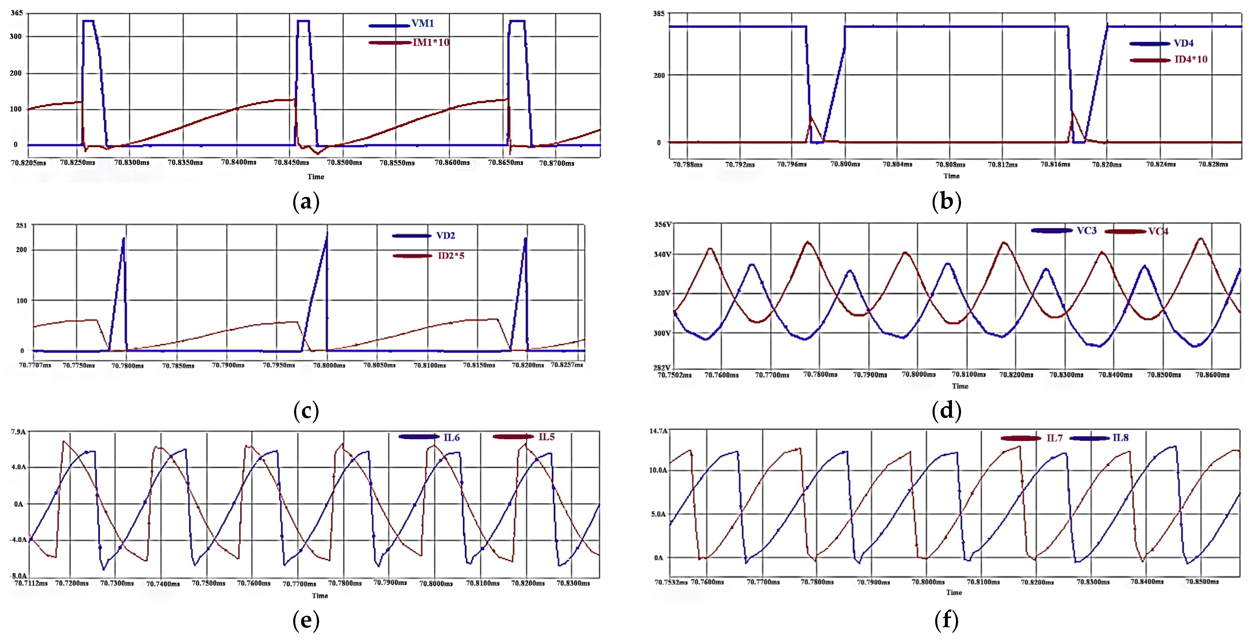
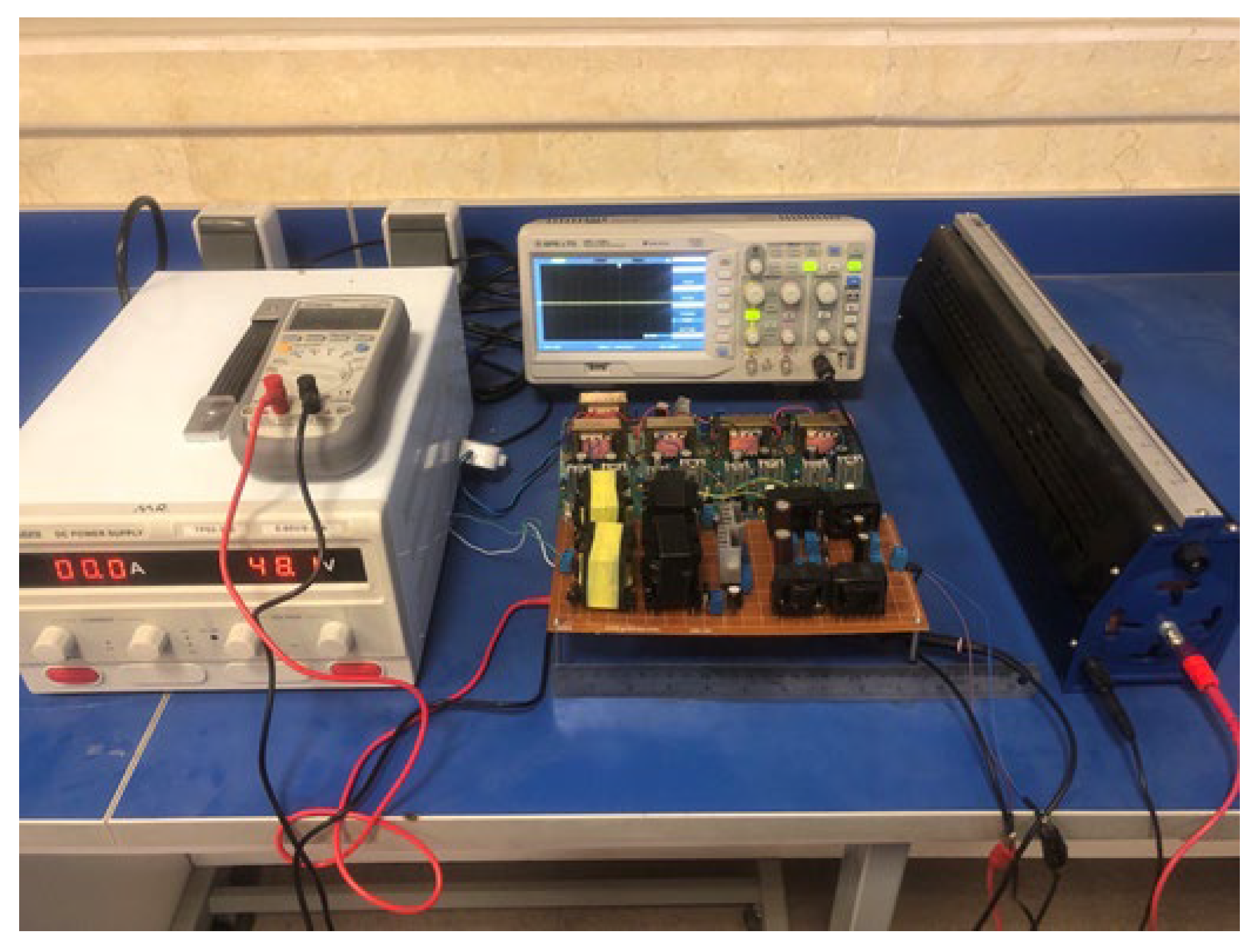
To confirm the theoretical analysis of the proposed converter, simulation waveforms using Pspice software are shown in Figure 8. Moreover, a prototype of the proposed converter is constructed. According to the design consideration, the value for each element is presented in Table 1. A prototype of the proposed converter is presented in Figure 9.
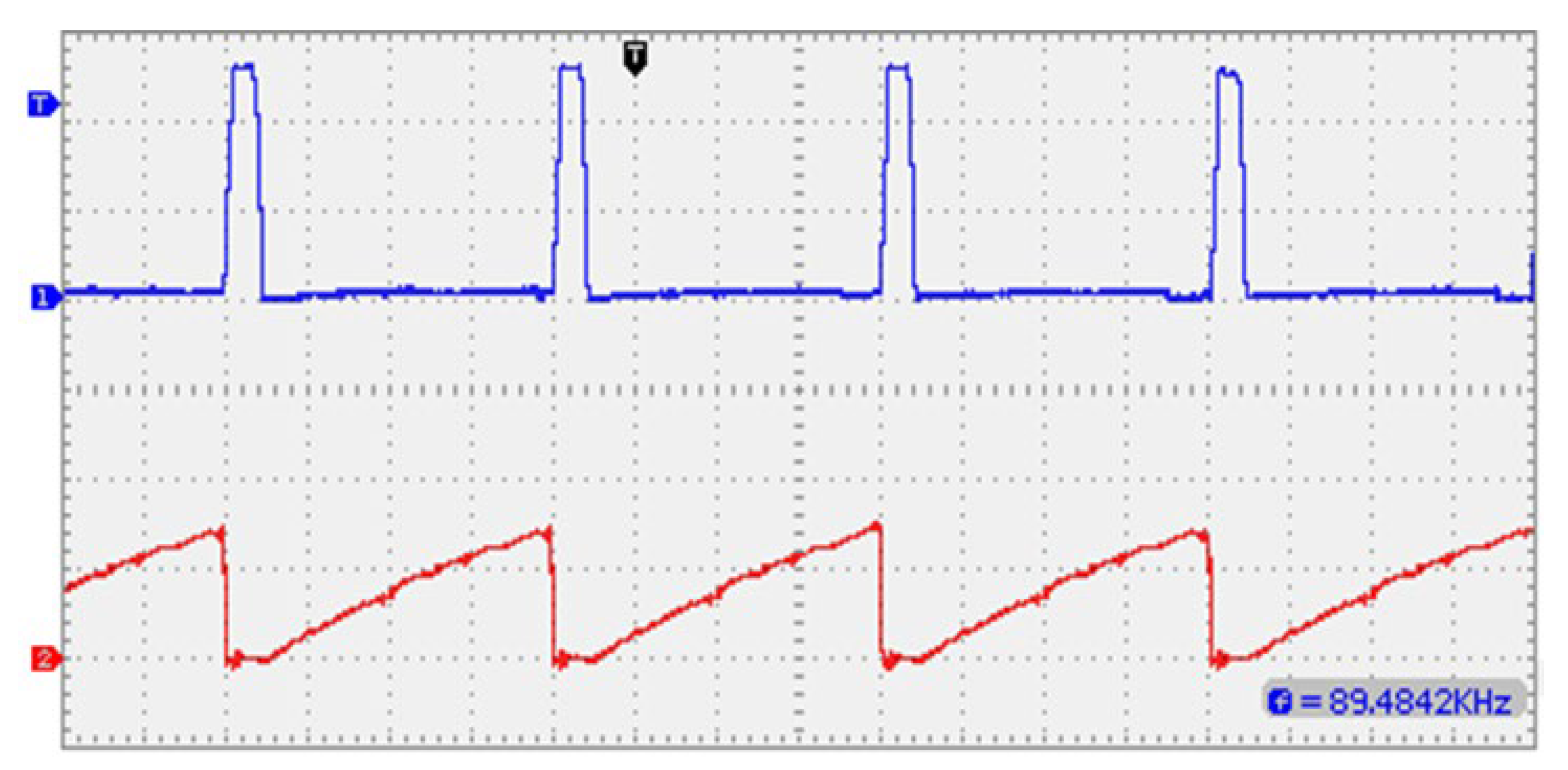
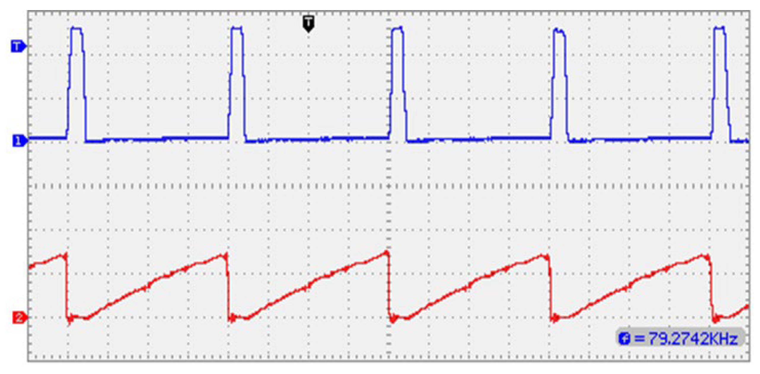
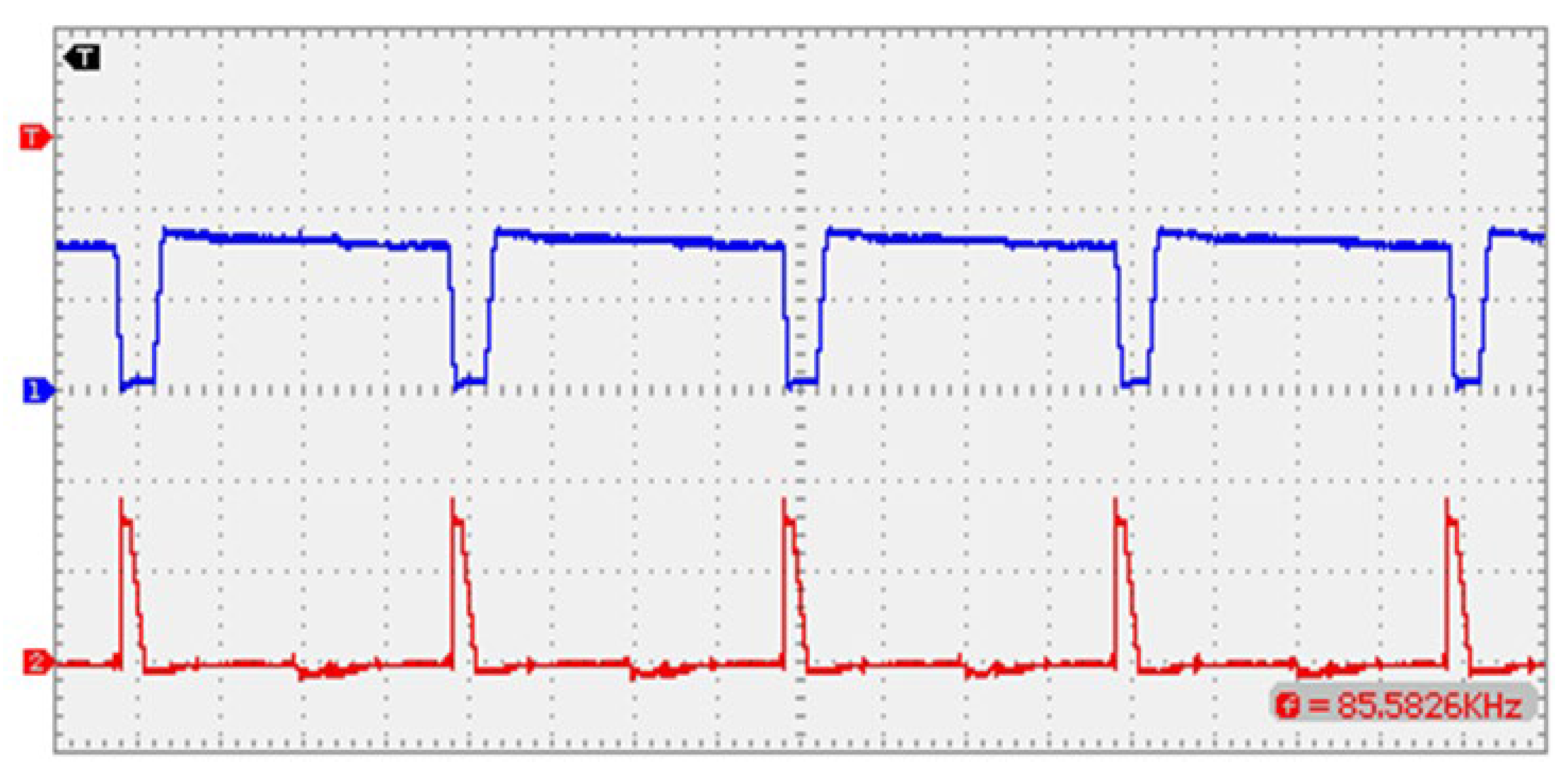
The derived voltage and current waveforms of the active power switches M2 and M1 are, respectively, shown in Figure 10 and Figure 11. According to the converter operation in mode 1, the switch is turned on under ZCS condition. This is performed because the switch is connected in series with inductor L8, which has zero current at t0. Due to the symmetric structure, the waveforms of switch M1 are similar to M2. The gating signals of the TLDC should have a phase difference of 180 degrees to each other.
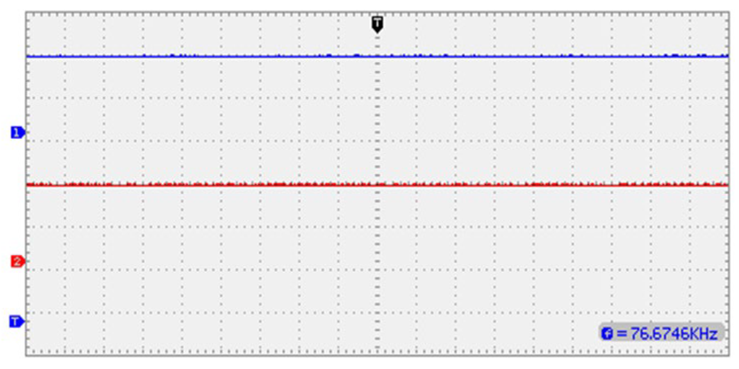
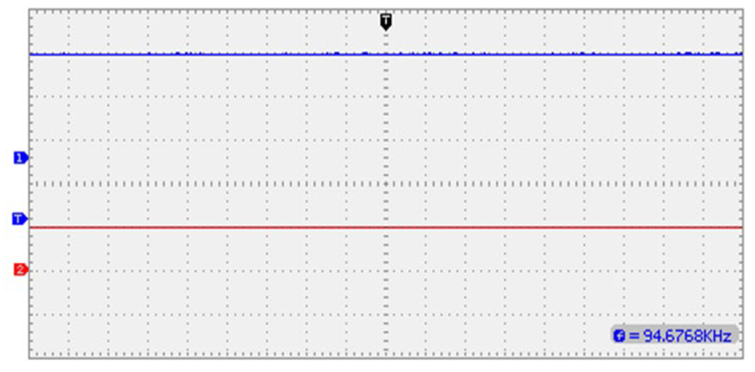
The output capacitors, i.e., CO1 and CO2, operate as expected with the dc voltage waveforms shown in Figure 12. Due to the three-level structure, the voltage across each capacitor is equal to half of the output voltage. Figure 13 illustrates the input and output voltages.
Figure 14 presents the voltage and current waveforms of diode D4, which is connected in series with inductor L8. Based on the converter operation in mode 1, the diode is switched off under ZCS condition when switch M2 is turned on. Due to the symmetric structure, the voltage and current waveforms of diode D3 are similar to diode D4.
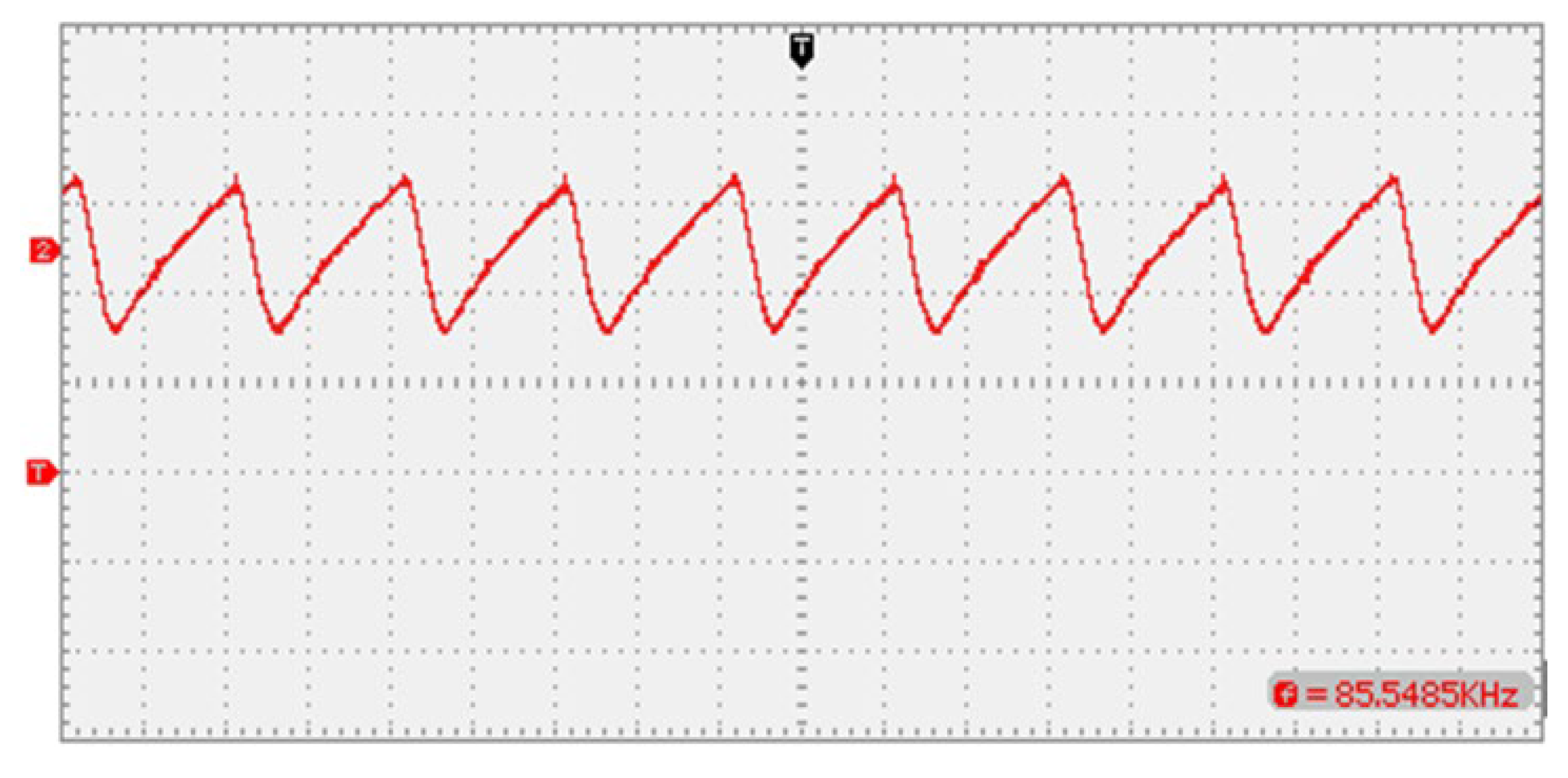
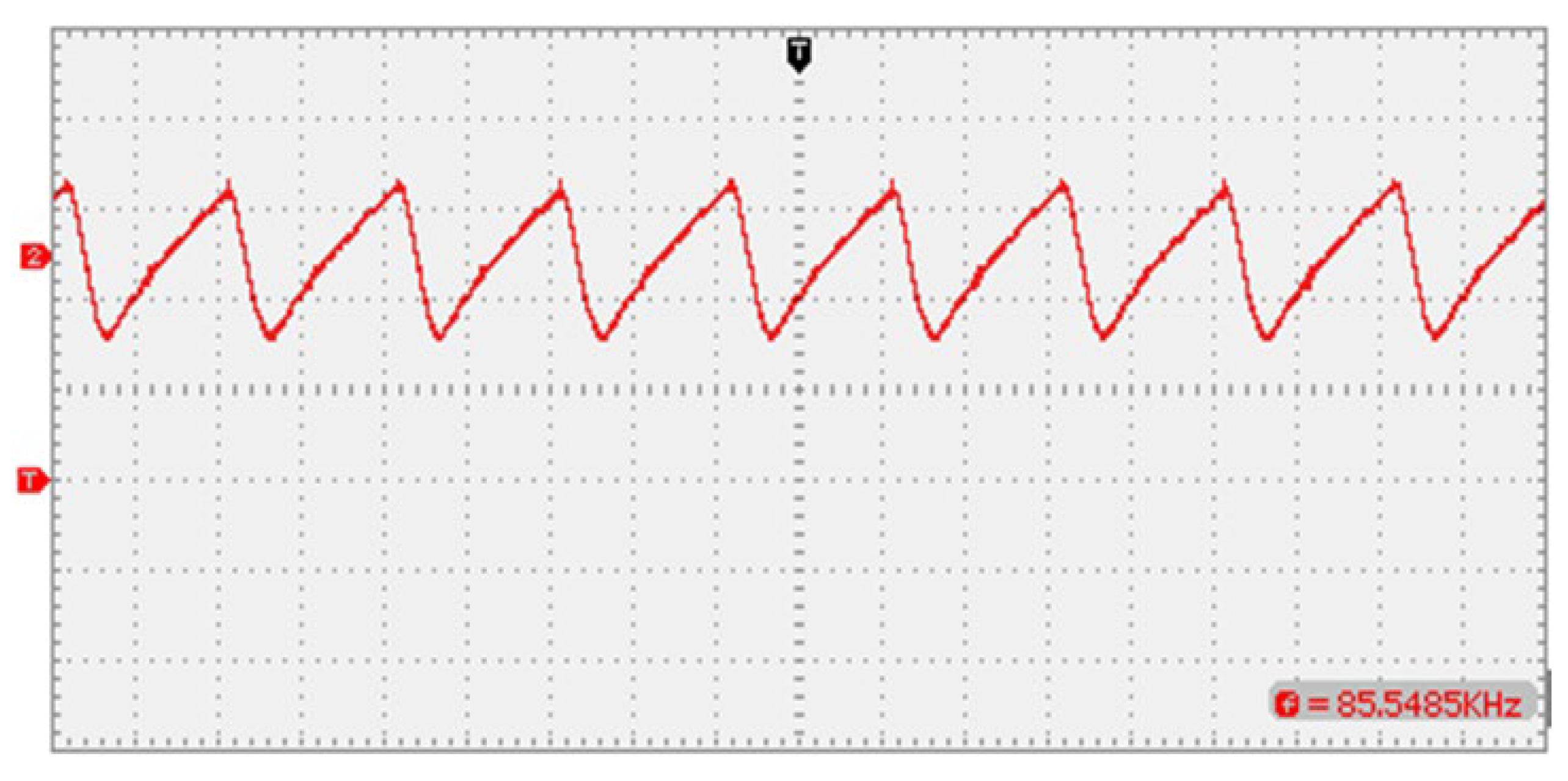
Inductor currents IL7 and IL8 are shown in Figure 15. Moreover, inductor current IL3 is depicted in Figure 16. As mentioned earlier, IL3 increases and decreases linearly.
In the second half of the switching cycle, inductor current IL4 is similar to IL3. Capacitor voltage VC1 is presented in Figure 17. Due to the symmetric structure, capacitor voltage VC2 is similar to VC1 in the second half of the switching cycle.
Voltage and current waveforms of diode D2 are displayed in Figure 18. The diode is forward-bioased under ZCS at t0 to flow IL8.
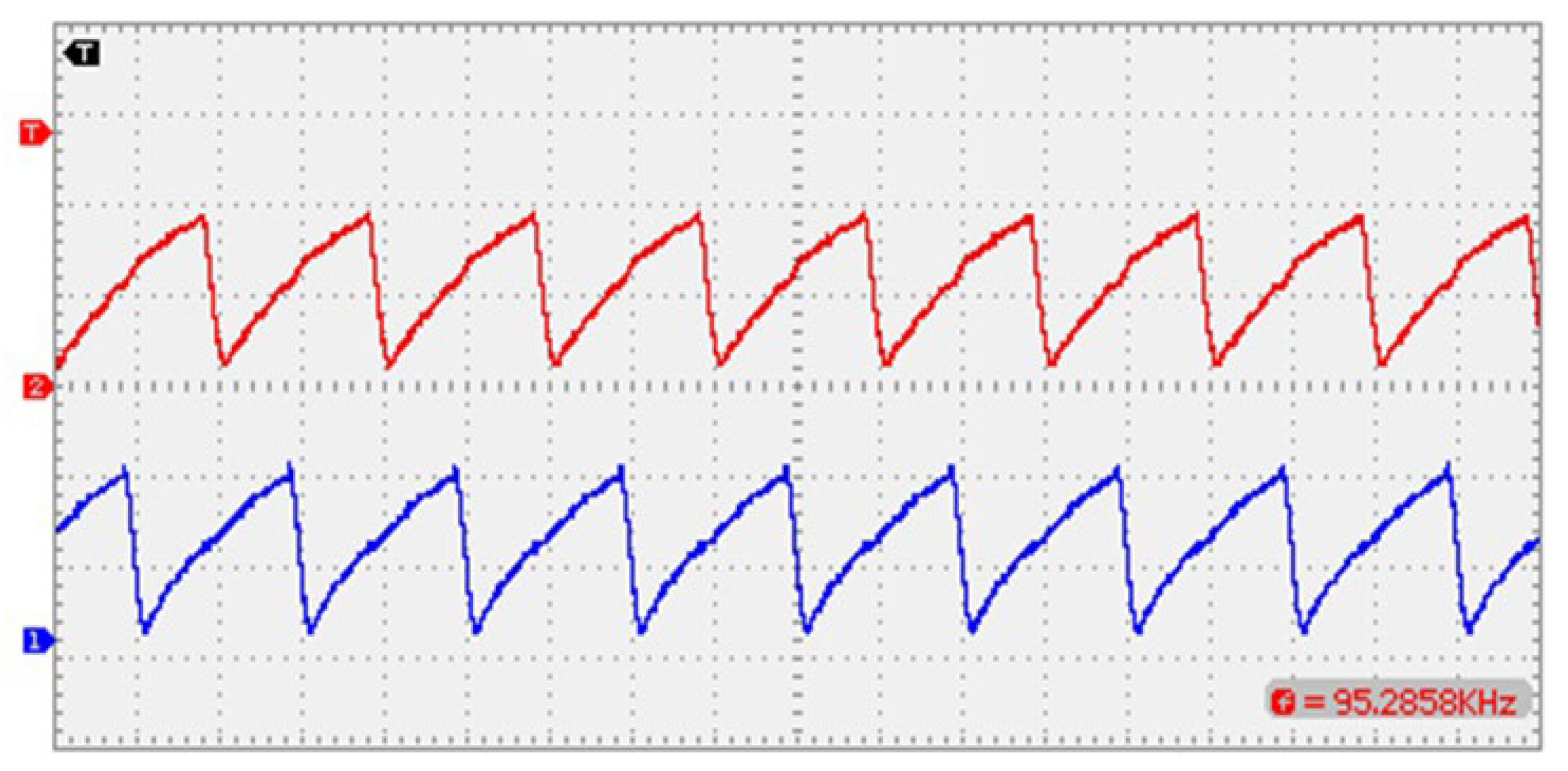
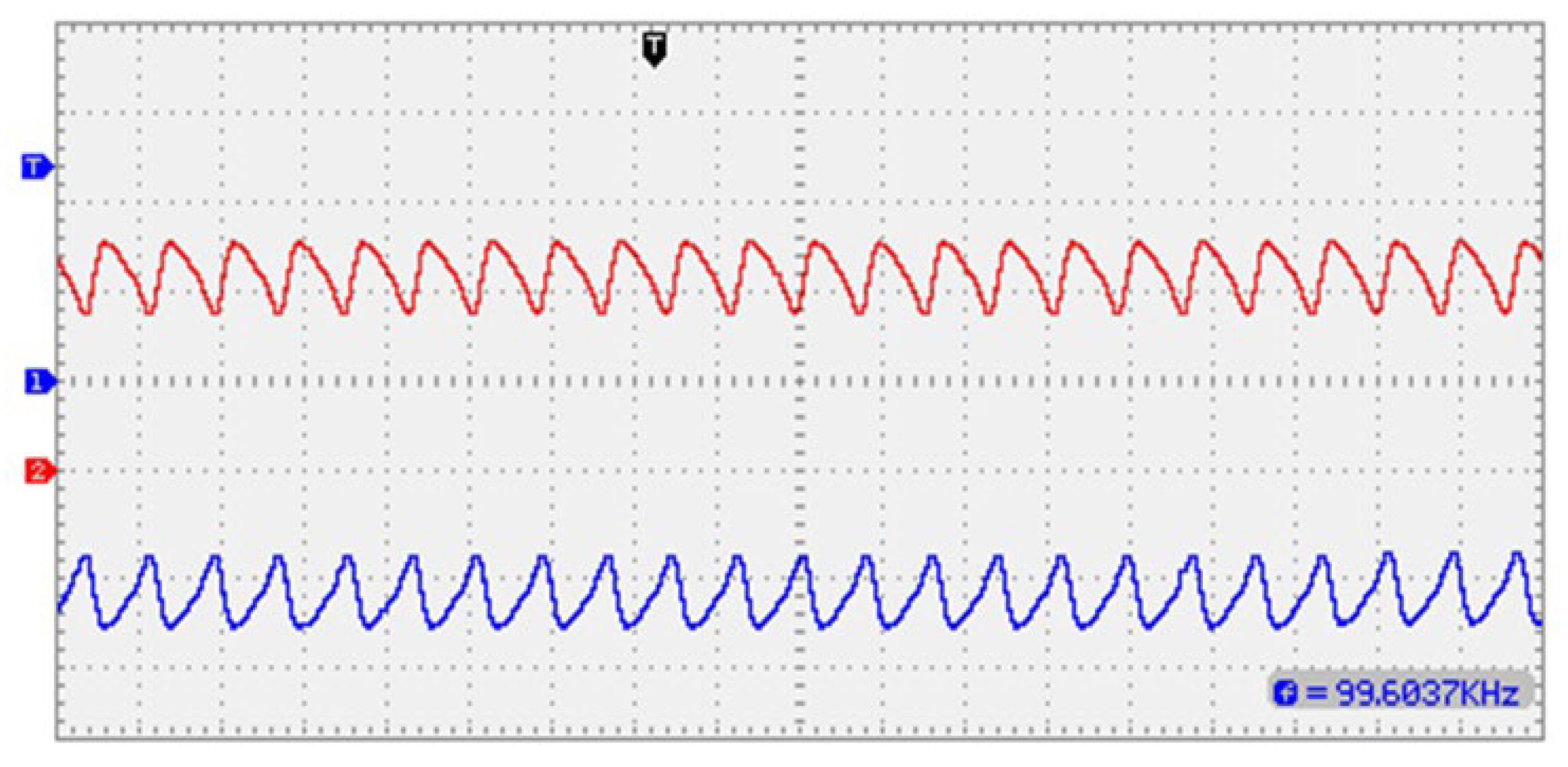
Voltage waveforms of resonant capacitors C3 and C4 are shown in Figure 19. In addition, current waveforms of resonant inductors L5 and L6 are depicted in Figure 20.
The comparison between the proposed converter and other high step-up TLDCs in terms of voltage gain, voltage stress, soft switching, switching frequency, and the number of active elements is presented in Table 2.
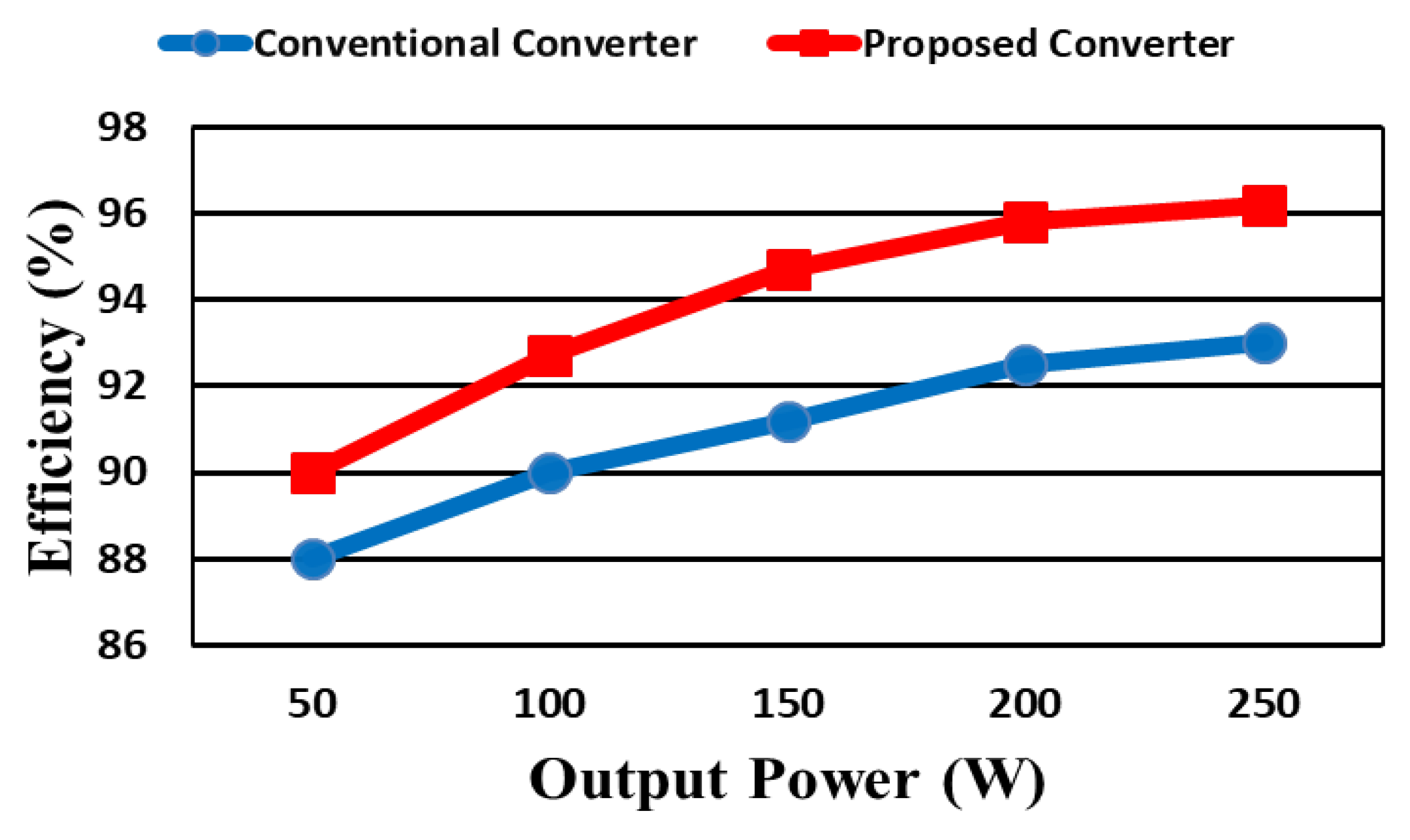
Figure 21 show the efficiency variations with variations in the output load. Moreover, the operation of the converter under hard switching conditions is also plotted in this figure. It is obvious that the total efficiency of the proposed converter under soft-switching conditions is equal to 96.2% at full load.
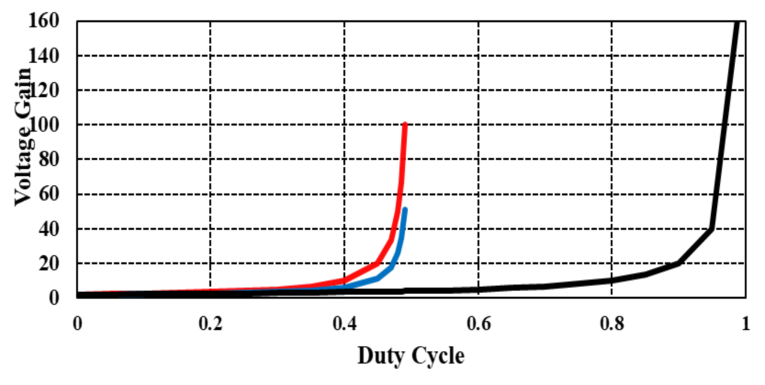
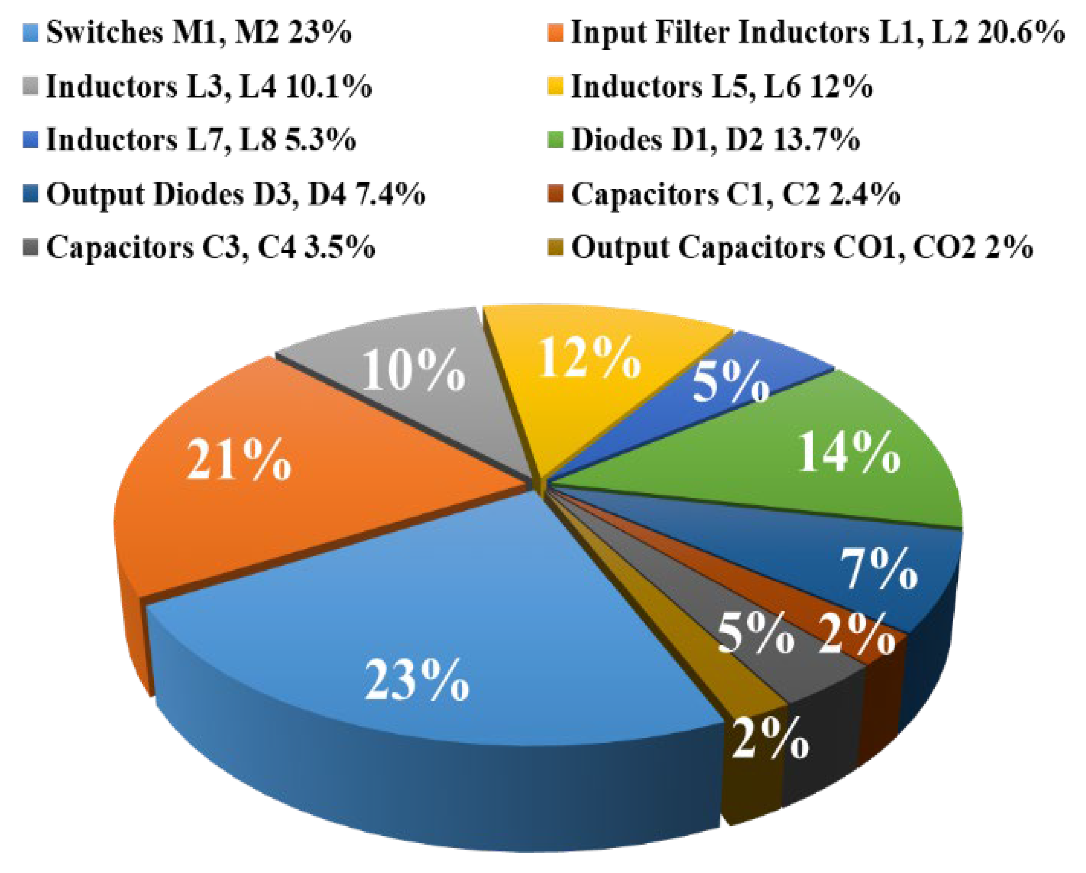
The voltage gain obtained by (111) is shown in Figure 22 for different values of the duty cycle. It is obvious that the voltage gain of the proposed converter is sufficiently high that it can be used for PV applications. Moreover, the voltage gains of other selected converters are depicted in Figure 22 to compare with the proposed converter. The power loss distribution at 250 W for the proposed TLDC is plotted in Figure 23. To explain Figure 23, power loss calculation with details is shown in Table 3.

8. Conclusions

A Three-level DC-DC converter has been proposed, which benefits from a high voltage gain and a symmetric structure. The voltage gain ratio can reach up to 15 times, while no transformer or coupled inductor has been used. This high step-up capability is achieved by using two high step-up cells and two resonant paths in the converter topology. The converter has low input current ripple. Moreover, the voltage and current stresses of the switches are quite low. As the zero current switching has been achieved, the switching losses have been lowered, and the total efficiency of the proposed converter reaches 96.2% at full load. The proposed converter uses simple PWM to trigger only two power switches in its structure. A comprehensive comparison with the existing topologies, as well as simulations and experiments on a 250 W prototype, have confirmed the analysis for the operating conditions of 48 V as the input voltage and 700 V as the output voltage, with a switching frequency of 50 kHz

Author Contributions

Conceptualization, S.S.T., M.R. and A.M.; methodology, S.S.T., M.R. and A.M.; software, S.S.T., M.R. and A.M. validation, S.S.T., M.R. and A.M.; writing—original draft preparation, S.S.T., M.R. and A.M.; writing—review and editing, S.A.G.; visualization, S.S.T., M.R. and A.M.; supervision, S.A.G.; project administration, A.M. All authors have read and agreed to the published version of the manuscript.

Funding

This research received no external funding.

Conflicts of Interest

The authors declare no conflict of interest.

References

  1. Jagadeesh, I.; Indragandhi, V. Comparative Study of DC-DC Converters for Solar PV with Microgrid Applications. Energies 2022, 15, 7569. [Google Scholar] [CrossRef]
  2. Asghari-Gorji, S.; Ektesabi, M. Input current ripples cancellation in bidirectional switched-inductor quasi-Z-source inverter using coupled inductors. In Proceedings of the 2015 Australasian Universities Power Engineering Conference (AUPEC), Wollongong, NSW, Australia, 27–30 September 2015; pp. 1–6. [Google Scholar]
  3. Mirzaei, A.; Rezvanyvardom, M. High voltage gain soft switching full bridge interleaved Flyback DC-DC converter for PV applications. Sol. Energy 2020, 196, 217–227. [Google Scholar] [CrossRef]
  4. Ramirez-Carrillo, M.; Ortega-Cisneros, S.; Rosas-Caro, J.C.; Rivera, J.; Valdez-Resendiz, J.E.; Mayo-Maldonado, J.C.; Valderrabano-Gonzalez, A. A Step-Up Converter with Large Voltage Gain and Low Voltage Rating on Capacitors. Energies 2022, 15, 7944. [Google Scholar] [CrossRef]
  5. He, X.; Hu, R.; Chen, W. A Hybrid Three-Level ZVZCS Converter for Photovoltaic Power Connecting to MVDC Collection System. Energies 2022, 15, 5365. [Google Scholar] [CrossRef]
  6. Tsang, K.M.; Chan, W.L. A single switch DC/DC converter with galvanic isolation and input current regulation for photovoltaic systems. Sol. Energy 2015, 119, 203–211. [Google Scholar] [CrossRef]
  7. Liu, L.; Bala, S.; Canales, F. Stacked DC-DC Converter with Wide Voltage Range. In Proceedings of the 2019 IEEE Energy Conversion Congress and Exposition (ECCE), Baltimore, MD, USA, 29 September–3 October 2019; pp. 1401–1407. [Google Scholar]
  8. Folmer, S.; Stala, R. DC-DC High Voltage Gain Switched Capacitor Converter With Multilevel Output Voltage and Zero-Voltage Switching. IEEE Access 2021, 9, 129692–129705. [Google Scholar] [CrossRef]
  9. Sadaf, S.; Bhaskar, M.S.; Meraj, M.; Iqbal, A.; Al-Emadi, N. A Novel Modified Switched Inductor Boost Converter With Reduced Switch Voltage Stress. IEEE Trans. Ind. Electron. 2021, 68, 1275–1289. [Google Scholar] [CrossRef]
  10. Li, B.; Wang, P.; Wang, Z.; Ma, X.; Bi, H. A New Coupled-Inductor-Based High-Gain Interleaved DC-DC Converter With Sustained Soft Switching. IEEE Trans. Veh. Technol. 2021, 70, 6527–6541. [Google Scholar] [CrossRef]
  11. Matsuda, A.; Koizumi, H.; Sato, T. Two-Stage Interleaved DC-DC Converter with Input-Parallel Output-Series Connection. In Proceedings of the 2019 IEEE International Symposium on Circuits and Systems (ISCAS), Sapporo, Japan, 26–29 May 2019; pp. 1–5. [Google Scholar]
  12. Gorji, S.A. Reconfigurable Quadratic Converters for Electrolyzers Utilized in DC Microgrids. IEEE Access 2022, 10, 109677–109687. [Google Scholar] [CrossRef]
  13. Gorji, S.A.; Sahebi, H.G.; Movahed, M.; Ektesabi, M. Multi-Input Boost DC-DC Converter with Continuous Input-Output Current for Renewable Energy Systems. In Proceedings of the 2019 IEEE 4th International Future Energy Electronics Conference (IFEEC), Singapore, 25–28 November 2019; pp. 1–5. [Google Scholar]
  14. Rodrigues, J.P.; Mussa, S.A.; Barbi, I.; Perin, A.J. Three-level zero-voltage switching pulse-width modulation DC-DC boost converter with active clamping. IET Power Electron. 2010, 3, 345–354. [Google Scholar] [CrossRef]
  15. Yang, L.; Liang, T.; Lee, H.; Chen, J. Novel High Step-Up DC–DC Converter With Coupled-Inductor and Voltage-Doubler Circuits. IEEE Trans. Ind. Electron. 2011, 58, 4196–4206. [Google Scholar] [CrossRef]
  16. Zhang, Y.; Sun, J.T.; Wang, Y.F. Hybrid Boost Three-Level DC–DC Converter With High Voltage Gain for Photovoltaic Generation Systems. IEEE Trans. Power Electron. 2013, 28, 3659–3664. [Google Scholar] [CrossRef]
  17. Macellari, M.; Schirone, L. Design of high-efficiency non-insulated step-up converters. IET Power Electron. 2015, 8, 743–749. [Google Scholar]
  18. Poorali, B.; Jazi, H.M.; Adib, E. Single-core soft-switching high step-up three-level boost converter with active clamp. IET Power Electron. 2016, 9, 2692–2699. [Google Scholar] [CrossRef]
  19. Moradisizkoohi, H.; Elsayad, N.; Mohammed, O.A. Experimental Verification of a Double-Input Soft-Switched DC–DC Converter for Fuel Cell Electric Vehicle With Hybrid Energy Storage System. IEEE Trans. Ind. Appl. 2019, 55, 6451–6465. [Google Scholar] [CrossRef]
  20. Cordeiro, A.; Pires, V.F.; Foito, D.; Pires, A.J.; Martins, J.F. Three-level quadratic boost DC-DC converter associated to a SRM drive for water pumping photovoltaic powered systems. Sol. Energy 2020, 209, 42–56. [Google Scholar] [CrossRef]
  21. Ding, X.; Zhao, D.; Liu, Y.; Li, K.; Hao, Y. High step-up three-level DC–DC converter with three-winding coupled-inductor. J. Power Electron. 2020, 20, 53–64. [Google Scholar] [CrossRef]
  22. Wang, P.; Zhou, L.; Zhang, Y.; Li, J.; Sumner, M. Input-Parallel Output-Series DC-DC Boost Converter With a Wide Input Voltage Range For Fuel Cell Vehicles. IEEE Trans. Veh. Technol. 2017, 66, 7771–7781. [Google Scholar] [CrossRef]
  23. Zhang, Y.; Sumner, L.Z.M.; Wang, P. Single-Switch, Wide Voltage-Gain Range, Boost DC–DC Converter for Fuel Cell Vehicles. IEEE Trans. Veh. Technol. 2018, 67, 134–145. [Google Scholar] [CrossRef]
  24. Zhang, Y.; Shi, J.; Zhou, L.; Li, J. Wide Input-Voltage Range Boost Three-Level DC–DC Converter With Quasi-Z Source for Fuel Cell Vehicles. IEEE Trans. Power Electron. 2017, 32, 6728–6738. [Google Scholar] [CrossRef]
  25. Wu, X.; Yang, M.; Zhou, M.; Zhang, Y.; Fu, J. A Novel High-Gain DC-DC Converter Applied in Fuel Cell Vehicles. IEEE Trans. Veh. Technol. 2020, 69, 12763–12774. [Google Scholar] [CrossRef]
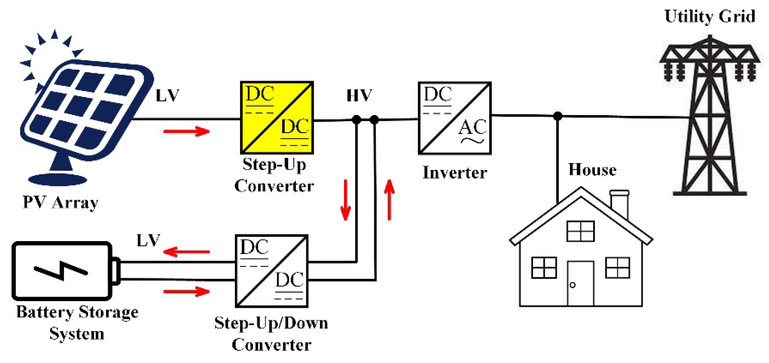
Figure 1. Block diagram of a grid-connected PV system.
Energies 16 00041 g001
Figure 2. The circuit arrangement of the proposed converter.
Energies 16 00041 g002
Figure 3. Theoretical waveforms for the proposed converter.
Energies 16 00041 g003
Figure 4. Equivalent circuit for the proposed converter during (a)—mode 1, (b)—mode 2, (c)—mode 3, (d)—mode 4, and (e)—mode 5.
Energies 16 00041 g004
Figure 5. The block control of the proposed high step-up three-level converter.
Energies 16 00041 g005
Figure 6. Experimental control circuit.
Energies 16 00041 g006
Figure 7. Performance of the control circuit for a load exposed to an instantaneous change (a) 25% to 100% of rated load (b) 50% to 100% of rated load.
Energies 16 00041 g007
Figure 8. Simulation waveforms of the proposed converter: (a) voltage and current of switch M1, (b) voltage and current of diode D4, (c) voltage and current of diode D2, (d) voltage of capacitors C3 and C4, (e) current of inductors L5 and L6, and (f) current of inductors L7 and L8.
Energies 16 00041 g008
Figure 9. Experimental setup of the proposed converter.
Energies 16 00041 g009
Figure 10. Voltage (top) and current (bottom) waveforms of switch M2 (vertical scale 150 V/div or 8 A/div).
Energies 16 00041 g010
Figure 11. Voltage (top) and current (bottom) waveforms of switch M1 (vertical scale 150 V/div or 8 A/div).
Energies 16 00041 g011
Figure 12. Capacitor voltages VCO1 (top) and VCO2 (bottom) (vertical scale 200 V/div).
Energies 16 00041 g012
Figure 13. Output voltage (top) (vertical scale 300 V/div) and input voltage (bottom) (vertical scale 50 V/div).
Energies 16 00041 g013
Figure 14. Voltage (top) and current (bottom) waveforms of diode D4 (vertical scale 200 V/div or 2.5 A/div).
Energies 16 00041 g014
Figure 15. Inductor currents IL8 (top) and IL7 (bottom) (vertical scale 5 A/div).
Energies 16 00041 g015
Figure 16. Inductor current IL3 (vertical scale 500 mA/div).
Energies 16 00041 g016
Figure 17. Capacitor voltage VC1 (vertical scale 5 V/div).
Energies 16 00041 g017
Figure 18. Voltage (top) and current (bottom) waveforms of diode D2 (vertical scale 100 V/div or 20 A/div).
Energies 16 00041 g018
Figure 19. Capacitor voltages VC3 (top) and VC4 (bottom) (vertical scale 150 V/div).
Energies 16 00041 g019
Figure 20. Inductor currents IL6 (top) and IL5 (bottom) (vertical scale 10 A/div).
Energies 16 00041 g020
Figure 21. Efficiency curve of the proposed converter under different load conditions.
Energies 16 00041 g021
Figure 22. Voltage gain versus duty cycle: the red, blue, and black graphs respectively correspond to the proposed converter, the converter in [25] and the converter in [22,23].
Energies 16 00041 g022
Figure 23. Power loss distribution at 250 W.
Energies 16 00041 g023
Table 1. Main parameters of the converter.
ParameterValueTypeNumber
Input Voltage48 V----
Output Voltage700 V----
Switching Frequency50 kHz----
Output Power250 W----
Inductors L1, L2, L3, L4300 µH--4
Resonant Inductors L5, L620 µH--2
Series Inductors L7, L815 µH--2
Capacitors C1, C2200 µFElectrolytic2
Resonant Capacitors C3, C41 µFElectrolytic2
Output Capacitors CO1, CO280 µFElectrolytic2
Power Switches M1, M2--IRFP2422
Output Diodes D3, D4--MUR8402
Power Diodes D1, D2--BYV27-2002
Table 2. A comprehensive comparison between the proposed converter and other TLDCs.
Ref.Voltage
Gain
Switch Voltage StressDiode Voltage StressSoft SwitchingEfficiencySwitching
Frequency
No. of Active Elements
SDLC
[18] 1 + n 1 D V O 2 ( 1 + n ) V O 2 ( 1 + n ) Yes94%100 kHz3438
[14]Load Dependent V i n 2 ( 1 D ) V O Yes95.7%20 kHz4714
[15] 2 ( 1 + n D ) 1 D V O 2 V O 2 No91.1%25 kHz2422
[16] 1 1 ( D 1 + D 2 ) V O 2 V O No90.3%11.5 kHz4824
[17] 1 1 D V O 2 --No98%50 kHz4012
[22] 2 1 D V O 2 V O 2 No94.14%20 kHz2323
[23] 2 1 D V O 2 V O 2 No90.53%20 kHz1313
[24] 2 3 4 D V O 2 V O 2 No95.66%10 kHz3424
[25] 2 ( 1 D ) 1 2 D V O 2 V O 2 No93.1%20 kHz2514
Proposed 2 1 2 D V O 2 V O 2 Yes96.2%50 kHz2486
Table 3. Power losses of high step-up three-level soft switching DC-DC converter.
Type of LossFormulaProposed Converter
Switching Loss in Switches ( 1 2 V i n . I O . ( t o n + t o f f ) + V i n . ( I O + I r r ) . t r r ) . F S W (0.5 × 48 × 0.36 × (100 + 100) × 10−9
+ 48 × (0.36 + 0.1) × 100 × 10−9) × 50 × 103
Parasitic Capacitance Loss in Switches 1 2 . C S . V D S 2 . F S W 0.5 × 20 × 10−6 × 442 × 50 × 103
Conduction Loss in Switches R d s . ( F S W . 0 T I S 2 . d t ) 0.5 0.18 × (50 × 103 × 24.6 × 2 × 10−5)0.5
Conduction Loss in the Input Diodes (D1 and D2) I a v e . V F 4.64 × 0.5
Conduction Loss in the Output Diodes (D3 and D4) I a v e . V F 0.24 × 0.5
The Loss of Inductors P L o s s = P C o r e + P C o p p e r P C o r e = K 1 . F S W . B y . V e P C o p p e r = P D C R + P A C R = I r m s 1 2 . D C R + I r m s 2 2 . A C R 4.55
The Loss of Capacitors P d = E S R + I a v e 2 0.75
Total Losses-PLoss = 9.2 W
Disclaimer/Publisher’s Note: The statements, opinions and data contained in all publications are solely those of the individual author(s) and contributor(s) and not of MDPI and/or the editor(s). MDPI and/or the editor(s) disclaim responsibility for any injury to people or property resulting from any ideas, methods, instructions or products referred to in the content.