1. Introduction
The dependence of humanity on electricity-based technologies is continuously increasing, making efficiency in the consumption of this energy a matter of large importance. This subject is addressed with power converters which are based on passive elements and switching devices such as Metal–Oxide–Semiconductor Field-Effect Transistors (MOSFETs) or Insulated-Gate Bipolar Transistors (IGBTs) [
1,
2] which allow one to control their turning-on and turning-off at a relatively high speed, reducing the size of the passive elements. However, in high-power or high-voltage applications, these switching devices are limited by their voltage and current ratings or by their switching times.
In order to overcome this difficulty, Multi-Cellular Converters (MCCs) propose the distribution of the total power among several power modules or cells, each one supporting less power. Depending on the connection of these cells (series or parallel), the current or voltage is divided. Within the family of multicellular converters, one can mention the following, among others: the Flying Capacitor Multilevel Converter (FCMC) [
3,
4,
5,
6,
7], CFBMC [
8,
9,
10,
11,
12,
13] and the Multiphase Buck Converter [
14,
15,
16]. They distribute, respectively, the input voltage, the output voltage and the output current. This makes it possible to use low voltage/current switches and brings the advantage of power converters, regarding their efficiency and flexibility, to high-power uses.
Another feature of the multi-cellular converters is that with suitable frequency modulation techniques [
17,
18,
19,
20] it is possible to obtain a much higher output frequency than the MOSFET or IGBT switching frequency, giving the option of either increasing the efficiency by the reduction of the switching losses, or shrinking even more the size of the passive elements.
In contrast, MCCs bring some complex subjects that need to be analyzed, such as the control of the cells that guarantees an equilibrium of the power delivered by each cell or the secure operation of the switches, avoiding overvoltage or overcurrent. For instance, in FCMC the capacitor voltages are the variables to balance [
3,
4,
21], also improving the output voltage ripple. In the Multiphase Buck Converter, the sharing must be ensured in the output current of each leg [
16]. For the CFBMC, the output voltage is the one to equalize [
22,
23,
24,
25]. This last converter has been widely explored in recent times for energy storage systems, where the State-Of-Charge (SOC) of batteries is the variable to equalize [
26,
27]. In this case, since the output current is the same for all the cells, the modulation index for the output voltage of one cell can be increased/decreased if more/less power is to be transferred from or to the battery supplying this module.
The modularity of MCCs also offers the opportunity to propose fault-tolerant solutions. Here, one challenge is to insert or remove cells during operation [
3,
15,
21,
23], which additionally provides the possibility to increase the power of the system without interruption. There exist many controllers that satisfy all these specifications. In [
3,
21], a control structure is proposed for an FCMC, which balances the capacitor voltages, regulates the output current and allows a cell insertion/removal ability, obtaining interesting results.
The present article applies to the CFBMC, proposing a decentralized controller based on [
3,
21] that differs from most of the works found in the literature, where the balancing is achieved by means of a controller that finds the error comparing the control variable of one cell with the average of all the other cell variables. This task needs to be assumed by a supervisor in a centralized way, either for the SOC [
26,
27], the DC link voltage [
28] or the output power [
29]. With this control approach, the average computation of the state variables is strongly dependent on the reliability of all the connections with respect to obtaining the measurements, meaning that if one measurement is lost or mistaken, all the control signals will be erratic.
In the proposed work, each cell is responsible for its control depending only on the two measurements of the adjacent cells to calculate the error, ensuring a decentralized management for the balancing and avoiding problems with a single point of failure.
This article develops a mathematical approach for the design of the controllers and provides a modal response study, and also experimentally validates the principles with the CFBMC. The article describes, in
Section 2, the topology of the CFBMC and models it.
Section 3 presents a description of the decentralized controller. Then, in
Section 4, an in-depth analysis of the controller applied to the CFBMC is shown, presenting the closed-loop and open-loop transfer functions, analyzing the bandwidth of the system. In
Section 5, the design of the controller is presented, based on the open-loop transfer functions of the system, obtaining, theoretically, the eigenvalues of the system. This design is validated in
Section 6 by simulations and experimental results using three tests: load step, input voltage step and cell insertion tests. Finally, the conclusion and future works are presented in the last section.
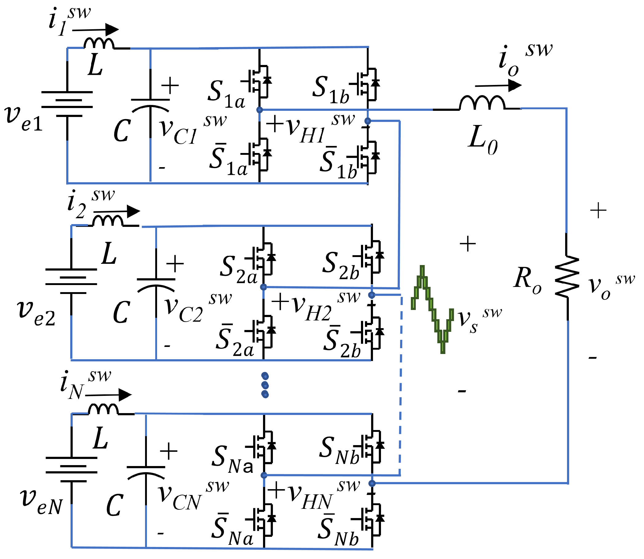
2. Description of the System
This article proposes an adaptation of a decentralized control applied previously to FCMC in [
3,
21], now implemented in a CFBMC of
N Full-Bridges (FBs) with inductive filter and resistive load.
Figure 1 shows the topology of the converter, using MOSFET as the switching device, where the control is implemented.
represents the position of the High-Side switches. It is equal to 1 if the switch of the
kth FB cell is in the ON state and 0 if it is in the OFF state, with
k = 1, 2, …,
N.
y =
a for the left-side branch of the
kth FB cell and
y =
b for the right side.
is the complementary signal of
.
,
,
and
are the input voltage, the switching output voltage, the switching FB cell input capacitor voltage and the switching FB cell input inductance current of the
kth FB cell, respectively, while
and
correspond to the output current and voltage of the inverter, respectively. Depending on the position of the switches, the value of
varies and affects the internal cell signal waveforms. In order to simplify the equations, a slow variation assumption is made by considering the signal frequency is kept low relative to the switching frequency. An average model can be proposed where the variable
x represents the moving average of the
, where
x can be replaced either by
,
,
,
or
. In this work, the objective is to balance the values of the output voltages of the FB cells,
, called the Cell Variable (CV), and to regulate the output current,
, which is the Global Variable (GV). A distributed approach for the control implementation is proposed to provide a way to easily insert or remove an FB cell without adding complexity to the balance control system.
Considering that the outputs of the FB cells are connected in series, the same average current
flows through the output nodes of each FB cell. Therefore, balancing their output voltages is equivalent to balancing the power delivered by each cell. In accordance with
Figure 1, the dynamic equations of the signals of the FB cell are:
where
is the series resistance of the inductance
L and
corresponds to
,
is the drain-source-ON resistance of the MOSFET and
is the series resistance of
.
,
is the duty cycle of
. The modulation strategy used for this converter corresponds to an interleaved unipolar PWM. Therefore,
, producing
. It should be mentioned that because the maximum and minimum values of the duty-cycles are 1 and 0, respectively,
is bounded in
.
The dynamical model of the FB cell output voltage
is:
In accordance with (
1), (
2), (
3) and (
4), the equivalent circuit of the converter is obtained and is shown in
Figure 2:
Considering that, in the CFBMC, all the input voltages
present an identical average value, they can be computed as the sum of a DC component
and a local deviation
. Hence, according to [
12,
30], it is possible to simplify the model, considering that the deviations of the input voltage and the resulting oscillations produced by the input filter operate as a disturbance. Therefore:
where
is the contribution of the filter oscillations on the cell capacitor voltage.
Based on (
3) and (
5), the converter behaves like the presented model:
where
represents the total contribution of the disturbances.
Based on (
6) and (
7),
Figure 3 presents the equivalent linear circuit:
This linear equivalent circuit is simpler than the previous one and takes into account the variations that the input voltages of each cell may present. Because (
6) represents the linear model of the inverter, it becomes possible to express its linear behavior in the Laplace domain:
where
is the Laplace transform of
.
Then, expressing it as a matrix form:
where
,
,
,
.
Finally,
Figure 4 shows the block diagram of (
10) and (
11). It clearly shows that the resulting output current
(s) flowing through the converter inductor is a contribution of the average value of the cell battery voltages
, the disturbances they can produce
(s) and the duty-cycles of the PWM control signals
U(s) applied to the cells.
Thanks to this model, a decentralized controller which is used to balance the output voltage of the cells can be proposed. It is presented in the next chapter.
3. Description of the Decentralized Controller
The control proposed here is based on a local controller described in [
3,
21] for the voltage-cell balancing of an FCMC. Its first application to a grid-tied cascaded multilevel inverter was presented in [
23] where simulations presented interesting results. Here, more investigations are carried out for the implementation of this controller in a CFBMC connected to a resistive load with an inductive filter using isolated input voltage sources per cell, such as batteries.
Figure 5 shows the proposed local control structure.
It comprises two stages, i.e., a Bypass Stage and a Balancing Controller, and receives a global signal computed via the output current regulator.
3.1. The Cell Power Balancing Controller
This stage of the control structure is the cell balancing controller. First, a comparison is made between the value of the FB cell output voltage
with the average value of the output voltages of the neighboring active FB cells,
and
. An error is obtained and then canceled by a linear controller,
. This controller can be either a simple proportional (P) corrector providing constant static balancing errors or a proportional-integrator (PI) canceling the static errors or also a more sophisticated one to address high frequency concerns. A local duty-cycle correction
(s) is obtained as described in (
12). This correction is then applied to the local cell duty-cycle as shown in
Figure 5.
Assuming all the cell controllers carry out the same operation and are connected with their close neighbors in a closed chain of communications, we may expect the system to converge toward the correct balancing of all the cell output voltages, leading to cell power balancing.
This method differs from what is commonly found in the literature, where the average of the output voltage for all the cells is calculated in a centralized way. Here, there is no need for high-speed communication between the cells and a centralized controller.
3.2. The Bypass Stage
The main goal of this block is to manage the communication between the cell controllers depending on their states (active or inactive, enabled or disabled). In accordance with
Figure 5, the cell controller receives an enable signal used to turn OFF or ON the FB cell. When the
kth FB cell is enabled, the bypass system sends the value of the cell output voltage provided by a local voltage sensor
to the neighboring
th and
th cells, respectively. The values of the neighboring cell output voltages
and
are received to compute the local balancing error. When the
kth FB cell is disabled, it is bypassed and the value of
is no longer sent to the neighbors. Instead, the
th and
th cells directly receive the values of
and
, respectively. This bypass stage guarantees the chain of communications is always closed. It allows the insertion or the removal of FB cells easily without adding complexity to the overall control system. This can be done during the converter operation. It should be noted also, if an FB cell is disabled, both High-Side switches
and
are turned on while the others are turned off. This allows the current
to continue flowing through the bypassed cell.
3.3. The Output Current Regulator
This part of the controller regulates the output current supplied to the load. It is a typical linear controller,
, that can be either a classical PI compensator or any type of regulator depending on the specifications of the application in terms of bandwidth, transient step response and stability criteria. Its design is based on the knowledge of the open-loop transfer function of the system considered. In accordance with
Figure 5, the signal
provided by the output current regulator, which represents the main duty-cycle of the system, is defined as:
In accordance with (
12) and (
13) and
Figure 5, the local corrected duty-cycle signal of the FB cell is defined as:
It is important to note that only one output current regulator is present in the system. Its output signal is shared among the converter FB cells to obtain the local corrected duty-cycle signals .
The control method illustrated in
Figure 5 is applied to each FB cell. Then the cells are connected together in a closed-loop chain of communications to exchange with their close neighbors the values of their output voltage. The resulting control scheme is shown in
Figure 6.
A global output current loop is present to regulate the current delivered to the load. It computes the value of the duty-cycle applied to the FB cells connected in series. Thanks to the interleaving of the PWM signals obtained, an apparent frequency equal to N times the switching frequency is observed at the output and reduces the inductor current ripple. This helps to decrease the value of the converter inductor for a given current ripple constraint. The cell controllers compute local corrections , add this correction to the main duty-cycle value and produce a local corrected duty-cycle to balance their own cell output voltage with those of their neighbors. They are all involved in a closed-loop chain of communications.
Notice that the Nth cell communicates with the first and the ()th cells and the first cell communicates with the second and the Nth ones, closing the chain of the communications.
Expressing (
15), for all the values of k,
as a matrix form, it follows that:
where
The local duty-cycles are then a contribution of the computation result of the global current loop, dependent on the difference of the converter output current and the current reference imposed by the user and the local correction balancing the FB cell output voltages dependant on the isolated input cell voltage mismatches. It should be noted that the matrix represents the topology of the interconnections put in place to help the cell controller to compute its duty-cycle correction, i.e., communicating only with their close neighbors. This matrix is circular and has the advantage of being easily diagonalizable. It will help to determine the different responses of the modes presented by this balancing method.
4. Closed-Loop System Analysis
This section is dedicated to the mathematical study of the closed-loop system using the proposed controller. An analysis of the closed-loop transfer functions which comprise the output current regulator and the local balancing controller makes it possible to determine the nature and the appropriate parameters of the controllers used. Their design is discussed in the next chapter. The block diagram of the system including the linear model of the converter with the controllers is shown in
Figure 7.
Compared to the one of
Figure 4, it can be seen that two control loops have been added, i.e., the output current regulation loop using
and the FB cell output voltage balancing loop using the corrector
. Because the converter implements several cells, the system is a matrix. The vector
represents the voltage deviations from the value
which may exist on the input voltages of the cells. It acts as a disturbance input vector and the resulting vector
represents the corrected duty-cycles of the cells.
Thanks to
Figure 7, both the open-loop and the closed-loop transfer functions of the output current regulation loop and the ones of the cell output voltage balancing loops can be determined. They are necessary to determine the appropriate parameters of the correctors for a desired bandwidth and to ensure the system stability.
4.1. Output Current Regulation Loop Analysis
To design the output regulator, it is necessary to determine the output current regulation loop transfer function. Inserting the decentralized controller expression proposed in (
16) into the model of the output current control loop of the inverter and taking into account that
and
in (
10), one obtains:
where
and
is the open-loop transfer function of the output current regulator.
Notice that the term related to the balancing control stage is removed in the transfer function
because
represents the Laplacian of a graph. Indeed, according to [
3,
21,
23], the sum of its elements of the rows and the sum of its elements of the columns is zero. Because this matrix is post multiplied by
, the results are zero. Based on
, the design of
is provided in the
Section 5.
In order to obtain a better understanding of the influence of the balancing control loop on the output current
, it is necessary to analyze the closed-loop transfer function of the output current regulation loop,
, which is defined below.
This shows that the resulting regulated output current is provided by the separate contribution of the current loop and that of the cell input voltage disturbances via the transfer function . Indeed, disturbances on the cell input voltages imply cell voltage mismatches and generate also slightly damped oscillations on the cell capacitors due to the second-order filter LC. Temporary variations appear on the cell local duty-cycles, generating output current transients.
For the following analysis of the control loops, it should be considered, if the output regulator is well designed, when is a step, at means that with , , producing when .
4.2. Cell Voltage Balancing Control Loop Analysis
Now, the balancing control loop has to be analyzed inserting (
16) in (
11); it follows that:
Inserting (
18) into (
19), one obtains:
Then, the expression is simplified and an open-loop transfer function is considered by inserting an excitation signal on the cell output voltages:
where
is the excitation signal.
One can see that the FB cell output voltages are dependent on the current reference value and the input voltage disturbances . The voltage balancing open-loop transfer function is then identified.
The controller
will be defined in the
Section 5 based on the desired bandwidth of
, which is directly linked to the eigenvalues of the matrix
.
4.3. Global Closed-Loop Analysis
In accordance with (
17) and (
19),
Figure 8 shows the simplified closed-loop block diagram.
This block diagram of the closed-loop system is similar to the one presented in
Figure 7, but the two loops, i.e., the output current regulation loop and the cell output voltage balancing loop, are presented separately. This is possible because the vector
is made of the sum of a constant term
and a disturbance. This helps in considering the separate contributions of the disturbances on the two closed-loop systems involved.
Notice that the FB cell voltage vector
depends on three inputs; one corresponds to the balancing controller, another depends on the disturbance,
, and the last one depends on the output current loop, which affects all the cell voltages at the same time. Analyzing in steady state, in accordance with (
21), when
, if the controller is well designed,
, entailing that the trajectory in steady states for
is
.
5. Design of the Controllers
Now, both controllers have to be designed, taking into account some criteria, such as the bandwidth of the loops and the stability of the overall system.
5.1. Design of the Output Current Regulator
Based on , for a stable and low bandwidth system, a simple integral corrector can be proposed for . Then, the static error between and is canceled and the stability is ensured by considering the open-loop transfer function phase margin.
Because the chosen controller type for the output current regulator is an Integral (I) controller:
The Bode analyses of
,
and
are shown in
Figure 9, where
correspond to the natural response of the converter.
At low frequency, with , the module of the open-loop transfer function presents a slope of −20 dB/decade. That its to say, its phase is equal to −90°. At high frequency, with , due to the pole provided by , a slope of −40 dB/decade is obtained, which corresponds to a phase close to −180°. In order to guarantee a sufficient phase margin, i.e., more than 60°, for stability purposes, the bandwidth has to be less than half of .
Considering
Figure 9, it becomes possible to determine the value of the corrector parameter
for a given bandwidth
. It follows that:
where
is the bandwidth of the output regulator.
In practice, is fixed ten times less than the switching frequency of the MOSFETs, .
5.2. Design of the Cell Voltage Balancing Controllers
The cell voltage balancing controller is designed based on the
expression. In accordance with (
21),
is proportional to the matrix
. Then, the study of the eigenvectors of this matrix makes it possible to replace it by a diagonal matrix whose terms reveal its eigenvalues. Decomposing
in a diagonal matrix leads to:
where
is a diagonal matrix and
is the eigenvector of
.
Consequently, the open-loop transfer function of the cell output voltage balancing system can be expressed on a new basis where the vector
is deduced from the excitation vector
using the diagonal matrix
. It should be noted that one eigenvalue of
is equal to 0, because it is a Laplacian of a graph.
represents the transfer function of the modal responses of the balancing system, defined as:
where
.
Finally, on this new basis,
N modes exist and have to be studied. The open-loop transfer function
of the
kth mode is:
It should be mentioned that
corresponds to a circulant matrix
, which is described as:
Since
is a circulant matrix, it is possible to obtain an expression of its eigenvalues. According to [
31], the eigenvalues of a circulant matrix are:
where
.
It can be observed that for the case of the matrix
, the coefficients,
s, are:
Therefore, in accordance with (
33) and (
34), the eigenvalues of
are defined as:
Notice that the first eigenvalue, , is equal to 0, validating that it also represents the Laplacian of a graph. corresponds to the common mode of the balancing system. This mode is only influenced by the output current regulation loop which imposes the average value of the cell output voltages. Furthermore, because of the symmetric property of the cosine, the kth eigenvalue is equal to the th eigenvalue. Finally, the highest eigenvalue is obtained for when N is even and when N is odd. The maximum case is produced when N is even, generating . For odd values of N the highest eigenvalue tends to be 4 when N increases. The design of the balancing controller is based on the possible maximum eigenvalue, , and the minimum eigenvalue, , whose values are 4 and 0, respectively.
means the system presents a pure integrator that theoretically is stable. However, due to numerical approximations in the implementation, the system may diverge after a long period of time. For that reason, the selected controller corresponds to a low-pass filter that ensures the stability of the system, with a pole located at low frequency. Hence, the proposed controller is:
In order to determine the parameters of the controller,
Figure 10 shows the Bode diagram of
,
and
, respectively. The higher the value of
, the higher the bandwidth of the mode. Consequently, the maximum value of
is considered, i.e.,
. The proportional term of the low-pass filter
is determined by the maximum tolerated accuracy for the balancing of the cell output voltages. Then, as shown in the Bode diagram of
Figure 10, the bandwidth
is set using the
parameter:
In order to avoid any interference between the loops, the bandwidth, , must be ten times less than the bandwidth of the output current regulation loop, . Stability is guaranteed because the phase of the open loop function is always greater than or equal to −90° leading to a phase margin greater than 90°.
5.3. Modal Response Simulation
The simulations are performed with a 5-FB cell CFBMC, using 48V batteries. The parameters of the application and the ones of the controllers are shown in
Table 1.
The objective here is to observe the modal response of the voltage balancing loop. For
,
corresponds to:
Appendix A shows the demonstration of these values; their numeric values are:
while the modal matrix,
, is:
Using the eigenvectors as the initial conditions,
Figure 11 shows the modal response of the system.
It is clearly observed that the system is stable and the time responses of the modes are very different. Depending on the parameter
of the decentralized controller, this time response can be adjusted.
Table 2 shows a comparison between the theoretical time constants and the ones obtained via simulation.
It should be noted that, since there are two pairs of similar eigenvalues, there are also two pairs of time constants, which means that there are two double poles for each time constant. Furthermore, it can be observed that simulated and theoretical values are very similar, validating the performance of the controller.
6. Simulations and Experimental Results
Both simulations and experimental results, developed hereafter, are obtained with the converter working as a DC/AC converter, with three different tests: an input voltage step, a load step and a cell insertion during operation.
6.1. Full System Simulation Results
The simulations are developed in Simulink with SimPowerSystem tool, with sampling frequency of
. The solver algorithm used ODE23tb(stiff/TR-BDF2), which is a differential equation solver method for Stiff equations that use the trapezoidal rules with a backward differential formula of second degree. The first simulation test corresponds to a load transient from 95
to 70
.
Figure 12 shows
and
when the converter works as a DC/AC converter.
It is observed that before the disturbance occurs, the multilevel converter uses nine voltage levels. After the disturbance, only seven levels are required to regulate the output current. Notice also that the CVs are balanced throughout the simulation, before and after the disturbance, validating for DC/AC conversion that when a disturbance in the output current occurs, the CVs are not unbalanced; only their common average value are affected. Furthermore, the current is stabilized during a small transient, less than 1 ms.
The next simulation result, shown in
Figure 13, corresponds to an input cell voltage disturbance, i.e., a step voltage from 40 to 50 V for the inverter with a resistive load of 77
.
It should be noted that the voltage disturbance almost affects neither the output current
nor the output voltage
, while the CVs are automatically balanced thanks to the decentralized controllers in only 0.5 ms.
Figure 13 also shows that, by the nature of the inverter, when one of the input voltages is 40 V, there exists an asymmetric ripple in
and
and when the input voltage is 50 V, the ripples are equalized. However, in both cases the average output current
and the
s are well regulated and balanced, respectively.
The next simulation corresponds to a cell insertion during operation, going from 4 FB cells to 5 FB cells, when the converter operates as an inverter.
Figure 14 shows the results obtained for the
s,
and
signals.
It should be noticed that before the cell insertion, both and present a high ripple, due to a constant control signal interleaving set for five cells, i.e., signal phase. Even if the ripple is high, the average value of the output current is regulated when only four cells are activated. When the fifth FB cell is inserted, presents an overshoot and then it is stabilized in less than 0.25 ms. voltages are balanced when there are four FB cells and then, when the fifth cell is inserted, they are auto balanced, reaching a new operation point in 0.25 ms approximately.
This test validates via simulation the three functions of the controller, the balancing of the CV, the regulation of the GV and the bypass system activation. It can be inferred that all the simulation results are in concordance with the previous theoretical study, producing the expected behavior in terms of reconfigurability, bandwidth and stability for this multilevel converter topology.
6.2. Experimental Results
The five-cell CFBMC is implemented in a laboratory prototype, as shown in
Figure 15, with the parameters described in
Table 1. It is fed by five 48 V Li-ion batteries. The switching device used in the FB cells is the IRFI4212H MOSFET. Voltage is read with the AMC1200 differential amplifier and current with the ACS714 Hall effect sensor. The control algorithm runs in a LAUNCHXL-F28379D development board. The measurements are carried out with an MSO-X 4034A oscilloscope, using N2783B and N2790 probes for current and voltage, respectively. More details related to the construction of this inverter are presented in [
32].
In order to compare the simulation and experimental results, the tests developed here are the same as the ones illustrated in the previous simulations.
Figure 16 shows the experimental results of the first test, corresponding to a load step (or load transient). It can be seen that there exists a concordance with the simulation results of this test, presenting similar overshoot in the current and similar settling time. Moreover, the switching levels of
are the same. Furthermore, as happened in the simulation, the operating points of
s change in 0.5 ms without any unbalance between them.
The next result corresponds to the disturbance in one input voltage FB cell.
Figure 17 shows the behavior of the output current
, the output voltage
, the switching output voltage of each FB 1, 4 and 5,
,
, and their respective moving average,
s.
It should be noted that the step voltage is almost not detected in s. This is because the input filters presented in the converter smooth the effect of the voltage disturbance. Furthermore, it can be observed that during all the experiments voltages are well balanced. This observation also validates the balancing controller, maintaining the same output voltage of each FB cell even when the input voltages change. Additionally, the output current is well regulated.
The next result, presented in
Figure 18, corresponds to an FB cell insertion during operation, starting with four FB cells and inserting the fifth FB cell. It is important to note that the current follows the reference during all the experiments, presenting a small transient when the FB cell is inserted. Furthermore, it can be observed that the CVs are well balanced after the insertion, reaching a new operating point with a settling time of 0.6 ms, approximately. These values are in concordance with the predicted time constants of the system and show a strong similarity with the simulation results. This test validates the three stages of the controller, the balancing controller, the GV regulator and the bypass system.
It can be inferred that all the experimental tests are in concordance with the simulation tests and the theoretical studies developed in this paper, demonstrating the good performance of the controller for this topology.
7. Conclusions
A decentralized control method for balancing the power delivered by the cells of a cascaded full-bridge multilevel converter has been presented. It associates a controller for each full-bridge cell that communicates with its neighbors to balance the output cell voltages, making unnecessary the calculation of the average voltage value with a centralized controller.
The presented work gives to the cascaded full-bridge multilevel converter the ability to reconfigure by inserting or removing cells during operation without complicating the control architecture, which is valuable for systems integrating functional safety in the event of hardware faults. This characteristic also offers the option to easily set the number of cells to be used to track the converter maximum power efficiency, as a function of the load power.
Simulations and experimental results, with a five-cell converter, demonstrate robust and stable operation, guaranteeing the balance of the powers delivered by the cells, against load step transients, battery voltage disturbances and cell insertion.
Due to its modularity, this control method can manage any number of cells, making it viable for applications where several sources need to contribute with the same amount of power to the load, as might be the case with solar panels in a farm or batteries in energy storage systems or even any other power converter with multi-sources that must deliver the same amount of power, and, moreover, in high power applications where efficiency could be improved by using low voltage devices.
Future work is planned for balancing the state-of-charge of battery cells using a similar distributed control method. Moreover, a sensitivity analysis will be carried out to test the robustness of the system against the variability of the parameters.


