Article

T-NPC Soft-Commutated Inverter Based on Reverse Blocking IGBTs with the Novel Concept of a DESAT Control Circuit in the Gate Driver

Department of Power Electronics and Energy Control Systems, Faculty of Electrical Engineering, Automatics, Computer Science and Biomedical Engineering, AGH University of Science and Technology, al. Mickiewicza 30, 30-059 Krakow, Poland
Energies 2023, 16(12), 4642; https://doi.org/10.3390/en16124642
Submission received: 30 March 2023 / Revised: 7 June 2023 / Accepted: 8 June 2023 / Published: 11 June 2023
(This article belongs to the Section F3: Power Electronics)

Abstract

:
This article presents the concept of switching and conduction loss reduction in a T-NPC inverter based on IGBT transistors. The method of limiting switching losses involves the connection of an LC circuit designed to cause transistors in vertical branches to shut down under zero voltage conditions. In order to reduce conduction losses, it was proposed to use two reverse blocking transistors connected anti-parallel in the horizontal branch of the inverter. To ensure safe operation of the transistors, a gate driver proposal for controlling the IGBT reverse blocking transistor is presented. The solution is characterized by a changed part of the driver, responsible for short-circuit protection. It eliminates excessive, destructive currents that can potentially flow through the driver circuit under the influence of the power supply voltage of the power circuit connected backwards to the controlled transistor. Examples of applications and benefits of the proposed solution are presented and verified with laboratory tests.

1. Introduction

NPC (Neutral Point Clamped) converter systems have been developed over the years for implementation in high-power converter systems [1,2]. One of the favorable NPC topologies is the concept of a T-NPC system, which is characterized by a small number of semiconductor devices [3]. These topologies are also the subject of intensive research and, in several publications [4,5,6,7,8], certain research problems related to the implementation of T-type NPC inverters in photovoltaic systems [4,5], in high-power traction systems, and in rectifier systems [7,8] were presented.
Power electronics is an area of engineering that seeks new methods which convert electrical energy in order to maximize efficiency. Solutions often lead to a reduction in switching losses in power transistors. In terms of reducing conducted losses, an improvement was achieved with the use of appropriately selected components. Reducing conduction losses along with the elimination of the number of transistors in the system may be achieved by using reverse blocking IGBTs (RB-IGBTs) in certain topologies [9]. They can be used where a controlled unidirectional current flow is required, and no anti-parallel diode (body diode) is needed. The concept of RB-IGBT modules is still being developed. In [10], the novel concept of an IGBT with bidirectional blocking capability with improvement in Eoff and Von reduction was demonstrated, and in [11] the novel concept of N-channel RB-IGBT with low energy losses and a simplified fabrication process was proposed.
Among the known systems, RB-IGBT devices can be used in current-source inverters, matrix converters, modular multilevel converters (MMC), and in the horizontal branch of the T-NPC voltage inverter. Such solutions eliminate the diode which conducts current in a vertical branch together with a transistor, and thus the conducted losses in the inverter are reduced. Publications [12,13,14,15] presented concepts and results of research on MMC with RB-IGBT transistors. One of the research problems still being analyzed in this type of system is DC Fault Ride-Through. The use of reverse blocking branches simplifies the control and application of industrial MMC. In [16], current-source rectifiers with RG-IGBT implementation were demonstrated. The publication [17] presented a three-phase T-type inverter based on RB-IGBT where high efficiency (98% at 15 kW output power and 600 V input voltage) was achieved, and in [18] a five-level inverter with a bidirectional blocking branch in its structure was analyzed.
The application of RB-IGBT can allow a decrease in power losses in T-type inverters, while the efficiency can be further improved using the soft switching technique. The analysis of IGBT soft turn-off, power losses, and switching processes was presented in [19]. In the case of systems with IGBTs, the amount of energy dissipated during its turn-off can be significant; that is why many concepts for reducing turn-off losses appear. Publications [20,21,22] presented the results of research on a T-NPC type inverter in soft turn-off obtained by using a passive auxiliary switching circuit. The efficiency results presented in [21] positively verified this concept of modification of the three-level T-NPC inverter. In [22], the improvement of the operation of this converter via additional control functions was presented. This system was optimized by using a different, active resonant cell, as presented in [23]. In this system [23], no load current flows through the resonant choke, which reduces its volume. The concept of limiting switching losses by using active commutation circuits can also be found for two-level inverter systems, an example of which is the inverter presented in [24].
Reverse blocking transistors (RB-IGBT) can be controlled using classic drivers. For this type of transistor, however, driver solutions are developed to improve the performance of the transistor. In [25], a gate driver solution was presented to optimize the switching dynamics of the RB-IGBT, which may be worse than those of a classic IGBT. In the case of IGBT transistors, the driver usually has an additional function to protect the transistor against short circuit (DESAT control). The use of classic drivers with a protective function for reverse blocking transistors connected in parallel is impossible, due to the flow of current caused by the supply voltage of the power circuit through the diodes of the driver control circuit. Various methods are used to limit this effect [26,27,28,29]. In [26,27], UCE voltage detection for the collector’s overcurrent protection used a sensing circuit with a large resistor. This new method was implemented in the new driver project demonstrated in [26,27]. In [28], the concept of modifying the driver protection circuit for RB-IGBT by using resistors and an additional diode implemented with the standard driver was presented. In [29], a concept for a protection system was demonstrated where the CPLD-based circuit managed different categories of IGBT faults.
Publication [30] presented a short-circuit current protection solution in a gate-driver circuit that can also work with a standard IGBT driver. In the solution presented in [30], the DESAT control circuit was activated when the power transistor was switched on. Preliminary analyses of the concept show that it can be very effective, but its application requires verification based on research, which is presented in this article. The results of the research contained in this article include the analysis of T-type three-level inverter systems, with the RB-IGBT transistor implemented.
Overcurrent protection and soft switching operation allow a decrease in the temperature stress of an IGBT switch, which may improve the reliability of a converter. Distribution of failure is the subject of research in multilevel NPC inverters. In [18], there is detailed research of reliability and failure issues in relation to a five-level inverter, where a T-NPC part was used. The issue of the reliability of IGBT transistor-based modules is also the subject of separate studies, as demonstrated in publications [31,32,33,34,35]. In [35], there is an analysis of the factors influencing the failure rate of the IGBT modules. Overcurrent and thermal parameters are important factors that are associated with the DESAT protection implemented in a gate driver.
Contributions to the article include proposing a driver that works with IGBTs and, in particular, RB-IGBTs and making an analysis of a resonant circuit to support the turn-off of transistors in a T-NPC inverter. The driver ensures the effectiveness of the short-circuit protection (DESAT protection) and does not allow, compared with the classical driver application, the flow of destructive current through the DESAT sub-circuit. As a result, it is possible to use RB-IGBT with full protection, for instance, in the horizontal branch of the T-NPC inverter with the RB-IGBT connected in anti-parallel. Such a solution makes it possible to reduce the conducted losses of the system. The driver proposal has been granted several patents. In terms of minimizing switching losses, the use of an additional resonant circuit is presented. The analysis of this circuit was carried out and the criteria for the selection of its parameters were determined.
The article also contains numerous experimental results, giving the possibility to verify the operation of the driver system in the three-level T-NPC type inverter. The setup used in the research allowed us to compare the operation of the inverter system in three configurations, namely the classic system, the inverter with anti-parallel reverse-blocking transistors, and the resonant inverter, which is also included in the article.
The organization of the article is as follows. Section 2 describes a concept for the T-NPC inverter in a topology with auxiliary circuits for soft turn-off as well as the analytical consideration of this circuit. In the same section, a concept for the proposed gate-driver for RB-IGBTs is addressed. The operation of the inverters is verified by experiments, which is presented in Section 3 along with the experimental results.

2. T-NPC Inverter Cases of Implementation for Power Loss Reduction and DESAT Control Circuit in Gate Driver

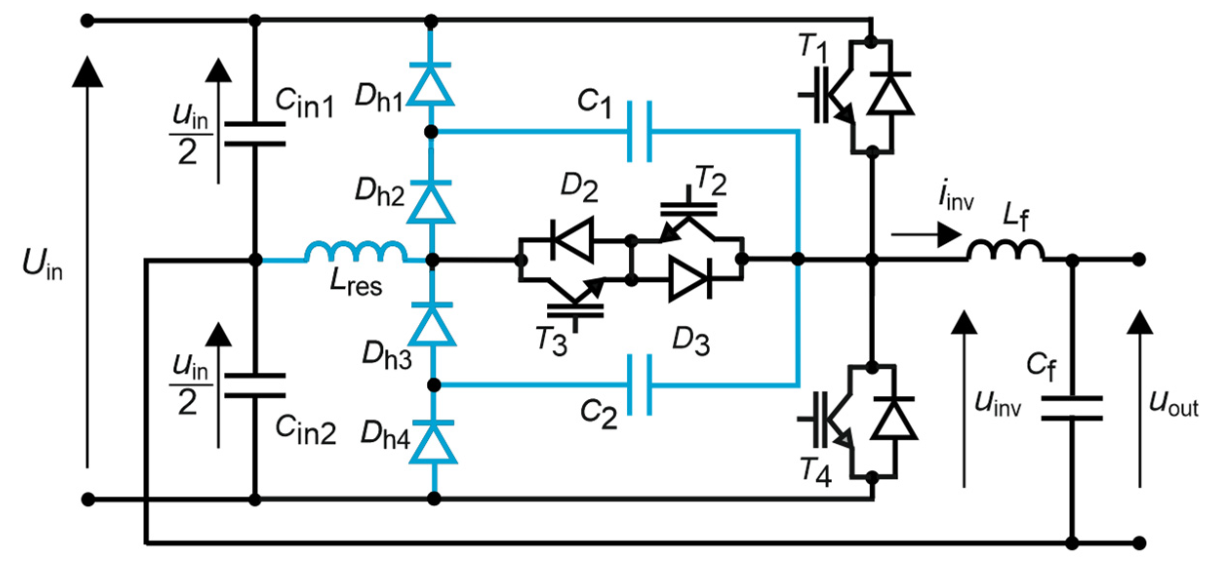
2.1. T-NPC Inverter in Soft Switching Configuration for the Reduction of Switching Losses

The T-type topology can be supported with a soft switching cell according to the concepts shown in Figure 1 (S3L converter) and published in [15,16,17,18]. In the S3L converter, turn-off losses can be significantly reduced, which is favorable for IGBT-based converters. An auxiliary commutation cell (ACC) of the S3L converter was built of capacitors and diodes in the circuitry, which delayed voltage rise on the transistor during its turn-off process. An additional inductor as used for charging the ACC capacitors.
The process of current commutation in the ACC occurs in several stages which contain charging or discharging of the auxiliary capacitors. Figure 2 presents the results of simulations carried out in the Matlab Simulink, which show the idea of the S3L converter operation.
During the turn-on process (stages F, G in Figure 2) of the transistor in the vertical branch (e.g., T1), the auxiliary capacitor C2 is charged from the upper dc-link capacitor connected in series with the resonant inductor (Cin1, T1, C2, Dh3, Lres). In the case when the commutation of the load current from the upper transistor of the vertical branch to the horizontal branch occurs, the auxiliary capacitor C2 discharges (stages B, C, and D in Figure 2). After the vertical switch T1 is turned off, the current flows via the lower capacitor C2, causing its discharging. The rate of voltage decrease across the C2 capacitor determines the rate of voltage rise across the transistor during its turn-off process. At the same time, the current on the auxiliary choke rises and the process of commutation finishes when the current flows via the horizontal branch and the auxiliary choke. The turn-off losses on the vertical switches can be significantly decreased.
A detailed concept and operation of the S3L converter was presented in [15]. In [16,17,18], further issues associated with the S3L converter such as the dead-time, EMC, efficiency, and other solutions were analyzed. An analytical consideration of the ACC is included in the next section.

Analytical Consideration and Selection of the S3L Parameters

When transistor T1 is switched on (Figure 1), capacitor C2 is charged in the oscillatory circuit composed of the following devices: Cin1, T1, C2, Dh3, and Lres. For zero initial current of the Lres choke, non-zero initial voltage across the capacitor, and zero resistance (no damping) of the charging circuit, the choke current Lres and the voltage across capacitor C2 are as follows:
i L r e s t = 1 2 U i n U 0 ρ c h sinω ch t
u C 2 t = 1 2 U i n + U 0 1 2 U i n cosω ch t
where iLres [A] is the choke Lres current, uC2 [V] is the voltage across capacitor C2, Uin [V] is the system supply voltage, U0 [V] is the initial voltage across capacitor C2, ωch = (LresC2)−0.5 [rad/s], and ρch = (Lres/C2)0.5 [Ω] is the pulsation and wave resistance of the capacitor C2 charging circuit.
The charging time of capacitor C2 is equal to half of the overcharge period of the resonant circuit. In order to maximally charge capacitor C2 in any case, this time interval should be shorter than the shortest conduction time of transistor T1:
t c h = 1 2 T c h = π L r e s C 2 < t T 1   O N
where: tch [s] is the charging time of capacitor C2, Tch [s] is the overcharge period of the resonant circuit, and tT1 ON [s] is the conduction time of transistor T1.
Assuming zero initial conditions, after the charging time there is maximum voltage across capacitor C2:
U C 2 m a x = U i n
Capacitor C2 is discharged in the circuit composed of the devices: Cin2, Dh4, C2, Lf, and the load. The initial value of the discharge current is Iload max. Due to the high value of the output filter inductance Lf and the possible inductance of the load, the oscillating discharge period (ωdis = (LfC2)−0.5) is significantly greater than the time required to fully discharge capacitor C2. For this reason, it should be assumed that capacitor C2 discharges linearly with the load current:
d u C 2 d t = I l o a d   m a x C 2
where Iload max [A] is the maximum value of the load current.
The discharge time of capacitor C2 should not be longer than the non-conduction time tOFF of transistor T1 and not shorter than its turn-off time toff.
t T 1   o f f t d i s = π L f C 2 t T 1   O F F
where tdis [s] is the discharging time of capacitor C2, tT1 OFF [s] is the non-conduction time of transistor T1, tT1 off [s] is the turn-off time of transistor T1, and Lf [H] is the inductance of the filter choke.
During the toff turn-off of transistor T1 at the maximum load current Iload max, the voltage across capacitor C2 should decrease by no more than the assumed ΔU. Then, the minimum capacitance value of the capacitor is defined as:
C 2 m i n = I l o a d   m a x t T 1   o f f U C 2
If capacitor C2 is charged to the maximum voltage UC2max and during the non-conduction of transistor T1 the load current is minimum Iload min, then to ensure its discharge to zero, the capacitance value should not be greater than the following limit:
C 2 m a x = I l o a d   m i n t T 1   O F F U i n
In fact, the minimum value of the inverter’s load current is zero at the beginning and the end of each half-period. This allowed us to assume that switching losses were negligible. Therefore, it is necessary to determine the minimum value of the load current for which (8) will apply. For smaller current values, capacitor C2 will not be fully discharged.
The charging current of capacitor C2 is added to the load current flowing through transistor T1. Assuming the maximum value of the collector current IT1 max of transistor T1, for the maximum load current Iload max the minimum value of the inductance of the resonant choke is:
L r e s   m i n = C 2 1 4 U i n 2 I T 1   m a x I l o a d   m a x I l o a d 2
where ΔIload [A] is the ripple of the current load.
The maximum value of the choke inductance Lres is derived from the oscillation charging time of capacitor C2 and the minimum conduction time of transistor T1:
L r e s   m a x = t T 1   O N   m i n 2 C 2 π 2
The amplitude of the current that charges capacitor C2 is:
I C 2   m a x = U i n 2 ρ c h = U i n 2 C 2 L r e s
while the current of the resonant choke is the sum of the load current during the conduction time of the inverter’s horizontal branch transistors and the charging current of capacitors C1 and C2.
Analogous charging, discharging, and capacitance selection conditions for the capacitor C1 occur in the negative half-period of the output voltage.
The currents of diodes Dh3 (Dh2), Dh4 (Dh1) are the same as the charging and discharging currents of capacitor C2 (C1), respectively. The maximum voltage across diodes Dh3 and Dh2 is on the level of Uin/2, while the voltage stress across diodes Dh4 and Dh1 is Uin.

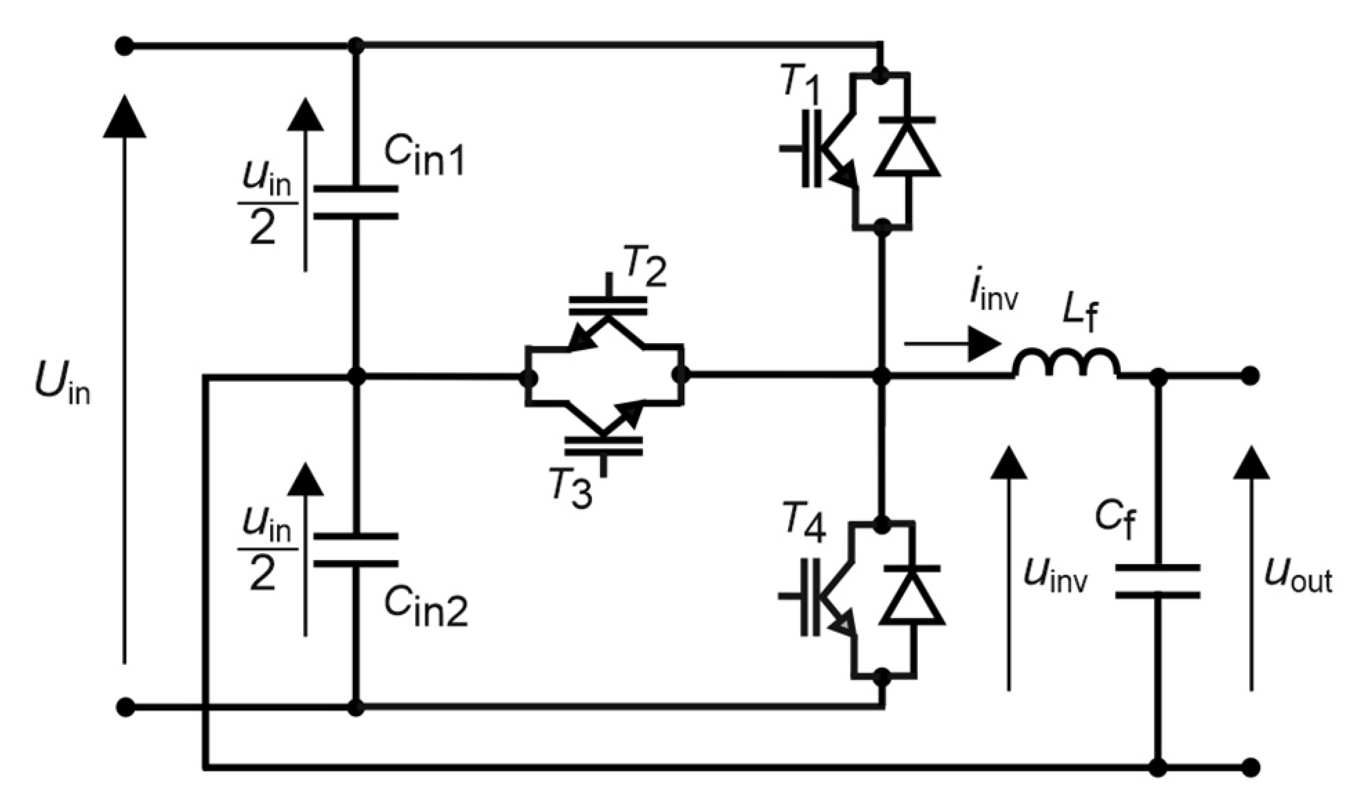
2.2. Reduction of the Conducted Losses in a T-NPC Inverter

In the most commonly used solutions, two anti-series connected transistors in the horizontal branch of the T-NPC inverter are used. This ensures controlled current flow in both directions. In this case, the current in the horizontal branch flows through two semiconductor elements—a transistor and a diode in each direction
In a T-NPC inverter, it is possible to reduce the number of semiconductor devices used in the horizontal branch with the use of two reverse-blocking IGBT transistors connected in anti-parallel. Figure 3 shows such a circuit with input capacitors and an output filter. The flow of current in both directions is still controlled, and two diodes are eliminated from the system. Thus, it is possible to reduce system losses by conducted losses of diodes.
In the proposed solution, as well as in other similar ones with reverse-blocking transistors (without body diode), where there is a higher voltage potential on the transistor emitter than on its collector, it is not possible to use a classic gate driver with short-circuit protection (DESAT). In order to maintain full protection, a suitable solution is proposed in in the next section.

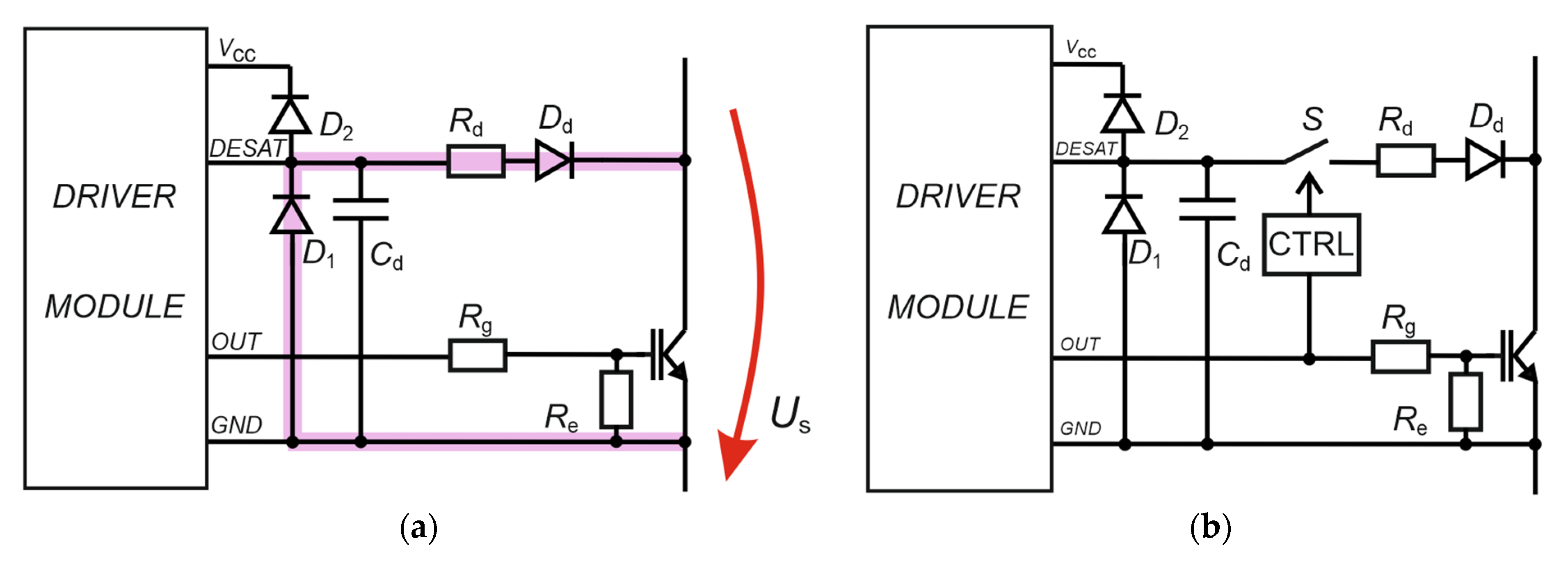
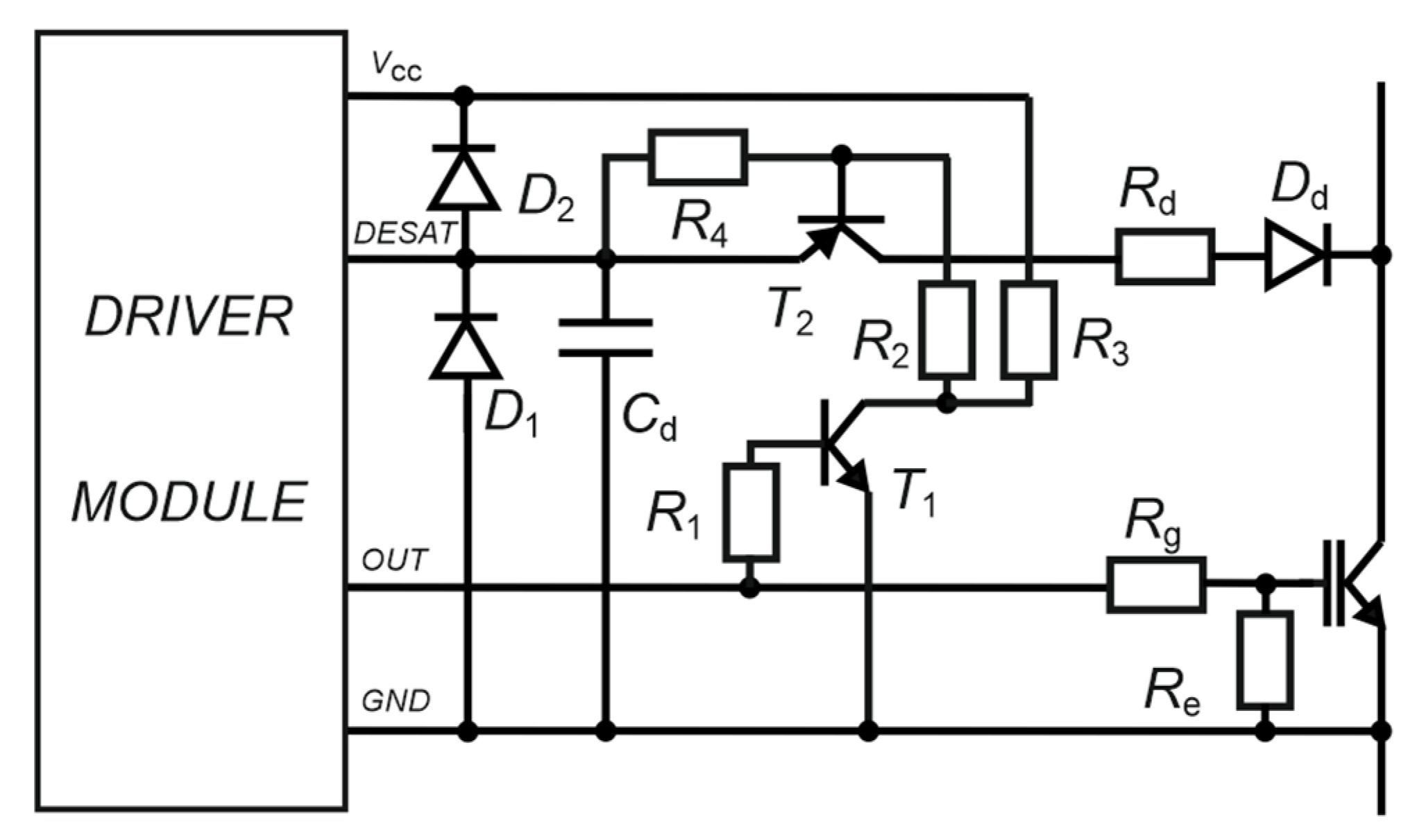
Driver with DESAT Control for Anti-Parallel Connected Reverse Blocking Transistors

Figure 4 shows a functional diagram of the classic and the author’s proposed gate driver of an IGBT transistor [30] with applied power transistor short-circuit protection (DESAT control). The circuit in its basic form consists of a gate resistor Rg; short circuit protection elements Cd, Rd, Dd; and diodes D1, D2. The diodes D1, D2 are necessary to protect the internal DESAT circuit of the driver module. In some models they are found inside the driver IC.
In case of a higher voltage potential on the emitter of a power transistor in the classic driver, there will be a current flow from the ground potential of the driver through the protection diode D1, resistor Rd, and diode Dd of the DESAT circuit (Figure 4a). This current will be practically limited only by the resistance of the resistor Rd. It is usually 100–1000 Ohms and depends on the IC used. For a voltage occurring at the power transistor of several hundred volts (for example, in an NPC inverter), the current flowing through the DESAT circuit could have a value of up to several amps which is destructive for the circuit.
The operation of the proposed driver circuit, according to the concept presented in [30], for switching on and off the IGBT power transistor is the same as any classical one. The difference lies in the operation of short-circuit protection. To eliminate the possibility of a large current flowing through the circuit, the protection circuit is switched on only for the duration of the power transistor’s operation. This is performed by the S switch (Figure 4b). It can be controlled by a gate signal through the corresponding sub-circuit. The switch was used between the driver IC and the high-voltage diode Dd so it could be, for example, a low-voltage transistor. The whole modification is therefore not expensive or problematic. An example of the implementation of the proposed driver is shown in Figure 5.

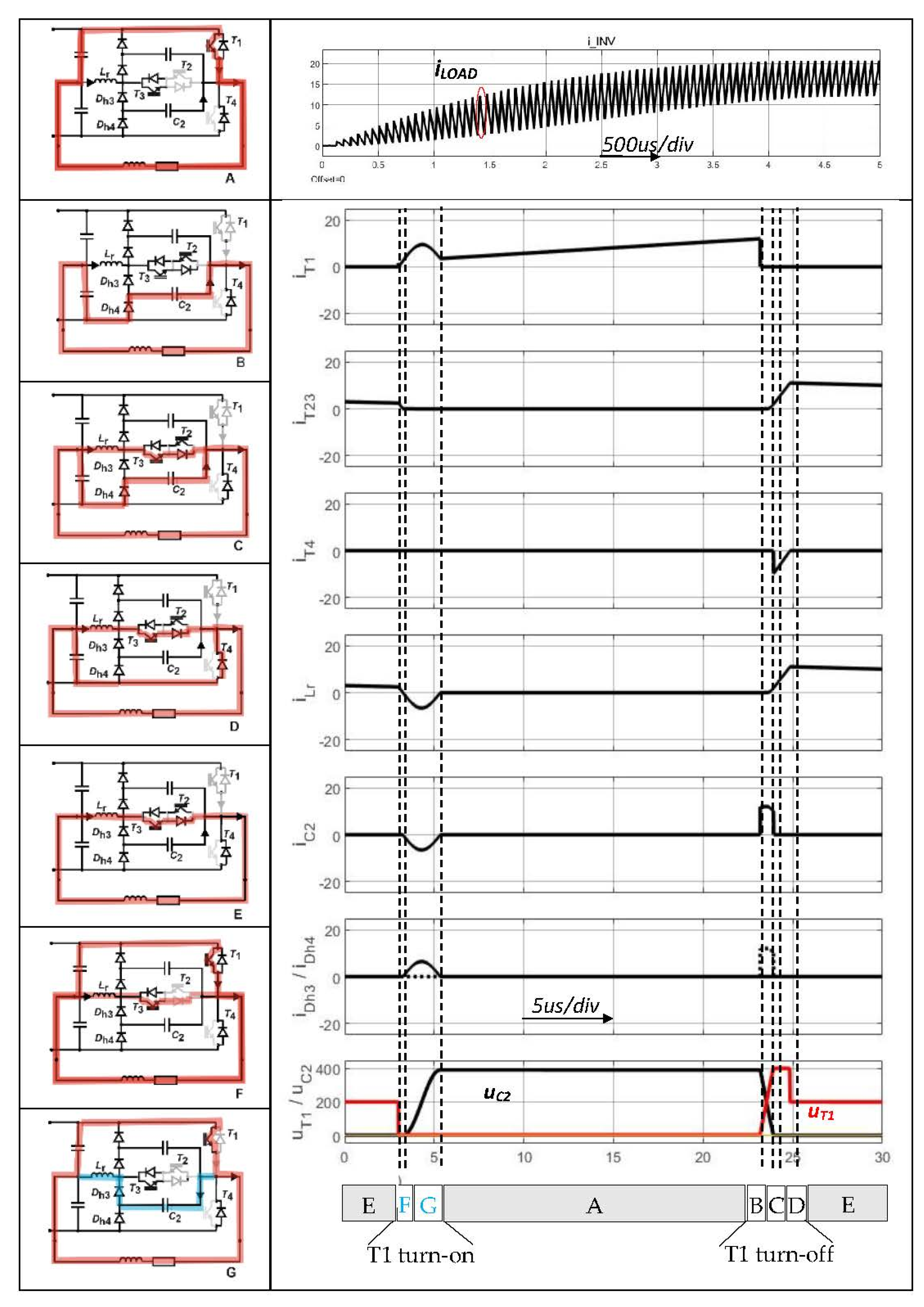
3. Experimental Results

3.1. The Laboratory Setup

In order to verify the proposed concepts, laboratory tests were carried out. Three T-NPC inverter circuits were created which contained:
-
the classic inverter with a horizontal branch consisting of anti-series connected IGBT transistors with reverse body diodes;
-
the inverter with a resonant circuit added, according to Figure 1;
-
the inverter with anti-parallel reverse-blocking transistors in the horizontal branch (Figure 3).
Figure 6 exhibits the laboratory setup of the inverter with anti-parallel reverse-blocking transistors in the horizontal branch. The circuit contains transistors placed on a heatsink, complete drivers with a secondary-side power supply, and supporting input capacitors. For the horizontal transistors, the driver proposed was applied (according to Figure 5). The transistors were controlled by an external control system based on Intel Cyclone V. The classic inverter and S3L were very similar and are made in the same way. The PCB has different power tracks in the horizontal branch and the classic drivers were used. The S3L (according to Figure 1) was based on a classic T-NPC inverter with the added LresC1(C2) resonant circuit and Dh1Dh4 diodes. All three systems can convert the same power.
In all these cases, circuit parameters such as input capacitor capacitances, output LC filters, and control methods were the same. The circuits were tested under the same steady-state conditions. Table 1 shows the basic parameters of the system.
The waveforms were measured with an MSO68B oscilloscope. Current probes TCP0150, differential-voltage probes THDP0200, and low-voltage probes TPP1000 were used. The efficiency of all T-NPC inverter circuits was measured using a Yokogawa WT3000 analyzer.

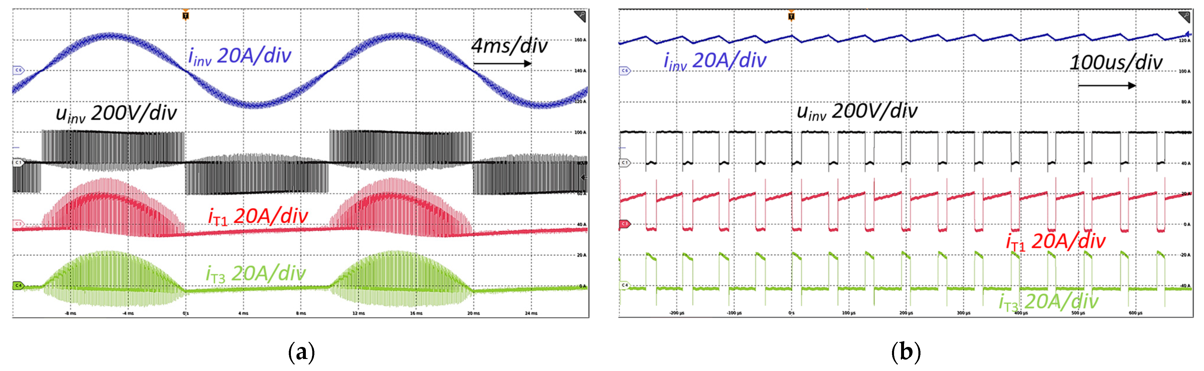
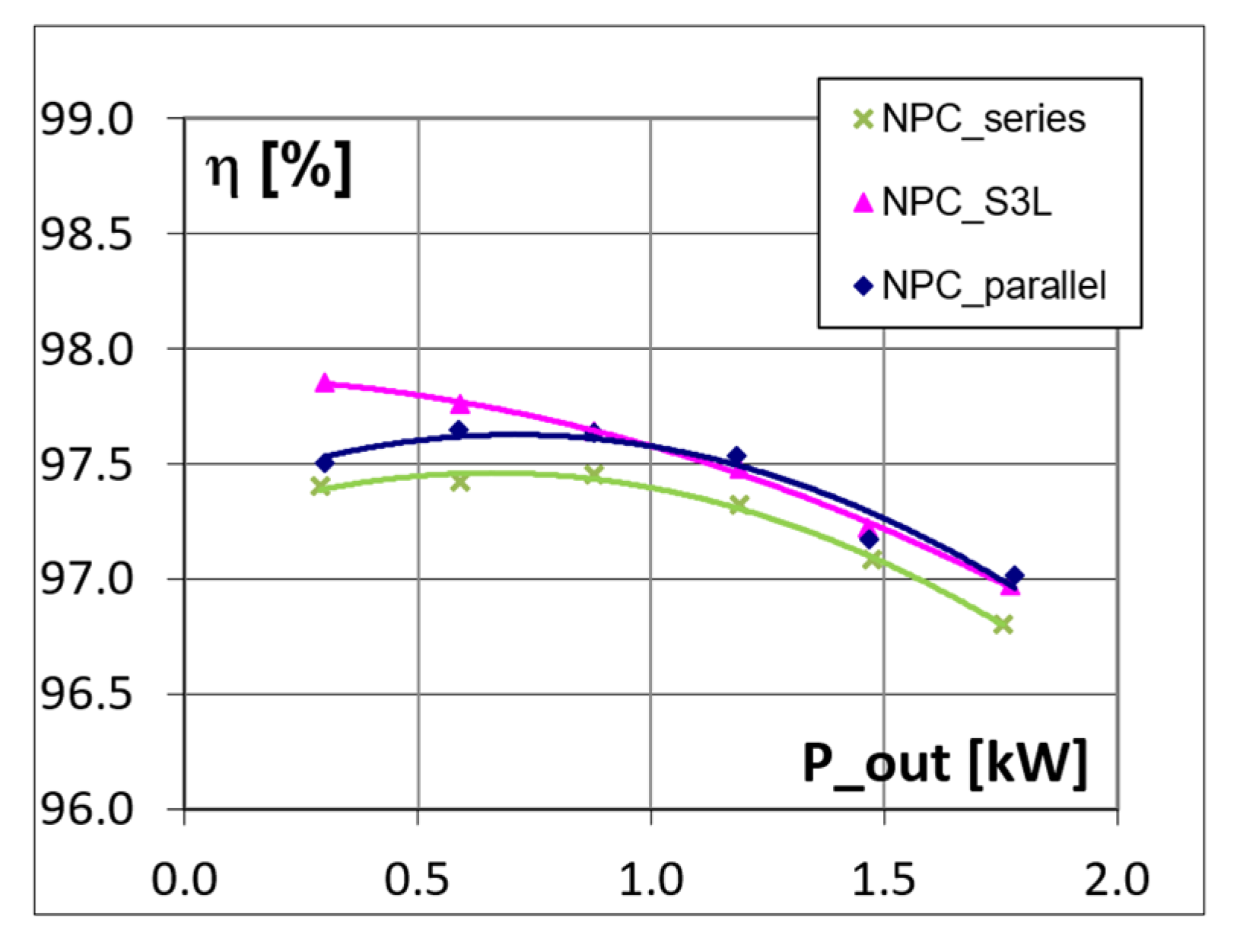
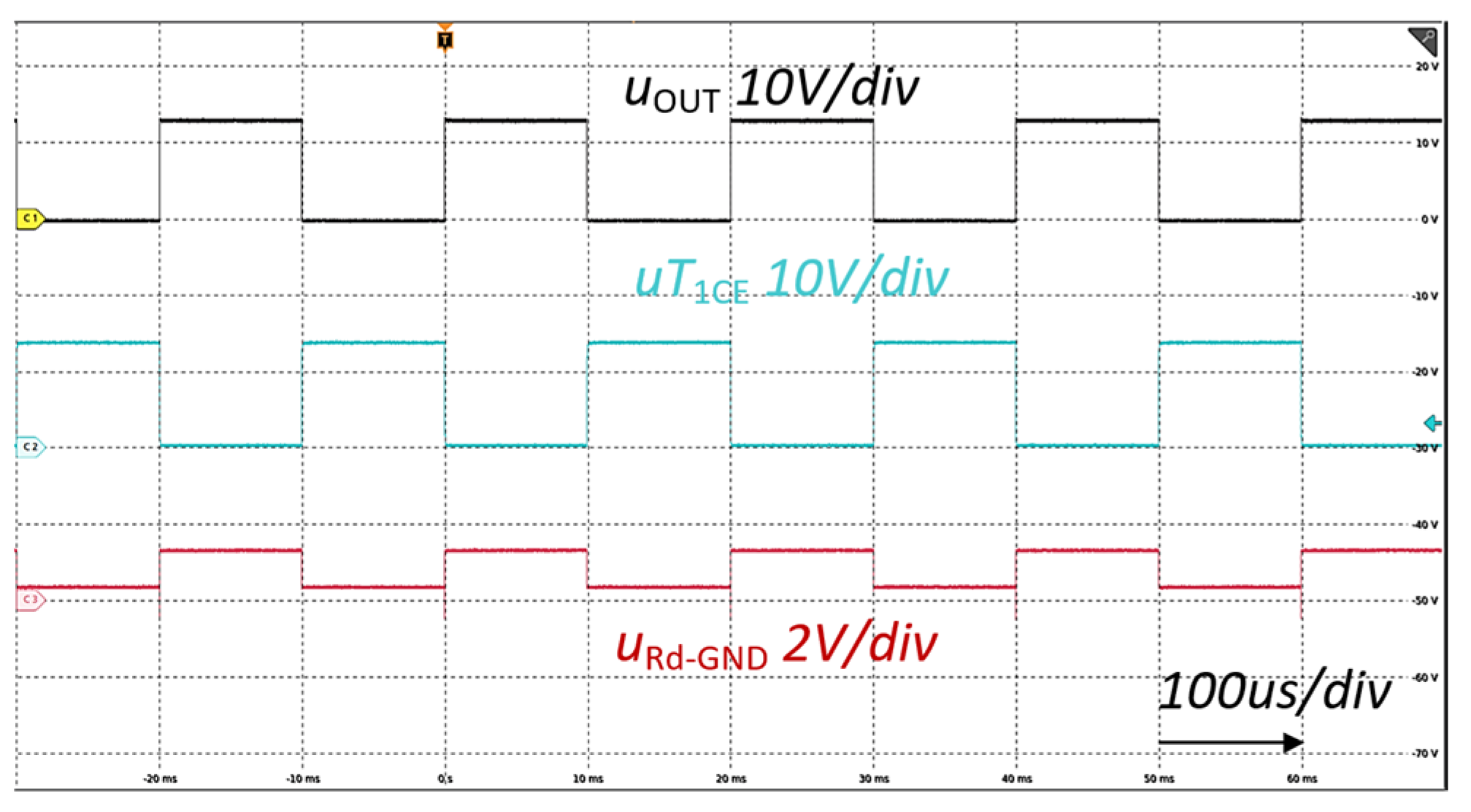
3.2. Result of Measurements

Figure 7 shows a set of voltage and current waveforms of the T-NPC inverter with a horizontal branch consisting of two reverse blocking transistors connected in anti-parallel (from Figure 3). A steady-state case was recorded for a supply voltage Uin = 400 V, a load power approximately Pout ≈ 1.5 kW, and a switching frequency fsw = 15.7 kHz. The waveforms of the inverter output voltage and current as well as the current of transistors T1 and T3 are presented. The obtained results show that such a system operates like a classic T-NPC inverter in the most common topology with two transistors containing body diodes connected anti-series in the horizontal branch. The waveforms shown in Figure 7 are for an active power. For another type of load, the waveforms of inverters with transistors in the horizontal branch connected anti-series or anti-parallel will also be the same.
Figure 8 shows the efficiency results of the three systems presented earlier. The difference in efficiency of the classic T-NPC system compared with the proposed topologies ranges from 0.1% to 0.45%. The largest improvement of approximately 0.5% was visible for the S3L system in the low power range. The number and type of transistors used in the experiments were the same, while the turn-off losses of T1 and T4 have been reduced. For a light load, these losses are relatively large. As the load power increased, their share decreased and remained at 0.15–0.2%. When comparing the efficiency of the system in Figure 3 with a classic T-NPC inverter, the tendency is different than before. The number of semiconductors and conducted losses on them has now been reduced; therefore, the efficiency difference remains at a similar level over the entire load range. The results in this case will always depend to a small extent on the type of transistor used.
Figure 9 shows the measurement results of the driver circuit proposed in Section 2 (Figure 5).
While the driver IC controlled the IGBT transistor in the power circuit (uOUT = 15 V), the auxiliary transistor T1 was switched on with the same signal (Figure 5). This caused the activation of transistor T2 in the DESAT circuit. The power transistor was then switched on and the driver performed voltage drop control on its collector-emitter structure. During this time interval, the current could flow through the IGBT transistor. When the IGBT transistor was not conducting, the signal uOUT = 0 V and transistors T1 and T2 were turned off. The DESAT circuit was disconnected. This solution does not allow current to flow from the emitter potential of the IGBT transistor (e.g., from the power source of the power circuit) through the driver circuit.

4. Discussion

The article presents two concepts to reduce losses in a T-NPC inverter. In each case they gave positive results confirmed by laboratory tests. In case of switching loss reduction, it is necessary to add an LC circuit. This solution is cost-effective in high power systems due to the minimization of relatively high switching losses always occurring during system operation and increasing efficiency. In low-power systems, it may not be cost-effective due to low losses and the possibility of using other types of transistors. In addition, the use of an LC circuit requires a relatively small financial outlay and is a source of little additional loss. However, as shown in the laboratory test, even for a low-power system with IGBT transistors, the use of LC cells increases the efficiency of the system. In the case of limiting the conducted losses, the financial outlay are negligible due to the preservation of the same number of power elements. Similarly, modifying the driver according to the presented solution only requires the investment of two transistors and four low-power resistors. In comparison to existing solutions, the proposed concept is relatively simple and does not require a lot of financial investment. It also does not require the use of high-power current-limiting resistors, which may cause additional power losses and current passing in the protection circuit. The solution proposed in this paper allows RB-IGBT transistors to be used in complete safety. The increase in efficiency in this case will depend on the parameters eliminated and used semiconductors in the horizontal branch. The use of the proposed driver increases the safety of the system.
The proposed gate driver and methods of losses reduction presented In the article can also be applied in many other power electronic systems. Such gate drivers can be used in all applications with RB-IGBTs as well as with all IGBTs. RB-IGBTs with the proposed gate-driver can be applied in a horizontal branch of the T-NPC inverter, current inverters, or matrix converters. The presented resonant cell is dedicated to this topology; however, with appropriate modifications it can affect the minimization of switching losses of transistors in other circuits, such as in buck or boost converters. These issues and also the optimization of the resonance cell are further research directions.

Funding

This research project was partly supported by the program “Excellence initiative—research university” for the AGH University of Science and Technology. Nr ID 4738.

Data Availability Statement

Data sharing not applicable.

Conflicts of Interest

The author declares no conflict of interest. The funders had no role in the design of the study; in the collection, analyses, or interpretation of data; in the writing of the manuscript; or in the decision to publish the results.

References

  1. Rodriguez, J.; Bernet, S.; Steimer, P.K.; Lizama, I.E. A Survey on Neutral-Point-Clamped Inverters. IEEE Trans. Ind. Electron. 2010, 57, 2219–2230. [Google Scholar] [CrossRef]
  2. Nabae, A.; Takahashi, I.; Akagi, H. A new neutral-point-clamped PWM inverter. IEEE Trans. Ind. Appl. 1981, IA–17, 518–523. [Google Scholar] [CrossRef]
  3. Salem, A.; Abido, M.A. T-Type Multilevel Converter Topologies: A Comprehensive Review. Arab. J. Sci. Eng. 2019, 44, 1713–1735. [Google Scholar] [CrossRef]
  4. Wang, Y.; Shi, W.W.; Xie, N.; Wang, C.M. Diode-Free T-type three-level neutral-point-clamped inverter for low-voltage renewable energy system. IEEE Trans. Ind. Electron. 2014, 61, 6168–6174. [Google Scholar] [CrossRef]
  5. Aly, M.; Ahmed, E.M.; Shoyama, M. Modulation Method for Improving Reliability of Multilevel T-Type Inverter in PV Systems. IEEE J. Emerg. Sel. Top. Power Electron. 2020, 8, 1298–1309. [Google Scholar] [CrossRef]
  6. Bhattacharya, S.; Mascarella, D.; Joos, G.; Cyr, J.-M.; Xu, J. A dual three-level T-NPC inverter for high-power traction applications. IEEE J. Emerg. Sel. Top. Power Electron. 2016, 4, 668–678. [Google Scholar] [CrossRef]
  7. Lee, J.-S.; Choi, U.-M.; Lee, K.-B. Comparison of tolerance controls for open-switch fault in a grid-connected T-type rectifier. IEEE Trans. Power Electron. 2015, 30, 5810–5820. [Google Scholar] [CrossRef]
  8. Lee, J.-S.; Lee, K.-B. An open-switch fault detection method and tolerance controls based on SVM in a grid-connected t-type rectifier with unity power factor. IEEE Trans. Ind. Electron. 2014, 61, 7092–7104. [Google Scholar] [CrossRef]
  9. Motto, E.; Donlon, J.; Tabata, M.; Takahashi, H.; Yu, Y.; Majumdar, G. Application characteristics of an experimental RB-IGBT (reverse blocking IGBT) module. In Proceedings of the Conference Record of the 2004 IEEE Industry Applications Conference, 2004. 39th IAS Annual Meeting, Seattle, WA, USA, 3–7 October 2004; Volume 3. [Google Scholar]
  10. Vaidya, M.; Naugarhiya, A.; Verma, S.; Mishra, G.P. Collector Engineered Bidirectional Insulated Gate Bipolar Transistor with Low Loss. IEEE Trans. Electron Dev. 2022, 69, 1604–1607. [Google Scholar] [CrossRef]
  11. Xu, X.; Chen, W.; Wang, F.; Sun, R.; Liu, C.; Xia, Y.; Xin, Y.; Zhou, Q.; Li, Z.; Zhang, B. An Ultralow Loss N-channel RB-IGBT with P-drift Region. In Proceedings of the 2020 32nd International Symposium on Power Semiconductor Devices and ICs (ISPSD), Vienna, Austria, 13–18 September 2020; pp. 455–458. [Google Scholar] [CrossRef]
  12. Kim, U.-J.; Oh, S.-G. New Sub-Module with Reverse Blocking IGBT for DC Fault Ride-Through in MMC-HVDC System. Energies 2021, 14, 1551. [Google Scholar] [CrossRef]
  13. Yang, X.; Xue, Y.; Chen, B.; Mu, Y.; Lin, Z.; Zheng, T.Q.; Igarashi, S. Reverse-blocking modular multilevel converter for battery energy storage systems. J. Mod. Power Syst. Clean Energy 2017, 5, 652–662. [Google Scholar] [CrossRef] [Green Version]
  14. Yang, X.; Xue, Y.; Chen, B.; Lin, Z.; Mu, Y.; Zheng, T.Q.; Igarshi, S. Reverse blocking sub-module based modular multilevel converter with DC fault ride-through capability. In Proceedings of the 2016 IEEE Energy Conversion Congress and Exposition (ECCE), Milwaukee, WI, USA, 18–22 September 2016. [Google Scholar] [CrossRef]
  15. Liu, Y.; Duan, Z.; Chen, Q.; Li, B.; Ban, M.; Li, Z. MMC-modified sub-module structure with double reverse blocking IGBTs. J. Power Electron. 2023, 23, 434–444. [Google Scholar] [CrossRef]
  16. Singh, A.K.; Jeyasankar, E.; Das, P.; Panda, S.K. A matrix-based nonisolated three-phase AC–DC rectifier with large step-down voltage gain. IEEE Trans. Power Electron. 2017, 32, 4796–4811. [Google Scholar] [CrossRef]
  17. Tuan, D.A.; Vu, P.; Lien, N.V. Design and Control of a Three-Phase T-Type Inverter using Reverse-Blocking IGBTs. Eng. Technol. Appl. Sci. Res. 2021, 11, 6614–6619. [Google Scholar] [CrossRef]
  18. di Benedetto, M.; Lidozzi, A.; Solero, L.; Crescimbini, F.; Grbovic, P.J. Reliability and Real-Time Failure Protection of the Three-Phase Five-Level E-Type Converter. IEEE Trans. Ind. Appl. 2020, 56, 6630–6641. [Google Scholar] [CrossRef]
  19. Kolar, J.W.; Ertl, H.; Erhartt, L.L.; Zach, F.C. Analysis of turn-off behavior and switching losses of a 1200 V/50 A zero-voltage or zero-current switched IGBT. In Proceedings of the Conference Record of the 1991 IEEE Industry Applications Society Annual Meeting, Dearborn, MI, USA, 28 September–4 October 1991; Volume 2, pp. 1508–1514. [Google Scholar]
  20. Gekeler, M.W. Soft switching three level inverter with passive snubber circuit (S3L inverter). In Proceedings of the 2011-14th European Conference on Power Electronics and Applications (EPE 2011), Birmingham, UK, 30 August–1 September 2011; pp. 1–10. [Google Scholar]
  21. Gekeler, M.W.; Schreitmueller, S.; Voigt, G. Comparison of the EMC and efficiency characteristics of hard and soft switching three-level inverters. In Proceedings of the International Exhibition and Conference for Power Electronics Intelligent Motion Renewable Energy and Energy Management, PCIM Europe, Nuremberg, Germany, 10–12 May 2016; pp. 1–8. [Google Scholar]
  22. Mondzik, A.; Stala, R.; Penczek, A.; Piróg, S.; Szot, S.; Ryłko, M. Operation Improvement of the Three-Level T-NPC Soft Switching Inverter with Passive Snubber, In Proceedings of the 2020 IEEE 19th International Power Electronics and Motion Control Conference (PEMC), Gliwice, Poland, 25-29 April 2021.
  23. Penczek, A.; Mondzik, A.; Piróg, S.; Twaróg, M.; Stala, R. New Three-Level Soft Turn-off T-type NPC Inverter. In Proceedings of the 21st International Symposium on Power Electronics (Ee), Novi Sad, Serbia, 27–30 October 2021; pp. 1–5. [Google Scholar]
  24. Mazgaj, W.; Szular, Z.; Rozegnal, B. Soft-Switching System with Safe Connections of Capacitors and Inductors in Three-phase Two-level Voltage Source Inverter. IEEE Trans. Power Electron. 2021, 36, 6443–6456. [Google Scholar] [CrossRef]
  25. Grbovic, P.J.; Gruson, F.; Idir, N.; Le Moigne, P. Turn-on Performance of Reverse Blocking IGBT (RB IGBT) and Optimization Using Advanced Gate Driver. IEEE Trans. Power Electron. 2010, 25, 970–980. [Google Scholar] [CrossRef]
  26. Zhou, D.; Sun, K.; Liu, Z.; Huang, L.; Matsuse, K.; Sasagawa, K. A Novel Driving and Protection Circuit for Reverse-Blocking IGBT Used in Matrix Converter. IEEE Trans. Ind. Appl. 2007, 43, 3–13. [Google Scholar] [CrossRef]
  27. Zhou, D.; Liu, Z.; Kong, P.; Sun, K.; Huang, L.; Sasagawa, K. An improved driving and protection circuit for reverse blocking IGBT. In Proceedings of the 2004 IEEE 35th Annual Power Electronics Specialists Conference (IEEE Cat. No.04CH37551), Aachen, Germany, 20–25 June 2004. [Google Scholar] [CrossRef]
  28. Dustert, C.; Volke, A. Implement Gate Drivers for 3-Level NPC2 Modules with Reverse-Blocking IGBTs. Electronic Design, 6 April 2015. [Google Scholar]
  29. Wang, X.; Li, Q.; Wang, S.; Wang, X.; Fu, Y. Design of Driving and protection circuit for Submodule based on cascaded H-bridge STATCOM. IOP Conf. Ser. Mater. Sci. Eng. 2018, 366, 012074. [Google Scholar] [CrossRef] [Green Version]
  30. Mondzik, A.; Penczek, A.; Ryłko, M.; Szot, S.; Szarek, M.; Stala, R. Driver Circuit, Circuit Arrangement Comprising a Driver Circuit, and Inverter Comprising a Circuit Arrangement. U.S. Patent US2018026517-B2, 13 October 2020. [Google Scholar]
  31. Morris, G.K.; Phillips, M.G.; Wei, L.; Lukaszewski, R.A. Operating IGBTs above Rated Junction Temperature Limits: Impacts to Reliability and Electrical Performance. In Proceedings of the 2016 Annual Reliability and Maintainability Symposium (RAMS), Tucson, AZ, USA, 25–28 January 2016; pp. 1–7. [Google Scholar] [CrossRef]
  32. Morozumi, A.; Yamada, K.; Miyasaka, T.; Sumi, S.; Seki, Y. Reliability of Power Cycling for IGBT Power Semiconductor Modules. IEEE Trans. Ind. Appl. 2003, 39, 665–671. [Google Scholar] [CrossRef]
  33. Liu, J.; Zhang, K.; Xiao, H.; Zhu, G.; Mao, X.; Zhang, W.; Chen, F.; Guo, X.; Liu, H. The analysis of IGBT module based on thermal simulation technology. In Proceedings of the 23rd International Conference on Electronic Packaging Technology (ICEPT), Dalian, China, 10–13 August 2022; pp. 1–3. [Google Scholar] [CrossRef]
  34. Chao, F.; Tong, A.; Fei, Q.; Jingyi, Z.; Xuequan, Y. Temperature and stress distribution of IGBT module in DC power cycling test with different switching frequencies. In Proceedings of the 2018 19th International Conference on Electronic Packaging Technology (ICEPT), Shanghai, China, 8–11 August 2018. [Google Scholar] [CrossRef]
  35. Abuelnaga, A.; Narimani, M.; Bahman, A.S. A Review on IGBT Module Failure Modes and Lifetime Testing. IEEE Access 2021, 9, 9643–9663. [Google Scholar] [CrossRef]
Figure 1. T-NPC inverter with resonant cell (S3L).
Energies 16 04642 g001
Figure 2. Stages of operation during turn-on and turn-off of the switch T1 of T-NPC inverter with resonant cell (S3L).
Energies 16 04642 g002
Figure 3. T-NPC inverter with horizontal reverse blocking IGBT transistors connected in anti-parallel.
Energies 16 04642 g003
Figure 4. Functional diagram of the driver: (a) classic; (b) investigated concept.
Energies 16 04642 g004
Figure 5. Practical implementation of the proposed driver.
Energies 16 04642 g005
Figure 6. The laboratory setup of inverter with anti-parallel reverse-blocking transistors in the horizontal branch.
Energies 16 04642 g006
Figure 7. Steady state waveforms of the T-NPC inverter with two anti-parallel connected transistors in the horizontal branch: inverter current iinv (blue) 20 A/div, output voltage of the inverter uinv (black) 200 V/div, current of the transistor T1 iT1 (red) 20 A/div, current of the transistor T3 iT3 (green) 20 A/div; (a) 4 ms/div; (b) 100 us/div.
Energies 16 04642 g007
Figure 8. Efficiency vs. output power of the: classic T-NPC inverter with two anti-series connected transistors in the horizontal branch (NPC_series), inverter with resonant cell from Figure 1 (NPC_S3L), and inverter with two anti-parallel connected transistors in the horizontal branch from Figure 3 (NPC_parallel).
Energies 16 04642 g008
Figure 9. Waveforms of the proposed driver circuit: control signal of the transistor IGBT—uOUT (black) 10 V/div, control signal of the transistor T2uT1CE (cyan) 10 V/div, DESAT signal—voltage across Rd-GND (red) 2 V/div; 100 us/div.
Energies 16 04642 g009
Table 1. Basic parameters of the system.
ComponentParameters
T1, T4IKW40N120
T2, T3 (classic T-NPC and Figure 1)IKW40N120
T2, T3 (Figure 3)IXRH50N120
Passives (Figure 1)C1 = C2 = 22 nF, Lres = 20 uH
Diodes (Figure 1)Dh1, Dh4: C4D20120, Dh2, Dh3: IDP15E60
Input capacitanceCin1 = Cin2 = 4.23 mF
Output filterLf = 150 uH, Cf = 2 × 4, 7 uF
Disclaimer/Publisher’s Note: The statements, opinions and data contained in all publications are solely those of the individual author(s) and contributor(s) and not of MDPI and/or the editor(s). MDPI and/or the editor(s) disclaim responsibility for any injury to people or property resulting from any ideas, methods, instructions or products referred to in the content.

