
A Review on Dry Deposition Techniques: Pathways to Enhanced Perovskite Solar Cells


1
Department of Materials Science and Engineering, Korea University, 145 Anam-ro, Seongbuk-gu, Seoul 02841, Republic of Korea
2
Graduate School of Energy and Environment (KU-KIST Green School), Korea University, 145 Anam-ro, Seongbuk-gu, Seoul 02841, Republic of Korea
*
Author to whom correspondence should be addressed.
†
These authors contributed equally to this work.
Energies 2023, 16(16), 5977; https://doi.org/10.3390/en16165977
Submission received: 7 July 2023
/
Revised: 4 August 2023
/
Accepted: 10 August 2023
/
Published: 14 August 2023
(This article belongs to the Special Issue Advanced Technologies of Solar Cells)
Abstract
:This review discusses the use of evaporation, chemical vapor deposition, and sputtering as the three main dry deposition techniques currently available for fabricating perovskite solar cells. We outline the distinct advantages that each method offers in terms of film quality, control, and scalability. Additionally, recent advancements in process optimization and the integration of dry deposition with other fabrication techniques are highlighted. Thus, this review provides valuable insights into the potential of dry deposition processes to produce high-performance perovskite solar cells and aids researchers and industry professionals in selecting the most suitable technique for the fabrication of efficient and stable devices.
1. Introduction
Perovskite solar cells (PSCs) have gained significant attention in recent years owing to their high power-conversion efficiency and ease of fabrication. A crucial step in the fabrication process is the deposition of perovskite films, which influence device performance directly. Traditional solution-based methods are commonly used to achieve film deposition, such as spin coating and solution casting. However, these methods have limitations, including the need for precise control over solvent evaporation and the potential introduction of impurities.
In response to these challenges, processes employing the deposition of a dry perovskite film offer several advantages over their solution-based counterparts and have emerged as promising production alternatives. This introduction aims to highlight the benefits of dry deposition methods of perovskite film fabrication, focusing on their advantages over solution-based approaches and their utilization in large-area deposition and the manufacturing of perovskite/silicon tandem solar cells. One significant advantage of dry techniques is that they provide an enhanced control over film morphology, thickness, and uniformity [1,2,3,4,5,6]. Techniques such as physical (PVD) or chemical vapor deposition (CVD) enable the precise manipulation of deposition parameters, resulting in improved film quality and reproducibility [7,8,9,10,11,12,13,14]. Another advantage of dry processes is that they eliminate all solvent-related issues encountered in solution-based methods. Specifically, they do not require the use of organic solvents, which mitigates associated challenges such as solvent retention, nonuniform drying, and solvent compatibility with other device components. This contributes to the enhanced stability and long-term performance of PSCs.
Dry processes furthermore excel in scalability when it comes to large-area depositions [15,16,17,18,19,20], rendering them suitable for fabricating perovskite films on substrates of a commercial size. This is crucial for the industrial production of perovskite solar modules and enables the manufacturing of cost-effective and efficient photovoltaic devices. Moreover, dry deposition techniques exhibit excellent compatibility with perovskite/silicon tandem solar cells [21,22,23]. When depositing conformal perovskite films on textured silicon surfaces, the dry processes ensure efficient light harvesting and improve device performance in tandem solar cell configurations. This compatibility creates opportunities for achieving higher power-conversion efficiencies by leveraging the advantages of both perovskite and silicon technologies.
In summary, the key benefits of dry processes over traditional solution-based methods for perovskite film fabrication are an enhanced control over film properties, the reduction in solvent-related issues, scalability to large areas, and compatibility with perovskite/silicon tandem solar cells. Leveraging these advantages can further advance the development of high-performance PSCs and promote their commercialization and integration into the renewable energy landscape (Figure 1). Previous review papers on dry-process-related perovskite solar cells have focused on specific processes [24,25,26,27]. In this review, we have collated literature including various and recent research trends on perovskite film fabrication through diverse dry processes. We have investigated the advantages and limitations of each process. Notably, the efficiency of PSCs fabricated via dry processes is currently approaching the efficiency record attained by solution-based counterparts (Figure 2 and Table 1).
2. Dry Processes for Perovskite Film Deposition
2.1. Evaporation
Thermal evaporation is a widely used deposition method for thin-film fabrication. It offers several advantages, including simplicity, high deposition rates, and the capability to deposit various materials, such as metals, organic compounds, and inorganic materials. For organic-inorganic perovskite evaporation, the ratio of the source material evaporation rate plays a crucial role in determining the stoichiometry of the deposited film and efficiency of solar cells. The ratio of the evaporation rate is influenced by factors such as the vacuum chamber pressure, crucible heating power, and quantity and distribution of evaporation materials in the crucibles. However, difficulties arise when attempting to control the deposition rate of organic halide materials at high vapor pressures. Various studies have been conducted to address this issue and fabricate high-efficiency PSCs, primarily focusing on one of two methods: single-step evaporation, in which multiple source materials are deposited simultaneously [29,30,31,32,33,34,35,36,37,38,39,70,71,72,73,74,75,76,77,78,79], and multiple-step evaporation, in which multiple depositions are performed sequentially [28,40,41,42,43,44,45,46,47,80,81,82].
2.1.1. Single-Step Evaporation
The deposition of PSCs through single-step evaporation has primarily been investigated using a co-evaporation method, in which organic and lead halides are simultaneously deposited. In 2013, Liu et al. successfully deposited a planar perovskite film by co-evaporating methylammonium iodide (MAI) and lead chloride (PbCl2) [29]. By optimizing the deposition conditions, uniform, flat perovskite films could be obtained, resulting in the fabrication of PSCs with a simplified planar structure that achieved a power conversion efficiency (PCE) of 15% without having to rely on a nanostructure. In 2014, Malinkiewicz et al. studied the properties of PSC devices when varying the perovskite film thickness [30]. They proposed that controlling the evaporation rate of MAI is the main challenge to deposit high-quality perovskite films. The calibration process for MAI turned out to be inaccurate for thickness measurement using a profilometer due to its soft and volatile nature. To address the challenge of accurately measuring MAI thickness, they adjusted the evaporation temperature of PbI2 while maintaining the temperature of MAI in a crucible. By optimizing the film thickness and employing an organic charge transport layer (CTL), they successfully fabricated metal-oxide-free PSCs with a PCE of 15%. In 2020, Kim et al. established the growth kinetics of PbI2 and MAI during the evaporation process for MAPbI3 deposition. By investigating the rates under different evaporation conditions, they developed a simple model to explain the growth kinetics. The growth rate of MAI, extracted from the quartz crystal microbalances, was determined by establishing kinetic equations that describe the MAI adsorption as a surface-dependent and diffusion driven process. Furthermore, by considering the surface-dependent adsorption of MAI and incorporating geometric factors, they demonstrate the ease of estimating the composition of MAPbI3 films. They fabricated four different perovskite films with a fixed PbI2 rate of 1 Å·s−1 and varying MAI rates. It was found that when the thicknesses of PbI2 and MAI are 440 nm and 183 nm, respectively, the atomic ratio of PbI2:MAI approaches 1:1. The authors concluded by showing that with this control method, they fabricated vacuum-processed perovskite solar cells with an average PCE exceeding 18% [48]. Chiang et al. aimed to improve long-term stability by depositing a methylammonium (MA)-free perovskite film with a composition of FA0.7Cs0.3Pb(I0.9Br0.1)3, excluding the volatile MA component, as shown in Figure 3a,b [33]. In 2018, Gil-Escrig et al. specifically focused on incorporating excess PbI2, resulting in the fabrication of p-i-n solar cells with a PCE of 18.2%. Furthermore, the authors investigated the influence of substrate type and temperature on surface chemistry, providing valuable insights on how the composition of perovskite films can be optimized via co-evaporation. Subsequently, they used four co-evaporation sources—MAI, cesium bromide (CsBr), formamidinium iodide (FAI), and lead iodide (PbI2)—to deposit a triple-cation, double-halide perovskite film with a composition of Cs0.5FA0.4MA0.1Pb(I0.83Br0.17)3, as illustrated in Figure 3c,d [32]. Further, they suppressed hysteresis according to the scan direction of the PSCs by partially substituting the cation with Cs and inhibiting the residual δ-phase. By measuring cross-contamination, the deposition rate of each source material could be accurately regulated, which in turn enabled control over the composition and morphology of the resultant perovskite film. As a result, fully vacuum-deposited PSCs with a PCE of 16% could be fabricated by depositing a doped CTL.
In 2021, Ross et al. improved the phase stability of FAPbI3 at room temperature by adding excess FAI [35]. They reported enhanced device performance with the ability to maintain 100% of the initial efficiency under operating conditions for 1000 h, along with a PCE of 20.4% (Figure 3f). Notably, they achieved a significant milestone by fabricating monolithic, fully textured silicon/perovskite tandem solar cells with a PCE of 24.6% by fully covering the pyramid texture using co-evaporation (Figure 3e). Subsequently, Li et al. used interfacial optimization, surface treatment, and light management to achieve PCEs of 20.28% and 18.13% with active areas of 0.16 cm2 and 21 cm2, respectively [34]. They demonstrated that surface treatment with potassium acetate can immobilize excess halide and Pb-I antisite defects, thereby improving conductivity at grain boundaries. A Nyquist plot of impedance measurements verified that this surface treatment suppressed charge recombination in the PSCs.
Zhang et al. introduced a co-evaporation method involving cesium iodide (CsI), CsBr, and phenylethylammonium iodide (PEAI) to incorporate PEAI into CsPbI3 films, which is commonly used for doping and passivating materials for perovskite in solution-based processes [37]. This simultaneous deposition enabled the fabrication of PEAI-doped CsPbI3 films. Furthermore, it was confirmed that the orientation along the (0 0 l) plane was enhanced through PEAI doping, which improved charge transport characteristics and suppressed the (1 1 0) and (2 2 0) diffraction peaks in X-ray diffraction (XRD) patterns. This method reduced the trap density and thereby achieved an improved stability in the γ-CsPbI3 phase and a PCE of 15% (Figure 3g,h).
On the other hand, researchers have explored single-source evaporation, another approach to single-step evaporation. In 2016, Fan et al. successfully deposited reproducible perovskite films with high crystallinity and full surface coverage through the single-source evaporation of as-prepared MAPbI3 crystals (Figure 3i–k) [39]. High-quality MAPbI3 crystals with few impurities were obtained by maintaining the precursor solutions. The advantage of single-source deposition is that it does not require post-annealing to evaporate the solvent or crystallize the perovskite. This is because the MAPbI3 vapor is directly transported to the substrate without undergoing any chemical reactions during the deposition process. This method achieved a PCE of 10.9% by overcoming the challenges associated with controlling the deposition process during dual-source evaporation. Subsequently, Li et al. developed an evaporation source by compressing a mixture of CsBr and lead bromide (PbBr2) powders into tablets and utilized single-source evaporation to deposit CsPbBr3 films. By adjusting the CsBr to PbBr2 ratio in the precursor, they obtained high-quality, uniform films with a large grain size and PCE of 8.65% [78]. Furthermore, in 2019, Peng et al. utilized single-step evaporation with MAPbI3 powder to deposit a perovskite film that was subsequently exposed to solvent annealing, which involve heating in a sealed container under a solvent-vapor atmosphere. This process allows solvent vapor to penetrate grain boundaries, partially dissolving and recrystallizing the perovskite. Consequently, the solvent-annealed film exhibited larger grains and accelerated charge extraction processes, which increased the PCE from 2.64% to 9.92%.
2.1.2. Multi-Step Evaporation
Although the co-evaporation technique has shown promising results, its use in the fabrication of a perovskite film is complicated because of the small molecular weight of MAI, which results in the random diffusion of molecules within the vacuum chamber. Consequently, it is challenging to monitor and control the deposition rate of MAPbI3 with quartz sensors. To address this challenge, a sequential evaporation method was proposed, in which source materials are sequentially deposited, layer by layer, and subsequently crystallized.
In 2014, Chen et al. fabricated a MAPbI3 film through the sequential evaporation of PbCl2 and MAI and subsequent heating of the substrate. They proposed that the small molecular weight of MAI leads to random diffusion of molecules within the chamber, making it challenging to accurately monitor and control the MAI deposition rate using quartz microbalance sensors. Therefore, the temperature of MAI crucible was maintained at 85 °C during the evaporation process, while the substrate temperature was varied from 60 °C to 85 °C, showing increase in the reaction penetration depth. During this process, the as-deposited PbCl2 is converted into perovskite by in situ MAI deposition, with its electrical and optical properties differing depending on the substrate temperature. The authors reported a PCE of 14% with this method, which offered advantages such as a larger grain size and improved control over the process (Figure 4a,b) [40]. In 2015, Yang et al. also fabricated a MAPbI3 film, using multiple layer-by-layer evaporation of PbCl2 and MAI. Subsequently, the PbCl2 and MAI were confirmed to exist as individual layers, and after annealing, the MAI was intercalated into PbCl2 to form perovskite. Thus, they could optimize the thickness and surface morphology of perovskite films by controlling the number of layers. A PCE of 16% was achieved with a large active area of 1 cm2 [41].
In 2019, Kam et al. fabricated a mixed perovskite film composed of MA0.56FA0.44PbI2.67Br0.33 using the sequential evaporation of mixed organic (FAI + MAI) and lead halides (PbI2 + PbBr2), as shown in Figure 4c,d [43]. They proposed that the drawback of using multiple quartz crystal microbalance to monitor each precursor during co-evaporation could be solved by sequential evaporation of each precursor. The mixed organic halide and mixed lead halide materials were able to be evaporated together in one crucible due to their similar boiling points. Each of their evaporation rates was maintained at 1.5 to 2.0 Å s−1 to obtain the thickness of 120 nm and 280 nm of lead halide and organic halide. The composition of the final film was controlled by adjusting the ratio of the components in the precursor. Furthermore, they obtained a PCE of 15.1% by fabricating all-vacuum-processed PSCs using RF-sputtered SnO2 as the ETL and thermally evaporated CuPc as the HTL. To further improve efficiency, sequential step deposition has been investigated, a process that combines evaporation and various deposition techniques. In 2021, Feng et al. fabricated a FAxCs1-xPbI3 perovskite film via the sequential evaporation of CsI, FAI, and PbI2 sources, followed by in-vacuum annealing [44]. Through optimization of the in-vacuum annealing temperature, PbI2 formation could be suppressed to enhance the perovskite crystallinity, as verified via XRD. During sequential evaporation, FAI only reacts with the uppermost surface of pre-deposited PbI2 and fails to diffuse, undergoing a discontinuous reaction throughout the layer. Therefore, the authors applied in-vacuum annealing, which promoted the diffusion of the FAI and CsI sources into the film bulk and resulted in the formation of a large-grain perovskite film with a PCE of 21.32%.
In 2022, Li et al. deposited a Cs0.05FA0.95PbI3-xClx film using a combination of co-evaporation of PbCl2, PbI2, and CsI, followed by the sequential evaporation of organic FAI (Figure 4e) [45]. They demonstrated that the incorporation of chlorine (from PbCl2) into the perovskite increased its crystallinity and induced a stronger preferred orientation, as confirmed via grazing incidence wide-angle X-ray scattering and XRD characterization (Figure 4f). Consequently, they achieved high PCEs of 24.42% and 19.87%, respectively, with an aperture area of 14.4 cm2 (Figure 4g).
In 2023, Tan et al. fabricated a CsxFA1-xPbIyBr3-y perovskite film by depositing PbI2 and CsI using co-evaporation followed by the deposition of organic ammonium halide through a solution-based process [28]. When reacting with organic ammonium halide in the PbI2 film created using a solution-based approach, various intermediates were formed. However, when applied to evaporated PbI2, rapid diffusion and intercalation suppressed the phase and formed a pure-phase perovskite film. Using this method, the authors reported a large grain size, high reproducibility, a PCE of 24.3%, and demonstrated stability, with 90% of the initial efficiency maintained after 1000 h of 1-sun operation.
In 2017, Zhu et al. fabricated a pinhole-free Cs-substituted MA0.77Cs0.23PbI3 perovskite film via a direct contact and intercalation process [46]. They deposited PbCl2 and CsCl through co-evaporation and then annealed them onto MAI powder to incorporate MAI into the film. The trap state density was reduced and the carrier lifetime was increased, as confirmed with photoluminescence (PL) and time-resolved PL (TRPL) measurements. A PCE of 20.13% and excellent stability were reported, with only a 2% decrease in efficiency after one-year storage in the dark. These results can be attributed to strain relaxation resulting from a decrease in the lattice parameter due to the substitution of Cs, which has a relatively small ionic radius.
In 2018, Luo et al. fabricated a Cs0.24FA0.76PbI3-yBry film using a vapor-solid reaction. This method involves the sequential thermal evaporation of CsBr and PbI2 followed by annealing in a tube furnace, where the deposited film and FAI/formamidinium chloride (FACl) films face each other, resulting in transformation of the CsBr/PbI2 composite [47]. Of particular note, the authors introduced FACl to accelerate the growth rate and enhance phase stability, which was confirmed by the removal of the PbI2 peak and an increase in the α-phase intensity observed in the XRD pattern. The authors reported a PCE of 17.29% with an area of 0.09 cm2 and 12.24% with a PSC module of 8 × 8 cm2.
2.2. Chemical Vapor Deposition
CVD offers several advantages over conventional perovskite deposition methods. First, it enables precise control over the composition and stoichiometry of perovskite films through the accurate delivery of precursor gases. This allows the formation of uniform, well-defined crystal structures, which are crucial for optimizing the optoelectronic properties of perovskite materials. Second, CVD facilitates the deposition of perovskite films on a wide range of substrates, including flexible and nonplanar surfaces. This versatility opens new possibilities for the integration of PSCs into various device architectures and applications. Furthermore, CVD offers the potential for large-scale production of perovskite films through its excellent reproducibility and scalability. Such an ability to deposit perovskite films in a continuous and controlled manner is advantageous for industrial-scale manufacturing.
In this section, we present a comprehensive investigation of perovskite film deposition using double-zone [7,49,50,51,52,53,54,55,56,57,83,84,85,86,87,88] and single-zone CVD methods [58,59,60,61,62,63,64,65]. We explore growth parameters and optimization strategies to achieve high-quality films with improved crystallinity, uniformity, and enhanced optoelectronic properties. In addition, we discuss the potential application of CVD-deposited perovskite films in high-performance solar-cell devices.
2.2.1. Double-Zone Furnace with Carrier Gas Flow
In 2014, Leyden et al. proposed a novel approach for forming MAPbI3 perovskite films by spin-coating PbCl2 precursor films onto MAI vapor using a double-zone CVD process (Figure 5a) [7]. Although previous studies have explored perovskite film formation using CVD, this study marked the pioneering application of this technique to solar cells. The authors compared solar cell efficiencies by varying the thickness of the precursor film, PbCl2, and the annealing atmosphere. The substrate temperature was set at 130 °C while the source temperature was increased to 185 °C. Notably, with a result of 11.8% efficiency, the study reported the highest solar cell efficiency for a perovskite film with an approximate thickness of 300 nm obtained through annealing under ambient conditions. Furthermore, the stability of the solar cell device in a nitrogen gas atmosphere was confirmed for over 1100 h. The authors employed a similar approach to form FAPbI3 perovskite films using FAI as the source material [50], achieving a device efficiency of 14.2% with stability for over 155 days in an inert environment. Moreover, in 2016, they reported an efficiency of 15.6% using an evaporated PbI2/PbCl2 precursor and CVD (Figure 5b) [49]. Notably, they extended their research beyond single cells with small areas to fabricate modules on a 25 cm2 substrate that consisted of five interconnected single cells. This module exhibited an efficiency of 9.6% and active area of 8.8 cm2 (Figure 5c).
In 2015, Tavakoli et al. reported a one-step method for the formation of perovskite films using double-zone CVD through the simultaneous deposition of PbX2 (X = I or Cl) and MAI powder sources [83]. This approach offers commercial advantages over sequential deposition because it simplifies the process. Moreover, it minimizes the issues that can arise at the substrate interface owing to incomplete conversion by avoiding perovskite transformation from the precursor film. As such, they successfully fabricated perovskite films with large grains, uniform surface coverage, and reduced pinhole formation, achieving a solar cell efficiency of 11.1%.
In 2016, Yin et al. proposed a method for the formation of perovskite films by reacting MAI vapor with a PbI2 substrate using a quartz tube connected to a heat gun generating hot air flow [51]. This process has the advantage of not requiring a vacuum, making it suitable for experimental design at the laboratory scale. The authors reported that the humidity inside the tube was approximately 10%, while the external relative humidity was approximately 40%. Importantly, they artificially formed a mesoporous PbI2 film which enhanced reactivity with MAI vapor and minimized the formation of residual layers or defects at the interface. Using this method, they achieved a solar cell efficiency of 18.9%, thus approaching the world record for efficiency in PSCs fabricated using solution-based processes. These highly promising results demonstrate significant advances in this field.
To improve the properties of perovskite films deposited via double-zone CVD, Tong et al. recently proposed a method for enhancing the characteristics of SnO2 surfaces using potassium sulfamate (H2KNO3S) (Figure 5d,e) [57]. They reported solar cell efficiencies of 21.98% (0.09 cm2), 16.16% (22.4 cm2), and 12.12% (91.8 cm2). Additionally, they demonstrated the long-term stability of small-area devices without encapsulation, maintaining a performance of 80% of the initial efficiency for more than 4000 h under solar cell operating conditions (AM1.5G, nitrogen atmosphere, 5% RH, room temperature).
2.2.2. Single-Zone Furnace
Several studies have described the fabrication of perovskite films using single-zone quartz tubes. Compared to the double-zone CVD method, the single-zone CVD method has the advantage of placing the precursor film and source materials in close proximity. This reduces the influence of the carrier gas and enables a more uniform conversion into perovskite.
In 2016, Shen et al. employed a low-pressure hybrid CVD method where spin-coated PbI2 films and MAI powder are placed on a graphite boat (Figure 6a) [58]. Subsequently, the samples were heat treated in a tube furnace to produce perovskite films. They reported a device efficiency of 15.37% after solar cell fabrication. Additionally, they observed the changes in perovskite film characteristics based on the concentration of the PbI2 precursor solution used for spin coating, highlighting the importance of the precursor film in the sequential conversion process. Li et al. reported a method for fabricating low-dimensional 2D or 2D/3D mixed perovskite films using a low-pressure vapor-assisted solution deposition method [60]. Particularly, they incorporated PEAI into a spin-coated precursor film and reacted it with MAI vapor in a quartz tube to form highly crystalline perovskite films, achieving a solar cell efficiency of 19.1%. This study highlights the potential of incorporating 2D materials to improve film and device characteristics in the sequential deposition of perovskite films. Furthermore, Li et al. employed an evaporation method to deposit PbI2 films instead of using a solution-based approach [63]. These films were then reacted with PEAI/MAI vapor in a low-pressure reaction device to form perovskites. In contrast to previous studies in which 2D materials were incorporated into precursor films, here the authors introduced 2D materials during the perovskite transformation process. The characteristics of the films and devices were investigated based on the chemical mass ratio of PEAI/MAI present during the perovskite conversion process, revealing that a higher PEAI ratio improved moisture stability. However, the highest device efficiency of 18.08% was achieved using 10% PEAI, demonstrating the importance of determining an optimal amount of 2D material for incorporation to enhance both stability and device performance.
More reports exist on the deposition of precursor films through evaporation (rather than solution processes) and their conversion into perovskite films using CVD, providing insights into the directional deposition of large-area perovskite films. Tong et al. utilized stack-sequence CVD, in which CsBr/PbBr2 precursor films are evaporated and subsequently annealed at 140 °C with FAI powder in a furnace to form perovskite films [61]. The presence of Cs and Br played a crucial role in controlling the lattice parameters of the FA-containing perovskite, suppressing the formation of the yellow phase (delta: non-perovskite phase) and maintaining the black phase (alpha: perovskite phase) at room temperature. Furthermore, the addition of Cs effectively inhibited pinholes on the film surface, resulting in superior coverage during the perovskite transformation process. With this technique, they achieved a PCE of 18.22% by fabricating solar cells with a FTO/c-TiO2/Cs0.15FA0.85PbI2.85Br0.15/spiro-MeOTAD/Au structure. Of particular note, under 40% RH conditions without encapsulation, the Cs-containing perovskite films exhibited relatively high moisture stability compared with their Cs-free counterparts, as confirmed by evaluation of the device performance over a testing period of 1440 h.
In 2021, Luo et al. employed a three-step multistage atmosphere-assisted (MSA) process [64]. First, thin RbCs-PbI2 films were deposited through evaporation. In the second step, these films were reacted with FACl vapor to form a colorless intermediate phase, RbCs-FA2Pb(BryCl1-y)4, with a 2D orientation. In the third step, the intermediate phase further reacted with FAI to fabricate a perovskite film. The direct reaction between a precursor film and FAI may not be complete owing to the low migration activity of FAI. To overcome this challenge, the two-step approach described above involved the application of FACl to incorporate relatively small Cl− ions, whereby perovskite structures are rapidly formed as an intermediate phase. Subsequently, reactivity with FAI enables halide ion exchange, facilitating the formation of a complete perovskite film. This strategy is effective in achieving efficient and thorough perovskite formation while minimizing residual layers, resulting in a high PL intensity (Figure 6b). Using this method, the authors fabricated a solar cell with an FTO/SnOx/perovskite/Spiro-OMeTAD/Au structure and a PCE of 19.59%. Figure 6c illustrates the formation of a uniform perovskite film on a 64 cm2 substrate during this process. Similarly, Niu et al. fabricated perovskite films by reacting evaporated CsBr/PbI2 precursor films with FAI/FACl vapors [65]. However, during the perovskite conversion process, FACl exhibits fast diffusion in the solid phase, favoring complete perovskite transformation. Notably, this results in a significantly reduced Br concentration, posing challenges in bandgap engineering and leading to a decrease in the open-circuit voltage (Voc) during device fabrication. To achieve the desired composition with an appropriate Br/I ratio in the perovskite film, alkali metal iodide compounds (NaI, KI, and RbI) were used during precursor film deposition, enabling control over the concentration of halogen species in the vapor-solid reaction. Rb doping particularly improved the crystallinity and grain size of the perovskite films (Figure 6d,e). Consistent with previous studies, Na+, K+, and Rb+ cations effectively interacted with Br− anions, inhibiting their mobility. Density functional theory calculations confirmed the formation energies of the respective cations in the presence of Br− anions, with Na, K, and Rb exhibiting energies of −0.86, −1.29, and −1.35 eV, respectively. Additionally, the addition of Rb yielded the lowest density defect in space-charge-limited-current measurements. Figure 6f depicts solar cells with a FTO/SnOx/Rb-Cs0.14FA0.86Pb(BrxI1−x)3/spiro-OMeTAD/Au architecture, which had a high Voc of 1.13 V and a PCE of 19.6%.
2.3. Sputtering
In this section, we explore the advantages of perovskite deposition through sputtering and investigate the influence of the sputtering parameters on film quality and device performance [22,23,66,67,68,69,89,90]. We present a systematic study on the optimization of sputtering conditions aiming to produce high-performance PSCs. By harnessing the benefits of sputtering, it is possible to advance the use of perovskite photovoltaics and pave the way for their widespread implementation in renewable energy systems.
The sputtering process offers several advantages over conventional methods of perovskite deposition. First, it allows a precise control over film thickness and composition through the manipulation of sputtering parameters, such as direct-current (DC) or radio-frequency (RF) power, working pressure, and target material composition. This enables the fabrication of uniform and well-defined perovskite films with tailored properties such as an optimal bandgap and crystallinity. Second, sputtering can be performed at relatively low temperatures, which is advantageous because of its compatibility with temperature-sensitive substrates. This feature expands the range of possible substrates for perovskite deposition to include flexible and nonplanar surfaces, thereby enabling the integration of PSCs into diverse device architectures. Furthermore, sputtering offers excellent film coverage and conformity even on textured or rough substrates. This ensures efficient light absorption and charge transport within the perovskite layer, leading to enhanced device performance. Moreover, sputtering is a scalable deposition technique suitable for large-area production, and its cost-effectiveness is further emphasized by its lower consumption of source material compared to other methods. The ability to deposit perovskite films using high-throughput sputtering systems facilitates the translation of laboratory-scale research into industrial-scale manufacturing, rendering this method a promising candidate for commercial application.
In 2017, Zhang et al. proposed a method for the formation of perovskites by depositing PbO precursor films using DC-reactive magnetron sputtering with a metallic lead target in an Ar/O2 mixed-gas atmosphere, followed by immersion in an MAI/IPA solution [66]. Generally, PbO films undergo a volume expansion of approximately 5–6 times during conversion into MAPbI3. However, in this study, PbO films were deposited on a loosely structured nanocrystalline layer of rutile titania, resulting in a loose morphology and a relatively small, 3–4-fold volume expansion. In particular, the interface between the perovskite and the nanocrystalline rutile titania (NRT) layer (into which the perovskite was naturally absorbed) was effective at extracting electrons. In line with this, researchers have fabricated devices with FTO/NRT/CH3NH3PbI3/Spiro-MeOTAD/Au structures, for which a solar cell efficiency of 14.1% was reported.
In 2020, Hwang et al. proposed a method for depositing PbO films using a RF magnetron sputtering system with the subsequent formation of perovskite films via CVD using MAI vapor [67]. Their study demonstrated the potential for uniform perovskite film deposition on a 100 cm2 textured silicon substrate, highlighting the conformal growth of perovskite films along the pyramid-shaped features of the silicon surface. However, residual layers remained at the interface owing to the volumetric expansion of the PbO film, necessitating additional post-treatment processing to address this issue. They reported the fabrication of FTO/TiO2/MAPbI3/Spiro-MeOTAD/Au devices that achieved a solar cell efficiency of 10.2%. Subsequently, within the same research group, Lee et al. fabricated perovskite films via a direct contact reaction between sputtered PbO films and MAI powder [22]. They analyzed the stress that could occur on patterned V-groove textured silicon substrates using-PL 2D and-LBIC 3D mapping techniques and observed a lower intensity in the tip and valley regions compared to the flat zone. Therefore, it is important to increase the porosity of the precursor film during the two-step perovskite conversion process on textured Si substrates to minimize volumetric expansion and alleviate stress. Overall, these studies emphasized the significance of techniques aimed at reducing stress.
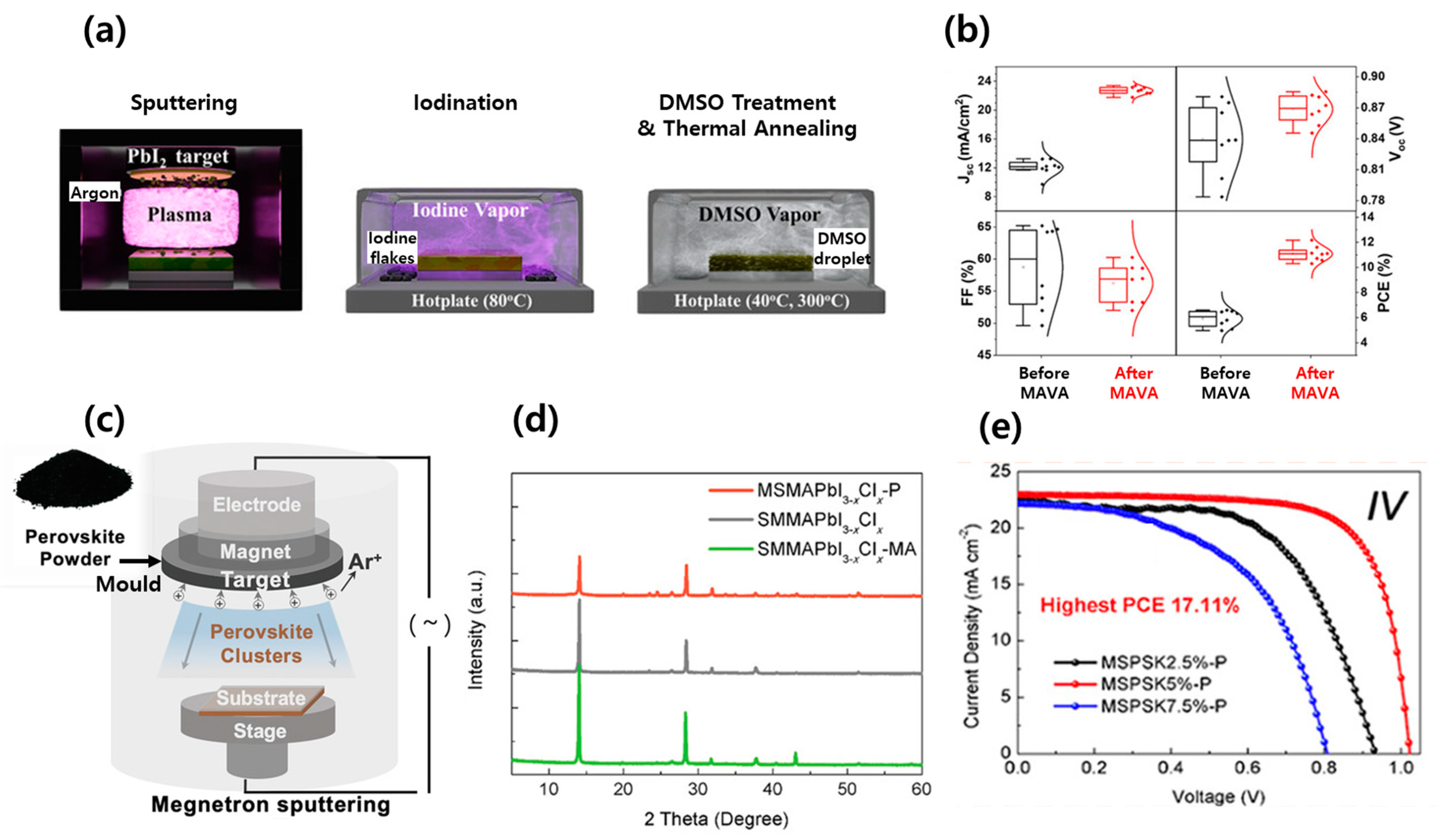
In 2023, Hwang et al. reported post-treatment processes for sputtered PbI2 films to enhance the characteristics of both films (Figure 7a) [23]. Specifically, they proposed methods—such as iodination and thermal and DMSO solvent annealing—that can improve the stoichiometry, crystallinity, and porosity of the precursor films. Additionally, they achieved recrystallization of the perovskite films through methylamine vapor annealing, leading to an improved carrier lifetime. Consequently, they successfully fabricated solar cells with an efficiency of 12.2% (Figure 7b). These findings highlight the importance of post-treatment techniques for optimizing perovskite film properties to enhance device performance.
In 2021, Gao et al. fabricated a single perovskite target for depositing a light-absorbing layer [90]. Figure 7c focuses on this single-step process, which eliminates the need for precursor conversion, simplifies the fabrication process, and reduces the impact of interfacial issues caused by volume expansion. By depositing MAPbI3 perovskite films using a single-step sputtering process, the authors achieved a PCE of 4.64% in solar cell devices. To improve the perovskite layer characteristics, they also investigated the reducing effects of MAI gas, MA gas, and Cl doping treatments on defects within the film, which led to an increased carrier lifetime and crystallinity (Figure 7d). Ultimately, PCE values exceeding 15% were obtained. Using a similar method in 2022, the same research group achieved a PCE of 17.1% by controlling the materials and structure of PSCs (Figure 7e) [68].
3. Conclusions
Based on a thorough examination of various existing deposition methods—including evaporation, CVD, and sputtering—it is evident that each technique presents unique advantages and challenges in the production of perovskite films for solar cell applications:
Evaporation offers an exceptional level of precision in terms of film thickness and uniformity, leading to the fabrication of high-quality perovskite layers. Moreover, the inherent vacuum process minimizes contamination risks. However, the high temperature required for evaporation can limit the compatibility of this technique with temperature-sensitive substrates. Moreover, scalability to large-scale manufacturing remains a challenge owing to the complexity and cost of maintaining high-vacuum environments.
Chemical vapor deposition (CVD), on the other hand, offers a viable alternative that excels in depositing uniform and large-area films under controlled atmospheric conditions. This process is effective for the incorporation of dopants, which enables the tuning of film properties such as bandgap and crystallinity. The major challenges of CVD include film stoichiometry control and the need for high deposition temperatures, which can be detrimental to certain substrates.
Sputtering provides a flexible solution. This technique allows an accurate control over film thickness and composition at relatively low temperatures, making it highly compatible with a broad range of substrates. Further, its scalability renders it suitable for industrial-scale production. However, complex sputtering parameters require meticulous optimization to obtain the desired film characteristics.
In summary, although each deposition technique has its strengths and limitations, the optimal method for perovskite film deposition largely depends on the specific application requirements, such as the type of substrate, desired film properties, and production scale. Considering the techniques used in the production of other thin-film solar cells (e.g., CIGS cells), it can also be advantageous to investigate the direct use of gases for controlling the composition of perovskite materials, rather than solely depending on the vapor derived from powders. Additionally, dry processing might not be suitable for roll-to-roll processes, and the high cost of vacuum equipment setup and substantial source consumption could pose constraints for commercialization rather than solution-based process. Moreover, it is essential to consider technologies such as filtration, scrubbing, cold trapping, activated carbon, and adsorbents that can treat the lead vapor in the exhaust line. Future research and technological advancements are expected to continuously improve these techniques, particularly in terms of film quality, process scalability, and overall device performance. By harnessing the potential of these deposition methods, progress in perovskite photovoltaics can be accelerated, contributing to the wider adoption of renewable energy technologies.
Author Contributions
Writing—original draft preparation, J.-K.H. and S.-H.J.; data curation, D.K. and H.-S.L.; writing—review & editing, Y.K. All authors have read and agreed to the published version of the manuscript.
Funding
This work was funded by the New and Renewable Energy Core Technology Program of the Korea Institute of Energy Technology Evaluation and Planning (KETEP) and supported by grants (No. 2023-00236664) from the Ministry of Trade, Industry, and Energy of the Republic of Korea.
Conflicts of Interest
The authors declare no conflict of interest.
References
- Tian, C.; Wang, F.; Wang, Y.; Yang, Z.; Chen, X.; Mei, J.; Liu, H.; Zhao, D. Chemical vapor deposition method grown all-inorganic perovskite microcrystals for self-powered photodetectors. ACS Appl. Mater. Interfaces 2019, 11, 15804–15812. [Google Scholar] [CrossRef] [PubMed]
- Yang, L.; Tsai, W.-L.; Li, C.-S.; Hsu, B.-W.; Chen, C.-Y.; Wu, C.-I.; Lin, H.-W. High-quality conformal homogeneous all-vacuum deposited CsPbCl3 thin films and their UV photodiode applications. ACS Appl. Mater. Interfaces 2019, 11, 47054–47062. [Google Scholar] [CrossRef] [PubMed]
- Lohmann, K.B.; Patel, J.B.; Rothmann, M.U.; Xia, C.Q.; Oliver, R.D.; Herz, L.M.; Snaith, H.J.; Johnston, M.B. Control over crystal size in vapor deposited metal-halide perovskite films. ACS Energy Lett. 2020, 5, 710–717. [Google Scholar] [CrossRef] [PubMed]
- Huang, S.-M.; Lin, L.-J.; Yan, Y.-J.; Yu, S.-H.; Chou, M.M.; Hsieh, H.-F.; Ho, C.-J.; Chen, R.-S. The Extremely Enhanced Photocurrent Response in Topological Insulator Nanosheets with High Conductance. Nanoscale Res. Lett. 2018, 13, 371. [Google Scholar] [CrossRef] [PubMed]
- Kottokkaran, R.; Gaonkar, H.A.; Bagheri, B.; Dalal, V.L. Efficient pin inorganic CsPbI3 perovskite solar cell deposited using layer-by-layer vacuum deposition. J. Vac. Sci. Technol. A 2018, 36, 041201. [Google Scholar] [CrossRef]
- Bonomi, S.; Marongiu, D.; Sestu, N.; Saba, M.; Patrini, M.; Bongiovanni, G.; Malavasi, L. Novel physical vapor deposition approach to hybrid perovskites: Growth of MAPbI3 thin films by RF-magnetron sputtering. Sci. Rep. 2018, 8, 15388. [Google Scholar] [CrossRef] [PubMed] [Green Version]
- Leyden, M.R.; Ono, L.K.; Raga, S.R.; Kato, Y.; Wang, S.; Qi, Y. High performance perovskite solar cells by hybrid chemical vapor deposition. J. Mater. Chem. A 2014, 2, 18742–18745. [Google Scholar] [CrossRef] [Green Version]
- Shahiduzzaman, M.; Yonezawa, K.; Yamamoto, K.; Ripolles, T.S.; Karakawa, M.; Kuwabara, T.; Takahashi, K.; Hayase, S.; Taima, T. Improved reproducibility and intercalation control of efficient planar inorganic perovskite solar cells by simple alternate vacuum deposition of PbI2 and CsI. ACS Omega 2017, 2, 4464–4469. [Google Scholar] [CrossRef] [Green Version]
- Liu, J.; Shi, B.; Xu, Q.; Li, Y.; Chen, B.; Wang, Q.; Wang, P.; Zhao, Y.; Zhang, X. Crystalline quality control in sequential vapor deposited perovskite film toward high efficiency and large scale solar cells. Sol. Energy Mater. Sol. Cells 2021, 233, 111382. [Google Scholar] [CrossRef]
- Teuscher, J.; Ulianov, A.; Müntener, O.; Grätzel, M.; Tétreault, N. Control and study of the stoichiometry in evaporated perovskite solar cells. ChemSusChem 2015, 8, 3847–3852. [Google Scholar] [CrossRef]
- Zanoni, K.P.; Martínez-Goyeneche, L.; Dreessen, C.; Sessolo, M.; Bolink, H.J. Photovoltaic Devices Using Sublimed Methylammonium Lead Iodide Perovskites: Long-Term Reproducible Processing. Sol. RRL 2023, 7, 2201073. [Google Scholar] [CrossRef]
- Li, H.; Tan, L.; Jiang, C.; Li, M.; Zhou, J.; Ye, Y.; Liu, Y.; Yi, C. Molten salt strategy for reproducible evaporation of efficient perovskite solar cells. Adv. Funct. Mater. 2023, 33, 2211232. [Google Scholar] [CrossRef]
- Espinoza, C.; Barría-Cáceres, F.; Angel, F.A. Simple dual-QCM method to control CH3NH3I deposition for reproducible vacuum-processed halide perovskite photovoltaic devices. Mater. Lett. 2022, 321, 132459. [Google Scholar] [CrossRef]
- Kim, B.-S.; Kim, T.-M.; Choi, M.-S.; Shim, H.-S.; Kim, J.-J. Fully vacuum–processed perovskite solar cells with high open circuit voltage using MoO3/NPB as hole extraction layers. Org. Electron. 2015, 17, 102–106. [Google Scholar] [CrossRef]
- Du, P.; Li, J.; Wang, L.; Sun, L.; Wang, X.; Xu, X.; Yang, L.; Pang, J.; Liang, W.; Luo, J. Efficient and large-area all vacuum-deposited perovskite light-emitting diodes via spatial confinement. Nat. Commun. 2021, 12, 4751. [Google Scholar] [CrossRef] [PubMed]
- Fu, Y.; Zhang, Q.; Zhang, D.; Tang, Y.; Shu, L.; Zhu, Y.; Fan, Z. Scalable all-evaporation fabrication of efficient light-emitting diodes with hybrid 2D–3D perovskite nanostructures. Adv. Funct. Mater. 2020, 30, 2002913. [Google Scholar] [CrossRef]
- Leyden, M.R.; Meng, L.; Jiang, Y.; Ono, L.K.; Qiu, L.; Juarez-Perez, E.J.; Qin, C.; Adachi, C.; Qi, Y. Methylammonium lead bromide perovskite light-emitting diodes by chemical vapor deposition. J. Phys. Chem. Lett. 2017, 8, 3193–3198. [Google Scholar] [CrossRef] [Green Version]
- Higgins, M.; Reyes-Banda, M.G.; Martínez-Falomir, G.; El Bouanani, L.; Murillo, B.; Chavez-Urbiola, I.; Pintor-Monroy, M.; Ely, F.; Mathew, X.; Quevedo-Lopez, M. Solvent-free and large area compatible deposition of methylammonium lead bromide perovskite by close space sublimation and its application in PIN diodes. Thin Solid Film. 2019, 692, 137585. [Google Scholar] [CrossRef]
- Zhan, X.; Zhang, X.; Liu, Z.; Chen, C.; Kong, L.; Jiang, S.; Xi, S.; Liao, G.; Liu, X. Boosting the performance of self-powered CsPbCl3-based UV photodetectors by a sequential vapor-deposition strategy and heterojunction engineering. ACS Appl. Mater. Interfaces 2021, 13, 45744–45757. [Google Scholar] [CrossRef]
- Borchert, J.; Milot, R.L.; Patel, J.B.; Davies, C.L.; Wright, A.D.; Martínez Maestro, L.; Snaith, H.J.; Herz, L.M.; Johnston, M.B. Large-area, highly uniform evaporated formamidinium lead triiodide thin films for solar cells. ACS Energy Lett. 2017, 2, 2799–2804. [Google Scholar] [CrossRef]
- Forgács, D.; Gil-Escrig, L.; Pérez-Del-Rey, D.; Momblona, C.; Werner, J.; Niesen, B.; Ballif, C.; Sessolo, M.; Bolink, H.J. Efficient monolithic perovskite/perovskite tandem solar cells. Adv. Energy Mater 2017, 7, 1602121. [Google Scholar] [CrossRef] [Green Version]
- Lee, S.-W.; Bae, S.; Hwang, J.-K.; Lee, W.; Lee, S.; Hyun, J.Y.; Cho, K.; Kim, S.; Heinz, F.D.; Bin Choi, S. Perovskites fabricated on textured silicon surfaces for tandem solar cells. Commun. Chem. 2020, 3, 37. [Google Scholar] [CrossRef] [PubMed] [Green Version]
- Hwang, J.-K.; Lee, S.-W.; Lee, W.; Bae, S.; Kang, D.; Jeong, S.H.; Lee, S.; Pyun, D.; Hwang, J.-S.; Cho, S. Sputtered PbI2 with Post Processing for Perovskite Solar Cells. Sol. RRL 2023, 7, 2300214. [Google Scholar] [CrossRef]
- Li, H.; Liu, M.; Li, M.; Park, H.; Mathews, N.; Qi, Y.; Zhang, X.; Bolink, H.J.; Leo, K.; Graetzel, M. Applications of vacuum vapor deposition for perovskite solar cells: A progress review. iEnergy 2022, 1, 434–452. [Google Scholar] [CrossRef]
- Wang, S.; Li, X.; Wu, J.; Wen, W.; Qi, Y. Fabrication of efficient metal halide perovskite solar cells by vacuum thermal evaporation: A progress review. Curr. Opin. Electrochem. 2018, 11, 130–140. [Google Scholar] [CrossRef]
- Qiu, L.; He, S.; Jiang, Y.; Qi, Y. Metal halide perovskite solar cells by modified chemical vapor deposition. J. Mater. Chem. A 2021, 9, 22759–22780. [Google Scholar] [CrossRef]
- Jiang, Y.; He, S.; Qiu, L.; Zhao, Y.; Qi, Y. Perovskite solar cells by vapor deposition based and assisted methods. Appl. Phys. Rev. 2022, 9, 021305. [Google Scholar] [CrossRef]
- Tan, L.; Zhou, J.; Zhao, X.; Wang, S.; Li, M.; Jiang, C.; Li, H.; Zhang, Y.; Ye, Y.; Tress, W. Combined Vacuum Evaporation and Solution Process for High-Efficiency Large-Area Perovskite Solar Cells with Exceptional Reproducibility. Adv. Mater. 2023, 35, 2205027. [Google Scholar] [CrossRef]
- Liu, M.; Johnston, M.B.; Snaith, H.J. Efficient planar heterojunction perovskite solar cells by vapour deposition. Nature 2013, 501, 395–398. [Google Scholar] [CrossRef]
- Malinkiewicz, O.; Roldán-Carmona, C.; Soriano, A.; Bandiello, E.; Camacho, L.; Nazeeruddin, M.K.; Bolink, H.J. Metal-oxide-free methylammonium lead iodide perovskite-based solar cells: The influence of organic charge transport layers. Adv. Energy Mater. 2014, 4, 1400345. [Google Scholar] [CrossRef]
- Momblona Rincón, M.C.; Gil Escrig, L.; Bandiello, E.; Hutter, E.M.; Sessolo, M.; Lederer, K.; Blochwitz-Nimoth, J.; Bolink, H. Efficient vacuum deposited pin and nip perovskite solar cells employing doped charge transport layers. Energy Environ. Sci. 2016, 9, 3456–3463. [Google Scholar] [CrossRef]
- Gil-Escrig, L.; Momblona, C.; La-Placa, M.G.; Boix, P.P.; Sessolo, M.; Bolink, H.J. Vacuum deposited triple-cation mixed-halide perovskite solar cells. Adv. Energy Mater. 2018, 8, 1703506. [Google Scholar] [CrossRef]
- Chiang, Y.-H.; Anaya, M.; Stranks, S.D. Multisource vacuum deposition of methylammonium-free perovskite solar cells. ACS Energy Lett. 2020, 5, 2498–2504. [Google Scholar] [CrossRef] [PubMed]
- Li, J.; Wang, H.; Chin, X.Y.; Dewi, H.A.; Vergeer, K.; Goh, T.W.; Lim, J.W.M.; Lew, J.H.; Loh, K.P.; Soci, C. Highly efficient thermally co-evaporated perovskite solar cells and mini-modules. Joule 2020, 4, 1035–1053. [Google Scholar] [CrossRef]
- Roß, M.; Severin, S.; Stutz, M.B.; Wagner, P.; Köbler, H.; Favin-Lévêque, M.; Al-Ashouri, A.; Korb, P.; Tockhorn, P.; Abate, A. Co-evaporated formamidinium lead iodide based perovskites with 1000 h constant stability for fully textured monolithic perovskite/silicon tandem solar cells. Adv. Energy Mater. 2021, 11, 2101460. [Google Scholar] [CrossRef]
- Li, J.; Dewi, H.A.; Wang, H.; Zhao, J.; Tiwari, N.; Yantara, N.; Malinauskas, T.; Getautis, V.; Savenije, T.J.; Mathews, N. Co-Evaporated MAPbI3 with Graded Fermi Levels Enables Highly Performing, Scalable, and Flexible p-i-n Perovskite Solar Cells. Adv. Funct. Mater. 2021, 31, 2103252. [Google Scholar] [CrossRef]
- Zhang, Z.; Ji, R.; Kroll, M.; Hofstetter, Y.J.; Jia, X.; Becker-Koch, D.; Paulus, F.; Löffler, M.; Nehm, F.; Leo, K. Efficient Thermally Evaporated γ-CsPbI3 Perovskite Solar Cells. Adv. Energy Mater. 2021, 11, 2100299. [Google Scholar] [CrossRef]
- Erdenebileg, E.; Wang, H.; Li, J.; Singh, N.; Dewi, H.A.; Tiwari, N.; Mathews, N.; Mhaisalkar, S.; Bruno, A. Low-Temperature Atomic Layer Deposited Electron Transport Layers for Co-Evaporated Perovskite Solar Cells. Sol. RRL 2022, 6, 2100842. [Google Scholar] [CrossRef]
- Fan, P.; Gu, D.; Liang, G.-X.; Luo, J.-T.; Chen, J.-L.; Zheng, Z.-H.; Zhang, D.-P. High-performance perovskite CH3NH3PbI3 thin films for solar cells prepared by single-source physical vapour deposition. Sci. Rep. 2016, 6, 29910. [Google Scholar] [CrossRef] [Green Version]
- Chen, C.W.; Kang, H.W.; Hsiao, S.Y.; Yang, P.F.; Chiang, K.M.; Lin, H.W. Efficient and uniform planar-type perovskite solar cells by simple sequential vacuum deposition. Adv. Mater. 2014, 26, 6647–6652. [Google Scholar] [CrossRef]
- Yang, D.; Yang, Z.; Qin, W.; Zhang, Y.; Liu, S.F.; Li, C. Alternating precursor layer deposition for highly stable perovskite films towards efficient solar cells using vacuum deposition. J. Mater. Chem. A 2015, 3, 9401–9405. [Google Scholar] [CrossRef]
- Choi, W.-G.; Na, S.; Park, C.-G.; Moon, T. Organic-cation-mixed (FA, MA) PbI3 through sequential vapor growth for planar perovskite solar cells. Sol. Energy 2019, 178, 56–60. [Google Scholar] [CrossRef]
- Kam, M.; Zhu, Y.; Zhang, D.; Gu, L.; Chen, J.; Fan, Z. Efficient mixed-cation mixed-halide perovskite solar cells by all-vacuum sequential deposition using metal oxide electron transport layer. Sol. RRL 2019, 3, 1900050. [Google Scholar] [CrossRef]
- Feng, J.; Jiao, Y.; Wang, H.; Zhu, X.; Sun, Y.; Du, M.; Cao, Y.; Yang, D.; Liu, S.F. High-throughput large-area vacuum deposition for high-performance formamidine-based perovskite solar cells. Energy Environ. Sci. 2021, 14, 3035–3043. [Google Scholar] [CrossRef]
- Li, H.; Zhou, J.; Tan, L.; Li, M.; Jiang, C.; Wang, S.; Zhao, X.; Liu, Y.; Zhang, Y.; Ye, Y. Sequential vacuum-evaporated perovskite solar cells with more than 24% efficiency. Sci. Adv. 2022, 8, eabo7422. [Google Scholar] [CrossRef] [PubMed]
- Zhu, X.; Yang, D.; Yang, R.; Yang, B.; Yang, Z.; Ren, X.; Zhang, J.; Niu, J.; Feng, J.; Liu, S.F. Superior stability for perovskite solar cells with 20% efficiency using vacuum co-evaporation. Nanoscale 2017, 9, 12316–12323. [Google Scholar] [CrossRef] [PubMed]
- Luo, L.; Zhang, Y.; Chai, N.; Deng, X.; Zhong, J.; Huang, F.; Peng, Y.; Ku, Z.; Cheng, Y.-B. Large-area perovskite solar cells with Cs x FA 1− x PbI 3− y Br y thin films deposited by a vapor–solid reaction method. J. Mater. Chem. A 2018, 6, 21143–21148. [Google Scholar] [CrossRef]
- Kim, B.-S.; Gil-Escrig, L.; Sessolo, M.; Bolink, H.J. Deposition kinetics and compositional control of vacuum-processed CH3NH3PbI3 perovskite. J. Phys. Chem. Lett. 2020, 11, 6852–6859. [Google Scholar] [CrossRef]
- Leyden, M.R.; Jiang, Y.; Qi, Y. Chemical vapor deposition grown formamidinium perovskite solar modules with high steady state power and thermal stability. J. Mater. Chem. A 2016, 4, 13125–13132. [Google Scholar] [CrossRef] [Green Version]
- Leyden, M.R.; Lee, M.V.; Raga, S.R.; Qi, Y. Large formamidinium lead trihalide perovskite solar cells using chemical vapor deposition with high reproducibility and tunable chlorine concentrations. J. Mater. Chem. A 2015, 3, 16097–16103. [Google Scholar] [CrossRef] [Green Version]
- Yin, J.; Qu, H.; Cao, J.; Tai, H.; Li, J.; Zheng, N. Vapor-assisted crystallization control toward high performance perovskite photovoltaics with over 18% efficiency in the ambient atmosphere. J. Mater. Chem. A 2016, 4, 13203–13210. [Google Scholar] [CrossRef]
- Ng, A.; Ren, Z.; Shen, Q.; Cheung, S.H.; Gokkaya, H.C.; So, S.K.; Djurišić, A.B.; Wan, Y.; Wu, X.; Surya, C. Crystal engineering for low defect density and high efficiency hybrid chemical vapor deposition grown perovskite solar cells. ACS Appl. Mater. Interfaces 2016, 8, 32805–32814. [Google Scholar] [CrossRef] [PubMed]
- Jiang, Y.; Leyden, M.R.; Qiu, L.; Wang, S.; Ono, L.K.; Wu, Z.; Juarez-Perez, E.J.; Qi, Y. Combination of hybrid CVD and cation exchange for upscaling Cs-substituted mixed cation perovskite solar cells with high efficiency and stability. Adv. Funct. Mater. 2018, 28, 1703835. [Google Scholar] [CrossRef]
- Shen, Q.; Ng, A.; Ren, Z.; Gokkaya, H.C.; Djurisic, A.B.; Zapien, J.A.; Surya, C. Characterization of low-frequency excess noise in CH3NH3PbI3-based solar cells grown by solution and hybrid chemical vapor deposition techniques. ACS Appl. Mater. Interfaces 2018, 10, 371–380. [Google Scholar] [CrossRef] [PubMed]
- Jiang, Y.; Remeika, M.; Hu, Z.; Juarez-Perez, E.J.; Qiu, L.; Liu, Z.; Kim, T.; Ono, L.K.; Son, D.Y.; Hawash, Z. Negligible-Pb-waste and upscalable perovskite deposition technology for high-operational-stability perovskite solar modules. Adv. Energy Mater. 2019, 9, 1803047. [Google Scholar] [CrossRef] [Green Version]
- Qiu, L.; He, S.; Liu, Z.; Ono, L.K.; Son, D.-Y.; Liu, Y.; Tong, G.; Qi, Y. Rapid hybrid chemical vapor deposition for efficient and hysteresis-free perovskite solar modules with an operation lifetime exceeding 800 hours. J. Mater. Chem. A 2020, 8, 23404–23412. [Google Scholar] [CrossRef]
- Tong, G.; Zhang, J.; Bu, T.; Ono, L.K.; Zhang, C.; Liu, Y.; Ding, C.; Wu, T.; Mariotti, S.; Kazaoui, S. Holistic Strategies Lead to Enhanced Efficiency and Stability of Hybrid Chemical Vapor Deposition Based Perovskite Solar Cells and Modules. Adv. Energy Mater. 2023, 13, 2300153. [Google Scholar] [CrossRef]
- Shen, P.S.; Chen, J.S.; Chiang, Y.H.; Li, M.H.; Guo, T.F.; Chen, P. Low-pressure hybrid chemical vapor growth for efficient perovskite solar cells and large-area module. Adv. Mater. Interfaces 2016, 3, 1500849. [Google Scholar] [CrossRef]
- Chen, J.; Xu, J.; Xiao, L.; Zhang, B.; Dai, S.; Yao, J. Mixed-Organic-Cation (FA) x (MA) 1–x PbI3 Planar Perovskite Solar Cells with 16.48% Efficiency via a Low-Pressure Vapor-Assisted Solution Process. ACS Appl. Mater. Interfaces 2017, 9, 2449–2458. [Google Scholar] [CrossRef]
- Li, M.H.; Yeh, H.H.; Chiang, Y.H.; Jeng, U.S.; Su, C.J.; Shiu, H.W.; Hsu, Y.J.; Kosugi, N.; Ohigashi, T.; Chen, Y.A. Highly efficient 2D/3D hybrid perovskite solar cells via low-pressure vapor-assisted solution process. Adv. Mater. 2018, 30, 1801401. [Google Scholar] [CrossRef]
- Tong, G.; Li, H.; Li, G.; Zhang, T.; Li, C.; Yu, L.; Xu, J.; Jiang, Y.; Shi, Y.; Chen, K. Mixed cation perovskite solar cells by stack-sequence chemical vapor deposition with self-passivation and gradient absorption layer. Nano Energy 2018, 48, 536–542. [Google Scholar] [CrossRef]
- Chen, J.; Xu, J.; Zhao, C.; Zhang, B.; Liu, X.; Dai, S.; Yao, J. Efficient Planar Heterojunction FA1–x Cs x PbI3 Perovskite Solar Cells with Suppressed Carrier Recombination and Enhanced Open Circuit Voltage via Anion-Exchange Process. ACS Appl. Mater. Interfaces 2019, 11, 4597–4606. [Google Scholar] [CrossRef] [PubMed]
- Li, X.; Lin, D.; Chen, Z.; Li, Z.; Wang, J.; Chen, J.; Gong, L.; Xu, J.; Chen, K.; Liu, P. Structural regulation for highly efficient and stable perovskite solar cells via mixed-vapor deposition. Acs. Appl. Energ. Mater. 2020, 3, 6544–6551. [Google Scholar] [CrossRef]
- Luo, L.; Ku, Z.; Li, W.; Zheng, X.; Li, X.; Huang, F.; Peng, Y.; Ding, L.; Cheng, Y.-B. 19.59% Efficiency from Rb0. 04-Cs0. 14FA0. 86Pb (BryI1-y) 3 perovskite solar cells made by vapor-solid reaction technique. Sci. Bull. 2021, 66, 962–964. [Google Scholar] [CrossRef] [PubMed]
- Niu, C.; Wang, C.; Zhang, G.; Zhao, Q.; Fang, C.; Li, W.; Huang, F.; Ku, Z.; Cheng, Y.-B. High-Performance Rb–Cs0. 14FA0. 86Pb (BrxI1−x) 3 Perovskite Solar Cells Achieved by Regulating the Halogen Exchange in Vapor–Solid Reaction Process. Sol. RRL 2021, 5, 2100102. [Google Scholar] [CrossRef]
- Zhang, Z.; Li, M.; Liu, W.; Yue, X.; Cui, P.; Wei, D. CH3NH3PbI3 converted from reactive magnetron sputtered PbO for large area perovskite solar cells. Sol. Energy Mater. Sol. Cells 2017, 163, 250–254. [Google Scholar] [CrossRef]
- Hwang, J.-K.; Lee, S.-W.; Lee, W.; Bae, S.; Cho, K.; Kim, S.; Lee, S.; Hyun, J.Y.; Kang, Y.; Lee, H.-S. Conformal perovskite films on 100 cm2 textured silicon surface using two-step vacuum process. Thin Solid Film. 2020, 693, 137694. [Google Scholar] [CrossRef]
- Gao, B.; Hu, J.; Zuo, Z.; Qi, Q.; Peng, Z.; Chen, H.; Yan, K.; Hou, S.; Zou, D. Doping mechanism of perovskite films with PbCl2 prepared by magnetron sputtering for enhanced efficiency of solar cells. ACS Appl. Mater. Interfaces 2022, 14, 40062–40071. [Google Scholar] [CrossRef]
- Hwang, J.-K.; Cho, S.; Lee, W.; Lee, S.; Jeong, S.-H.; Pyun, D.; Bae, S.; Gwak, J.; Kang, Y.; Kim, D. Nanoarchitectonics of wide-bandgap perovskite films using sputtered-PbI2 precursor and ion-exchange method. Appl. Phys. A 2023, 129, 260. [Google Scholar] [CrossRef]
- Ono, L.K.; Wang, S.; Kato, Y.; Raga, S.R.; Qi, Y. Fabrication of semi-transparent perovskite films with centimeter-scale superior uniformity by the hybrid deposition method. Energy Environ. Sci. 2014, 7, 3989–3993. [Google Scholar] [CrossRef] [Green Version]
- Zhao, D.; Ke, W.; Grice, C.R.; Cimaroli, A.J.; Tan, X.; Yang, M.; Collins, R.W.; Zhang, H.; Zhu, K.; Yan, Y. Annealing-free efficient vacuum-deposited planar perovskite solar cells with evaporated fullerenes as electron-selective layers. Nano Energy 2016, 19, 88–97. [Google Scholar] [CrossRef] [Green Version]
- Longo, G.; Momblona, C.; La-Placa, M.-G.; Gil-Escrig, L.; Sessolo, M.; Bolink, H.J. Fully vacuum-processed wide band gap mixed-halide perovskite solar cells. ACS Energy Lett. 2017, 3, 214–219. [Google Scholar] [CrossRef] [Green Version]
- Park, C.-G.; Choi, W.-G.; Na, S.; Moon, T. All-inorganic perovskite CsPbl2Br through co-evaporation for planar heterojunction solar cells. Electron. Mater. Lett. 2019, 15, 56–60. [Google Scholar] [CrossRef]
- Igual-Munoz, A.M.; Navarro-Alapont, J.; Dreessen, C.; Palazon, F.; Sessolo, M.; Bolink, H.J. Room-temperature vacuum deposition of CsPbI2Br perovskite films from multiple sources and mixed halide precursors. Chem. Mater. 2020, 32, 8641–8652. [Google Scholar] [CrossRef]
- Gil-Escrig, L.; Dreessen, C.; Palazon, F.; Hawash, Z.; Moons, E.; Albrecht, S.; Sessolo, M.; Bolink, H.J. Efficient wide-bandgap mixed-cation and mixed-halide perovskite solar cells by vacuum deposition. ACS Energy Lett. 2021, 6, 827–836. [Google Scholar] [CrossRef]
- Duan, Y.; Zhao, G.; Liu, X.; Ma, J.; Chen, S.; Song, Y.; Pi, X.; Yu, X.; Yang, D.; Zhang, Y. Highly efficient and stable inorganic CsPbBr3 perovskite solar cells via vacuum co-evaporation. Appl. Surf. Sci. 2021, 562, 150153. [Google Scholar] [CrossRef]
- Peng, H.; Su, Z.; Zheng, Z.; Lan, H.; Luo, J.; Fan, P.; Liang, G. High-quality perovskite CH3NH3PbI3 thin films for solar cells prepared by single-source thermal evaporation combined with solvent treatment. Materials 2019, 12, 1237. [Google Scholar] [CrossRef] [Green Version]
- Li, J.; Gao, R.; Gao, F.; Lei, J.; Wang, H.; Wu, X.; Li, J.; Liu, H.; Hua, X.; Liu, S.F. Fabrication of efficient CsPbBr3 perovskite solar cells by single-source thermal evaporation. J. Alloys Compd. 2020, 818, 152903. [Google Scholar] [CrossRef]
- Yadav, R.; Roy, M.; Banappanavar, G.; Aslam, M. Growth of Hybrid Perovskite Films via Single-Source Perovskite Nanoparticle Evaporation. Chem. Asian J. 2022, 17, e202200087. [Google Scholar] [CrossRef]
- Liu, X.; Tan, X.; Liu, Z.; Sun, B.; Li, J.; Xi, S.; Shi, T.; Liao, G. Sequentially vacuum evaporated high-quality CsPbBr3 films for efficient carbon-based planar heterojunction perovskite solar cells. J. Power Sources 2019, 443, 227269. [Google Scholar] [CrossRef]
- Hua, J.; Deng, X.; Niu, C.; Huang, F.; Peng, Y.; Li, W.; Ku, Z.; Cheng, Y.-B. A pressure-assisted annealing method for high quality CsPbBr 3 film deposited by sequential thermal evaporation. RSC Adv. 2020, 10, 8905–8909. [Google Scholar] [CrossRef] [PubMed]
- Deng, X.; Hua, J.; Huang, F.; Peng, Y.; Li, W.; Ku, Z.; Cheng, Y.-B. Improving the crystal growth of a Cs 0.24 FA 0.76 PbI 3− x Br x perovskite in a vapor–solid reaction process using strontium iodide. Sustain. Energy Fuels 2020, 4, 2491–2496. [Google Scholar] [CrossRef]
- Tavakoli, M.M.; Gu, L.; Gao, Y.; Reckmeier, C.; He, J.; Rogach, A.L.; Yao, Y.; Fan, Z. Fabrication of efficient planar perovskite solar cells using a one-step chemical vapor deposition method. Sci. Rep. 2015, 5, 14083. [Google Scholar] [CrossRef] [PubMed] [Green Version]
- Luo, P.; Liu, Z.; Xia, W.; Yuan, C.; Cheng, J.; Lu, Y. Uniform, stable, and efficient planar-heterojunction perovskite solar cells by facile low-pressure chemical vapor deposition under fully open-air conditions. ACS Appl. Mater. Interfaces 2015, 7, 2708–2714. [Google Scholar] [CrossRef] [PubMed]
- Ioakeimidis, A.; Christodoulou, C.; Lux-Steiner, M.; Fostiropoulos, K. Effect of PbI2 deposition rate on two-step PVD/CVD all-vacuum prepared perovskite. J. Solid State Chem. 2016, 244, 20–24. [Google Scholar] [CrossRef]
- Luo, P.; Zhou, S.; Zhou, Y.; Xia, W.; Sun, L.; Cheng, J.; Xu, C.; Lu, Y. Fabrication of Cs x FA1–x PbI3 Mixed-Cation Perovskites via Gas-Phase-Assisted Compositional Modulation for Efficient and Stable Photovoltaic Devices. ACS Appl. Mater. Interfaces 2017, 9, 42708–42716. [Google Scholar] [CrossRef] [PubMed]
- Qiu, L.; He, S.; Jiang, Y.; Son, D.-Y.; Ono, L.K.; Liu, Z.; Kim, T.; Bouloumis, T.; Kazaoui, S.; Qi, Y. Hybrid chemical vapor deposition enables scalable and stable Cs-FA mixed cation perovskite solar modules with a designated area of 91.8 cm2 approaching 10% efficiency. J. Mater. Chem. A 2019, 7, 6920–6929. [Google Scholar] [CrossRef]
- Sahli, F.; Miaz, N.; Salsi, N.; Bucher, C.; Schafflutzel, A.; Guesnay, Q.; Duchêne, L.; Niesen, B.; Ballif, C.; Jeangros, Q. Vapor transport deposition of methylammonium iodide for perovskite solar cells. ACS Appl. Energ. Mater. 2021, 4, 4333–4343. [Google Scholar] [CrossRef]
- Raifuku, I.; Ishikawa, Y.; Bourgeteau, T.; Bonnassieux, Y.; i Cabarrocas, P.R.; Uraoka, Y. Fabrication of perovskite solar cells using sputter-processed CH3NH3PbI3 films. Appl. Phys. Express 2017, 10, 094101. [Google Scholar] [CrossRef]
- Gao, B.; Hu, J.; Tang, S.; Xiao, X.; Chen, H.; Zuo, Z.; Qi, Q.; Peng, Z.; Wen, J.; Zou, D. Organic-Inorganic Perovskite Films and Efficient Planar Heterojunction Solar Cells by Magnetron Sputtering. Adv. Sci. 2021, 8, 2102081. [Google Scholar] [CrossRef]
Figure 1.
Advantages of dry processes for perovskite solar cell fabrication. Reproduced with permission from [20]. Copyright 2017, American Chemical Society. Reproduced with permission from [23]. Copyright 2023, Wiley-VCH. Reproduced with permission from [28]. Copyright 2023, Wiley-VCH.
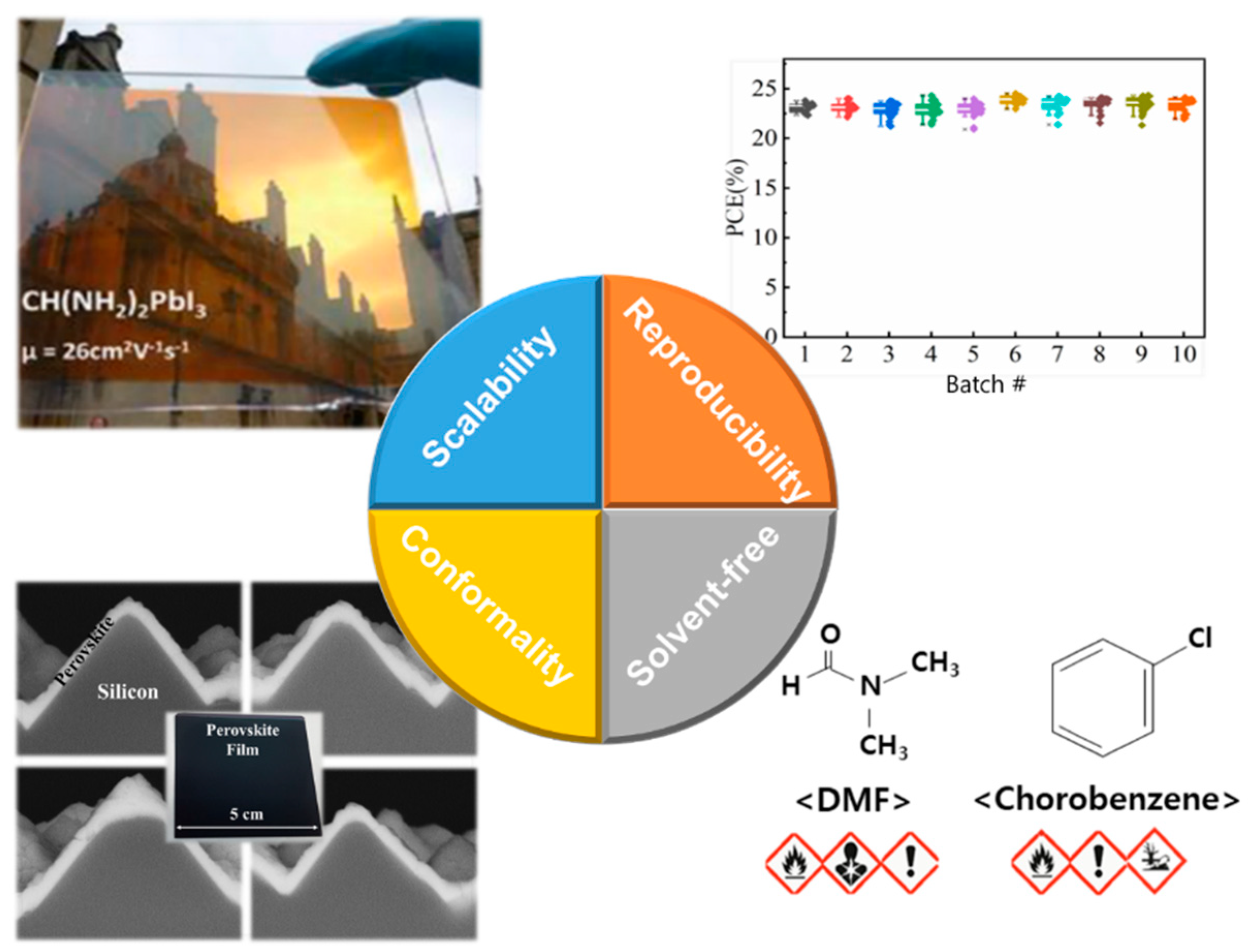
Figure 2.
The evolution of perovskite solar cell efficiencies based on solution and dry-processed perovskite deposition methods.
Figure 2.
The evolution of perovskite solar cell efficiencies based on solution and dry-processed perovskite deposition methods.
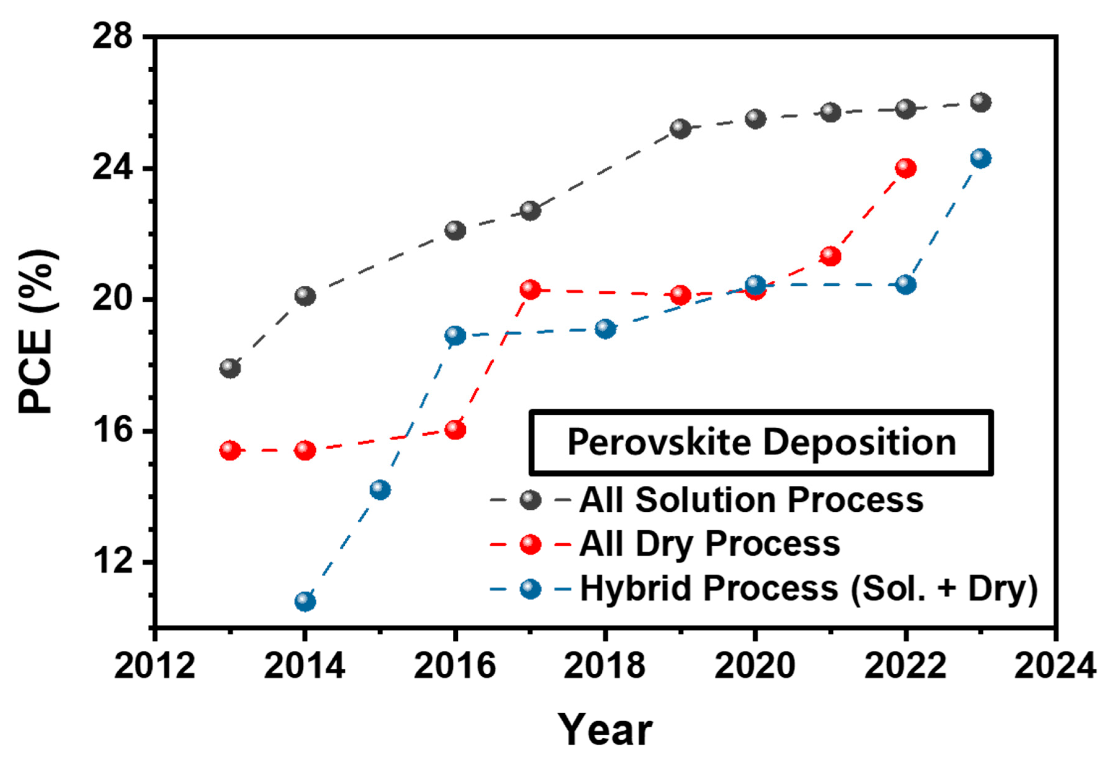
Figure 3.
(a) Schematic diagram of the triple-source co-evaporation process, and (b) light-IV curves of p-i-n perovskite solar cells (PSCs) with incorporation of excess PbI2. (Reproduced with permission from [33] American Chemical Society, Copyright 2020.) (c) Scanning electron microscope (SEM) image and (d) X-ray diffraction (XRD) analysis of a triple-cation and double-halide perovskite film. (Reproduced with permission from [32]. Wiley-VCH, Copyright 2018.) (e) SEM image of a perovskite film conformally deposited onto a silicon pyramid texture, and (f) a light-IV curve and maximum power point (MPP) measurements of PSCs with incorporation of excess formamidinium iodide (FAI). (Reproduced with permission from [35]. Wiley-VCH, Copyright 2021.) (g) Photoluminescence (PL) peak analysis with co-evaporation of phenyl ethylammonium iodide (PEAI), and (h) MPP measurements demonstrating the enhanced stability with PEAI co-evaporation. (Reproduced with permission from [37]. Wiley-VCH, Copyright 2021.) (i) Image of a MAPbI3 crystal used for single source evaporation. (j) Schematic diagram of the single-source evaporation process and (k) an XRD pattern of MAPbI3 powder and film as prepared via single-source evaporation. (Reproduced with permission from [39]. Springer Nature, Copyright 2016.)
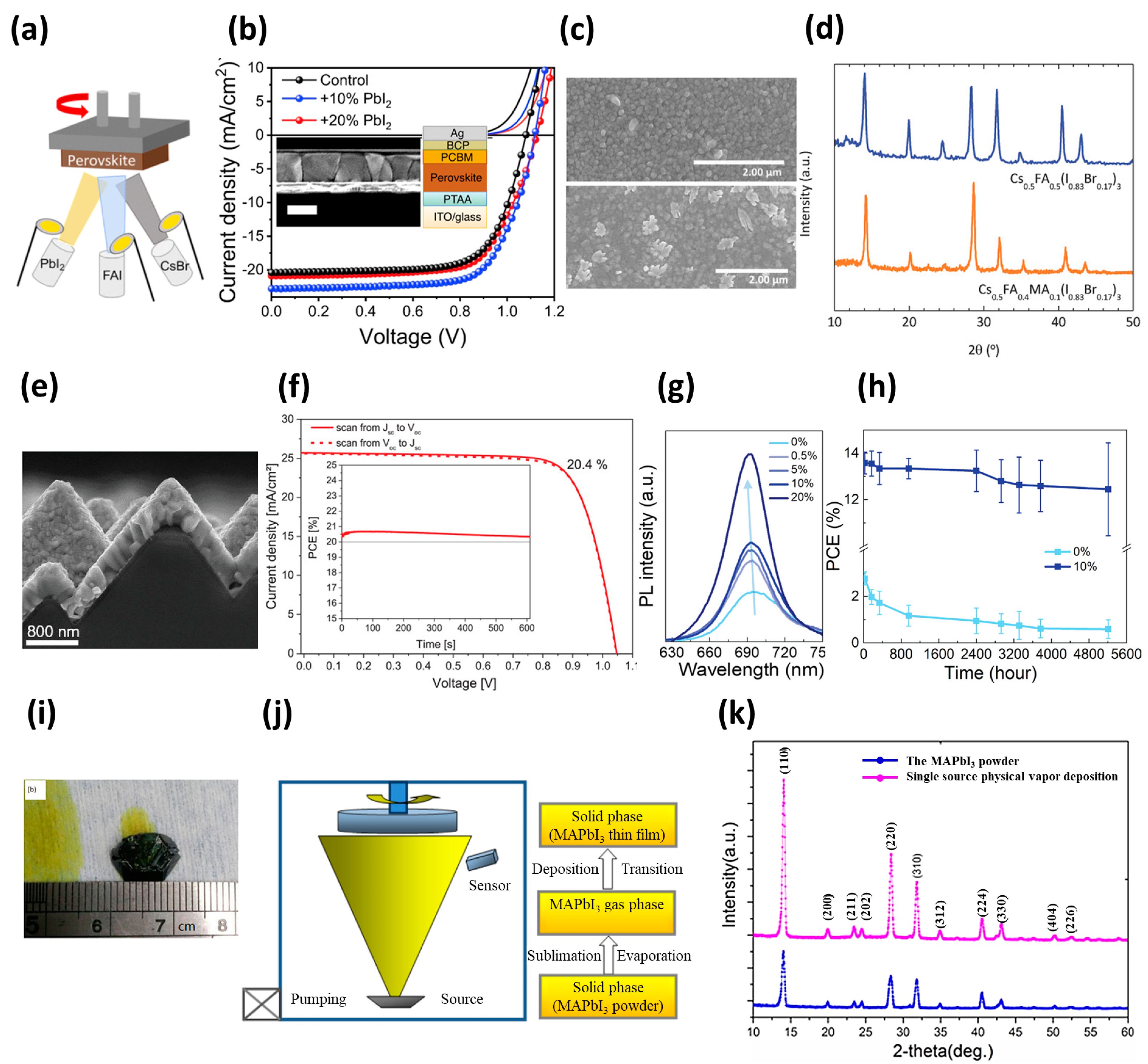
Figure 4.
(a) Schematic diagram of the sequential evaporation process and (b) SEM images of the optimized perovskite film fabricated using sequential evaporation. (Reproduced with permission from [40]. Wiley-VCH, Copyright 2014.) (c) SEM images and (d) XRD patterns of sequentially evaporated mixed organic (FAI + MAI) and lead halides (PbI2 + PbBr2). (Reproduced with permission from [43]. Wiley-VCH, Copyright 2019.) (e) Schematic of the co-evaporation of inorganic sources (PbCl2 + PbI2 + CsI) followed by sequential evaporation of organic halides (FAI) and (f) the grazing incidence wide-angle X-ray scattering pattern and (g) light-IV curves using co-evaporation with incorporation of PbCl2 followed by sequential evaporation. (Reproduced with permission from [45]. Copyright 2022, American Association for the Advancement of Science.)

Figure 5.
(a) Schematic diagram of the double-zone chemical vapor deposition (CVD) process. (Reproduced from [7] with the permission of The Royal Society of Chemistry. Copyright 2014.) (b) Champion device characteristics of perovskite solar cells fabricated by solution or CVD method. (c) Photographic images of patterned perovskite cells and modules fabricated by CVD. (Reproduced from [49] with the permission of The Royal Society of Chemistry. Copyright 2016.) (d) Effects of perovskite/SnO2 interface passivation using H2KNO3S material and (e) formation of intermediate phase and reaction energy during perovskite conversion using N-methyl-2-pyrrolidone(NMP)-PbI2. (Reproduced from [57] with the permission of Wiley-VCH. Copyright 2023.)
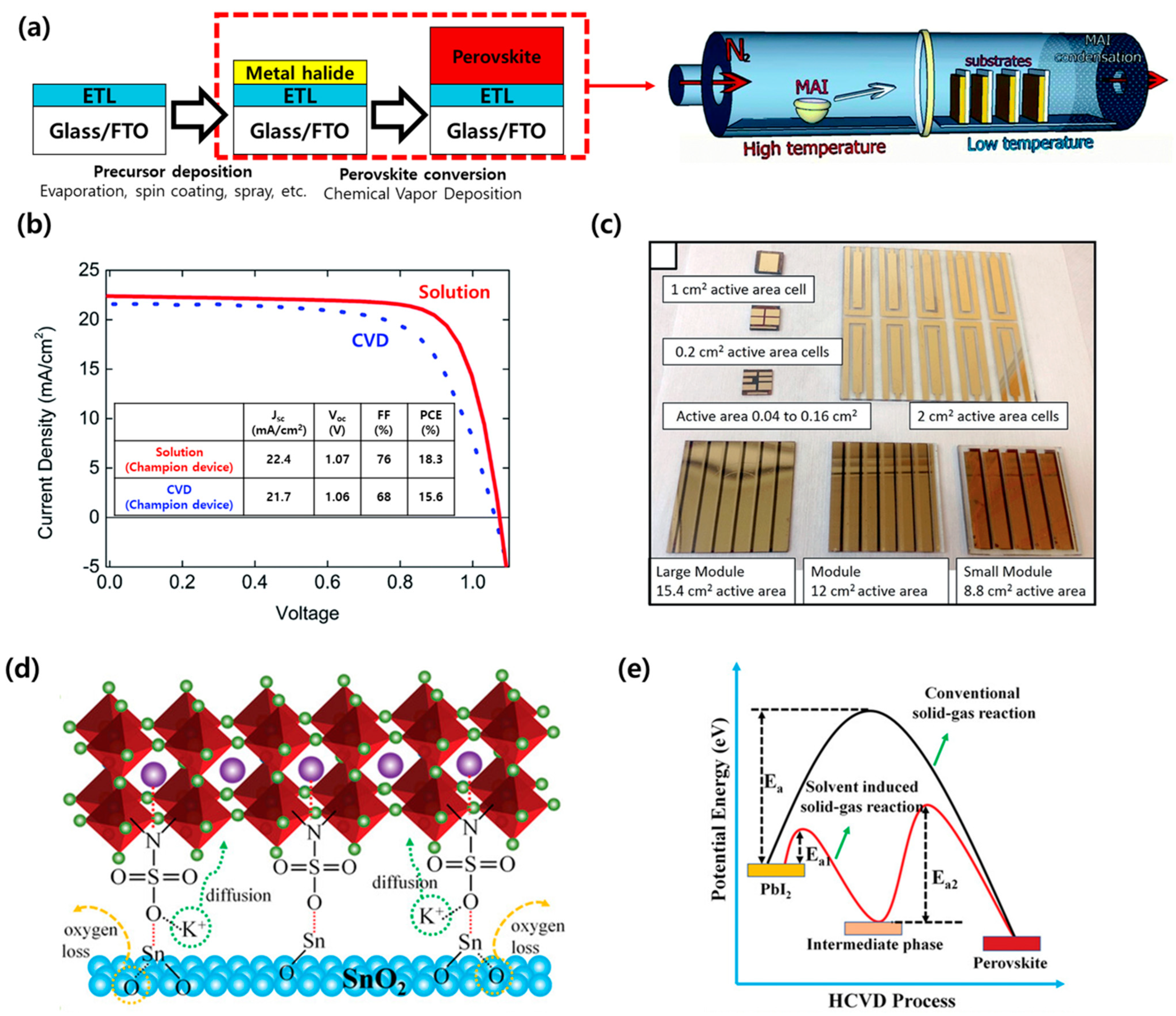
Figure 6.
(a) Schematic diagram of the single-zone CVD process. (Reproduced from [58] with the permission of Wiley-VCH. Copyright 2016.) (b) PL spectra after application of a multistage atmosphere-assisted (MSA) process and (c) surface uniformity of a perovskite film on a 64 cm2 substrate. (Reproduced from [64] with the permission of Elsevier Inc. Copyright 2021.) (d) Crystallinity of the perovskite film (XRD) and (e) surface morphology (SEM) before and after alkali ion doping. (f) Device characteristics of perovskite solar cells before and after Rb doping. (Reproduced from [65] with the permission of Wiley-VCH. Copyright 2021.)
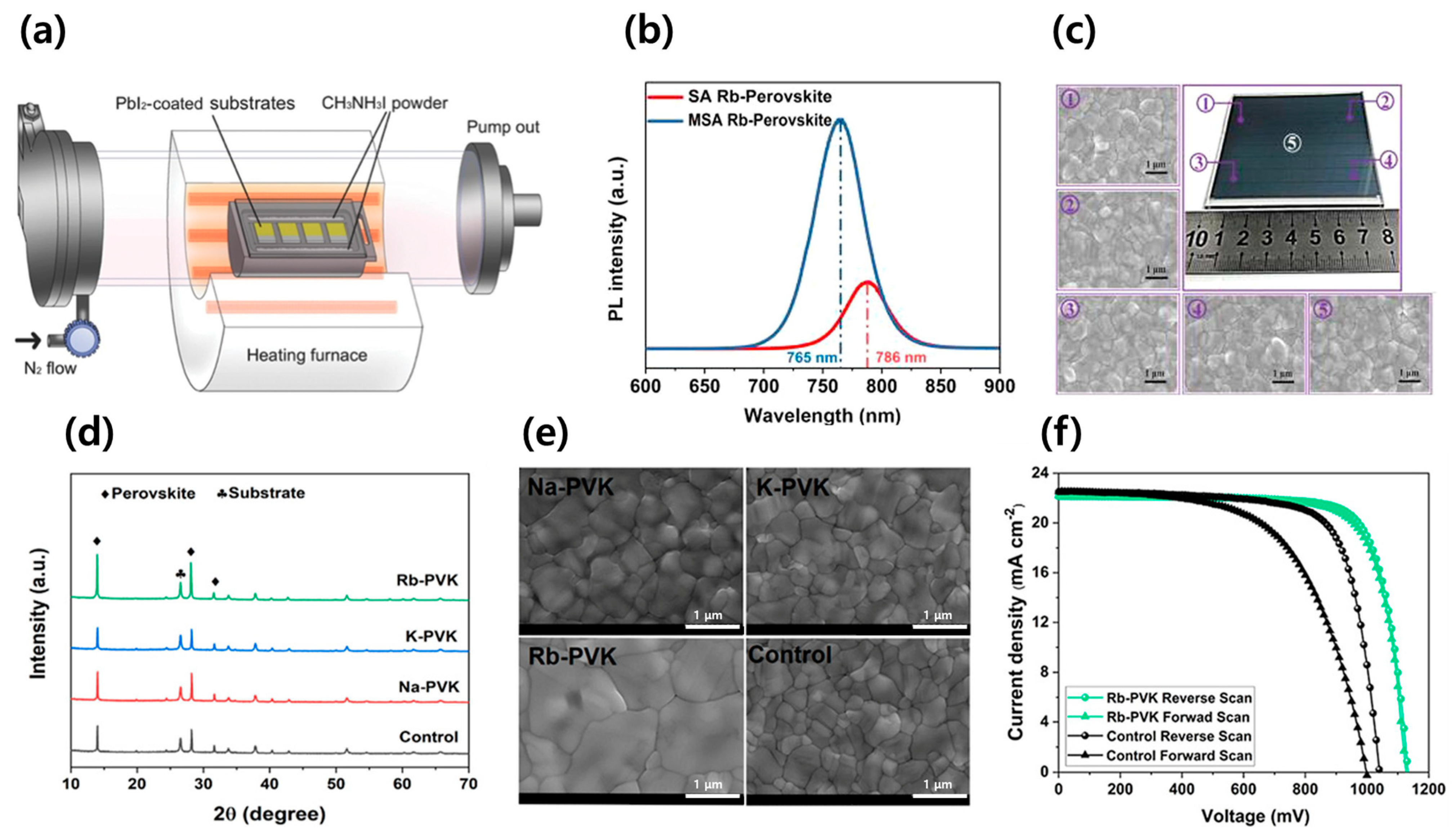
Figure 7.
(a) Schematic diagram of PbI2 sputtering and post-treatment processes and (b) comparison of perovskite solar cell characteristics before and after methylamine vapor annealing. (Reproduced from [23] with the permission of Wiley-VCH. Copyright 2023.) (c) Schematic diagram of the single-step sputtering process for MAPbI3 and (d) the effect of Cl doping and post-treatment processes on perovskite film crystallinity. (Reproduced from [90] with the permission of Wiley-VCH. Copyright 2021.) (e) Comparison of the I-V characteristics of perovskite solar cells with varying Cl doping concentration in MAPbI3. (Reproduced from [68] with the permission of the American Chemical Society. Copyright 2022.)


Table 1.
PSC properties according to deposition method.
| Device Structure | Voc (V) | Jsc (mA/cm2) | FF (%) | PCE (%) | Area (cm2) | Year | Ref. | |
|---|---|---|---|---|---|---|---|---|
| Evaporation (Co-deposition) | FTO/c-TiO2/Perovskite/Spiro-OMeTAD/Ag | 1.07 | 21.5 | 67 | 15.4 | 0.076 | 2013 | [29] |
| ITO/PEDOT:PSS/polyTPD/MAPbI3/PCBM/3TPYMB/Au | 1.09 | 18.2 | 75 | 14.8 | 0.065 | 2014 | [30] | |
| ITO/C60:Phlm/C60/MAPbI3/TaTm/TaTm:F6-TCNNQ/Ag | 1.14 | 22.08 | 80.5 | 20.3 | 0.1 | 2016 | [31] | |
| ITO/C60:Phlm/C60/Cs0.5FA0.4MA0.1Pb(I3Br0.17)3/TaTm/TaTm:F6-TCNNQ/Au | 1.146 | 17 | 82 | 16 | - | 2018 | [32] | |
| ITO/PTAA/FA0.7Cs0.3Pb(I0.9Br0.1)3/PCBM/BCP/Ag | 1.06 | 23 | 74.6 | 18.1 | 0.155 | 2020 | [33] | |
| FTO/TiO2/SnO2/PCBM/MAPbI3/Spiro-OMeTAD/Au | 1.12 | 23.3 | 77.7 | 20.28 | 0.1 | 2020 | [34] | |
| ITO/MeO-2PACz/FAxMA1–xPbI3/C60/BCP/Cu | 1.05 | 25.7 | 75.91 | 20.4 | 0.16 | 2021 | [35] | |
| ITO/Spiro-TTB/MAPbI3/PCBM/BCP/Ag/LiF | 1.13 | 22.1 | 81.3 | 20.3 | 0.086 | 2021 | [36] | |
| ITO/PTAA/CsPbI3/PCBM/BCP/Ag | 1.09 | 17.3 | 79.4 | 15 | 0.045 | 2021 | [37] | |
| FTO/SnO2/MAPbI3/Spiro-OMeTAD/Au | 1.08 | 22.7 | 78.8 | 19.3 | 0.09 | 2022 | [38] | |
| Evaporation (Sequential) | ITO/PEDOT:PSS/MAPbI3/PCBM/Ag | 0.93 | 19.47 | 60 | 10.9 | 0.09 | 2016 | [39] |
| ITO/PEDOT:PSS/MAPbI3xClx/C60/Bphen/Ca/Ag | 1.02 | 20.9 | 72.2 | 15.4 | 0.05 | 2014 | [40] | |
| FTO/c-TiO2/MAPbI3/Spiro-OMeTAD/Au | 1 | 22.27 | 72 | 16.03 | 0.071 | 2015 | [41] | |
| FTO/c-TiO2/FAxMA1–xPbI3/Spiro-OMeTAD/Au | 0.98 | 22.4 | 73 | 15.8 | 0.09 | 2019 | [42] | |
| FTO/c-TiO2/FAxMA1–xPbI3-yBry/CuPc/Au | 1.02 | 19.16 | 77.3 | 15.14 | - | 2019 | [43] | |
| FTO/c-TiO2/FAxCs1–xPbI3/Spiro-OMeTAD/Au | 1.11 | 24.88 | 77.2 | 21.32 | 0.09 | 2021 | [44] | |
| FTO/SnO2/Cs0.05FA0.95PbI3/Spiro-OMeTAD/Au | 1.15 | 25.9 | 81 | 24 | 0.1 | 2022 | [45] | |
| FTO/SnO2/CsxFA1-xPb(IyBr1-y)3/Spiro-OMeTAD/Au | 1.2 | 24.4 | 83.3 | 24.3 | 0.1 | 2023 | [28] | |
| FTO/TiO2/MAxCs1–xPbI3/Spiro-OMeTAD/Au | 1.1 | 23.17 | 79 | 20.13 | 0.09 | 2017 | [46] | |
| FTO/SnO2/Cs0.24FA0.76PbI3-yBry/Spiro-MeOTAD/Au | 1.065 | 22.88 | 71 | 17.29 | 0.16 | 2018 | [47] | |
| Chemical Vapor Deposition (Double-zone) | FTO/c-TiO2/MAPbI3–xClx/Spiro-MeOTAD/Au | 0.92 | 19.1 | 62 | 10.8 | 0.07–0.1 | 2014 | [7] |
| FTO/c-TiO2/FAPbI3–xClx/Spiro-MeOTAD/Au | 1.03 | 20.9 | 66 | 14.2 | 0.04 | 2015 | [48] | |
| FTO/TiO2/MAPbI3/Spiro-MeOTAD/Au | 0.97 | 18.0 | 64 | 11.1 | - | 2015 | [49] | |
| FTO/c-TiO2/MAPbI3–xClx/Spiro-MeOTAD/Au | 1.06 | 21.7 | 68 | 15.6 | 0.09 | 2016 | [50] | |
| FTO/c-TiO2/MAPbI3/Spiro-MeOTAD/Au | 1.06 | 22.08 | 80 | 18.9 | 0.11 | 2016 | [51] | |
| FTO/c-TiO2/m-TiO2/MAPbI3/Spiro-MeOTAD/Au | 1.00 | 23.0 | 77 | 17.6 | 0.06 | 2016 | [52] | |
| FTO/c-TiO2/CsxFA1-xPbI3/Spiro-MeOTAD/Au | 1.00 | 22.0 | 75.2 | 16.6 | 0.1 | 2017 | [53] | |
| FTO/c-TiO2/m-TiO2/MAPbI3/Spiro-MeOTAD/Au | 1.01 | 24.2 | 69 | 16.9 | 0.06 | 2018 | [54] | |
| FTO/c-TiO2/FAPbIxBr3–x/Spiro-MeOTAD/Au | 1.03 | 21.1 | 74 | 16.1 | 2 | 2019 | [55] | |
| FTO/c-TiO2/FA0.93Cs0.07PbI3/Spiro-MeOTAD/Au | 0.99 | 22.3 | 70.2 | 15.5 | 0.1 | 2020 | [56] | |
| ITO/SnO2/H2KNO3S/Cs0.05FA0.5MA0.45PbI3/Spiro-MeOTAD/Au | 1.15 | 23.93 | 80 | 21.98 | 0.09 | 2023 | [57] | |
| Chemical Vapor Deposition (Single-zone) | FTO/c-TiO2/MAPbI3/Spiro-MeOTAD/Au | 0.972 | 21.15 | 75 | 15.37 | 0.24 | 2016 | [58] |
| FTO/c-TiO2/C60/(FA)x(MA)1–xPbI3/Spiro-MeOTAD/Au | 1 | 22.51 | 73.56 | 16.48 | 0.09 | 2017 | [59] | |
| FTO/c-TiO2/m-TiO2/(PEA2MAn-1PbnI3n+1)/Spiro-MeOTAD/Au | 1.08 | 21.91 | 80.36 | 19.1 | 0.2 | 2018 | [60] | |
| FTO/c-TiO2/Cs0.15FA0.85PbI2.85Br0.15/Spiro-MeOTAD/Au | 1.06 | 22.82 | 75.4 | 18.22 | 0.09 | 2018 | [61] | |
| FTO/c-TiO2/Cs0.1FA0.9PbI3/Spiro-MeOTAD/Au | 0.99 | 22.87 | 74.82 | 16.39 | - | 2019 | [62] | |
| FTO/c-TiO2/C60/(PEA2MAn-1PbnI3n+1)/Spiro-MeOTAD/Au | 1.08 | 23.75 | 70.4 | 18.08 | - | 2020 | [63] | |
| FTO/SnO2/Rb0.04Cs0.14FA0.86Pb(BryI1-y)3/Spiro-MeOTAD/Au | 1.127 | 22.63 | 76.8 | 19.59 | 0.148 | 2021 | [64] | |
| FTO/SnO2/Rb0.04Cs0.14FA0.86Pb(Br0.03I0.97)3/Spiro-MeOTAD/Au | 1.13 | 22.2 | 78 | 19.6 | 0.16 | 2021 | [65] | |
| Sputtering | FTO/NRT/MAPbI3/Spiro-MeOTAD/Au | 1.04 | 20.2 | 66.9 | 14.1 | 0.09 | 2017 | [66] |
| FTO/TiO2/MAPbI3/Spiro-MeOTAD/Au | 0.856 | 22.1 | 53.8 | 10.2 | 0.075 | 2020 | [67] | |
| FTO/TiO2/MAPbI3/Spiro-MeOTAD/Au | 0.791 | 19.5 | 71.2 | 11.1 | 0.078 | 2020 | [22] | |
| FTO/c-TiO2/m-TiO2/MAPbI3-xClx/Spiro-MeOTAD/Au | 0.97 | 22.53 | 71 | 15.52 | 0.06 | 2021 | [23] | |
| FTO/TiO2/MAPbI3/Spiro-MeOTAD/Au | 0.98 | 22.96 | 76 | 17.1 | 0.08 | 2022 | [68] | |
| FTO/TiO2/MAPbI3/Spiro-MeOTAD/Au | 0.86 | 23.4 | 60.3 | 12.2 | 0.075 | 2023 | [69] |
Disclaimer/Publisher’s Note: The statements, opinions and data contained in all publications are solely those of the individual author(s) and contributor(s) and not of MDPI and/or the editor(s). MDPI and/or the editor(s) disclaim responsibility for any injury to people or property resulting from any ideas, methods, instructions or products referred to in the content. |
© 2023 by the authors. Licensee MDPI, Basel, Switzerland. This article is an open access article distributed under the terms and conditions of the Creative Commons Attribution (CC BY) license (https://creativecommons.org/licenses/by/4.0/).
Share and Cite
MDPI and ACS Style
Hwang, J.-K.; Jeong, S.-H.; Kim, D.; Lee, H.-S.; Kang, Y. A Review on Dry Deposition Techniques: Pathways to Enhanced Perovskite Solar Cells. Energies 2023, 16, 5977. https://doi.org/10.3390/en16165977
AMA Style
Hwang J-K, Jeong S-H, Kim D, Lee H-S, Kang Y. A Review on Dry Deposition Techniques: Pathways to Enhanced Perovskite Solar Cells. Energies. 2023; 16(16):5977. https://doi.org/10.3390/en16165977
Chicago/Turabian StyleHwang, Jae-Keun, Seok-Hyun Jeong, Donghwan Kim, Hae-Seok Lee, and Yoonmook Kang. 2023. "A Review on Dry Deposition Techniques: Pathways to Enhanced Perovskite Solar Cells" Energies 16, no. 16: 5977. https://doi.org/10.3390/en16165977
Note that from the first issue of 2016, this journal uses article numbers instead of page numbers. See further details here.