Abstract
There has been a recent surge in interest toward thin film-based solar cells, specifically new absorber materials composed by Earth-abundant and non-toxic elements. Among these materials, antimony selenide (Sb2Se3) is a good candidate due to its peculiar properties, such as an appropriate bandgap that promises a theoretical maximum power conversion efficiency of 33% and an absorption coefficient of around 105 cm−1, enabling its use as a thin film absorber layer. However, charge carrier transport has been revealed to be problematic due to its cumbersome structure and the lack of a doping strategy. In this work, we aim to provide a clear picture of the state-of-the-art regarding research on Sb2Se3-based solar cells and its prospects, from the successful achievements to the challenges that are still to be overcome. We also report on the key parameters of antimony selenide with a close focus on the different characteristics associated with films grown from different techniques.
1. Introduction
The continuous growth of global electricity demand and the recognition of the serious consequences of climate change due to CO2 emissions continue to give impetus to research on renewable energies and on photovoltaics. In 2022, 63.3% of global energy demand was supplied by fossil fuels, 26.3% was supplied by renewables and 10.4% was supplied by nuclear fission. Among renewables, the leading energy supplier remains hydropower with 15.8%, and while solar photovoltaic makes up just 2.7% of the global energy production, this figure is rapidly increasing [1]. Theoretical calculations show that 1 kW power produced by photovoltaics would reduce CO2 emissions into the atmosphere by 1 ton/year compared to that produced by fossil sources. Furthermore, the total energy needed by all humanity would be met if only ~0.05% of the Earth’s crust were covered by photovoltaic modules with an average efficiency of 20% [2,3]. Although this estimate is purely theoretical and overly simplistic, it gives an approximate idea of the ability that is required of solar photovoltaic to satisfy the global growth of energy demand.
Today, the main technologies for producing inorganic materials for terrestrial photovoltaic purposes are the following:
- Bulk technology;
- Epitaxy;
- Thin film technology.
The bulk technology for photovoltaics (PVs) concerns modules based on silicon single-junctions, both monocrystalline (m-Si) and polycrystalline (p-Si). Nowadays, Si-based cells lead the market with commercial modules showing power conversion efficiency (PCE) of up to 22%. Meanwhile, at a laboratory scale, m-Si and p-Si show a efficiencies of 26.1% and 23.3%, respectively [4]. The huge drawcard of Si-based technology lies in the fact that silicon is a non-toxic, abundant element in the Earth’s crust, and the technology was first developed on an industrial level driven by the production of chips for the electronic market. Moreover, Si-based solar modules exhibit a long-term stability in terms of device performance [5]. Despite these factors, the production costs of Si-based devices remain high due to the need for high-purity solar-grade silicon (9N purity) [6]. Although the Czochralski growth method was successfully implemented and refined for large-scale Si production, the high temperature and small production rates make this technology energy consuming [7,8,9]. Moreover, silicon, being an indirect bandgap semiconductor [10], has a relatively small absorption coefficient (α ~ 102–104 cm−1) in the visible region of the solar spectrum [11] and needs to be at least 100 µm thick to absorb the whole visible spectrum [12,13].
PV cells belonging to the epitaxial family are usually multijunction cells based on GaAs and its derivatives [14,15,16]. Growth techniques suitable for epitaxy slow deposition rates (~0.1 Å/s) are Molecular Beam Epitaxy (MBE), Atomic Layer Deposition (ALD) and Chemical Vapor Deposition (CVD), including their variants, such as Plasma-Enhanced CVD (PECVD) and Metal–Organic CVD (MOCVD) [17].
A world record has been achieved with a six-junction (6-J) cell based on III–V semiconductors, reaching a PCE of 37.9% and 47.1% under 1 Sun and under a x143 concentration system, respectively [18,19].
From the industrial scalability point of view, the main disadvantages are the following:
- The high cost of the crystalline substrate on which GaAs is grown, typically germanium [20], whose role is crucial since its lattice structure and crystal orientation strongly influence those of the growing thin film [21];
- The difficulty of cost-effectively transferring the epitaxial layer away from the substrate [22].
On the contrary, thin film technology (TF) refers to techniques which do not have the ambition to form single crystals, such as High-Vacuum Thermal Evaporation (HVTE), Close-Spaced Sublimation (CSS) and Sputtering [23,24,25,26,27]. The biggest advantage for the first two techniques is the high deposition rate (up to ~1 µm/min), which makes them interesting from an industrial point of view. Indeed, the sputtering system was industrially developed for a wide range of applications such as the metallization of integrated circuits [28,29], anti-corrosion coatings [30], optical coatings [31], glass coatings [32] and finally solar cells [33], well before being taken to research and technological development laboratories.
From the second half of the 1900s, thin film technology was studied to try to overcome the drawbacks related to the crystalline Si-based solar cells. Starting from the Cu2S/CdS system, a PCE of 8.5% was achieved [34,35,36]. Despite that, the stability and the ratio between the efficiency and the production costs were not helpful compared to silicon technology [37]. Other technologies have been developed, such as amorphous silicon (a-Si) and Cu2ZnSnS4 (CZTS), and commercialized, such as Cu(In,Ga)Se2 (CIGS) and CdTe [38,39,40], but without being able to really contest the leadership of bulk Si technology.
In recent years, antimony chalcogenide materials such as Sb2Se3 (ASe), Sb2S3 and Sb2(S,Se)3 have attracted great attention as possible candidates to replace the more traditional absorber materials in thin-film photovoltaic technology (CdTe and CIGS) [41,42,43,44,45,46]. Indeed, these emerging materials present many advantages being Earth-abundant and non-toxic, contrarily to Cd- and Te- or In-based solar cells [47,48,49].
In the last ten years, research on Antimony Selenide (ASe), for photovoltaic purposes, has undergone a sharp increase both in terms of the number of publications and of solar cell efficiencies (see Figure 1). Despite the advantages and the continuous progress made recently to improve the efficiencies of the Sb2Se3-, Sb2S3- and Sb2(S,Se)3-based solar cells, having reached record efficiencies of 10.5%, 7.5% and 10.7%, respectively [50,51,52], there is still a long way to go before competing with CdTe and CIGS-based solar cells (PCECdTe ≈ 22.1%, PCECIGS ≈ 23.4%) [53].
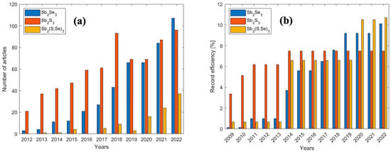
Figure 1.
(a) Number of research articles per year related to antimony selenide (blue), antimony sulfide (orange) and antimony selenosulfide (yellow). The data have been acquired by means of the Clarivate search engine; (b) Efficiency record of solar cells based on Sb2Se3 [50,54,55,56,57,58,59,60,61], Sb2S3 [52,62,63,64] and Sb2(S,Se)3 [51,54,65,66,67].
The road to reach the 10% efficiency milestone started in 2009 when a working solar cell, with a chemical bath-deposited absorber (CBD), was reported to have a PCE of 0.13% [54]. Two years later, a layer of PbSe was added to the Sb2Se3-based device to increase the short circuit current, reaching a PCE of 0.99% [55]. It was only in 2014 that greater efficiency was reached by depositing ASe through thermal evaporation (TE) followed by heat treatment at 200 °C in Se-atmosphere, yielding a PCE of 3.7% [56]. By employing Rapid Thermal Evaporation (RTE), allowing single crystalline grains to grow with a favorable preferential orientation, Zhou and coworkers reached a PCE of 5.6% in 2015 [57]. In 2017, a PCE of 6.5% was reached by employing colloidal quantum dots as hole-transporting materials [58]. One year later, a further increase in efficiency was achieved for this system by depositing antimony selenide by Vapor Transport Deposition (VTD), with a PCE of 7.6% [61]. In 2019, a PCE of 9.2% was reached depositing ASe by Close-Spaced Sublimation (CSS), obtaining a nanorod array structure [59]. The 10% efficiency wall has been broken, as mentioned above, in two papers from 2022: in one case, ASe was deposited by CBD in a superstrate configuration, utilizing thiourea and selenourea as additives to manipulate the reaction kinetics and improve the quality of the film. The resulting layers were Se-rich, and the improvement in efficiency was attributed to the reduction in antisites defects [50]. In the other case, ASe was deposited by Injection Vapor Deposition (IVD), a technique that is reported to produce layers with fewer trap states, suppressing carrier recombination [60]. In 13 years, an encouraging ~80-fold improvement in efficiency has been reached, fostering hopes for the commercial viability of Sb2Se3 based solar cells.
Researchers focused mainly on the absorber material, and since the first articles, it was clear that the absorber deposition technique plays a fundamental role in the crystalline quality of the material.
Apart from the absorber, great efforts have been dedicated to the study of the back-contact ohmic behavior [68,69,70] and, in superstrate solar cell configuration, the study of the best window material on which ASe grows to form the p/n junction [71,72,73,74].
Herein, Sb2Se3-, Sb2S3- and Sb2(S,Se)3-based solar cells will be the main subject of this review article. A detailed description of the materials, such as structural properties, optical and energetical properties, defects, transport and recombination, will be presented. Possible paths to better exploit ASe PV capabilities will be discussed, focusing on ways to reduce the material defects, as well as improving the quality of the interface with the n-type partner. Controlling the structural defects will allow an improvement of charge transport and reduction in charge carrier recombination, boosting the open circuit voltage (Voc) and the Fill Factor (FF). Doping strategies to increase the intrinsic low carrier density of ASe will also be discussed. Furthermore, possible materials able to substitute the more common CdS will be considered, aiming for a more sustainable cadmium-free device.
2. Properties
2.1. Structural Properties
Antimony selenide is part of a family of isostructural compounds of the A2B3 type (A = Bi, Sb and B = S, Se), which are part of the wider AVm–BVIn group [75,76]. The lattice space group has been reported as either Pbnm with cell dimensions a = 11.62, b = 11.77 and c = 3.962 Å or Pnma with cell dimensions a = 11.7938, b = 3.9858 and c = 11.6478 Å [77,78]. Both space groups refer to the same orthorhombic crystal structure, since the only difference is the permutation of the axis. Later in the text, we refer every spatial direction to the Pbnm space group. The main feature of Sb2Se3 is its one-dimensional nature, being made with repetitive (Sb4Se6)n chains oriented along the c-axis. These ribbons are weakly bonded together by van der Waals interactions along the (010) planes forming sheets that are held together by even weaker bonds perpendicular to the (010) planes. The interatomic distance between the ribbons is quite large (2.98 Å), and the distance between the sheets is determined by two Sb-Se bonds of 3.46 and 3.74 Å [77].
There are two nonequivalent positions for antimony and three for selenium atoms. Sb(1) atoms are six-coordinated with one Se(3) and two Se(2) atoms at short distances and with one Se(2) and two Se(1) atoms at longer distances. This configuration results in a heavily distorted octahedron around Sb(1) with three longer and three shorter Sb-Se distances. Sb(2) atoms are instead seven-coordinated with one Se(1) and two Se(3) atoms at shorter distances, two Se(1) atoms at medium distance and finally with two Se(2) atoms at longer distances. Sb(2) sits at the center of the rectangle formed by two Se(1) and two Se(3) atoms which is the base of a tetragonal pyramid whose vertex is another Se(1) atom. Two pyramids around Sb(2) are linked together via Se(2) atoms forming a double polyhedron, which is further linked to other two octahedrons around Sb(1) via Se(3) atoms (see Figure 2c) [78].
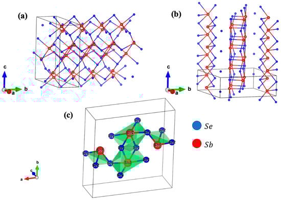
Figure 2.
Sb2Se3 crystal structure that refers to (a) Pnma and (b) Pbnm space group expanded along the ribbon direction. (c) the non-equivalent positions of Sb and Se atoms are presented considering the Pbnm space group, bonds are depicted only between short- and medium- distance atoms. All figures are made with VESTA software 3.5.8 [79].
This peculiar quasi-1D structure makes ASe a strongly anisotropic material where charge transport is made difficult in the directions perpendicular to the c-axis (the ribbon axis). Therefore, the mobility of both the charge carriers in this material is small (as well as its conductivity, as seen in Table 1) and seldom reported in the literature, since it is difficult to measure with traditional Hall experiments.
2.2. Optical Properties and Band Structure
Among the A2B3 chalcogenides, Sb2Se3 is the most efficient PV absorber material, and its exceptional optoelectronics properties have initially attracted the attention of the research community looking for a new absorber material for solar cells. Indeed, by considering the spectroscopic limited maximum efficiency [80], a figure of merit born from a generalization of the Shockley–Queisser limit, ASe, could far outperform both CdTe and CZTS [73], which are two of the most advanced thin film solar technologies.
A first step to study a new absorber material is to precisely measure its fundamental optical parameters such as the energy gap (both direct and indirect), the complex refractive index and the dielectric constants for each wavelength of the visible spectrum. Even though many efforts were dedicated to this task, there is still a wide range of figures circulating in the literature on the ASe optical constants, as can be seen in Figure 3. This is likely a direct consequence of the great variety of deposition techniques employed to deposit thin films of this highly anisotropic material without being able to achieve a low defect density (here and in the following, we mean the spatial density). Indeed, each deposition technique produces thin films with different preferential orientations and grain dimensions; thus, the optical measurements of films deposited with different techniques cannot be directly compared.
The first report on the optical properties of Sb2Se3 was produced by El-Shair et al. [81]. The authors used optical transmittance data measured on Sb2Se3 amorphous thin films, deposited by evaporation at room temperature on a quartz substrate, to evaluate the refractive index and extinction coefficient on a wide spectral range. Samples with thicknesses up to 764 nm were analyzed, and both coefficients were found to be independent of the film thicknesses. Afterward, the films were annealed at different temperatures and XRD peaks related to ASe appeared, with intensities proportional to the annealing temperatures, signaling an amorphous to crystalline phase transition. At the same time, the optical constants increased across the spectral range examined with increasing annealing temperatures. The absorption coefficient had an encouraging value over 104 cm−1; the reported high refractive index, between 3 and 4, may require an antireflection coating to reduce reflection in future optimization. Both direct and indirect optical transitions were observed at 1.91 and 1.225 eV, respectively. Both the direct and indirect energy-gap reduced considerably after annealing up to a temperature of 200 °C, reaching values of 1.54 and 1.1 eV, respectively [81]. These initial results have been only partially confirmed by succeeding studies employing spectroscopic ellipsometry. In particular, the red shift of the bandgap, after annealing at increasingly higher temperatures, has been reported also for film deposited by sputtering [82], thermal evaporation [83,84,85] and PLD [86] and attributed to the better crystallization of the material. The same is true for the values of the optical constants that increase along the whole spectrum, with the increase in the annealing temperatures and crystallinity [85]. In contrast, in a more recent study on crystalline films, both refractive index and extinction coefficient were reported to increase with thickness (up to 429 nm) due to normal dispersion and the increase in carrier concentration [84]. This behavior was also recently seen in amorphous films deposited by sputtering with thickness ranging from 176 to 1155 nm [87]. In this case, the authors based their explanation by considering the change of the film stoichiometry with different thicknesses, since Se tends to vaporize faster when the deposition takes longer. Recent reports on highly crystallized films of ASe find very small energy difference between direct and indirect optical transitions, which is why Sb2Se3 is now mostly considered a direct energy gap semiconductor. Chen et al. used a variety of different techniques to study the optical properties of both amorphous and crystalline films [83]. Ellipsometry, the Swanepoel method and photoluminescence were employed to measure the optical constants, while transmission spectra at different temperatures were performed to observe the change from indirect to direct optical transition at low temperatures. ASe is an intrinsically indirect semiconductor already at 150 K, with close direct and indirect energy bandgaps of 1.03 and 1.17 eV respectively. The crystalline samples present higher values for n and k than the amorphous ones, and the refractive index follows a normal Cauchy-type dispersion for longer than infrared wavelengths. The dielectric constant turns out to be quite large along the ribbon direction (≈19) in the crystalline sample, which is greater than in the amorphous one (≈16), suggesting a small exciton binding energy (even smaller than for CIGS [88]) that favors the immediate separation of the photogenerated carrier. Moreover, density functional theory (DFT) simulations reported that the dielectric tensor exhibits a huge anisotropy (εxx = 15.43, εyy = 10.69 and εzz = 15.46), with the highest value in the ribbon direction, reflecting again that this direction is the favorite in terms of charge transport, since the carriers are more shielded from dispersion and recombination [89].
Regarding the nature of the optical bandgap, some authors have reported that only direct transitions are seen at room temperature [82,84,87,90,91], while others state that only indirect transitions are observed [83,92,93,94] and still others claim that both are detected [81,95,96]. This ambiguity will remain due to the Sb2Se3 electronic band structure. Indeed, even though many simulations employing either DFT [89,97,98] or the pseudo-potential plane waves method [99] found that ASe is an indirect semiconductor with an energy gap between 0.95 and 1.3 eV, there is still a high chance of direct transitions, since the direct and indirect energy bandgaps differ by only tens of meV. Another common finding of theoretical calculations on Sb2Se3 is the vicinity of the valence band maximum to the conduction band minimum in the reciprocal space, thus requiring only a small momentum exchange for the electron transition [97] which would explain the low temperature needed to suppress indirect transitions found by Chen et al [83].
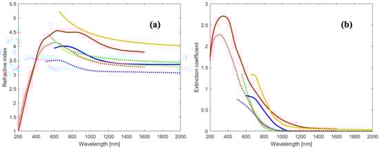
Figure 3.
(a) Refractive index and (b) extinction coefficient from articles focused on the optical properties of ASe (red [83], blue [81], orange [85], green [87]). Dotted lines refer to amorphous films, while continuous lines refer to crystalline films.
Different methods can be performed to tune the optical characteristics of ASe, the most straightforward of which are selenization and sulfurization.
Razykov et al. deposited crystalline Sb2Se3 thin films by chemical molecular beam deposition, achieving large grain sizes, and they found that a lower content of Se increases the bandgap from 1.09 to 1.17 eV, passing from 0.85 to 0.66 of the Sb/Se ratio [90]. This bandgap increase after selenization has been reported also by others [56], and for amorphous films, the energy gap has been reported to follow a Vegard-type law with different Se content [95]. This suggests that an improvement in the crystallinity and stoichiometry of the films via selenization could explain the red-shift phenomenon presented above, since many of the produced ASe films are Se-poor. Selenization is found to be effective for defect management, as we will analyze in the next section dedicated to defects in ASe.
Sb2S3 has an energy bandgap of around 1.7 eV, which is considerably larger than that of Sb2Se3, and the two compounds are isostructural, with both S and Se part of the same group of the Mendeleev’s table. It is therefore not surprising that an alloy of the two compounds exists as a solid solution with any concentration of sulfur and selenium. Sulfurization seems to be a practical route to enhance the Voc of ASe-based solar cells [100], which has already given good results by achieving high PCEs in a short time [51], although it must be noted that the research on this new material benefited from the huge jumpstart gifted from the established academic literature on ASe solar cells.
El Sayad et al. have for the first time successfully alloyed Sb2Se3 with Sb2S3, producing amorphous thin films of Sb2SxSe3−x with different concentrations of the two chalcogenides (x = 0, 1, 2, 3) [101]. As expected from Vegard law [102], the energy gap of the film increases with the increase in the sulfur content, following an empirical quadratic equation. The optical coefficients were extrapolated using the Swanepoel method, from transmittance measurements, show intermediate values between that of Sb2Se3 and Sb2S3, meaning they both decrease with sulfur content. In a follow-up study, after annealing, the optical properties at different temperatures of the same films were examined [85]. As the sulfur content increases, the system requires increasingly higher temperatures to undergo phase transition from amorphous to polycrystalline, since the distortions introduced in the lattice need more thermal energy to adjust. In amorphous films of Sb2SxSe3−x with x > 2, increasing the annealing temperature has no effect until decomposition. The antimony selenosulfide crystallized film shows a direct bandgap transition with larger values than that of ASe, which instead shows both indirect and direct transitions.
Although solid solutions are possible for any value of sulfur concentration, a change in the bandgap is not the only effect that should be expected. In fact, a photoluminescence study showed that when the sulfur content is low, the photoluminescence (PL) emission has excitonic origins, while at higher sulfur content, the emission stems from deep donor to deep level recombination, implying that the primary recombination mechanism changes after a certain sulfur concentration threshold [103].
2.3. Defects in Antimony Selenide
The typical defects that occur in polycrystalline thin film are recombination centers at the grain boundaries [104,105]. In antimony selenide, as already discussed, the preferential orientations suitable for PV purposes are along the (h, k, l) planes with l ≠ 0, because the grains grow parallel to the ribbon directions with a reduction in the recombination process at the interface between ribbons. In fact, it has been reported that if the grains grow along those directions, grain boundaries are intrinsically passivated because they exhibit the (hk0) planes that are considered free of dangling bonds [57].
Concerning the study of point defects in ASe, the expectation of earlier DFT simulations were overly optimistic, since it was believed that for such a simple monophase binary compound with a low symmetry structure, only five defects could exist: two vacancies (VSe and VSb), two antisites (SbSe and SeSb) and only one interstitial (Sei) [106]. The root of this supposition comes from the study of precedent semiconductors like GaAs and CdTe. In fact, contrary to these high-symmetry semiconductors, the quasi 1D structure of ASe renders the specific non-equivalent site of the defect of particular importance on both its ionization energy and its formation energy. Moreover, as was pointed out before, interatomic distances in Ase are large, and this allows the structure to endure heavy deformation, so much so that later DFT works have even considered the possibility of double antisite (2SeSb) formation [107]. These complications are the cause of a large number of point defects, which are now considered in theoretical papers and count as many as five types of vacancies (VSe1, VSe2, VSe3, VSb1, VSb2), five type of antisites (SbSe1, SbSe2, SbSe3, SeSb1, SeSb2) and many interstitial defects. The effect of the latter are not yet understood, as some articles reported them to be unimportant, either because their formation energy is too high [107] or their ionization energy levels are too deep [108] to influence the electronic properties of ASe, while others classify them as detrimental midgap trap states [89].
In antimony selenide, being a simple binary compound, two limit conditions can be achieved during deposition. These conditions are the limit cases considered in DFT simulations:
- Se-rich conditions (Sb/Se ratio < 0.66);
- Sb-rich conditions (Sb/Se ratio > 0.66).
VSe and VSb are the most studied defects. VSb are reported as either deep [109] or shallow [110] acceptors and should be the natural source for the p-type nature of ASe although, in a DFT simulation, Stoliaroff et al. reported that their enthalpy of formation is very high; therefore, their concentration cannot be directly correlated with the concentrations of VSe that are considered deep donor defects [108].
Indeed, selenium vacancies are almost universally considered detrimental to the performance of ASe solar cells since they act as donor defects, reducing the already small number of free holes [61,89,111,112,113].
SeSb and SbSe antisites may derive from the dual cationic and anionic nature of Sb, which allows the substitution with Se atoms. In general, the nature of SbSe defects is debated if they act as acceptor or donor (deep donor in case of Se-poor condition) levels due to the amphoteric nature of Sb, and they are present in three different types [108,114]. More precisely, antimony placed in the crystallographic site 2 can substitute selenium positioned in sites 1 and 2, forming two acceptor levels at 0.33 eV and 0.40 eV from the valence band, respectively. Antimony, located in site 1, can form a Sb1Se3 defect, which exhibits an energy level just above the maximum of the valence band at 0.23 eV. This type of defect presents a formation energy lower than that of the VSe hole killer, hence providing the weak p-type conduction to Sb2Se3. On the other hand, SeSb is a deep donor level, whose action is not very effective on the conduction mechanism, given that Sb2Se3 naturally shows a weak p-type conduction, as said before [106,108].
Deep level transient spectroscopy (DLTS), admittance spectroscopy at different DC bias and resistivity measurements as a function of temperature were performed to study the correlation between defects and energy levels into the energy gap of Sb2Se3. Three types of defects have been observed, corresponding to the following energy levels: D1 ≈ 300 meV, D2 ≈ 400 meV and D3 ≈ 600 meV measured starting from the bottom of the conduction band [115]. The D1 energy level can be associated with donor defects due to SbSe and/or VSe [106], D2 is related to VSb or to SeSb1 and acts as a hole trap [115,116], while the D3 level refers to the SbSe defect and has an electron trap behavior [114]. Moreover, the photovoltaic parameters of Sb2Se3-based solar cells are strongly dependent on the near mid-gap D1 and D2 levels. These levels vary slightly in energy, causing the variation of the behavior of the solar cell. Conversely, D3 being typically constant could be related to the interface only [117]. Furthermore, in Se-rich Sb2Se3 films, the Hall effect and resistivity versus temperature measurements have identified a shallow acceptor level with an energy of 120 meV, and this defect is attributed to SeSb [118].
Native defects, formed between Sb2Se3 and the n-type partner, with which it forms the p-n junction, are mainly due to a non-perfect band alignment and the lattice mismatch. For this reason, they are the first suspects responsible for the limited Voc (∼500 mV) in Sb2Se3-based solar cells [119,120,121].
Strategies to tune and control defects in ASe are still lacking. Selenization treatment has been performed to reduce the density of VSe and improve the density of holes with moderate success, but the Voc deficit remains high [121,122,123,124].

Table 1.
Material properties of ASe deposited with different techniques. Optical constant values refer to the bandgap energy, while τ refers to the lifetime of the minority carrier. Deposition technique acronyms refer to the following processes: Rapid Thermal Evaporation (RTE), Radio Frequency Magnetron Sputtering (RFMS), Spin Coating (SC), Chemical Bath Deposition (CBD), Hydrazine Solution Process (HSP), Vapor Transport Deposition (VTD), and Thermal Evaporation (TE).
| Sb2Se3 | Deposition Techniques | Ref. | |
|---|---|---|---|
| Density (g cm−3) | 5.84 | - | [125] |
| Melting point (K) | 885 | - | [125] |
| Conductivity (Ω−1 cm−1) | 2.5 × 10⁻⁵–6.7 × 10⁻⁷ | RTE; RFMS | [126,127,128] |
| Eg (eV) | 1.02–1.26 | SC; RTE; RFMS; CBD | [58,92,111,112,129] |
| χ (eV) | 3.9–4.15 | HSP; RFMS | [58,111,112,129] |
| NA (cm−3) | 3.0 × 10¹³; 2 × 10¹⁴ | HSP; RFMS | [129] [58] |
| Nv (cm−3) | 1.8 × 10¹⁹; 1.5–1.8 × 10²⁰ | RTE; VTD | [130] [91] |
| Nc (cm−3) | 2.2 × 10¹⁸; 1.4 × 10¹⁹; 1 × 10¹⁸ | RTE; VTD; RFMS | [130] [91] [58] |
| Nt (cm−3) | 1.6–13 × 1015; 6.9 × 10¹⁴; 1.6 × 10¹⁵ | RFMS; RFMS, RTE; | [121] [130] [58] |
| μn (cm2 V−1 s−1) | 10–17 | RTE; | [58,130] |
| μp (cm2 V−1 s−1) | 1–5.1 | HSP; RTE | [58,129,130] |
| τ (ns) | 67; 1.3; 0.6–4; | RTE; RTE; VTD; | [130] [61] [58] |
| ε | 15.1; 18–19; 14.59 | RFMS; RTE; CBD | [121] [58,130] [92] |
| κ | ≈1.5–2.5 | TE; CBD | [83,92] |
| n | ≈4–4.5 | TE; CBD | [83,92] |
3. Device Configurations
Thin-film solar cells are usually built in two configurations: substrate and superstrate (as shown in Figure 4).
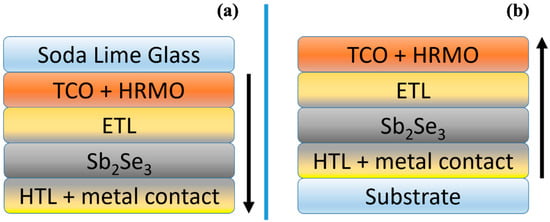
Figure 4.
(a) Schematic representation of the superstrate and (b) substrate solar cell; the arrows point out the deposition sequence.
The substrate configuration means that layers are deposited starting from the back contact, typically molybdenum. Even though a simple contact between ASe and Mo leads to the formation of a contact barrier, this problem is easily solved by inducing the formation of thin layer of MoSe2, which is a degenerate p-type semiconductor and as such a natural intermediate layer for these cells, similarly to what happens in CIGS-based solar cells [131]. MoSe2 could be formed by direct selenization of the Mo layer [59] or after the deposition of Sb2Se3 through thermal annealing [112,122,132]. There is also another strategy, although less reported in the literature, that consists of thermal annealing of the Mo layer in air to obtain a thin layer of MoO2 that achieves similar results in lowering the contact barrier with ASe [133].
The p-type absorber layer is then deposited, followed by the deposition of the n-type electron transport layer (ETL), which is sometimes referred to as the buffer or window layer from the field of CIGS and Kesterite-based solar cells. Finally, the device is completed by the front contact, which includes a transparent electrode (TE), which may be preceded by a highly resistive layer. Light enters from the top TE; therefore, in this configuration, it is possible to use opaque and/or flexible substrates.
The superstrate configuration means that layers are deposited on a transparent substrate (typically soda-lime glass) starting from the front contact, which is followed by the ETL. Subsequently, the absorber layer is deposited, and finally, the back contact completes the device, which can include a hole transporting layer (HTL), e.g., Spiro-OMeTAD [134] or P3HT [135]. Alternatively, a highly conductive layer such as Fe-S-O [70], NiOx [136] and WO3−x [68] can be used. In this configuration, the light is incoming from the substrate; consequently, only highly transparent substrates can be used. In the case of Sb2Se3, devices are usually built in a superstrate configuration, but record efficiencies have been achieved both in superstrate and substrate configurations with a PCE of 10.57% and 10.12%, respectively [50,60].
Looking at the structure of a superstrate solar cell (see Figure 4a), we first find the front contact. Transparent Conductive Oxides (TCOs), such as ITO (Indium Tin Oxide), FTO (Fluorine-doped Tin Oxide) and AZO (Aluminum-doped Zinc Oxide), are usually used as TE in the field of Sb2Se3 solar cells. Often, an intrinsic Highly Resistive Metal Oxide layer (HRMO) is used as part of a successful ETL/TE combination in order to reduce the shunting paths between the absorber and the TE layers through the thin ETL that could be consumed during the deposition of Sb2Se3 [137]. For example, an intrinsic layer of ZnO has been used successfully in combination with CdS [60,96]. Also, an interfacial layer of SnO2 has been reported to improve the efficiency considerably, although it is quite conductive as an HRMO [138]. Special care should be taken in the choice of the HRMO, since they can induce a variation in the preferential orientation of the absorber or create a high density of acceptor states at the interface with the ETL that leads to the formation of an electron barrier, as is the case of TiO2 [139]. Notwithstanding those important results, high efficiencies were reached even without a highly resistive layer [50,133].
The workhorse material paired as ETL to Sb2Se3 is CdS. CdS was a natural starting candidate as an ETL since it has very favorable properties such as proper bandgap (2.42 eV [140]), conductivity (10−4 Ω−1cm−1 [141]) and carrier mobility (≈102 cm2 V−1 s−1 [58]). CdS had an impressive head start, since it was already successfully employed as an ETL in established technologies such as CdTe and CIGS solar cells; thus, this material is already well characterized [142,143]. A natural band alignment with ASe has made CdS its preferred choice as the n-type partner with a smaller than 0.1 eV conduction band offset, which is sometimes reported as spike-like and sometimes reported as cliff-like [144,145]. Moreover, a better band alignment can be achieved by tuning the band structure by adding Zn [145] or Al [132] to CdS in order to change the band alignment from cliff-like to spike-like with both CdxZn1−xS and CdS:Al being reported to improve the PCE of ASe solar cells.
Although the use of CdS has led to many achievements in terms of performance and durability, there is a constant effort to substitute it with another material for three main reasons. Firstly, even though its use is limited to a very thin layer, CdS remain a highly toxic material, and secondly, because of its energy gap, CdS captures a non-negligible fraction of the solar radiation and as such, this limits the short circuit current (Jsc), so a more transparent ETL could improve the maximum achievable PCE. Lastly, interfacial states between CdS and ASe have been reported and are believed to introduce defects in the active layer [124]. Wide-bandgap compounds have been used as an alternative to conventional CdS, such as TiO2 [115,146,147], SnO2 [148,149], ZnO [74] and Zn1−xMgxO [150], but the PCE of these devices is far lower than the top CdS-based solar cells, as can be seen in Table 2.
Table 2.
Photovoltaic parameters of the best-performing solar cells grown on ETL different from CdS.
As discussed, despite a lot of progress, no crucial step forward has yet been achieved, which is probably because the quality of the bulk layer of Sb2Se3 is at least as important as the interface with the ETL. The presence of deep defects and orientation control must be improved to obtain a higher quality of the absorber material. As discussed above, the VSe acts as a deep defect [107], and efforts are being made to reduce the high-density of VSe in ASe by means of a post-deposition selenization step [56]. By depositing Sb2Se3 with magnetron sputtering, followed by a selenization treatment, an efficiency of 6.06% was achieved with a Voc of 494 mV [111]. The selenization temperature was found to be crucial to effectively passivate the deep defects of the films. Another study, again from sputtered ASe, obtained a high Voc of 504 mV by selenizing a pre-sputtered Sb metallic precursor under Se vapor. The high Voc was attributed to the reduced deep level defect density, the passivated interfacial defects at the heterojunction interface and the treatment-induced Cd and S inter-diffusion [121]. Post-treatment selenization has also been tried on Se-poor Sb2Se3 deposited by VTD in substrate configuration, achieving an impressive Voc of 513 mV and a PCE of 7.4%, which is more than triple the original PCE of 2.41% of the control device [113].
4. Charge Transport, Recombination and Collection
The maximum efficiency reached by a Sb2(Se,S)3-based solar cell, 10.7%, turns out to be very far from the efficiency calculated in the Schockley–Queisser limit (S-Q). In fact, by considering a Sb2(Se,S)3-based solar cell in which the absorber layer has an energy gap of about 1.5 eV, theoretical calculations show the following values of the photovoltaic parameters: Voc = 1.24 V, Jsc = 28.3 mA cm−2, FF = 90% exhibiting a PCE of about 31.5% [124].
The PV parameters shown by the 10.7% efficiency solar cell are: Voc = 0.673 V, Jsc = 23.7 mA cm−2, and FF = 66.8% [51]. These parameters point out that the photocurrent is sufficiently well aligned with the S-Q limit, but the photovoltage and fill factor are very far from their respective calculated values.
The photovoltage deficit (PD) can be evaluated as: PD = Eg/q − Voc, where Eg is the energy gap and q is the elementary charge. By using Sb2Se3 as an absorber layer, with an energy gap of 1.17 eV, solar cells with an average Voc of 0.4 V are routinely obtained. In this case, a PD of about 0.7 V is estimated, which is very high compared to an assessed PD of 0.35 V for CIGS-based solar cells (Eg = 1.08 eV, Voc = 0.735 V) [124].
To reach photovoltages foreseen by the SQ limit, it is necessary to eliminate all sources of Voc-loss. The causes of these losses are to be found in defects generating deep levels in the energy gap, which is responsible for the trapping of charge carriers, or in interfacial defects caused by dangling bonds, lattice mismatches or non-perfect energy band alignment, promoting energy levels which act as recombination centers [119].
Furthermore, since Voc is closely linked to the difference between the quasi-Fermi levels (Fn-Fp), it is important that the materials constituting the p-n junction have a correct doping level for maximizing the (Fn-Fp) difference and consequently the photovoltage.
4.1. Defects Mitigation
As discussed, a large body of research has identified numerous defects, many of which have been correlated with stoichiometric deviations which depend on the growth conditions and therefore on the deposition techniques.
Given the large variety of defects that can contribute to charge trapping and consequently have a large impact on PV performance, manufacturers of Sb2Se3-based solar cells have tried to reduce the number of stoichiometry-related defects as much as possible. For this purpose, post-deposition treatments have been introduced such as annealing in a controlled atmosphere of Se, S (selenization, sulfurization) or reactive treatments with CdCl2, ZnCl2, MgCl2 and SbCl3. As seen above, the main defects in Sb2Se3 are SbSe, VSe, deep or shallow donors, and SeSb antisites if the deposition environment is in Se-poor or Se-rich conditions, respectively.
All these attempts have led to slight improvements in cell performance, but none have shown a clear path forward regarding deposition techniques and/or post-deposition treatment.
A second strategy to make defects less problematic is to extrinsically dope the p-type Sb2Se3 film. First-principle calculations showed different behavior for metal or non-metal dopants. SnSb and ZnSb generate acceptor levels that increase the p-type conductivity, while TiSb and PbSb act as donor defects [151], giving rise to compensation effects with a consequent decrease in the p-type conductivity. Among metal dopants, copper deserves a separate discussion because when it substitutes antimony, it increases the p-type conductivity by increasing the density of the active acceptor levels at room temperature [152]. At the same time, the presence of copper enhances the crystalline quality of the Sb2Se3 films, and it also improves the average size of the crystalline grains and the vertical orientation of the ribbons. On the other hand, interstitial copper (Cui) contributes with a donor level. This is typically the most likely situation, occurring at the grain boundaries and on the surface of the Sb2Se3 film. The n-type surface of grain boundaries favors the collection of minority carriers acting as fast transport channels for the photogenerated electrons. Because of the lack of one type of charge carrier, the non-radiative recombination inside the crystalline grain is substantially reduced. To achieve good ohmic contact with the HTL, the surface of the film with the population inversion is cleaned by chemical etching with ammonium sulfide [152].
Among the heat treatments in the presence of non-metallic elements, the one with chlorine is effective in n-type doping. In fact, ClSb generates a shallow donor level, giving rise to the formation of intriguing isotype n-n heterojunctions [153]. On the contrary, by increasing the Cl concentration, compensating deep levels appear due to the presence of Cli, voiding any doping effect eventually introduced.
Doping with Te is effective in modifying the Sb/Se ratio since Te prefers to form Sb2Te3 rather than Sb2(Se,Te)3, favoring the reduction in the VSe vacancies and consequently implementing the p-type conductivity [116].
Conversely, doping with alkali metals such as Na and K creates Se vacancies, making Sb2Se3 films more n-type doped. The heavier alkali metals having large ionic radii have difficulty entering the Sb2Se3 crystal lattice with difficulty and do not behave as effective dopants. Moreover, they are very effective in increasing crystallinity; in fact, Sb2Se3 films treated with Rb and Cs have large crystalline grains with an evident vertical preferential orientation [154].
However, most of the research is focused on diminishing the intrinsic defects that are native during the growth of Sb2Se3 (Sb2S3) films, often using post-deposition treatments. One of these consists in passivating the Se vacancies using a suitable partial pressure of oxygen during the deposition of the Sb2Se3 (Sb2S3) films or by applying post-deposition treatments in the presence of O2 [155]. Theoretical simulations show that due to the lower enthalpy of formation (Hf) of OSe and OS compared to VSe and VS, oxygen can effectively passivate both selenium and sulfur vacancies [156].
4.2. Reducing Recombination Losses
To explain how recombination losses and photovoltage deficit are correlated, the behavior of Voc as a function of T was extensively studied. The starting point could be the following relationship [157]:
where q is the electron charge, Ea is the activation energy of the recombination center, A is the ideality diode factor, k is the Boltzmann constant, T is the absolute temperature, J00 is the reference current density of the thermal activated current density J0 and Jsc is the photocurrent. If J0 and A are weakly temperature-dependent or completely independent from the temperature, a plot of Voc as a function of T allows obtaining the activation energy Ea in approaching the zero limit of T. According to [158], if Ea is much smaller than the energy gap Eg of the absorber, the main loss mechanism is the interface recombination, which can occur both at the junction (ETL/Sb2Se3) or at the back-contact (Sb2Se3/HTL). Conversely, if Ea is nearly equal to Eg, the main recombination process is the Shockley–Read–Hall (SRH) recombination in the space charge region (SCR) and in the neutral region toward the back contact.
Often, it is observed that Ea for Sb2Se3-based solar cells is smaller than Eg, suggesting that the major cause for the Voc loss is interface recombination mainly due to lattice mismatch, non-perfect alignment of the energy bands and a possible contact barrier.
The Sb2Se3 film grows with different preferential orientations, depending on the substrate material [71] and on the deposition technique used. The crystalline quality and the preferential orientation strongly influence the presence and number of defects that can behave as recombination centers. Concerning this, it is often observed that the [221] preferred orientation of the Sb2Se3 layer is effective in reducing recombination at the Sb2Se3/ETL interface [74]. The parameter that provides an estimate of the contribution of crystallographic orientations of the Sb2Se3 film is the texture coefficient (TC), which is generally defined as [159]:
where N is the number of XRD peaks considered while Ihkl and I0hkl are the intensity of the peak related to (hkl) planes for the experimental and powder sample, respectively. By definition, TChkl is always comprised between 0 and N. When TChkl is greater than one, then the grains in the film are preferentially oriented along the (hkl) directions.
The TC value has a great influence on the PV parameters both for substrate and superstrate configuration, and indeed, correlations between TChk0 [57] and TChk1 [160] and the PV parameters of the device were experimentally observed.
As can be seen in Table 3, both superstrate and substrate Sb2Se3 solar cells with good PV parameters have preferential orientation along the directions (221), (211) and (002). Those are the situations in which the (Sb4Se6)n chains are perpendicular to the substrate and charge transport is enhanced, since the carriers can flow through the covalent bonds that run along the chains. The presence of dangling bonds at the end of the chains is also responsible for a better matching between the ETL and the absorber at the interface, and this is probably why less recombination defects are accompanied by increased preferential direction along (221), (211) and (002) [147]. A better optimization of deposition conditions can tune the preferential orientation of Sb2Se3 films, but the choice of the substrate has proven to be crucial [71].
Table 3.
Photovoltaic parameters of solar cells in substrate and superstrate configuration. Deposition techniques: Radio Frequency Magnetron Sputtering (RFMS), Close-Spaced Sublimation (CSS), Vapor Transport Deposition (VTD), Coevaporation (CoE), Injection Vapor Deposition (IVD).
Another demonstration that the substrate on which antimony chalcogenides are deposited plays a fundamental role is represented by a Sb2S3 layer deposited on TiO2 films by rapid thermal evaporation (RTE), showing a quasi-epitaxial growth characterized by (hk1) preferential orientation. Solar cells created with these films exhibited a low density of recombination centers at the TiO2/Sb2S3 interface with an enhanced Voc of 0.69 V [164]. This could pave the way for a quasi-epitaxial growth of Sb2X3 (X = S, Se) films to obtain high-quality heterointerfaces.
As stated above, point defects generate a lot of deep levels into the Sb2Se3 energy gap and, excluding the ones with an amphoteric behavior [109], among the others, VSe2, VSe3, SbSe2 and SeSb1, having a low formation energy, are easily formed and create deep levels that act as recombination centers. A unique strategy to mitigate the effect of these punctual defects at the same time is very hard to develop, since the first three are easily avoided in Se-rich conditions, and the fourth is prevented in Se-poor conditions. These deep levels contribute to the pinning of the Fermi level, heavily affecting the photovoltage deficit.
Investigating the deep levels in VTD-deposited Sb2Se3 films by the deep-level transient spectroscopy (DLTS) technique, Wen et al. [61] found three defects localized at Ec −0.61 eV, Ev + 0.71 eV and Ev + 0.48 eV. The first one behaves like an electron-traps defect, while the other two are hole-traps defects, as already reported above in Section 2.3. In [61], the authors hypothesized that these deep energy levels are due to antisite defects, i.e., SbSe, SeSb and VSb, respectively. Ma et al. found in [116] only two deep levels in Te-doped Sb2Se3, attributing them to the same antisite defects, namely: SbSe and SeSb. These defect pairs probably form a highly localized complex (SbSe + SeSb) [124], giving rise to non-radiative recombination centers, which strongly influence the performance of the solar cell, in particular the Voc deficit.
More generally, all the defects related to impurities, a low level of crystallinity and disorder generate band tail states. The band tail states could reduce the energy gap with an immediate negative effect on Voc. Moreover, the charge carriers are localized into these states, which act as traps, causing the deterioration of all the photovoltaic parameters of the solar cells. In Table S2 of the supplementary information from [124], Urbach energies E0 are reported, which indicates how large the band tails are in Sb2Se3 deposited with different techniques. Amorphous antimony selenide exhibits very large values, up to E0 = 200 meV, while the polycrystalline material shows E0 values of about 30–40 meV. These values can be compared with the those of polycrystalline thin film solar cells: CIS (E0 ≈ 27 meV), CdTe (E0 ≈ 15 meV) and Pb-based perovskite (E0 ≈ 15 meV). From this comparison, it is evident that a large part of the photovoltage loss in antimony chalcogenide material is due to the high value of E0. However, it remains established that in optimized deposition, the Sb2Se3 film grows with well-oriented grains in the [001] direction; this growth minimizes defects due to grain boundaries; hence, the large E0 value is almost entirely due to interface and bulk defects. For these reasons, it is crucial to understand the role of ETL/Sb2Se3 and HTL/Sb2Se3 interfaces and their associated band alignment.
It is always difficult to find a good ohmic contact with p-type semiconductors that give low resistance and proper alignment of the energy bands. This is because such semiconductors exhibit high electron affinity values. There are few materials that have the right characteristics to make a good contact with p-Sb2Se3. For example, metals with a high work function (Pt, Au, Pd) can form a good band alignment; however, metals can also diffuse into the grain boundaries of polycrystalline films, undermining the overtime stability of the devices. Moreover, the alignment of the energy bands and time stability are not the only characteristics to be taken into consideration but also the non-toxicity and abundance of the constituent elements, ease of end-of-life recycling, the low cost and the simplicity of the preparation process are some of the main requirements needed for a good hole transport material (HTM). A lot of attempts were made by using PbS quantum dots [58], CuSCN [165], PEDOT [166], spiro-OMeTAD [167] and FeSO [70] as HTMs, but none of these attempts seemed definitive, and there is still a long way to go to find a fully satisfactory contact. In fact, very frequently, the surface of antimony selenide polycrystalline films is slightly oxidized due to some passage in air, or there are unsaturated bonds due to Sb-rich conditions. HTMs such as PbS quantum dots, poly(3-hexylthiophene-2,5-diyl) (P3HT) [168], poy(3,4-ethylenedioxythiophene) polystyrene sulfonate (PEDOT:PSS) and FeSO represent a good choice, since the presence of sulfur ensures the passivation of defects on the surface of Sb2Se3 by replacing the oxygen atoms or by binding to antimony.
Concerning electron transport materials (ETMs), the most frequently used is certainly CdS, although it presents some drawbacks like high lattice mismatch and the diffusion of Cd ions inside the Sb2Se3 film. The difference in the lattice constants can be minimized, favoring the formation of a mixed layer, similarly to what happens in the CdTe-based solar cell [169]. For the Sb2Se3/CdS system, the formation of a mixed layer is very critical since the two materials are not homologous, like CdS and CdTe, but at the same time, the diffusion of single Cd atoms into the Sb2Se3 film must be avoided to prevent the formation of deep traps. Also in this case, a lot of attempts were made; all of which were focused on the optimization of band alignment and suppression of the lattice mismatch to minimize the interface states [112,132,147,162,170].
In addition to these considerations, correct band alignment is always important to avoid recombination at the ETM/Sb2Se3 interface, which can be very detrimental to the photovoltage. In [171], the authors well described the behavior of different ETMs, such as CdS, ZnO and TiO2, when coupled with Sb2Se3. It was experimentally observed, in good agreement with thermodynamic considerations, that the interface reaction between Sb2Se3 and these ETMs is higher for CdS, followed by ZnO and TiO2 in this order. Therefore, different intermixing transition materials at the interface with Sb2Se3 are formed. These transition layers are responsible for a suppression or an increase in the number of the recombination centers at the interface with a heavy consequence on the photovoltage deficit. In the same study, the conduction band offsets (CBO) between Sb2Se3 and CdS, ZnO and TiO2, starting from high-resolution photoemission spectroscopy (HRPES) data, were also calculated, finding the following behavior: a conduction band offset of 0.24 eV of the Sb2Se3/CdS heterointerface shows a peak-like band alignment; the −0.11 eV CBO of the Sb2Se3/ZnO system shows a cliff-like band alignment, while with TiO2, the band alignment is rather flat. Cliff-like CBO enhances recombination at the interface, while moderate spike-like CBO helps in recombination suppression, charge separation, and charge collection.
For this reason, many Sb2Se3-based devices have CdS as ETM, which generally gives good PV parameters of the solar cells.
Several attempts have been made to improve the band alignment between ETMs and Sb2Se3 and to find suitable treatments to remove the surface defects for the suppression of the recombination centers. TiO2 [167], CeO2 [172], ZnCdS [145], In2S3 [173], CdSe [174] and CdS:O [175] are only some of the Sb2Se3 partners studied to optimize energy band alignment through interface engineering. Moreover, to reduce interface defects, the surface of TiO2 [176] and In2S3 [177] films were treated with zinc halides. These attempts demonstrate that there is still much work to be completed to address the remaining knowledge gaps and to introduce successful strategies to minimize defect density in Sb2Se3 films, both in the bulk and at the interface with HTM and ETM. Even further, great importance must be given to the optimization of band alignment between the absorber and charge transport layers.
5. Deposition Techniques
As stated above, the preparation of high-quality Sb2Se3 thin films with low defect density is needed to diminish the recombination of photogenerated electron–hole pairs and for reducing the performance losses of the photovoltaic devices. This aspect becomes particularly important in the deposition of the absorber film on top of the ETL material (CdS, ZnCdS, ZnO, TiO2, ZnS, Zn(S,O), MgZnO, ZnSe). The pseudo-1D structure of Sb2Se3 films offers the possibility of an efficient charge transport along ribbons, where recombination is sufficiently low. The deposition techniques must therefore consider the anisotropic growth of the Sb2Se3, favoring the crystallization of the films with the ribbons oriented in the correct direction with respect to the transport of the photogenerated charge carriers. In recent times, the deposition of Sb2Se3 thin films has been carried out by physical and/or chemical techniques. In the following, we briefly list the main techniques which achieved devices with conversion efficiencies of 2%.
Physical techniques include the following.
1. Electron-Beam Gun (EBG)
This high-vacuum deposition technique consists of a crucible kept cold by a coolant, bombarded by an energetic electron beam, and driven by an electromagnetic lens. By controlling the energy and intensity of the electron beam, the deposition rate of the film can be tuned. If the deposition system is equipped with a rotating heating substrate holder, excellent thickness and stoichiometric uniformity is guaranteed. The Sb2Se3 deposition can take place by heating the substrate up to a maximum temperature of Ts = 300 °C, above which the material begins to re-evaporate. Films deposited with this technique, at temperatures Ts ≤ 300 °C, show Sb-rich stoichiometries, although the bombardment with a beam of energetic electrons helps to keep the Sb2Se3 starting stoichiometry. For this reason, thermal treatments in a Se-controlled atmosphere of the EBG-deposited Sb2Se3 film are necessary. With this technique, Sb2Se3-based solar cells realized in substrate configuration (SLG/Mo/ Sb2Se3/CdS/ZnO) by using (hk0) oriented films show PCE just above 4% [178].
2. Thermal Evaporation (TE)
By placing the material to be evaporated/sublimated in a crucible, which can be heated directly by the Joule effect or indirectly with IR lamps, it is possible to change the deposition rate by controlling the heating temperature of the container. This technique, similarly to EBG high-vacuum deposition, obtains Sb2Se3 thin films with the correct morphology and crystalline structure. Since the deposition is carried out under high-vacuum condition, the temperature of the depositing film cannot exceed 300 °C, as in the previous case. The crucible is kept at a high temperature; thus, no chemical interaction with the material inside is strictly required. For this purpose, inert materials such as alumina, graphite, quartz, or refractory metals such as tungsten, molybdenum and tantalum are used. With this very versatile technique, Sb2Se3, Sb2S3 or a mixture of the two, depending on the starting material placed inside the crucible, can be deposited [179]. Solar cells, fabricated in a superstrate configuration with CdS/Sb2SxSe3−x, (x = 1.05) as active layers showed a PCE in the range 5–6%. With the TE technique, solar cells were also made in substrate configuration (Ag/ITO/ZnO/CdS/Sb2Se3/Mo/glass) exhibiting PCE of around 4.2% [69].
3. Vapor Transport Deposition (VTD)
A vapor transport process for the deposition of a compound in the form of a thin film consists of a saturated carrier gas with a vapor coming from the compound source. The saturated mixture is directed over a substrate kept at lower temperature than that of the source, resulting in a locally supersaturation condition and subsequent film growth. Contrary to what happens in the rapid thermal evaporation process (RTE), where the crucible substrate is very close with a fixed distance, in the VTD technique, both the substrate temperature and the distance between the source and substrate are changeable, allowing a better control of the atomic species in the vapor phase, which favors the growth of a highly oriented Sb2Se3 film with improved crystallinity and reduction in defects. Sb2Se3 films, VTD-deposited, realized for the first time a superstrate solar cell (ITO/CdS/Sb2Se3/Au) showing a PCE of 7.6% [61].
The good miscibility of Sb2Se3 and Sb2S3, having both orthorhombic crystal structures (Pnma 62), is exploited to obtain different Sb2(Se,S)3 materials characterized by a continuously tunable bandgap from 1.1 to 1.7 eV by changing the Se/S ratio. By applying different mixed powders of Sb2Se3 and Sb2S3 as evaporation sources in a VTD process, Sb2(S,Se)3 films with different Se/S ratio are obtained. An optimized device (Glass/ITO/CdS/Sb2(S,Se)3/Au) based on this material showed a PCE of 7.1% [180]. With a modified dual-sources VTD system, one for sulfide and one for selenide, a Sb2(S,Se)3 alloyed film, showing superior crystalline quality, was realized. By using this Sb2(S,Se)3 thin film, a glass/ITO/CdS/Sb2(S,Se)3/Au superstrate device achieved a PCE of 8.17%, which is the highest value among antimony chalcogenide-based solar cells manufactured via the dual-source VTD system [181].
4. Close-Spaced Sublimation (CSS)
In Close-Spaced Sublimation (CSS), Sb2Se3 is sublimated from a solid source in the form of granules or of a compact material obtained by melting the Sb2Se3 in powder under an inert gas pressure. The deposition of Sb2Se3 films by the CSS method is based on the reversible dissociation of Sb2Se3 at high temperature in an inert gas environment at a pressure between 1 and 100 Pa. The Sb2Se3 source dissociates into its elements, which recombine on the substrate surface, depositing a polycrystalline film. From this point of view, CSS and VTD are very similar techniques; the only difference is that in CSS, the deposition takes place in a static atmosphere, while VTD are supported by a flow of the carrier gas. Therefore, the CSS is typically characterized by a vertical deposition, while in VTD, the deposition is horizontally performed, following the gas flow direction. In CSS, the sublimation rate strongly depends on the temperature of the source and the pressure of the inert gas in the reaction tube; consequently, the deposition rate of Sb2Se3 increases exponentially with the source temperature and decreases with chamber pressure. Sb2Se3 nanorods CSS-deposited on Mo-covered soda-lime glass were used to produce solar cells in substrate configuration (Mo/MoSe2/Sb2Se3/CdS/i-ZnO/Al:ZnO/Ag), which exhibits the remarkable efficiency of 9.2% [59]. After a lot of different attempts made for optimizing the CSS deposition parameters, the window material on which Sb2Se3 grows, the interface between the two materials, and the back-contact, an efficiency in the range 6–7.29% was reached with solar cells realized in superstrate configuration [175,182,183].
5. Sputtering (SP)
Sputtering (SP) deposition consists of exploiting the energy confined in a plasma (ionized gas) on the surface of a target, to drag the atoms of the constituent material one by one and deposit them on a substrate. Plasma is generated by the ionization of a pure inert gas, usually argon, by an electric potential difference (pulsed DC) or by an electromagnetic excitation (MF, RF); the Ar+ ions are accelerated by the electric field and confined to the surface of the target due to the presence of a magnetic field. Each Ar+ ion, hitting the surface target, transfers its energy and momentum to tear off atoms, which have enough energy to be projected onto the substrate. The typical SP deposition parameters are power density, deposition rate, working Ar pressure, substrate temperature, target stoichiometry, and target–substrate distance. SP is considered one of the most suitable techniques to transfer the manufacture process of the solar cell from laboratory scale to the industrial production of photovoltaic modules. Between solar cells realized in substrate architecture, it is worth of mentioning the selenization of Sb elemental layers deposited by SP. By optimizing the selenization of the Sb precursors, solar cells in substrate configuration (Mo/Sb2Se3/CdS/ITO/Ag) with a high fill factor (FF) of about 59.3% and an efficiency above 6.11% were obtained [184]. Depositing directly Sb2Se3 film by the SP technique in a substrate configuration solar cell (Mo/Sb2Se3/CdS/ITO/Ag), with a fine tuning of the Ar working pressure during the deposition process and performing an optimized heat treatment in a controlled Se atmosphere, led to an interesting PCE of 5.52% [185].
The efficiency record for substrate solar cells in which the Sb2Se3 layer was deposited by sputtering was obtained by improving the post-deposition heat treatment in a controlled SE atmosphere. In fact, by performing rapid thermal annealing, the efficiency of the device passed from 5.37% to a remarkable 8.64% [112]. On the contrary, superstrate solar cells (ITO/CdS/Sb2Se3/Au), involving Sb2Se3 film SP-deposited, exhibit quite low PCE around 2–2.5%, showing a net difficulty in obtaining higher efficiency, which is probably due to a strong interaction between the window and the Sb2Se3 films due to the high energy of the impinging Sb, Se and SbxSey atoms and molecules, which is typical of the SP technique [186].
6. Pulsed Laser Deposition (PLD)
Pulsed Laser Deposition (PLD) is a thin film deposition technique that uses high-energy laser pulses to evaporate/sublimate the surface of a material inside a vacuum chamber and condenses the vapor onto a substrate to form a thin film few micrometers thick. The main advantages of this technique follow: (i) the possibility of producing a film with the same composition of the starting material, which forms the target and (ii) many materials can be deposited in different gas atmospheres over a wide range of gas pressures. By exploiting the stoichiometric deposition typical of this technique, with the possibility of performing the deposition at high temperature, solar cells in superstrate configuration were realized by depositing both the active layers, CdS and Sb2Se3. In particular, by depositing the Sb2Se3 layer at a temperature of 500 °C, superstrate solar cells (FTO/SnO2/CdS/Sb2Se3/Au) exhibiting a PCE of about 4.4% were obtained [187].
A very similar deposition technique is the so-called Pulsed Electron Deposition (PED), in which the laser beam is substituted by a high-power electron beam in the PLD deposition system. PED is particularly useful for depositing films stoichiometrically equivalent to the material constituting the target, even considering low deposition temperatures, such as 200 °C. With this technique, an interesting bifacial solar cell showing a PCE of about 3% was realized [72].
Chemical techniques include the following.
1. Spin Coating (SC)
The spin-coating technique (SC) is used to prepare uniform thin films in the micrometer to nanometer thickness range. The substrate is mounted on a mandrel which rotates the sample and centrifugal force pushes the liquid solution, containing the material to be deposited, radially outward. Viscous force and surface tension, which define the wettability of the substrate surface, are the main causes of flat deposition. Finally, the thin film is formed by evaporation of the solvents contained in the solution used for the deposition.
The FTO/CdS/Sb2Se3/Spiro-OMeTAD/Au superstrate solar cells, realized with spin-coated Sb2Se3 film doped with Te, exhibited a PCE around 5.5%, which is a remarkable efficiency for a solution-processed solar cell [188]. Moreover, by using TiO2 and Spiro-OMeTAD as electron and hole transport layers, respectively, an FTO/TiO2/Sb1.9S2.2Se0.9/Spiro-OMeTAD/Au superstrate solar cell was realized by using a spin-coated Sb2S3−xSex mixed compound, obtaining a PCE of 5.8% [116].
2. Hydrothermal Synthesis (HyS)
Hydrothermal synthesis (HyS) or the hydrothermal method is defined as a single crystal synthesis method depending on the solubility of the materials to be grown in hot water under high pressure. Crystal growth is carried out in an autoclave, in which a nutrient is supplied together with water. Maintaining a temperature gradient at the ends of the growth chamber, this causes the material deposition onto a crystal seed, growing the desired crystal at the cooler end, while at the hotter end, the material dissolves in the under-pressure water vapor. If there is no crystal seed on which to grow the material, but on the contrary, there is an amorphous substrate such as soda-lime glass, a polycrystalline film will be deposited. There are a lot of articles in the literature which report on solar cells realized with Sb2(S,Se)3 HyS-deposited film. Here, we only mention an FTO/Zn(O,S)/CdS/Sb2(S,Se)3/Spiro-OMeTAD/Au superstrate solar cell realized with a Sb2(S,Se)3 film HyS-deposited on top of the CdS layer showing a PCE of 10.7%, which is the higher value so far obtained with antimony chalcogenides as the absorber material [51].
3. Chemical Bath Deposition (CBD)
The CBD process exploits the reaction between a metal ion source, a chalcogenide source and a base in a solution to produce a precipitate that is deposited onto a substrate. Special additives can be used to slow down or speed up the reaction kinetic. This technique has become widely used for depositing metal chalcogenides semiconductors mainly because of its simplicity and reproducibility [189,190].
CBD could be considered the simplest technique in this panel, as it has the minimum requirements to meet, namely: a container for the solution, the substrate and the chemical precursors. Usually, a stirring mechanism, a thermostat bath and a pH meter are also present to better control the reactions. The lack of complicated sensors and of vacuum apparatus as well as low process temperature are the main advantages of this technology that makes it particularly cost-effective for depositing thin film over large areas. The cons are that the as-prepared films are mostly amorphous; thus, post-heat treatment is required to crystallize the layer [54,94,191]. Moreover, additives need special attention to avoid impurities in the resulting films [192]. Furthermore, the residual products are considered special waste, and their disposal constitute an additional source of cost and concerns.
The idea of depositing A2B3 materials as absorbing films for solar cells using CBD dates to 1997 [76], but it was only in 2009 that a real working device was reported [54]. CBD was particularly successful for Sb2S3-based solar cells, achieving efficiencies as high as 7.5% in 2014 [52], and it was the natural starting candidate for growing antimony selenide as well. Indeed, CBD was the first technique used to deposit antimony selenide as an absorber material for solar cells [54], but after this first success, most of the research turned into vacuum techniques, which gained popularity after achieving a record PCE of 3.14% in 2015 [56]. While vacuum techniques have guided most of the improvements in the field until now, CBD remained in the background and was mostly used for the deposition of CdS as ETL. Recently, CBD has regained attention after the work of Zhao et al., which achieved a record PCE of 9.17% and 10.57% using thiourea and selenourea, respectively, as additives to precisely regulate the reaction process [50].
6. Conclusions
We have reviewed recent advances in the performance of Sb2Se3-based solar cells with a focus on material properties as a function of deposition techniques and growth parameters. Many articles have been published on Sb2Se3 and related compounds, which is a clear sign of the growing interest in this material.
Within a few years, the barrier of 10% photovoltaic conversion efficiency has been overcome, and many hopes are pinned on the development of solar cells based on these chalcogenides, both for their high sustainability and for the excellent chemical–physical properties, which make these materials ideal candidates for large-scale photovoltaic development.
Sb2Se3 is a material that is particularly sensitive to stoichiometric defects, the quality of the interface with the ETL (n-type partner) with which it forms the junction, and how the ribbons are oriented within the crystalline grains. All these sources of defects contribute to the introduction of energy levels into the forbidden gap, increasing the possibility of recombination and trapping of charge carriers. In the future, research will go in the direction of minimizing these defects in order to increase photovoltaic conversion efficiency.
Voc and FF will obtain an improvement through an optimized management of the charge transport and the charge carrier recombination mechanisms, which is a result obtainable by controlling the structural defects. Deep levels in the energy gap, introduced by surface, interface or bulk defects, handle the low Voc value due to the pinning of the Fermi level. This task, while difficult to achieve, is becoming increasingly necessary if the bottleneck of improving PV conversion efficiencies is to be overcome.
For the improvement of the PCE, we cannot exclude the optimization of the electron transport layer to increase the transparency and consequently the photogenerated current.
From this point of view, we can draw on the research conducted on CdTe and CIGS in which materials such as ZnO, ZnS, ZnSe and MgZnO, useful for increasing transparency at short wavelengths of the visible spectrum, have been used. Furthermore, these materials are more sustainable than the more common CdS aiming for a cadmium-free device. It seems also reasonable that Cd diffusion inside Sb2Se3 is the origin of defects, which leads to an unwelcome instability over time. Lastly, the interface with the back contact should not be overlooked: in addition to creating ohmic contact, it must guarantee stability over time, avoiding a possible diffusion of the metals constituting the contact itself into the absorber material.
Summarizing, the salient topics on which the future research is necessary for finding new solutions follow:
- The selection of appropriate n-type materials to couple with Sb2Se3 is vital to reduce interface recombination and to increase the diode rectification and the shunt resistance. Furthermore, rising the transparency of the n part of the p-n junction will be beneficial in increasing the photocurrent;
- The control of the orientation of the Sb2Se3 film is of fundamental importance for this material due to the particular 1D crystalline structure;
- The deposition technique can also play a fundamental role, since performing the deposition in a Se-rich or Se-poor atmosphere means having control over the substitutional defects of Sb and Se, respectively, as well as over the interstitial defects which, as a rule, generate deep harmful levels in the energy gap;
- The engineering of the energy bands, the formation of alloys with Sb2S3, the passivation of interface defects and, more generally, the control of defects will have an increasingly crucial role;
- To overcome this challenge, it is necessary to find an effective way to render the defects that generate deep levels or recombination centers harmless. One possible strategy is to introduce p-type dopants to increase the intrinsic low carrier density of Sb2Se3.
With additional exploration on the listed aspects, the efficiency of the Sb2Se3-based solar cells will be improved to develop a highly sustainable technology suitable for TW production, which is increasingly needed to minimize the greenhouse effect and to favorably influence climate change.
Author Contributions
A.B., G.F., S.P. and D.S. wrote the original draft of this manuscript; A.B. and D.S. revised and confirmed the manuscript, A.B. offered financial support. All authors have read and agreed to the published version of the manuscript.
Funding
This research was funded by National Recovery and Resilience Plan (NRRP), Mission 4 Component 2 Investment 1.5—Call for tender No. 3277 of 30/12/2021 of Italian Ministry of University and Research funded by the European Union—NextGenerationEU. Award Number: Project code ECS00000033, Concession Decree No. 1052 of 23/06/2022 adopted by the Italian Ministry of University and Research, CUP D93C22000460001, “Ecosystem for Sustainable Transition in Emilia-Romagna” (Ecosister).
Data Availability Statement
Data will be made available on request.
Conflicts of Interest
The authors declare no conflict of interest.
References
- IEA. World Energy Outlook 2022; IEA: Paris, France, 2022. [Google Scholar]
- Ramanujam, J.; Verma, A.; González-Díaz, B.; Guerrero-Lemus, R.; del Cañizo, C.; García-Tabarés, E.; Rey-Stolle, I.; Granek, F.; Korte, L.; Tucci, M.; et al. Inorganic Photovoltaics—Planar and Nanostructured Devices. Prog. Mater. Sci. 2016, 82, 294–404. [Google Scholar] [CrossRef]
- Grätzel, M. Solar Energy Conversion by Dye-Sensitized Photovoltaic Cells. Inorg. Chem. 2005, 44, 6841–6851. [Google Scholar] [CrossRef] [PubMed]
- Available online: https://www.Nrel.Gov/Pv/Assets/Pdfs/Cell-Pv-Eff-Crysi.Pdf (accessed on 27 August 2023).
- Polverini, D.; Field, M.; Dunlop, E.; Zaaiman, W. Polycrystalline Silicon PV Modules Performance and Degradation over 20 Years. Prog. Photovolt. Res. Appl. 2013, 21, 1004–1015. [Google Scholar] [CrossRef]
- Bathey, B.R.; Cretella, M.C. Solar-Grade Silicon. J. Mater. Sci. 1982, 17, 3077–3096. [Google Scholar] [CrossRef]
- Lan, C.-W.; Hsieh, C.-K.; Hsu, W.-C. Czochralski Silicon Crystal Growth for Photovoltaic Applications. In Crystal Growth of Si for Solar Cells; Nakajima, K., Usami, N., Eds.; Springer: Berlin/Heidelberg, Germany, 2009; pp. 25–39. [Google Scholar]
- Li, M.; Dai, Y.; Ma, W.; Yang, B.; Chu, Q. Review of New Technology for Preparing Crystalline Silicon Solar Cell Materials by Metallurgical Method. IOP Conf. Ser. Earth Environ. Sci. 2017, 94, 012016. [Google Scholar] [CrossRef]
- Hull, R. Properties of Crystalline Silicon; IET: Stevenage, UK, 1999; ISBN 0852969333. [Google Scholar]
- Kangsabanik, J.; Svendsen, M.K.; Taghizadeh, A.; Crovetto, A.; Thygesen, K.S. Indirect Band Gap Semiconductors for Thin-Film Photovoltaics: High-Throughput Calculation of Phonon-Assisted Absorption. J. Am. Chem. Soc. 2022, 144, 19872–19883. [Google Scholar] [CrossRef]
- Bube, R.H. Photovoltaic Materials; Newman, R.C., Ed.; Imperial College Press: London, UK, 1998; Volume 1, ISBN 1-86094-065-X. [Google Scholar]
- Stutenbaeumer, U.; Lewetegn, E. Comparison of Minority Carrier Diffusion Length Measurements in Silicon Solar Cells by the Photo-Induced Open-Circuit Voltage Decay (OCVD) with Different Excitation Sources. Renew. Energy 2000, 20, 65–74. [Google Scholar] [CrossRef]
- Alharbi, F.; Bass, J.D.; Salhi, A.; Alyamani, A.; Kim, H.C.; Miller, R.D. Abundant Non-Toxic Materials for Thin Film Solar Cells: Alternative to Conventional Materials. Renew. Energy 2011, 36, 2753–2758. [Google Scholar] [CrossRef]
- Sugaya, T.; Makita, K.; Takeda, A.; Oshima, R.; Matsubara, K.; Okano, Y.; Niki, S. InGaP/GaAs Tandem Solar Cells Fabricated Using Solid-Source Molecular Beam Epitaxy. Jpn. J. Appl. Phys. 2014, 53, 05FV06. [Google Scholar] [CrossRef]
- Miyashita, N.; Okada, Y. Inverted Lattice-Matched GaInP/GaAs/GaInNAsSb Triple-Junction Solar Cells: Epitaxial Lift-off Thin-Film Devices and Potential Space Applications. In Photovoltaics for Space; Elsevier: Amsterdam, The Netherlands, 2023; pp. 265–291. [Google Scholar] [CrossRef]
- Schön, J.; Bissels, G.M.M.W.; Mulder, P.; van Leest, R.H.; Gruginskie, N.; Vlieg, E.; Chojniak, D.; Lackner, D. Improvements in Ultra-light and Flexible Epitaxial Lift-off GaInP/GaAs/GaInAs Solar Cells for Space Applications. Prog. Photovolt. Res. Appl. 2022, 30, 1003–1011. [Google Scholar] [CrossRef]
- Van Rossum, M. Integrated Circuits. In Encyclopedia of Condensed Matter Physics; IMEC: Leuven, Belgium, 2005; pp. 394–403. [Google Scholar] [CrossRef]
- Geisz, J.F.; France, R.M.; Schulte, K.L.; Steiner, M.A.; Norman, A.G.; Guthrey, H.L.; Young, M.R.; Song, T.; Moriarty, T. Six-Junction III–V Solar Cells with 47.1% Conversion Efficiency under 143 Suns Concentration. Nat. Energy 2020, 5, 326–335. [Google Scholar] [CrossRef]
- Papež, N.; Dallaev, R.; Ţălu, Ş.; Kaštyl, J. Overview of the Current State of Gallium Arsenide-Based Solar Cells. Materials 2021, 14, 3075. [Google Scholar] [CrossRef]
- Levillayer, M.; Arnoult, A.; Massiot, I.; Duzellier, S.; Nuns, T.; Inguimbert, C.; Aicardi, C.; Parola, S.; Carrère, H.; Balocchi, A.; et al. As-Grown InGaAsN Subcells for Multijunction Solar Cells by Molecular Beam Epitaxy. IEEE J. Photovolt. 2021, 11, 1271–1277. [Google Scholar] [CrossRef]
- Miglio, L.; Sassella, A. Epitaxy. In Encyclopedia of Condensed Matter Physics; Università degli Studi di Milano: Milan, Italy, 2005; pp. 157–166. [Google Scholar] [CrossRef]
- Massiot, I.; Cattoni, A.; Collin, S. Progress and Prospects for Ultrathin Solar Cells. Nat. Energy 2020, 5, 959–972. [Google Scholar] [CrossRef]
- Abegunde, O.O.; Akinlabi, E.T.; Oladijo, O.P.; Akinlabi, S.; Ude, A.U. Overview of Thin Film Deposition Techniques. AIMS Mater. Sci. 2019, 6, 174–199. [Google Scholar] [CrossRef]
- Depla, D.; Mahieu, S.; Greene, J.E. Sputter Deposition Processes. In Handbook of Deposition Technologies for Films and Coatings; Elsevier: Amsterdam, The Netherlands, 2010; pp. 253–296. [Google Scholar]
- Seshan, K. Handbook of Thin Film Deposition Techniques Principles, Methods, Equipment and Applications, 2nd ed.; CRC Press: Boca Raton, FL, USA, 2002; ISBN 9780429076749. [Google Scholar]
- Romeo, A.; Bätzner, D.L.; Zogg, H.; Tiwari, A.N. Recrystallization in CdTe/CdS. Thin Solid Films 2000, 361–362, 420–425. [Google Scholar] [CrossRef]
- Ferekides, C.; Britt, J.; Ma, Y.; Killian, L. High Efficiency CdTe Solar Cells by Close Spaced Sublimation. In Proceedings of the Conference Record of the Twenty Third IEEE Photovoltaic Specialists Conference—1993 (Cat. No.93CH3283-9), Louisville, KY, USA, 10–14 May 1993; pp. 389–393. [Google Scholar]
- Hopwood, J. Ionized Physical Vapor Deposition of Integrated Circuit Interconnects. Phys. Plasmas. 1998, 5, 1624–1631. [Google Scholar] [CrossRef]
- Rossnagel, S.M. Sputter Deposition for Semiconductor Manufacturing. IBM J. Res. Dev. 1999, 43, 163–179. [Google Scholar] [CrossRef]
- Kelly, P.J.; Arnell, R.D.; Ahmed, W.; Afzal, A. Novel Engineering Coatings Produced by Closed-Field Unbalanced Magnetron Sputtering. Mater. Des. 1996, 17, 215–219. [Google Scholar] [CrossRef]
- Martinu, L.; Poitras, D. Plasma Deposition of Optical Films and Coatings: A Review. J. Vac. Sci. Technol. A Vac. Surf. Film. 2000, 18, 2619–2645. [Google Scholar] [CrossRef]
- Nadel, S.J.; Greene, P.; Rietzel, J.; Strümpfel, J. Equipment, Materials and Processes: A Review of High Rate Sputtering Technology for Glass Coating. Thin Solid Films 2003, 442, 11–14. [Google Scholar] [CrossRef]
- Blondeel, A.; Persoone, P.; De Bosselier, W. Rotatable Magnetron Sputter Technology for Large Area Glass and Web Coating. Vak. Forsch. Prax. 2009, 21, 6–13. [Google Scholar] [CrossRef]
- Bosio, A.; Pasini, S.; Romeo, N. The History of Photovoltaics with Emphasis on CdTe Solar Cells and Modules. Coatings 2020, 10, 344. [Google Scholar] [CrossRef]
- Devaney, W.E.; Barnett, A.M.; Storti, G.M.; Meakin, J.D. The Design and Fabrication of CdS/Cu2S Cells of 8.5-Percent Conversion Efficiency. IEEE Trans. Electron. Devices 1979, 26, 205–210. [Google Scholar] [CrossRef]
- Gill, W.D.; Bube, R.H. Photovoltaic Properties of Cu2S-CdS Heterojunctions. J. Appl. Phys. 1970, 41, 3731–3738. [Google Scholar] [CrossRef]
- Chopra, K.L.; Paulson, P.D.; Dutta, V. Thin-Film Solar Cells: An Overview. Prog. Photovolt. Res. Appl. 2004, 12, 69–92. [Google Scholar] [CrossRef]
- Romeo, A.; Artegiani, E. CdTe-Based Thin Film Solar Cells: Past, Present and Future. Energies 2021, 14, 1684. [Google Scholar] [CrossRef]
- Mufti, N.; Amrillah, T.; Taufiq, A.; Sunaryono; Aripriharta; Diantoro, M.; Zulhadjri; Nur, H. Review of CIGS-Based Solar Cells Manufacturing by Structural Engineering. Sol. Energy 2020, 207, 1146–1157. [Google Scholar] [CrossRef]
- Stuckelberger, M.; Biron, R.; Wyrsch, N.; Haug, F.J.; Ballif, C. Review: Progress in Solar Cells from Hydrogenated Amorphous Silicon. Renew. Sustain. Energy Rev. 2017, 76, 1497–1523. [Google Scholar] [CrossRef]
- Chen, C.; Li, K.; Tang, J. Ten Years of Sb2Se3 Thin Film Solar Cells. Sol. RRL 2022, 6, 2200094. [Google Scholar] [CrossRef]
- Nicolás-Marín, M.M.; González-Castillo, J.R.; Vigil-Galán, O.; Courel, M. The State of the Art of Sb2(S,Se)3 Thin Film Solar Cells: Current Progress and Future Prospect. J. Phys. D Appl. Phys. 2022, 55, 303001. [Google Scholar] [CrossRef]
- Kondrotas, R.; Chen, C.; Tang, J. Sb2S3 Solar Cells. Joule 2018, 2, 857–878. [Google Scholar] [CrossRef]
- Spaggiari, G.; Rampino, S.; Bersani, D. Sb2Se3: A Possible Future for Thin-Film Photovoltaics? EPJ Web. Conf. 2022, 268, 00006. [Google Scholar] [CrossRef]
- Mavlonov, A.; Razykov, T.; Raziq, F.; Gan, J.; Chantana, J.; Kawano, Y.; Nishimura, T.; Wei, H.; Zakutayev, A.; Minemoto, T.; et al. A Review of Sb2Se3 Photovoltaic Absorber Materials and Thin-Film Solar Cells. Sol. Energy 2020, 201, 227–246. [Google Scholar] [CrossRef]
- Lei, H.; Chen, J.; Tan, Z.; Fang, G. Review of Recent Progress in Antimony Chalcogenide-Based Solar Cells: Materials and Devices. Sol. RRL 2019, 3, 1900026. [Google Scholar] [CrossRef]
- Le Donne, A.; Trifiletti, V.; Binetti, S. New Earth-Abundant Thin Film Solar Cells Based on Chalcogenides. Front. Chem. 2019, 7, 297. [Google Scholar] [CrossRef]
- Juneja, N.; Mandati, S.; Katerski, A.; Spalatu, N.; Daskeviciute-Geguziene, S.; Vembris, A.; Karazhanov, S.; Getautis, V.; Krunks, M.; Oja Acik, I. Sb2S3 Solar Cells with a Cost-Effective and Dopant-Free Fluorene-Based Enamine as a Hole Transport Material. Sustain. Energy Fuels 2022, 6, 3220–3229. [Google Scholar] [CrossRef]
- Candelise, C.; Winskel, M.; Gross, R. Implications for CdTe and CIGS Technologies Production Costs of Indium and Tellurium Scarcity. Prog. Photovolt. Res. Appl. 2012, 20, 816–831. [Google Scholar] [CrossRef]
- Zhao, Y.; Wang, S.; Li, C.; Che, B.; Chen, X.; Chen, H.; Tang, R.; Wang, X.; Chen, G.; Wang, T.; et al. Regulating Deposition Kinetics via a Novel Additive-Assisted Chemical Bath Deposition Technology Enables Fabrication of 10.57%-Efficiency Sb2Se3 Solar Cells. Energy Environ. Sci. 2022, 15, 5118–5128. [Google Scholar] [CrossRef]
- Zhao, Y.; Wang, S.; Jiang, C.; Li, C.; Xiao, P.; Tang, R.; Gong, J.; Chen, G.; Chen, T.; Li, J.; et al. Regulating Energy Band Alignment via Alkaline Metal Fluoride Assisted Solution Post-Treatment Enabling Sb2(S,Se)3 Solar Cells with 10.7% Efficiency. Adv. Energy Mater. 2022, 12, 2103015. [Google Scholar] [CrossRef]
- Choi, Y.C.; Lee, D.U.; Noh, J.H.; Kim, E.K.; Seok, S. Il Highly Improved Sb2S3 Sensitized-Inorganic-Organic Heterojunction Solar Cells and Quantification of Traps by Deep-Level Transient Spectroscopy. Adv. Funct. Mater. 2014, 24, 3587–3592. [Google Scholar] [CrossRef]
- Green, M.A.; Dunlop, E.D.; Hohl-Ebinger, J.; Yoshita, M.; Kopidakis, N.; Bothe, K.; Hinken, D.; Rauer, M.; Hao, X. Solar Cell Efficiency Tables (Version 60). Prog. Photovolt. Res. Appl. 2022, 30, 687–701. [Google Scholar] [CrossRef]
- Messina, S.; Nair, M.T.S.; Nair, P.K. Antimony Selenide Absorber Thin Films in All-Chemically Deposited Solar Cells. J. Electrochem. Soc. 2009, 156, H327. [Google Scholar] [CrossRef]
- Barrios-Salgado, E.; Nair, M.T.S.; Nair, P.K.; Zingaro, R.A. Chemically Deposited Thin Films of PbSe as an Absorber Component in Solar Cell Structures. Thin Solid Films 2011, 519, 7432–7437. [Google Scholar] [CrossRef]
- Leng, M.; Luo, M.; Chen, C.; Qin, S.; Chen, J.; Zhong, J.; Tang, J. Selenization of Sb2Se3 Absorber Layer: An Efficient Step to Improve Device Performance of CdS/Sb2Se3 Solar Cells. Appl. Phys. Lett. 2014, 105, 083905. [Google Scholar] [CrossRef]
- Zhou, Y.; Wang, L.; Chen, S.; Qin, S.; Liu, X.; Chen, J.; Xue, D.-J.; Luo, M.; Cao, Y.; Cheng, Y.; et al. Thin-Film Sb2Se3 Photovoltaics with Oriented One-Dimensional Ribbons and Benign Grain Boundaries. Nat. Photonics 2015, 9, 409–415. [Google Scholar] [CrossRef]
- Chen, C.; Wang, L.; Gao, L.; Nam, D.; Li, D.; Li, K.; Zhao, Y.; Ge, C.; Cheong, H.; Liu, H.; et al. 6.5% Certified Efficiency Sb2Se3 Solar Cells Using PbS Colloidal Quantum Dot Film as Hole-Transporting Layer. ACS Energy Lett. 2017, 2, 2125–2132. [Google Scholar] [CrossRef]
- Li, Z.; Liang, X.; Li, G.; Liu, H.; Zhang, H.; Guo, J.; Chen, J.; Shen, K.; San, X.; Yu, W.; et al. 9.2%-Efficient Core-Shell Structured Antimony Selenide Nanorod Array Solar Cells. Nat. Commun. 2019, 10, 125. [Google Scholar] [CrossRef]
- Duan, Z.; Liang, X.; Feng, Y.; Ma, H.; Liang, B.; Wang, Y.; Luo, S.; Wang, S.; Schropp, R.E.I.; Mai, Y.; et al. Sb2Se3 Thin-Film Solar Cells Exceeding 10% Power Conversion Efficiency Enabled by Injection Vapor Deposition Technology. Adv. Mater. 2022, 34, 2202969. [Google Scholar] [CrossRef]
- Wen, X.; Chen, C.; Lu, S.; Li, K.; Kondrotas, R.; Zhao, Y.; Chen, W.; Gao, L.; Wang, C.; Zhang, J.; et al. Vapor Transport Deposition of Antimony Selenide Thin Film Solar Cells with 7.6% Efficiency. Nat. Commun. 2018, 9, 2179. [Google Scholar] [CrossRef]
- Itzhaik, Y.; Niitsoo, O.; Page, M.; Hodes, G. Sb2S3 -Sensitized Nanoporous TiO2 Solar Cells. J. Phys. Chem. C 2009, 113, 4254–4256. [Google Scholar] [CrossRef]
- Chang, J.A.; Rhee, J.H.; Im, S.H.; Lee, Y.H.; Kim, H.J.; Seok, S.I.; Nazeeruddin, M.K.; Gratzel, M. High-Performance Nanostructured Inorganicâ-Organic Heterojunction Solar Cells. Nano Lett. 2010, 10, 2609–2612. [Google Scholar] [CrossRef] [PubMed]
- Im, S.H.; Lim, C.S.; Chang, J.A.; Lee, Y.H.; Maiti, N.; Kim, H.J.; Nazeeruddin, M.K.; Grätzel, M.; Seok, S. Il Toward Interaction of Sensitizer and Functional Moieties in Hole-Transporting Materials for Efficient Semiconductor-Sensitized Solar Cells. Nano Lett. 2011, 11, 4789–4793. [Google Scholar] [CrossRef]
- Choi, Y.C.; Lee, Y.H.; Im, S.H.; Noh, J.H.; Mandal, T.N.; Yang, W.S.; Seok, S.I. Efficient Inorganic-Organic Heterojunction Solar Cells Employing Sb2(Sx/Se1−x)3 Graded-Composition Sensitizers. Adv. Energy Mater. 2014, 4, 1301680. [Google Scholar] [CrossRef]
- Wu, C.; Jiang, C.; Wang, X.; Ding, H.; Ju, H.; Zhang, L.; Chen, T.; Zhu, C. Interfacial Engineering by Indium-Doped CdS for High Efficiency Solution Processed Sb2 (S1−xSex)3 Solar Cells. ACS Appl. Mater. Interfaces 2019, 11, 3207–3213. [Google Scholar] [CrossRef] [PubMed]
- Wang, X.; Tang, R.; Jiang, C.; Lian, W.; Ju, H.; Jiang, G.; Li, Z.; Zhu, C.; Chen, T. Manipulating the Electrical Properties of Sb2(S,Se)3 Film for High-Efficiency Solar Cell. Adv. Energy Mater. 2020, 10, 2002341. [Google Scholar] [CrossRef]
- Liu, C.; Shen, K.; Lin, D.; Cao, Y.; Qiu, S.; Zheng, J.; Bao, F.; Gao, Y.; Zhu, H.; Li, Z.; et al. Back Contact Interfacial Modification in Highly-Efficient All-Inorganic Planar n-i-p Sb2Se3 Solar Cells. ACS Appl. Mater. Interfaces 2020, 12, 38397–38405. [Google Scholar] [CrossRef]
- Li, Z.; Chen, X.; Zhu, H.; Chen, J.; Guo, Y.; Zhang, C.; Zhang, W.; Niu, X.; Mai, Y. Sb2Se3 Thin Film Solar Cells in Substrate Configuration and the Back Contact Selenization. Sol. Energy Mater. Sol. Cells 2017, 161, 190–196. [Google Scholar] [CrossRef]
- Pasini, S.; Spoltore, D.; Parisini, A.; Marchionna, S.; Fornasini, L.; Bersani, D.; Fornari, R.; Bosio, A. Innovative Back-Contact for Sb2Se3-Based Thin Film Solar Cells. Sol. Energy 2023, 249, 414–423. [Google Scholar] [CrossRef]
- Pasini, S.; Spoltore, D.; Parisini, A.; Foti, G.; Marchionna, S.; Vantaggio, S.; Fornari, R.; Bosio, A. Sb2Se3 Polycrystalline Thin Films Grown on Different Window Layers. Coatings 2023, 13, 338. [Google Scholar] [CrossRef]
- Pattini, F.; Rampino, S.; Mezzadri, F.; Calestani, D.; Spaggiari, G.; Sidoli, M.; Delmonte, D.; Sala, A.; Gilioli, E.; Mazzer, M. Role of the Substrates in the Ribbon Orientation of Sb2Se3 Films Grown by Low-Temperature Pulsed Electron Deposition. Sol. Energy Mater. Sol. Cells 2020, 218, 110724. [Google Scholar] [CrossRef]
- Phillips, L.J.; Savory, C.N.; Hutter, O.S.; Yates, P.J.; Shiel, H.; Mariotti, S.; Bowen, L.; Birkett, M.; Durose, K.; Scanlon, D.O.; et al. Current Enhancement via a TiO2 Window Layer for CSS Sb2Se3 Solar Cells: Performance Limits and High Voc. IEEE J. Photovolt. 2019, 9, 544–551. [Google Scholar] [CrossRef]
- Wang, L.; Li, D.-B.; Li, K.; Chen, C.; Deng, H.-X.; Gao, L.; Zhao, Y.; Jiang, F.; Li, L.; Huang, F.; et al. Stable 6%-Efficient Sb2Se3 Solar Cells with a ZnO Buffer Layer. Nat. Energy 2017, 2, 17046. [Google Scholar] [CrossRef]
- Abriksov, N.K.; Bankina, V.F.; Poretskaya, L.V.; Shelimova, L.E.; Skudnova, E.V. Semiconducting II–VI, IV–VI and V–VI Compounds; Monographs in Semiconductor Physics; Springer: Berlin/Heidelberg, Germany, 1969. [Google Scholar] [CrossRef]
- Nair, M.T.S.; Nair, P.K.; Garcia, V.M.; Pena, Y.; Arenas, O.L.; Garcia, J.C.; Gomez-Daza, O. Chemically Deposited Thin Films of Sulfides and Selenides of Antimony and Bismuth as Solar Energy Materials. In Proceedings of the Optical Materials Technology for Energy Efficiency and Solar Energy Conversion XV, San Diego, CA, USA, 28–29 July 1997; Lampert, C.M., Granqvist, C.G., Graetzel, M., Deb, S.K., Eds.; SPIE: Bellingham, WA, USA, 1997; pp. 186–196. [Google Scholar]
- Tideswell, N.W.; Kruse, F.H.; McCullough, J.D. The Crystal Structure of Antimony Selenide, Sb2Se3. Acta Crystallogr. 1957, 10, 99–102. [Google Scholar] [CrossRef]
- Voutsas, G.P.; Papazoglou, A.G.; Rentzeperis, P.J.; Siapkas, D. The Crystal Structure of Antimony Selenide, Sb2Se3. Z. Krist. Cryst. Mater. 1985, 171, 261–268. [Google Scholar] [CrossRef]
- Momma, K.; Izumi, F. VESTA 3 for Three-Dimensional Visualization of Crystal, Volumetric and Morphology Data. J. Appl. Crystallogr. 2011, 44, 1272–1276. [Google Scholar] [CrossRef]
- Yu, L.; Zunger, A. Identification of Potential Photovoltaic Absorbers Based on First-Principles Spectroscopic Screening of Materials. Phys. Rev. Lett. 2012, 108, 068701. [Google Scholar] [CrossRef] [PubMed]
- Ei-Shair, H.T.; Ibrahim, A.M.; Ei-Wahabb, A.; Afify, M.A.; Ei-Salam, A. Optical Properties of Sb2Se3 Thin Films. Vacuum 1991, 42, 911–914. [Google Scholar] [CrossRef]
- Liu, C.; Yuan, Y.; Cheng, L.; Su, J.; Zhang, X.; Li, X.; Zhang, H.; Xu, M.; Li, J. A Study on Optical Properties of Sb2Se3 Thin Films and Resistive Switching Behavior in Ag/Sb2Se3/W Heterojunctions. Results Phys. 2019, 13, 102228. [Google Scholar] [CrossRef]
- Chen, C.; Li, W.; Zhou, Y.; Chen, C.; Luo, M.; Liu, X.; Zeng, K.; Yang, B.; Zhang, C.; Han, J.; et al. Optical Properties of Amorphous and Polycrystalline Sb2Se3 Thin Films Prepared by Thermal Evaporation. Appl. Phys. Lett. 2015, 107, 043905. [Google Scholar] [CrossRef]
- El Radaf, I.M. Structural, Optical, Optoelectrical and Photovoltaic Properties of the Thermally Evaporated Sb2Se3 Thin Films. Appl. Phys. A Mater. Sci. Process. 2019, 125, 832. [Google Scholar] [CrossRef]
- El-Sayad, E.A.; Moustafa, A.M.; Marzouk, S.Y. Effect of Heat Treatment on the Structural and Optical Properties of Amorphous Sb2Se3 and Sb2Se2S Thin Films. Phys. B Condens Matter. 2009, 404, 1119–1127. [Google Scholar] [CrossRef]
- Yang, K.; Li, B.; Zeng, G. Structural, Morphological, Compositional, Optical and Electrical Properties of Sb2Se3 Thin Films Deposited by Pulsed Laser Deposition. Superlattices Microstruct. 2020, 145, 106618. [Google Scholar] [CrossRef]
- Liu, X.L.; Weng, Y.F.; Mao, N.; Zhang, P.Q.; Lin, C.G.; Shen, X.; Dai, S.X.; Song, B.A. Effect of Thickness of Antimony Selenide Film on Its Photoelectric Properties and Microstructure. Chin. Phys. B 2023, 32, 027802. [Google Scholar] [CrossRef]
- Minoura, S.; Kodera, K.; Maekawa, T.; Miyazaki, K.; Niki, S.; Fujiwara, H. Dielectric Function of Cu(In, Ga)Se2—Based Polycrystalline Materials. J. Appl. Phys. 2013, 113, 063505. [Google Scholar] [CrossRef]
- Zhang, B.; Qian, X. Competing Superior Electronic Structure and Complex Defect Chemistry in Quasi-One-Dimensional Antimony Chalcogenide Photovoltaic Absorbers. ACS Appl. Energy Mater. 2022, 5, 492–502. [Google Scholar] [CrossRef]
- Razykov, T.M.; Bekmirzoev, J.; Bosio, A.; Ergashev, B.A.; Isakov, D.; Khurramov, R.; Kouchkarov, K.M.; Makhmudov, M.A.; Romeo, A.; Romeo, N.; et al. Structural and Optical Properties of SbxSey Thin Films Obtained by Chemical Molecular Beam Deposition Method from Sb and Se Precursors. Sol. Energy 2023, 254, 67–72. [Google Scholar] [CrossRef]
- Syrbu, N.N.; Zalamai, V.V.; Stamov, I.G.; Beril, S.I. Excitonic and Electronic Transitions in Me-Sb2Se3 Structures. Beilstein J. Nanotechnol. 2020, 11, 1045–1053. [Google Scholar] [CrossRef]
- Maghraoui-Meherzi, H.; Ben Nasr, T.; Dachraoui, M. Synthesis, Structure and Optical Properties of Sb2Se3. Mater. Sci. Semicond. Process. 2013, 16, 179–184. [Google Scholar] [CrossRef]
- Kumar, P.; Thangaraj, R. Electrical Conduction and Optical Properties of Amorphous (Sb2Se3)100−XSnx Thin Films. Solid State Commun. 2006, 140, 525–528. [Google Scholar] [CrossRef]
- Rodríguez-Lazcano, Y.; Peña, Y.; Nair, M.T.S.; Nair, P.K. Polycrystalline Thin Films of Antimony Selenide via Chemical Bath Deposition and Post Deposition Treatments. Thin Solid Films 2005, 493, 77–82. [Google Scholar] [CrossRef]
- Arun, P.; Vedeshwar, A.G. Potential of Sb2Se3 Films for Photo-Thermal Phase Change Optical Storage. Thin Solid Films 1998, 335, 270–278. [Google Scholar] [CrossRef]
- Jayswal, N.K.; Rijal, S.; Subedi, B.; Subedi, I.; Song, Z.; Collins, R.W.; Yan, Y.; Podraza, N.J. Optical Properties of Thin Film Sb2Se3 and Identification of Its Electronic Losses in Photovoltaic Devices. Sol. Energy 2021, 228, 38–44. [Google Scholar] [CrossRef]
- Vadapoo, R.; Krishnan, S.; Yilmaz, H.; Marin, C. Electronic Structure of Antimony Selenide (Sb2Se3) from GW Calculations. Phys. Status Solidi (B) 2011, 248, 700–705. [Google Scholar] [CrossRef]
- Koc, H.; Mamedov, A.M.; Deligoz, E.; Ozisik, H. First Principles Prediction of the Elastic, Electronic, and Optical Properties of Sb2S3 and Sb2Se3 Compounds. Solid State Sci. 2012, 14, 1211–1220. [Google Scholar] [CrossRef]
- Peng, X.; Liao, Y.; Xie, J.; Song, X. Theoretical Investigation of the Electronic Structure and Anisotropic Optical Properties of Quasi-1D Sb2Se3 Photovoltaic Absorber Materials. J. Comput. Electron. 2021, 20, 317–323. [Google Scholar] [CrossRef]
- Jiménez, T.; Seuret-Jiménez, D.; Vigil-Galán, O.; Basurto-Pensado, M.A.; Courel, M. Sb2(S1−xSex)3 Solar Cells: The Impact of Radiative and Non-Radiative Loss Mechanisms. J. Phys. D Appl. Phys. 2018, 51, 435501. [Google Scholar] [CrossRef]
- El-Sayad, E.A. Compositional Dependence of the Optical Properties of Amorphous Sb2Se3−XSx Thin Films. J. Non. Cryst. Solids 2008, 354, 3806–3811. [Google Scholar] [CrossRef]
- King, H.W. Quantitative Size-Factors for Metallic Solid Solutions. J. Mater. Sci. 1966, 1, 79–90. [Google Scholar] [CrossRef]
- Uslu, M.E.; Kondrotas, R.; Nedzinskas, R.; Volobujeva, O.; Timmo, K.; Kauk-Kuusik, M.; Krustok, J.; Grossberg, M. Study of the Optical Properties of Sb2(Se1−xSx)3 (x = 0–1) Solid Solutions. Mater. Sci. Semicond. Process. 2022, 144, 106571. [Google Scholar] [CrossRef]
- Joshi, D.P.; Bhatt, D.P. Theory of Grain Boundary Recombination and Carrier Transport in Polycrystalline Silicon under Optical Illumination. IEEE Trans. Electron. Devices 1990, 37, 237–249. [Google Scholar] [CrossRef]
- Yan, Y.; Yin, W.-J.; Wu, Y.; Shi, T.; Paudel, N.R.; Li, C.; Poplawsky, J.; Wang, Z.; Moseley, J.; Guthrey, H.; et al. Physics of Grain Boundaries in Polycrystalline Photovoltaic Semiconductors. J. Appl. Phys. 2015, 117, 112807. [Google Scholar] [CrossRef]
- Liu, X.; Xiao, X.; Yang, Y.; Xue, D.-J.; Li, D.-B.; Chen, C.; Lu, S.; Gao, L.; He, Y.; Beard, M.C.; et al. Enhanced Sb2Se3 Solar Cell Performance through Theory-Guided Defect Control. Prog. Photovolt. Res. Appl. 2017, 25, 861–870. [Google Scholar] [CrossRef]
- Huang, M.; Xu, P.; Han, D.; Tang, J.; Chen, S. Complicated and Unconventional Defect Properties of the Quasi-One-Dimensional Photovoltaic Semiconductor Sb2Se3. ACS Appl. Mater. Interfaces 2019, 11, 15564–15572. [Google Scholar] [CrossRef] [PubMed]
- Stoliaroff, A.; Lecomte, A.; Rubel, O.; Jobic, S.; Zhang, X.; Latouche, C.; Rocquefelte, X. Deciphering the Role of Key Defects in Sb2Se3, a Promising Candidate for Chalcogenide-Based Solar Cells. ACS Appl. Energy Mater. 2020, 3, 2496–2509. [Google Scholar] [CrossRef]
- Savory, C.N.; Scanlon, D.O. The Complex Defect Chemistry of Antimony Selenide. J. Mater. Chem. A Mater. 2019, 7, 10739–10744. [Google Scholar] [CrossRef]
- Guo, H.; Jia, X.; Liu, J.; Feng, Z.; Zhang, S.; Chen, Z.; Tian, H.; Qiu, J.; Yuan, N.; Ding, J. Classification of Lattice Defects and the Microscopic Origin of P-Type Conductivity of Sb2Se3 Solar Cell Absorber with Varying Al2O3-Layer Thicknesses. Phys. B Condens. Matter. 2023, 648, 414394. [Google Scholar] [CrossRef]
- Tang, R.; Zheng, Z.H.; Su, Z.H.; Li, X.J.; Wei, Y.D.; Zhang, X.H.; Fu, Y.Q.; Luo, J.T.; Fan, P.; Liang, G.X. Highly Efficient and Stable Planar Heterojunction Solar Cell Based on Sputtered and Post-Selenized Sb2Se3 Thin Film. Nano Energy 2019, 64, 103929. [Google Scholar] [CrossRef]
- Tang, R.; Chen, S.; Zheng, Z.H.; Su, Z.H.; Luo, J.T.; Fan, P.; Zhang, X.H.; Tang, J.; Liang, G.X. Heterojunction Annealing Enabling Record Open-Circuit Voltage in Antimony Triselenide Solar Cells. Adv. Mater. 2022, 34, 2109078. [Google Scholar] [CrossRef]
- Liang, G.; Chen, M.; Ishaq, M.; Li, X.; Tang, R.; Zheng, Z.; Su, Z.; Fan, P.; Zhang, X.; Chen, S. Crystal Growth Promotion and Defects Healing Enable Minimum Open-Circuit Voltage Deficit in Antimony Selenide Solar Cells. Adv. Sci. 2022, 9, 2105142. [Google Scholar] [CrossRef]
- Wijesinghe, U.; Longo, G.; Hutter, O.S. Defect Engineering in Antimony Selenide Thin Film Solar Cells. Energy Adv. 2023, 2, 12–33. [Google Scholar] [CrossRef]
- Hobson, T.D.C.; Phillips, L.J.; Hutter, O.S.; Durose, K.; Major, J.D. Defect Properties of Sb2Se3 Thin Film Solar Cells and Bulk Crystals. Appl. Phys. Lett. 2020, 116, 261101. [Google Scholar] [CrossRef]
- Ma, Y.; Tang, B.; Lian, W.; Wu, C.; Wang, X.; Ju, H.; Zhu, C.; Fan, F.; Chen, T. Efficient Defect Passivation of Sb2Se3 Film by Tellurium Doping for High Performance Solar Cells. J. Mater. Chem. A Mater. 2020, 8, 6510–6516. [Google Scholar] [CrossRef]
- Hu, X.; Tao, J.; Weng, G.; Jiang, J.; Chen, S.; Zhu, Z.; Chu, J. Investigation of Electrically-Active Defects in Sb2Se3 Thin-Film Solar Cells with up to 5.91% Efficiency via Admittance Spectroscopy. Sol. Energy Mater. Sol. Cells 2018, 186, 324–329. [Google Scholar] [CrossRef]
- Cifuentes, N.; Ghosh, S.; Shongolova, A.; Correia, M.R.; Salomé, P.M.P.; Fernandes, P.A.; Ranjbar, S.; Garud, S.; Vermang, B.; Ribeiro, G.M.; et al. Electronic Conduction Mechanisms and Defects in Polycrystalline Antimony Selenide. J. Phys. Chem. C 2020, 124, 7677–7682. [Google Scholar] [CrossRef]
- Dong, J.; Liu, Y.; Wang, Z.; Zhang, Y. Boosting VOC of Antimony Chalcogenide Solar Cells: A Review on Interfaces and Defects. Nano Sel. 2021, 2, 1818–1848. [Google Scholar] [CrossRef]
- Karade, V.C.; Jang, J.S.; Kumbhar, D.; Rao, M.; Pawar, P.S.; Kim, S.; Gour, K.S.; Park, J.; Heo, J.; Dongale, T.D.; et al. Combating Open Circuit Voltage Loss in Sb2Se3 Solar Cell with an Application of SnS as a Back Surface Field Layer. Sol. Energy 2022, 233, 435–445. [Google Scholar] [CrossRef]
- Liang, G.-X.; Luo, Y.-D.; Chen, S.; Tang, R.; Zheng, Z.-H.; Li, X.-J.; Liu, X.-S.; Liu, Y.-K.; Li, Y.-F.; Chen, X.-Y.; et al. Sputtered and Selenized Sb2Se3 Thin-Film Solar Cells with Open-Circuit Voltage Exceeding 500 MV. Nano Energy 2020, 73, 104806. [Google Scholar] [CrossRef]
- Li, S.; Shen, H.; Chen, J.; Jiang, Y.; Sun, L.; Raza, A.; Xu, Y. Effect of Selenization Temperature on the Properties of Sb2Se3 Thin Films and Solar Cells by Two-Step Method. J. Mater. Sci. Mater. Electron. 2019, 30, 19871–19879. [Google Scholar] [CrossRef]
- Cao, R.; Cai, H.; Lian, W.; Tang, R.; Xiang, Y.; Wang, Y.; Chen, T. Revealing the Chemical Structure-Dependent Carrier Trapping in One-Dimensional Antimony Selenide Photovoltaic Materials. J. Mater. Chem. A Mater. 2022, 10, 20482–20488. [Google Scholar] [CrossRef]
- Chen, C.; Tang, J. Open-Circuit Voltage Loss of Antimony Chalcogenide Solar Cells: Status, Origin, and Possible Solutions. ACS Energy Lett. 2020, 5, 2294–2304. [Google Scholar] [CrossRef]
- Madelung, O. Semiconductors: Data Handbook; Springer: Berlin/Heidelberg, Germany, 2004; ISBN 978-3-642-62332-5. [Google Scholar]
- Li, Y.; Zhou, Y.; Luo, J.; Chen, W.; Yang, B.; Wen, X.; Lu, S.; Chen, C.; Zeng, K.; Song, H.; et al. The Effect of Sodium on Antimony Selenide Thin Film Solar Cells. RSC Adv. 2016, 6, 87288–87293. [Google Scholar] [CrossRef]
- Liang, G.; Chen, X.; Ren, D.; Jiang, X.; Tang, R.; Zheng, Z.; Su, Z.; Fan, P.; Zhang, X.; Zhang, Y.; et al. Ion Doping Simultaneously Increased the Carrier Density and Modified the Conduction Type of Sb2Se3 Thin Films towards Quasi-Homojunction Solar Cell. J. Mater. 2021, 7, 1324–1334. [Google Scholar] [CrossRef]
- Guo, H.; Chen, Z.; Wang, X.; Cang, Q.; Jia, X.; Ma, C.; Yuan, N.; Ding, J. Enhancement in the Efficiency of Sb2Se3 Thin-Film Solar Cells by Increasing Carrier Concertation and Inducing Columnar Growth of the Grains. Sol. RRL 2019, 3, 1800224. [Google Scholar] [CrossRef]
- Zhou, Y.; Leng, M.; Xia, Z.; Zhong, J.; Song, H.; Liu, X.; Yang, B.; Zhang, J.; Chen, J.; Zhou, K.; et al. Solution-Processed Antimony Selenide Heterojunction Solar Cells. Adv. Energy Mater. 2014, 4, 1301846. [Google Scholar] [CrossRef]
- Chen, C.; Bobela, D.C.; Yang, Y.; Lu, S.; Zeng, K.; Ge, C.; Yang, B.; Gao, L.; Zhao, Y.; Beard, M.C.; et al. Characterization of Basic Physical Properties of Sb2Se3 and Its Relevance for Photovoltaics. Front. Optoelectron. 2017, 10, 18–30. [Google Scholar] [CrossRef]
- Hsiao, K.-J.; Liu, J.-D.; Hsieh, H.-H.; Jiang, T.-S. Electrical Impact of MoSe2 on CIGS Thin-Film Solar Cells. Phys. Chem. Chem. Phys. 2013, 15, 18174. [Google Scholar] [CrossRef]
- Luo, Y.; Chen, G.; Chen, S.; Ahmad, N.; Azam, M.; Zheng, Z.; Su, Z.; Cathelinaud, M.; Ma, H.; Chen, Z.; et al. Carrier Transport Enhancement Mechanism in Highly Efficient Antimony Selenide Thin-Film Solar Cell. Adv. Funct. Mater. 2023, 33, 2213941. [Google Scholar] [CrossRef]
- Lin, J.; Chen, G.; Ahmad, N.; Ishaq, M.; Chen, S.; Su, Z.; Fan, P.; Zhang, X.; Zhang, Y.; Liang, G. Back Contact Interfacial Modification Mechanism in Highly-Efficient Antimony Selenide Thin-Film Solar Cells. J. Energy Chem. 2023, 80, 256–264. [Google Scholar] [CrossRef]
- Amin, A.; Li, D.; Duan, X.; Vijayaraghavan, S.N.; Menon, H.G.; Wall, J.; Weaver, M.; Cheng, M.M.; Zheng, Y.; Li, L.; et al. Enhanced Efficiency and Stability in Sb2S3 Seed Layer Buffered Sb2Se3 Solar Cells. Adv. Mater. Interfaces 2022, 9, 2200547. [Google Scholar] [CrossRef]
- Phillips, L.J.; Yates, P.; Hutter, O.S.; Baines, T.; Bowen, L.; Durose, K.; Major, J.D. Close-Spaced Sublimation for Sb2Se3 Solar Cells. In Proceedings of the 2017 IEEE 44th Photovoltaic Specialist Conference (PVSC), Washington, DC, USA, 25–30 June 2017; pp. 1445–1448. [Google Scholar]
- Zhang, J.; Kondrotas, R.; Lu, S.; Wang, C.; Chen, C.; Tang, J. Alternative Back Contacts for Sb2Se3 Solar Cells. Sol. Energy 2019, 182, 96–101. [Google Scholar] [CrossRef]
- Akari, S.; Chantana, J.; Nakatsuka, S.; Nose, Y.; Minemoto, T. ZnSnP2 Solar Cell with (Cd,Zn)S Buffer Layer: Analysis of Recombination Rates. Sol. Energy Mater. Sol. Cells 2018, 174, 412–417. [Google Scholar] [CrossRef]
- Tao, J.; Hu, X.; Guo, Y.; Hong, J.; Li, K.; Jiang, J.; Chen, S.; Jing, C.; Yue, F.; Yang, P.; et al. Solution-Processed SnO2 Interfacial Layer for Highly Efficient Sb2Se3 Thin Film Solar Cells. Nano Energy 2019, 60, 802–809. [Google Scholar] [CrossRef]
- Mendes, J.O.; Della Gaspera, E.; van Embden, J. High-Resistance Metal Oxide Window Layers for Optimal Front Contact Interfaces in Sb2Se3 Solar Cells. Sol. RRL 2022, 6, 2200265. [Google Scholar] [CrossRef]
- Pan, A.; Zhu, X. Optoelectronic Properties of Semiconductor Nanowires. In Semiconductor Nanowires: Materials, Synthesis, Characterization and Applications; Woodhead Publishing: Cambridge, UK, 2015; pp. 327–363. [Google Scholar] [CrossRef]
- Sivaraman, T.; Narasimman, V.; Nagarethinam, V.S.; Balu, A.R. Effect of Chlorine Doping on the Structural, Morphological, Optical and Electrical Properties of Spray Deposited CdS Thin Films. Prog. Nat. Sci. Mater. Int. 2015, 25, 392–398. [Google Scholar] [CrossRef]
- Ramanujam, J.; Singh, U.P. Copper Indium Gallium Selenide Based Solar Cells—A Review. Energy Environ. Sci. 2017, 10, 1306–1319. [Google Scholar] [CrossRef]
- Kumar, S.G.; Rao, K.S.R.K. Physics and Chemistry of CdTe/CdS Thin Film Heterojunction Photovoltaic Devices: Fundamental and Critical Aspects. Energy Environ. Sci. 2014, 7, 45–102. [Google Scholar] [CrossRef]
- Shiel, H.; Hutter, O.S.; Phillips, L.J.; Swallow, J.E.N.; Jones, L.A.H.; Featherstone, T.J.; Smiles, M.J.; Thakur, P.K.; Lee, T.-L.; Dhanak, V.R.; et al. Natural Band Alignments and Band Offsets of Sb2Se3 Solar Cells. ACS Appl. Energy Mater. 2020, 3, 11617–11626. [Google Scholar] [CrossRef]
- Li, G.; Li, Z.; Liang, X.; Guo, C.; Shen, K.; Mai, Y. Improvement in Sb2Se3 Solar Cell Efficiency through Band Alignment Engineering at the Buffer/Absorber Interface. ACS Appl. Mater. Interfaces 2019, 11, 828–834. [Google Scholar] [CrossRef]
- Krautmann, R.; Spalatu, N.; Gunder, R.; Abou-Ras, D.; Unold, T.; Schorr, S.; Krunks, M.; Oja Acik, I. Analysis of Grain Orientation and Defects in Sb2Se3 Solar Cells Fabricated by Close-Spaced Sublimation. Sol. Energy 2021, 225, 494–500. [Google Scholar] [CrossRef]
- Li, K.; Chen, C.; Lu, S.; Wang, C.; Wang, S.; Lu, Y.; Tang, J. Orientation Engineering in Low-Dimensional Crystal-Structural Materials via Seed Screening. Adv. Mater. 2019, 31, e1903914. [Google Scholar] [CrossRef] [PubMed]
- Zhou, J.; Zhang, X.; Chen, H.; Tang, Z.; Meng, D.; Chi, K.; Cai, Y.; Song, G.; Cao, Y.; Hu, Z. Dual-Function of CdCl2 Treated SnO2 in Sb2Se3 Solar Cells. Appl. Surf. Sci. 2020, 534, 147632. [Google Scholar] [CrossRef]
- Chen, Z.; Guo, H.; Ma, C.; Wang, X.; Jia, X.; Yuan, N.; Ding, J. Efficiency Improvement of Sb2Se3 Solar Cells Based on La-Doped SnO2 Buffer Layer. Sol. Energy 2019, 187, 404–410. [Google Scholar] [CrossRef]
- Li, K.; Kondrotas, R.; Chen, C.; Lu, S.; Wen, X.; Li, D.; Luo, J.; Zhao, Y.; Tang, J. Improved Efficiency by Insertion of Zn1−xMgxO through Sol-Gel Method in ZnO/Sb2Se3 Solar Cell. Sol. Energy 2018, 167, 10–17. [Google Scholar] [CrossRef]
- Cai, Z.; Chen, S. Extrinsic Dopants in Quasi-One-Dimensional Photovoltaic Semiconductor Sb2S3: A First-Principles Study. J. Appl. Phys. 2020, 127, 183101. [Google Scholar] [CrossRef]
- Ishaq, M.; Deng, H.; Farooq, U.; Zhang, H.; Yang, X.; Shah, U.A.; Song, H. Efficient Copper-Doped Antimony Sulfide Thin-Film Solar Cells via Coevaporation Method. Sol. RRL 2019, 3, 1900305. [Google Scholar] [CrossRef]
- Hobson, T.D.C.; Phillips, L.J.; Hutter, O.S.; Shiel, H.; Swallow, J.E.N.; Savory, C.N.; Nayak, P.K.; Mariotti, S.; Das, B.; Bowen, L.; et al. Isotype Heterojunction Solar Cells Using N-Type Sb2Se3 Thin Films. Chem. Mater. 2020, 32, 2621–2630. [Google Scholar] [CrossRef]
- Jiang, C.; Tang, R.; Wang, X.; Ju, H.; Chen, G.; Chen, T. Alkali Metals Doping for High-Performance Planar Heterojunction Sb2S3 Solar Cells. Sol. RRL 2019, 3, 1800272. [Google Scholar] [CrossRef]
- Liu, X.; Chen, C.; Wang, L.; Zhong, J.; Luo, M.; Chen, J.; Xue, D.-J.; Li, D.; Zhou, Y.; Tang, J. Improving the Performance of Sb2Se3 Thin Film Solar Cells over 4% by Controlled Addition of Oxygen during Film Deposition. Prog. Photovolt. Res. Appl. 2015, 23, 1828–1836. [Google Scholar] [CrossRef]
- Cai, Z.; Dai, C.-M.; Chen, S. Intrinsic Defect Limit to the Electrical Conductivity and a Two-Step P-Type Doping Strategy for Overcoming the Efficiency Bottleneck of Sb2S3 -Based Solar Cells. Sol. RRL 2020, 4, 1900503. [Google Scholar] [CrossRef]
- Rau, U.; Schock, H.W. Electronic Properties of Cu(In,Ga)Se2 Heterojunction Solar Cells-Recent Achievements, Current Understanding, and Future Challenges. Appl. Phys. A Mater. Sci. Process. 1999, 69, 131–147. [Google Scholar] [CrossRef]
- Scheer, R.; Schock, H.-W. Chalcogenide Photovoltaics: Physics, Technologies, and Thin Film Devices; Wiley: Hoboken, NJ, USA, 2011; ISBN 978-3-527-31459-1. [Google Scholar]
- Bérubé, L.P.; L’Espérance, G. A Quantitative Method of Determining the Degree of Texture of Zinc Electrodeposits. J. Electrochem. Soc. 1989, 136, 2314–2315. [Google Scholar] [CrossRef]
- Park, S.-N.; Kim, S.-Y.; Lee, S.-J.; Sung, S.-J.; Yang, K.-J.; Kang, J.-K.; Kim, D.-H. Controlled Synthesis of (Hk1) Preferentially Oriented Sb2Se3 Rod Arrays by Co-Evaporation for Photovoltaic Applications. J. Mater. Chem. A Mater. 2019, 7, 25900–25907. [Google Scholar] [CrossRef]
- Rijal, S.; Li, D.; Awni, R.A.; Xiao, C.; Bista, S.S.; Jamarkattel, M.K.; Heben, M.J.; Jiang, C.; Al-Jassim, M.; Song, Z.; et al. Templated Growth and Passivation of Vertically Oriented Antimony Selenide Thin Films for High-Efficiency Solar Cells in Substrate Configuration. Adv. Funct. Mater. 2022, 32, 2110032. [Google Scholar] [CrossRef]
- Amin, A.; Duan, X.; Wall, J.; Khawaja, K.A.; Xiang, W.; Li, L.; Yan, F. Heterostructured CdS Buffer Layer for Sb2Se3 Thin Film Solar Cell. Sol. RRL 2023, 7, 2300417. [Google Scholar] [CrossRef]
- Hu, X.; Tao, J.; Wang, Y.; Xue, J.; Weng, G.; Zhang, C.; Chen, S.; Zhu, Z.; Chu, J. 5.91%-Efficient Sb2Se3 Solar Cells with a Radio-Frequency Magnetron-Sputtered CdS Buffer Layer. Appl. Mater. Today 2019, 16, 367–374. [Google Scholar] [CrossRef]
- Deng, H.; Zeng, Y.; Ishaq, M.; Yuan, S.; Zhang, H.; Yang, X.; Hou, M.; Farooq, U.; Huang, J.; Sun, K.; et al. Quasiepitaxy Strategy for Efficient Full-Inorganic Sb2S3 Solar Cells. Adv. Funct. Mater. 2019, 29, 1901720. [Google Scholar] [CrossRef]
- Li, K.; Wang, S.; Chen, C.; Kondrotas, R.; Hu, M.; Lu, S.; Wang, C.; Chen, W.; Tang, J. 7.5% n–i–p Sb2Se3 Solar Cells with CuSCN as a Hole-Transport Layer. J. Mater. Chem. A Mater. 2019, 7, 9665–9672. [Google Scholar] [CrossRef]
- Choi, Y.C.; Mandal, T.N.; Yang, W.S.; Lee, Y.H.; Im, S.H.; Noh, J.H.; Seok, S. Il Sb2Se3 -Sensitized Inorganic-Organic Heterojunction Solar Cells Fabricated Using a Single-Source Precursor. Angew. Chem. Int. Ed. 2014, 53, 1329–1333. [Google Scholar] [CrossRef]
- Wang, X.; Tang, R.; Yin, Y.; Ju, H.; Li, S.; Zhu, C.; Chen, T. Interfacial Engineering for High Efficiency Solution Processed Sb2Se3 Solar Cells. Sol. Energy Mater. Sol. Cells 2019, 189, 5–10. [Google Scholar] [CrossRef]
- Kamruzzaman, M.; Chaoping, L.; Yishu, F.; Farid Ul Islam, A.K.M.; Zapien, J.A. Atmospheric Annealing Effect on TiO2/Sb2S3/P3HT Heterojunction Hybrid Solar Cell Performance. RSC Adv. 2016, 6, 99282–99290. [Google Scholar] [CrossRef]
- Dhere, R.G.; Albin, D.S.; Rose, D.H.; Asher, S.E.; Jones, K.M.; Al-Jassim, M.M.; Moutinho, H.R.; Sheldon, P. Intermixing at the CdS/CdTe Interface and Its Effect on Device Performance. MRS Proc. 1996, 426, 361. [Google Scholar] [CrossRef]
- Ma, Y.; Yin, Y.; Li, G.; Lian, W.; Zhang, J.; Tang, R.; Ju, H.; Chen, T. Aqueous Solution Processed MoS3 as an Eco-Friendly Hole-Transport Layer for All-Inorganic Sb2Se3 Solar Cells. Chem. Commun. 2020, 56, 15173–15176. [Google Scholar] [CrossRef] [PubMed]
- Lu, S.; Ding, H.; Hu, J.; Liu, Y.; Zhu, J.; Kondrotas, R.; Chen, C.; Tang, J. In Situ Investigation of Interfacial Properties of Sb2Se3 Heterojunctions. Appl. Phys. Lett. 2020, 116, 241602. [Google Scholar] [CrossRef]
- Wang, X.; Guo, H.; Chen, Z.; Ma, C.; Fang, X.; Jia, X.; Yuan, N.; Ding, J. Enhancement of Sb2Se3 Thin-Film Solar Cell Photoelectric Properties by Addition of Interlayer CeO2. Sol. Energy 2019, 188, 218–223. [Google Scholar] [CrossRef]
- Wang, C.; Lu, S.; Li, S.; Wang, S.; Lin, X.; Zhang, J.; Kondrotas, R.; Li, K.; Chen, C.; Tang, J. Efficiency Improvement of Flexible Sb2Se3 Solar Cells with Non-Toxic Buffer Layer via Interface Engineering. Nano Energy 2020, 71, 104577. [Google Scholar] [CrossRef]
- Yang, Y.; Guo, T.; Wang, D.; Xiong, X.; Li, B. Preparation and Characterization of Pulsed Laser Deposited CdSe Window Layer for Sb2Se3 Thin Film Solar Cell. J. Mater. Sci. Mater. Electron. 2020, 31, 13947–13956. [Google Scholar] [CrossRef]
- Guo, L.; Zhang, B.; Ranjit, S.; Wall, J.; Saurav, S.; Hauser, A.J.; Xing, G.; Li, L.; Qian, X.; Yan, F. Interface Engineering via Sputtered Oxygenated CdS:O Window Layer for Highly Efficient Sb2Se3 Thin-Film Solar Cells with Efficiency Above 7%. Sol. RRL 2019, 3, 1900225. [Google Scholar] [CrossRef]
- Han, J.; Pu, X.; Zhou, H.; Cao, Q.; Wang, S.; He, Z.; Gao, B.; Li, T.; Zhao, J.; Li, X. Synergistic Effect through the Introduction of Inorganic Zinc Halides at the Interface of TiO2 and Sb2S3 for High-Performance Sb2S3 Planar Thin-Film Solar Cells. ACS Appl. Mater. Interfaces 2020, 12, 44297–44306. [Google Scholar] [CrossRef]
- Dong, Y.; Huang, L.; Wang, H.; Peng, X.; Wang, Y.; Tang, R.; Zhu, C.; Chen, T. Zinc Chloride-Treated Indium Sulfide as Buffer Layer for Cd-Free Antimony Selenide Solar Cells. Sol. RRL 2023, 7, 2300440. [Google Scholar] [CrossRef]
- Tiwari, K.J.; Neuschitzer, M.; Espíndola-Rodriguez, M.; Sánchez, Y.; Jehl, Z.; Vidal-Fuentes, P.; Saucedo, E.; Malar, P. Efficient Sb2Se3/CdS Planar Heterojunction Solar Cells in Substrate Configuration with (Hk0) Oriented Sb2Se3 Thin Films. Sol. Energy Mater. Sol. Cells 2020, 215, 110603. [Google Scholar] [CrossRef]
- Ríos-Ramirez, B.; Nair, P.K. On the Stability of Operation of Antimony Sulfide Selenide Thin Film Solar Cells under Solar Radiation. Phys. Status Solidi (A) Appl. Mater. Sci. 2018, 215, 1800479. [Google Scholar] [CrossRef]
- Pan, Y.; Pan, X.; Wang, R.; Hu, X.; Chen, S.; Tao, J.; Yang, P.; Chu, J. Vapor Transport Deposition of Sb2(S,Se)3 Solar Cells with Continuously Tunable Band Gaps. ACS Appl. Energy Mater. 2022, 5, 7240–7248. [Google Scholar] [CrossRef]
- Pan, Y.; Hu, X.; Guo, Y.; Pan, X.; Zhao, F.; Weng, G.; Tao, J.; Zhao, C.; Jiang, J.; Chen, S.; et al. Vapor Transport Deposition of Highly Efficient Sb2(S,Se)3 Solar Cells via Controllable Orientation Growth. Adv. Funct. Mater. 2021, 31, 2101476. [Google Scholar] [CrossRef]
- Amin, A.; Guo, L.; Vijayaraghavan, S.N.; Li, D.; Duan, X.; Menon, H.G.; Wall, J.; Gupta, S.; Ming-Cheng Cheng, M.; Zheng, Y.; et al. Solution-Processed Vanadium Oxides as a Hole-Transport Layer for Sb2Se3 Thin-Film Solar Cells. Sol. Energy 2022, 231, 1–7. [Google Scholar] [CrossRef]
- Guo, L.; Vijayaraghavan, S.N.; Duan, X.; Menon, H.G.; Wall, J.; Kong, L.; Gupta, S.; Li, L.; Yan, F. Stable and Efficient Sb2Se3 Solar Cells with Solution-Processed NiOx Hole-Transport Layer. Sol. Energy 2021, 218, 525–531. [Google Scholar] [CrossRef]
- Luo, Y.D.; Tang, R.; Chen, S.; Hu, J.G.; Liu, Y.K.; Li, Y.F.; Liu, X.S.; Zheng, Z.H.; Su, Z.H.; Ma, X.F.; et al. An Effective Combination Reaction Involved with Sputtered and Selenized Sb Precursors for Efficient Sb2Se3 Thin Film Solar Cells. Chem. Eng. J. 2020, 393, 124599. [Google Scholar] [CrossRef]
- Tang, R.; Chen, X.; Luo, Y.; Chen, Z.; Liu, Y.; Li, Y.; Su, Z.; Zhang, X.; Fan, P.; Liang, G. Controlled Sputtering Pressure on High-Quality Sb2Se3 Thin Film for Substrate Configurated Solar Cells. Nanomaterials 2020, 10, 574. [Google Scholar] [CrossRef]
- Chen, S.; Hu, X.; Tao, J.; Xue, J.; Weng, G.; Jiang, J.; Shen, X.; Chen, S. Effects of Substrate Temperature on Material and Photovoltaic Properties of Magnetron-Sputtered Sb2Se3 Thin Films. Appl. Opt. 2019, 58, 2823. [Google Scholar] [CrossRef]
- Yang, K.; Li, B.; Zeng, G. Effects of Substrate Temperature and SnO2 High Resistive Layer on Sb2Se3 Thin Film Solar Cells Prepared by Pulsed Laser Deposition. Sol. Energy Mater. Sol. Cells 2020, 208, 110381. [Google Scholar] [CrossRef]
- Wu, C.; Zhang, L.; Ding, H.; Ju, H.; Jin, X.; Wang, X.; Zhu, C.; Chen, T. Direct Solution Deposition of Device Quality Sb2S3−xSex Films for High Efficiency Solar Cells. Sol. Energy Mater. Sol. Cells 2018, 183, 52–58. [Google Scholar] [CrossRef]
- Mane, R.S.; Lokhande, C.D. Chemical Deposition Method for Metal Chalcogenide Thin Films. Mater. Chem. Phys. 2000, 65, 1–31. [Google Scholar] [CrossRef]
- Deo, S.R.; Singh, A.K.; Deshmukh, L.; Abu Bin Hasan Susan, M. Metal Chalcogenide Nanocrystalline Solid Thin Films. J. Electron. Mater. 2015, 44, 4098–4127. [Google Scholar] [CrossRef]
- Bhattacharya, R.N.; Pramanik, P. A Photoelectrochemical Cell Based on Chemically Deposited Sb2Se3 Thin Film Electrode and Dependence of Deposition on Various Parameters. Sol. Energy Mater. 1982, 6, 317–322. [Google Scholar] [CrossRef]
- Kuruvilla, A.; Francis, M.; Lakshmi, M. Effect of Selenisation on the Properties of Antimony Selenide Thin Films. IOP Conf. Ser. Mater. Sci. Eng. 2020, 872, 012151. [Google Scholar] [CrossRef]
Disclaimer/Publisher’s Note: The statements, opinions and data contained in all publications are solely those of the individual author(s) and contributor(s) and not of MDPI and/or the editor(s). MDPI and/or the editor(s) disclaim responsibility for any injury to people or property resulting from any ideas, methods, instructions or products referred to in the content. |
© 2023 by the authors. Licensee MDPI, Basel, Switzerland. This article is an open access article distributed under the terms and conditions of the Creative Commons Attribution (CC BY) license (https://creativecommons.org/licenses/by/4.0/).