Article

Sliding Mode Control of Buck DC–DC Converter with LC Input Filter

Institute of Automatic Control, Faculty of Electrical, Electronic, Computer and Control Engineering, Lodz University of Technology, 90-924 Łódź, Poland
*
Author to whom correspondence should be addressed.
Energies 2023, 16(19), 6983; https://doi.org/10.3390/en16196983
Submission received: 28 July 2023 / Revised: 22 September 2023 / Accepted: 4 October 2023 / Published: 7 October 2023
(This article belongs to the Section A: Sustainable Energy)

Abstract

:
The employment of input filters in modern DC–DC converters is mandatory in order to ensure EMC (Electro-Magnetic Compatibility), provide power electronics with decent voltage and minimize the converter influence on the power grid. The LC type input filters bring also a possibility of voltage and current oscillation that may occur in the system. This oscillation may rise to a certain level that affects system stability. A wide range of methods are employed in order to attenuate these oscillations and allow appropriate system transient response. In this paper, the sliding mode control (SMC) strategy is proposed to reduce the input LC filter voltage and current oscillation and allow DC (Direct Current) output voltage control for both resistive and constant power load. The proposed control algorithm is intended for use in railway, tram and trolleybus DC/DC converters. For the proposed scheme of control simulation, a model is developed using Simulink software. Furthermore, laboratory stand experiments are carried out to verify simulation results.

1. Introduction

The purpose of using input filters in power electronic converter systems is to reduce the negative impact of the converters on the network, ensuring electromagnetic compatibility and appropriate quality of voltage directly supplying power electronic components. The most common solution is an LC type filter. It is a practically lossless second-order system, which tends to oscillate under certain circumstances. Oscillations are particularly likely to occur in systems where size minimization is sought at the expense of capacitance and inductance values. This fact is the most important for control systems with a load that has constant power character. Load systems characterized by constant power drawn from the power source are an increasingly common type in lighting and drive control systems. Their nature of impact on the converter from which they are supplied makes them perceived as a load with negative dynamic resistance, which means that they tend to oscillate in the LC input filters. From our point of view, research on the issue of ensuring voltage stability in these filters by means of control methods allows reducing the capacitance and inductance of the filters. This problem becomes particularly important in high-power systems, where reducing the capacitance value allows for a significant reduction in the size and weight of the device. So, the problem is still valid, and looking for methods which can positively affect the stability of the DC–DC converter by using appropriate control algorithms is worth consideration.
Modern methods of suppressing current and voltage oscillations in input LC filters of power electronics systems [1,2,3,4,5,6,7,8,9,10,11] can be divided into two groups: passive and active methods. Passive methods usually are realized by connecting an additional parallel RC branch to the input path of the power electronic converter, which is responsible for damping.
Another frequently used method is a significant oversizing of the input filter, so that its limit parameters are far away from the frequencies that can cause oscillations. When using passive suppression methods, the control algorithm most often does not take into account the presence of the LC filter, and the control method is adapted to the second-order object (which is the step-down, step-up, step-up-down converter in the basic configuration), and not the fourth-order object (the converter including the filter). Important works on passive methods of damping oscillations in power electronic systems are included in [1,2,3,4,5,6]. Active methods are based on appropriately selected control strategies, taking into account selected state variables responsible not only for the desired output values, but also those related to the input LC filter. The most frequently active methods of oscillation damping rely on taking into account the signal compensating the filter properties in the choke current control loop or the output capacitor voltage of the DC–DC converter. Such methods can be also called indirect active methods. Direct active methods include algorithms in which the compensating signal flows directly into the PWM modulator or directly affects the switching times. Interesting papers dealing with active damping of oscillations in input LC filters of power electronic converters include [8,9,11,12]. A classified table with research on suppressing oscillations in input LC filters is presented below (Table 1).
In article [9], the authors focused on the active damping of oscillations of the input LC filter of the step-down converter. It should be noted that the presented state-space model has five variables (choke currents, capacitor voltages, and filtered input capacitor voltage). In addition to the four directly related to the converter itself, the model has one additional variable that is responsible for the value of the input capacitor voltage filtered using a first-order low-pass filter. In the next chapter, the authors propose a modified version of the PI controller from the formula
u = ( U z a d U C 2 ) k p + ( U z a d U C 2 ) k i d t + U C 1 * k s
where Uzad is the set value of the output voltage, UC2 is the output capacitor voltage, UC1* means the input capacitor voltage after filtering with a low-pass filter, and kp, ki and ks are appropriately selected constants.
Paper [10] discusses the sliding control of a DC–DC converter with a step-down LC filter in the input path. The load in the analyzed case has a resistive character. Initially, the authors propose a sliding variable in the form of
s ( x ) = α x 1 + β x 2 + γ x 3 + δ x 4 k ,
where x1…4 mean the normalized currents flowing in the chokes and the voltages appearing on the capacitors of the system, while k, α, β, γ and δ mean appropriately selected constants. On the basis of this, they derive the equivalent control and obtain a description of the dynamics, which is unfortunately non-linear. Then, the reduced sliding variable is analyzed in the form:
s ( x ) = x 3 + δ x 4 k .
This is a function of the voltage on the capacitor (x3) of the input LC filter and the voltage on the capacitor (x4) of the DC–DC converter’s output stage. The description of the dynamics model during the sliding motion is non-linear. After its linearization, the conditions of asymptotic stability of the system can be obtained. For the discussed sliding variable, simulation tests were carried out for the DC–DC converter with the input LC filter in dynamic states, i.e., start and step load change. On the other hand, article [8] is devoted to methods of active suppression of input LC filters in power electronic converters, supplied from DC microgrids, whose loads have a constant power character. The authors, at the beginning of their work, note that converters and power electronic converters working with a constant power load can lead to instability of the input LC filter, and thus the entire control structure. In the case of DC microgrids, the methods of active stabilization consist mainly of adding an appropriate compensating structure in the control system of the power electronic converter or inverter. In this work, the authors propose including a compensating loop in the control structure of a converter or inverter supplying a DC microgrid. The authors present a new method for the active damping of oscillations in the LC filters of converters and power electronic inverters, intended for networks with one or many receivers. The stability of control systems is achieved by using the method of pole placement and also obtaining the assumed dynamic properties of the objects. As an example, they illustrate the application of the control method adopted by them for a step-down DC–DC converter that lowers the voltage supplying the network, whose receiver or receivers are devices of a constant power nature. The proposed control law takes into account the voltage of the converter output capacitor and the current in the inductance of the LC filter. Theoretical considerations are illustrated by numerous simulation results and tests of real systems.
Many works on the sliding control of various types of converters have been created [8,13,14,15,16,17,18,19,20,21,22,23,24,25]. However, most consider the case of a resistive/constant power load alone without the presence of an input LC filter [12,25,26,27]. Only a few authors consider the presence of an LC input filter in the creation of a sliding control strategy and, at the same time, a constant power load [8].
The properties of the sliding control make it ideal for the implementation of control structures in power electronic systems. They ensure immunity to a wide class of disturbances and enable effective control of state variables. The wide range of sliding control techniques [28,29] and a relatively small computational effort required to create control signals gives real opportunities to use SMC algorithms in practical applications. A very important feature of these algorithms is the flexible choice of the sliding variable and the control law. In the case of a DC–DC converter, this gives a chance to simultaneously control the output voltage and the current and voltage values in the input LC filter. In a later part of the work, an analysis of the sliding control structures is carried out in terms of their use to regulate the output voltage of the converter and reduce the oscillations generated in the input LC circuits.

2. Methodology

The general structure of the system under consideration is shown in the Figure 1.
The system dynamics can be described using state equations, provided that the load of the system is known. From an analytical point of view, the simplest case is a resistive load. The equations describing the dynamics of this type of system are shown by the Formula (4). Unfortunately, in modern devices, a purely resistive load is definitively rare. It is much more common to encounter systems that, thanks to an internal control structure that ensures the stabilization of many different voltages, behave as a load with constant power from the point of view of power supply terminals. Systems of this type cause the most problems with stability, because they have negative dynamic resistance properties. A description of the dynamics of DC–DC converter with constant power load is provided in Equation (5).
i ˙ L 1 = 1 L 1 U w U C 1 U ˙ C 1 = 1 C 1 i L 1 i L 2 for T O N 1 C 1 i L 1 for T O F F i ˙ L 2 = 1 L 2 U C 1 U C 2 for T O N 1 L 2 U C 2 for T O F F U ˙ C 2 = 1 C 2 i L 2 i r = 1 C 2 i L 2 U C 2 R
i ˙ L 1 = 1 L 1 U w U C 1 U ˙ C 1 = 1 C 1 i L 1 i L 2 for T O N 1 C 1 i L 1 for T O F F i ˙ L 2 = 1 L 2 U C 1 U C 2 for T O N 1 L 2 U C 2 for T O F F U ˙ C 2 = 1 C 2 i L 2 i o = 1 C 2 i L 2 P U C 2
where iL1 and iL2 and UC1 and UC2 are, respectively, the currents and voltages in the circuit, Uw is the input voltage, R and P, respectively, are the resistance and power of the load. TON refers to the time interval in which transistor T1 is on and transistor T2 is off, while TOFF refers to the time interval in which transistor T2 is on and transistor T1 is off.

2.1. Sliding Mode Control Concept

The analysis of the system showed that the suppression of the resulting oscillations is possible through the appropriate control of the transistors T1 and T2. When the voltage on the capacitor C1 is greater than the input voltage, the transistor T1 should be switched on and T2 should be switched off. On the other hand, the increase in the oscillation is caused by switching off of the transistor T1 and the complementary switching on of T2 when the voltage across the capacitor C1 is lower than the input voltage. The above considerations and the analysis of the system without the input LC filter led to the selection of the following sliding variable:
s = U z a d U C 2 + c 2 U ˙ C 2 + c 3 U C 1 U w
Making the assumption that the sliding variable and its derivative are equal to 0 during the sliding motion, we obtain the following equivalent control described by Equations (7) and (8).
δ = C 1 C 2 L 2 c 3 C 2 L 2 i L 2 + U C 1 c 2 C 1 i L 1 1 C 1 c 3 + U C 2 1 R C 2 1 c 2 R C 2 + c 2 L 2 C 2 + i L 2 1 C 2 c 2 R C 2 1
δ = C 1 C 2 L 2 c 3 C 2 L 2 i L 2 + U C 1 c 2 C 1 i L 1 c 3 C 1 + i L 2 1 C 2 c 2 P C 2 2 U C 2 2 + c 2 U C 2 L 2 C 2 + P C 2 U C 2 + c 2 P 2 C 2 2 U C 2 3
From Equations (7) and (8), it follows that the obtained equivalent controls, marked as δ, are expressed by non-linear dependencies. Substitution of both the dependencies (7) and (8) to the Equation (4) or (5) describing the dynamics of the object leads to a non-linear dependence describing the closed control system. At this stage of the work, the authors made the linearization of the control system to prove the stability of the proposed solution. The state matrix of the linearized system has the form shown by the dependencies (9) and (10):
A l i n = 0 1 L 1 0 0 U C 1 i L 1 U C 1 U C 1 U C 1 i L 2 U C 1 U C 2 i L 2 i L 1 i L 2 U C 1 i L 2 i L 2 i L 2 U C 2 0 0 1 C 2 1 R C 2
A l i n = 0 1 L 1 0 0 U C 1 i L 1 U C 1 U C 1 U C 1 i L 2 U C 1 U C 2 i L 2 i L 1 i L 2 U C 1 i L 2 i L 2 i L 2 U C 2 0 0 1 C 2 P C 2 U C 2 2
where the second and third rows of the matrix are the appropriate partial derivatives resulting from the substitution of the equivalent control into the system of equations describing the control object.
To calculate the range of parameters c2 and c3, for which the linearized control system is stable, the values of the inverter elements shown in the Table 2 were used.
To present a graphical interpretation of the influence of the selection of c2 and c3 parameters on the stability of the system, a special script was created in the program Matlab that calculates values of the dominant transmittance modes.
The analysis of the sets of points shown in Figure 2 and Figure 3 allows the determination of the influence of the load resistance or load power of the DC–DC converter on the stability of the system for given values of the coefficients c2 and c3. The graphs in Figure 2 and Figure 3 show that the range of parameters ensuring stability decreases with increasing load (decrease in resistance or increase in load power). At the same time, the parameters that guarantee stability for the largest analyzed load also ensure stability for smaller loads.
One final property that needs to be demonstrated is that the representative point will converge to the sliding hyperplane. This can be carried out using the Lyapunov method, as follows. We propose the function
V = 1 2 s 2
and we will show that its time derivative is negative when V 0 . We note that V ˙ = s s ˙ , and in the following analysis we will consider positve and negative s separately. For positive s, the transistor is switched on, and the value of s can be obtained using (5) and (6) as
s ˙ = U z a d 1 C 2 i L 2 U C 2 R + c 2 1 C 2 i L 2 1 R C 2 i L 2 U C 2 R + c 3 1 C 1 i L 1 i L 2 U w
On the other hand, for negative s , the transistor is switched on, and we obtain
s ˙ = U z a d 1 C 2 i L 2 U C 2 R + c 2 1 C 2 i L 2 1 R C 2 i L 2 U C 2 R + c 3 1 C 1 i L 1 U w
Thus, the convergence of the representative point to the hyperplane (and, therefore, the stability of the system) is ensured in the subspace of the state space in which either s > 0 and the right hand side of (12) is negative, or s < 0 and the right hand side of (13) is positive.
The next sections of the work are dedicated to the description of the simulation model and the laboratory stand for experimental tests.

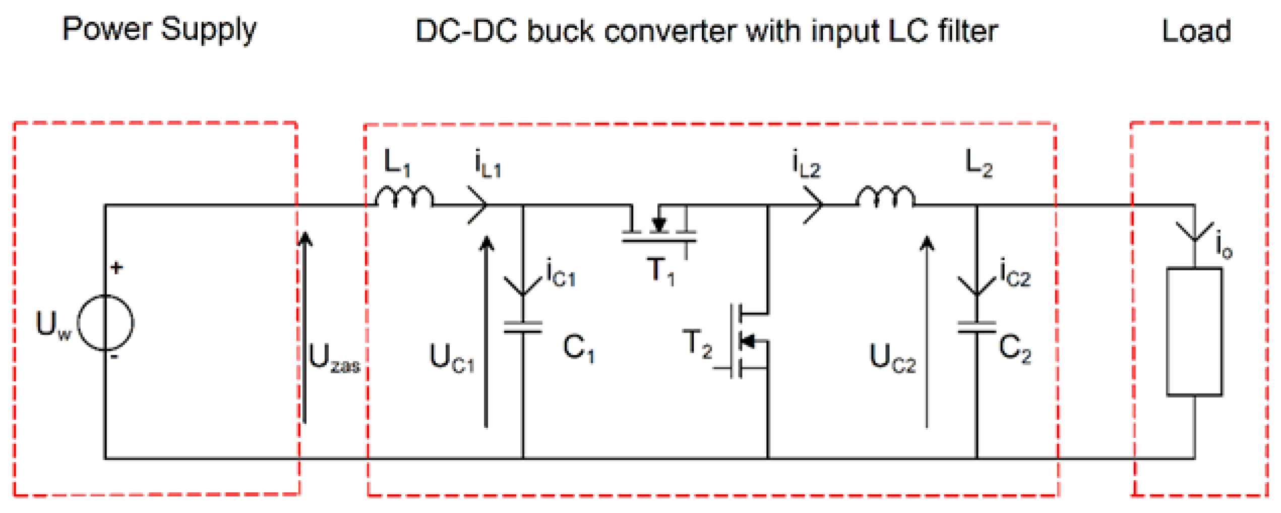
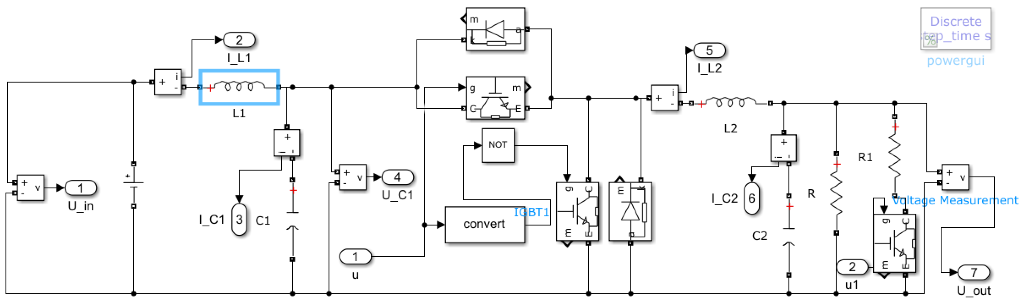
2.2. Simualtion Model of DC–DC Converter with Input LC Filter

In order to test the previously proposed control algorithms, a model of an electronic power converter with an input LC filter (Figure 4) was created in the Matlab/Simulink environment using the SimPower library.
To solve the problem of the so-called chattering, as well as to be able to use the PWM modulator, a well-known and often-used [30,31] control signal with saturation function was selected.
u = s a t ( s ) = 1 for s < e 1 e s for s e 1 for s > e
Unfortunately, in this case, a steady-state error occurs in the control system, resulting from the introduction of a continuous control law. It can be eliminated by adding an integral term to the sliding variable. Sliding variable with a damping term taking into account the voltage on the capacitor C1 takes the form
s = U z a d U C 2 + c 2 U ˙ C 2 + c 3 U C 1 U w + 1 T i ( U z a d U C 2 )
Assuming that the constant Ti of the integral term is limited and that the term itself affects only slow-changing signals significantly deviating from the frequencies important from the point of view of system stability, it can be assumed that the range of coefficients for which the closed control system is stable will not change. Parameter values calculated for sliding variables and plants from chapter 2.1 will also be valid for the discussed cases. The structure of the regulator is shown in the Figure 5.

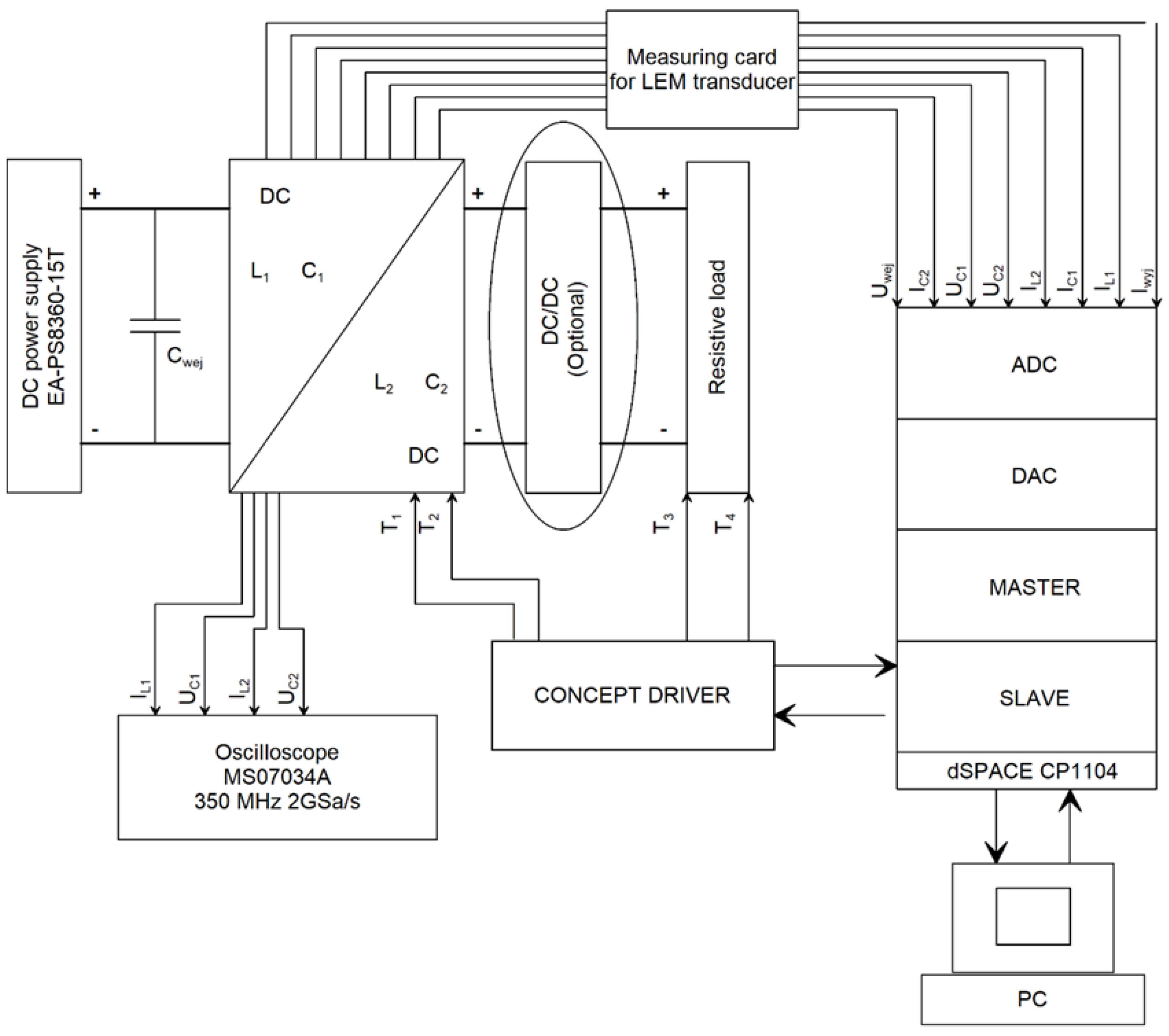
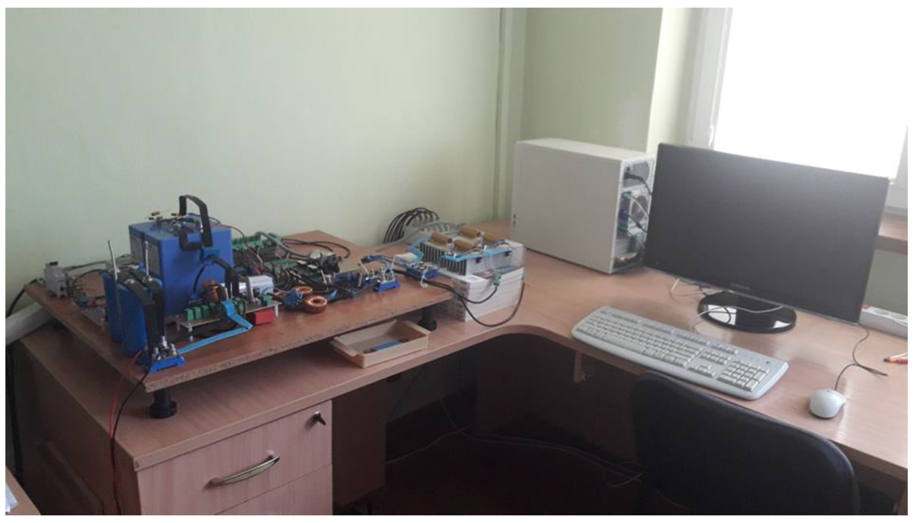
2.3. Laboratory Stand Setup

An illustrative diagram of the laboratory stand and its view are shown in the Figure 6 and Figure 7, respectively.
In Figure 6, several basic elements of the system are presented:
  • dSPACE DS1104 card, which, together with a PC computer with Matlab/Simulink and ControlDesk software installed, constitutes the acquisition and control part;
  • DC power supply with capacitance, which is the power source of the system;
  • DC–DC step-down converter with input LC filter, made in the form of a circuit placed on a printed circuit board;
  • Measurement card cooperating with LEM current and voltage converters, adjusting the voltage level for the dSPACE card;
  • 2SC0108T2A0 controllers responsible for controlling the transistors of the converter itself as well as the configurable resistive load, optional step-down DC–DC converter simulating a constant power load, four-channel oscilloscope for measuring voltages and currents of energy storage components.
Laboratory stand is illustrated in Figure 7.

3. Results

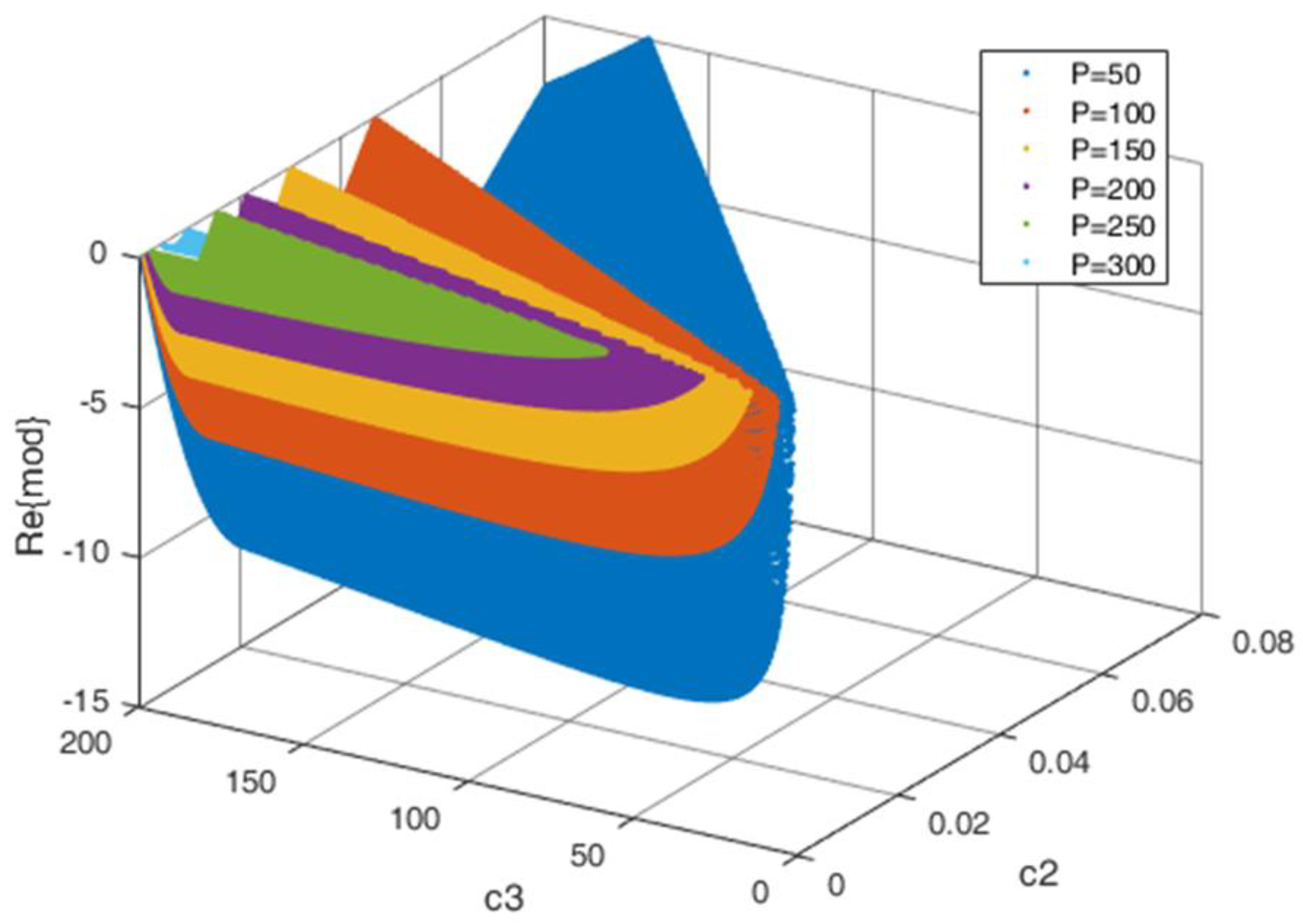
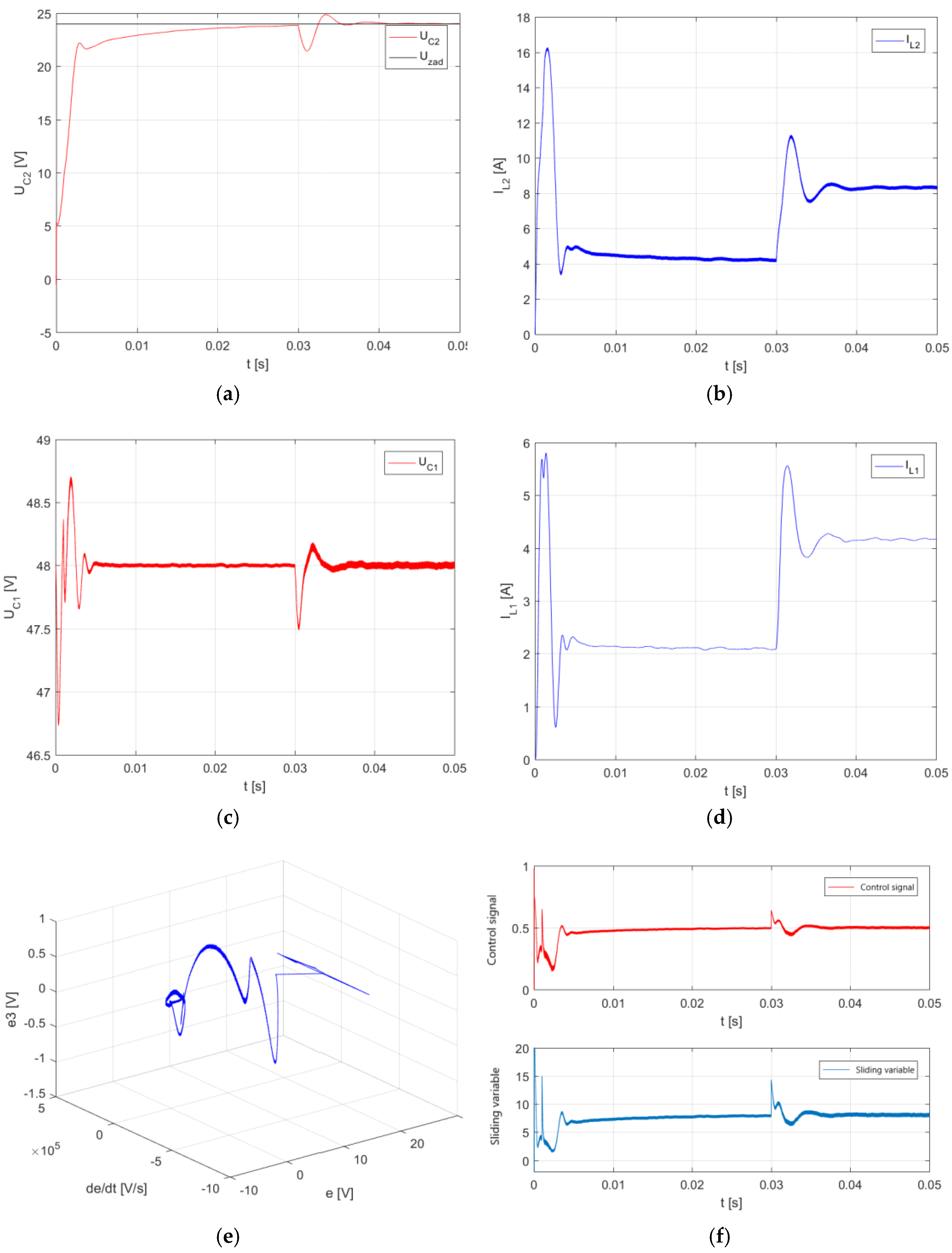
3.1. Simulation Results

The first load for which simulation tests were carried out was the resistive load. Data on the values of the system elements are taken from Table 2. The converter starts with a load of 8 Ω, and then, after 0.03 s from the start of the simulation, a step change in the load is made to the value of 4 Ω.
Figure 8 shows the waveforms of currents and voltages on the energy storage elements, the trajectory of the system, and the waveform of the control signal when the sliding variable includes the term containing the voltage on the capacitor C1, responsible for damping the oscillations of the LC input filter.
The second type of load for which simulation tests were carried out was a constant power load. The parameters of the system elements are taken from Table 2. The converter started with a load of 100 W, and then, after 0.03 s from the start of the simulation, a step load change was made to the value of 200 W.
Figure 9 shows the waveforms of currents and voltages on the energy storage elements, the trajectory of the system, and the waveform of the control signal when the sliding variable includes the term containing the voltage on the capacitor C1, responsible for the damping of the oscillations of the LC input filter.

3.2. Experimental Results

In order to demonstrate the usefulness and correctness of the analytical considerations in this chapter, laboratory tests were carried out on a step-down DC–DC converter with an input LC filter for a resistive load and a constant power load. A number of tests were carried out; each time data acquisition was performed. The following tests were carried out: an algorithm with a sliding variable not taking into account the damping term, and an algorithm with a sliding variable taking into account the voltage on the capacitor C1. The following tests of the dynamic states of the DC–DC converter with the input LC filter were carried out:
  • Start of the converter with open output terminals;
  • Start of the converter with resistive load;
  • A step change in the load from 8 Ω to 4 Ω;
  • A step change in the load from 4 Ω to 8 Ω;
  • Start of the converter with open output terminals;
  • A step change in the load from 72 W to 144 W;
  • A step change in the load from 144 W to 72 W.
The acquisition of measurement data and the control process itself were carried out using the dSPACE card. The selected signals of the system were also recorded in parallel using the MS07034A oscilloscope. Some of the research results are presented below.
Figure 10 shows the waveforms obtained for starting the converter with a load of 8 Ω where the sliding variable includes a damping term containing the voltage value on the capacitor C1. The converter is started 5 ms after the start of data acquisition.
Figure 11 shows the waveforms obtained for a step change in the converter load from 72 W to 144 W when the sliding variable includes the damping term with the voltage on the capacitor C1. A step change in load takes place 5 ms after the start of data acquisition.

4. Discussion

The aim of the study was to perform simulation and laboratory tests of sliding mode control algorithms dedicated to a DC–DC buck converter with input LC filter for both resistive and constant power loads. The experiments revealed the possibility of current and voltage input LC filter oscillation attenuation and appropriate system response at the same time by novel sliding mode variable usage. As part of the research, a novel sliding variable for a DC–DC buck converter with an input LC filter was proposed. Next, the stability of the proposed method was proven by means of equivalent control and linearization for wide range of system loads (both resistive and constant power). The next step was to develop a simulation model for the system, including the proposed control strategy. The final stage of the work was to implement the control structures in the MATLAB/Simulink environment and run them on a dSpace card controlling DC–DC buck converter with the input LC filter. The results of laboratory tests confirmed the effectiveness of the proposed method. The presented algorithm, through appropriate control, allows the reduction in the size of the filters, and the simplicity of the implementation allows it to be incorporated in industrial railway, tram, and trolleybus DC–DC converters.

Author Contributions

Methodology, P.L. and K.T.; Software, K.T.; Supervision, P.C.; Validation, P.L. and K.T.; Writing—original draft, K.T.; Writing—review & editing, P.C and K.T. All authors have read and agreed to the published version of the manuscript.

Funding

This research received no external funding.

Data Availability Statement

The data presented in this study are available on request from the corresponding author.

Conflicts of Interest

The authors declare no conflict of interest.

References

  1. Kohut, C.R. Input Filter Design Criteria for Switching Regulators Using Current-Mode Programming. IEEE Trans. Power Electron. 1992, 7, 469–479. [Google Scholar] [CrossRef]
  2. Erich, S.Y.; Polivka, W.A. Input Filter Design Criteria for Current-Programmed Regulators. IEEE Trans. Power Electron. 1992, 7, 143–151. [Google Scholar] [CrossRef]
  3. Mitchell, D.M. Power Line Filter Design Considerations for DC–DC Converters. IEEE Ind. Appl. Mag. 1999, 5, 16–26. [Google Scholar] [CrossRef]
  4. Erich, S.Y.; Polivka, W.M. Input Filter Design for Current-Programmed Regulators. In Proceedings of the Fifth Annual Proceedings on Applied Power Electronics Conference and Exposition, Los Angeles, CA, USA, 11–16 March 1990; pp. 781–791. [Google Scholar] [CrossRef]
  5. Erickson, R.W. Optimal Single Resistor Damping of Input Filters. In Proceedings of the APEC ‘99. Fourteenth Annual Applied Power Electronics Conference and Exposition, Dallas, TX, USA, 14–18 March 1999; Volume 2, pp. 1073–1079. [Google Scholar] [CrossRef]
  6. Cespedes, M.; Xing, L.; Sun, J. Constant-Power Load System Stabilization by Passive Damping. IEEE Trans. Power Electron. 2011, 26, 1832–1836. [Google Scholar] [CrossRef]
  7. Jang, Y.; Erickson, R.W. Physical Origins of Input Filter Oscillations in Current Programmed Converters. IEEE Trans. Power Electron. 1992, 7, 725–733. [Google Scholar] [CrossRef]
  8. Wu, M.; Lu, D.D.C. A Novel Stabilization Method of LC Input Filter with Constant Power Loads Without Load Performance Compromise in DC Microgrids. IEEE Trans. Ind. Electron. 2015, 62, 4552–4562. [Google Scholar] [CrossRef]
  9. Weichel, R.; Wang, G.; Mayer, J.; Hofmann, H. Active Stabilization of DC–DC Converters with Input LC Filters via Current-Mode Control and Input Voltage Feedback. In Proceedings of the 2010 IEEE Energy Conversion Congress and Exposition, Atlanta, GA, USA, 12–16 September 2010; pp. 3409–3413. [Google Scholar] [CrossRef]
  10. Dominguez, F.; Fossas, E.; Martinez, L. Stability Analysis of a Buck Converter with Input Filter via Sliding-Mode Approach. In Proceedings of the IECON’94—20th Annual Conference of IEEE Industrial Electronics, Bologna, Italy, 5–9 September 1994; Volume 3, pp. 1438–1442. [Google Scholar] [CrossRef]
  11. Malinowski, M.; Bernet, S. A Simple Voltage Sensorless Active Damping Scheme for Three-Phase PWM Converters with an LCL Filter. IEEE Trans. Ind. Electron. 2008, 55, 1876–1880. [Google Scholar] [CrossRef]
  12. Huangfu, Y.; Pang, S.; Nahid-Mobarakeh, B.; Guo, L.; Rathore, A.K.; Gao, F. Stability Analysis and Active Stabilization of On-Board DC Power Converter System with Input Filter. IEEE Trans. Ind. Electron. 2018, 65, 790–799. [Google Scholar] [CrossRef]
  13. Renaudineau, H.; Martin, J.P.; Nahid-Mobarakeh, B.; Pierfederici, S. DC–DC Converters Dynamic Modeling with State Observer-Based Parameter Estimation. IEEE Trans. Power Electron. 2015, 30, 3356–3363. [Google Scholar] [CrossRef]
  14. Joshi, P.; Seshagiri, S. Comparative Analysis of Sliding Mode Designs for DC–DC Converters. In Proceedings of the 2020 IEEE Transportation Electrification Conference & Expo (ITEC), Chicago, IL, USA, 23–26 June 2020; pp. 538–543. [Google Scholar] [CrossRef]
  15. Ni, Y.; Xu, J. Study of Discrete Global-Sliding Mode Control for Switching DC–DC Converter. J. Circuits Syst. Comput. 2012, 20, 1197–1209. [Google Scholar] [CrossRef]
  16. Hooshmandi, K.; Bayat, F.; Bartoszewicz, A. Sampled-Data Linear Parameter Variable Approach for Voltage Regulation of DC–DC Buck Converter. Electronics 2022, 11, 3208. [Google Scholar] [CrossRef]
  17. Martinez-Salamero, L.; Cid-Pastor, A.; El Aroudi, A.; Giral, R.; Calvente, J.; Ruiz-Magaz, G. Sliding-Mode Control of DC–DC Switching Converters. IFAC Proc. Vol. 2011, 44, 1910–1916. [Google Scholar] [CrossRef]
  18. He, Y.; Luo, F.L. Study of Sliding-Mode Control for DC–DC Converters. In Proceedings of the 2004 International Conference on Power System Technology, Singapore, 21–24 November 2004; Volume 2, pp. 1969–1974. [Google Scholar] [CrossRef]
  19. Mahdavi, J.; Emadi, A.; Toliyat, H.A. Application of State Space Averaging Method to Sliding Mode Control of PWM DC/DC Converters. In Proceedings of the IAS ‘97. Conference Record of the 1997 IEEE Industry Applications Conference Thirty-Second IAS Annual Meeting, New Orleans, LA, USA, 5–9 October 1997; Volume 2, pp. 820–827. [Google Scholar] [CrossRef]
  20. Guldemir, H. Sliding Mode Control of DC–DC Boost Converter. J. Appl. Sci. 2005, 5, 588–592. [Google Scholar] [CrossRef]
  21. Tan, S.C.; Lai, Y.M.; Tse, C.K. General Design Issues of Sliding-Mode Controllers in DC–DC Converters. IEEE Trans. Ind. Electron. 2008, 55, 1160–1174. [Google Scholar] [CrossRef]
  22. Guldemir, H. Study of Sliding Mode Control of DC–DC Buck Converter. Energy Power Eng. 2011, 3, 401–406. [Google Scholar] [CrossRef]
  23. Chen, Z. PI and Sliding Mode Control of a Cuk Converter. IEEE Trans. Power Electron. 2012, 27, 3695–3703. [Google Scholar] [CrossRef]
  24. Drakunov, S.V.; Reyhanoglu, M.; Singh, B. Sliding Mode Control of DC–DC Power Converters. IFAC Proc. Vol. 2009, 42, 237–242. [Google Scholar] [CrossRef]
  25. Zhao, Y.; Qiao, W.; Ha, D. A Sliding-Mode Duty-Ratio Controller for DC/DC Buck Converters with Constant Power Loads. IEEE Trans. Ind. Appl. 2014, 50, 1448–1458. [Google Scholar] [CrossRef]
  26. Zhang, F.; Yan, Y. Start-up Process and Step Response of a DCDC Converter Loaded by Constant Power Loads. IEEE Trans. Ind. Electron. 2011, 58, 298–304. [Google Scholar] [CrossRef]
  27. Sun, J.; Grotstollen, H. Averaged Modelling of Switching Power Converters: Reformulation and Theoretical Basis. In Proceedings of the PESC ‘92 Record 23rd Annual IEEE Power Electronics Specialists Conference, Toledo, Spain, 29 June–3 July 1992; pp. 1165–1172. [Google Scholar] [CrossRef]
  28. Zhu, Q. Complete Model-Free Sliding Mode Control (CMFSMC). Sci. Rep. 2021, 11, 22565. [Google Scholar] [CrossRef]
  29. Ebrahimi, N.; Ozgoli, S.; Ramezani, A. Model-Free Sliding Mode Control, Theory and Application. Proc. Inst. Mech. Eng. Part I J. Syst. Control Eng. 2018, 232, 1292–1301. [Google Scholar] [CrossRef]
  30. Šabanović, A. Sliding Modes in Power Electronics and Motion Control Systems. In Proceedings of the IECON’03. 29th Annual Conference of the IEEE Industrial Electronics Societ, Roanoke, VA, USA, 2–6 November 2003; Volume 1, pp. 997–1002. [Google Scholar] [CrossRef]
  31. Utkin, V.I. Sliding Modes in Control and Optimization. In Sliding Modes in Control and Optimization; Springer: Berlin/Heidelberg, Germany, 1992. [Google Scholar] [CrossRef]
Figure 1. DC–DC buck converter with input LC filter for resistive and constant power load.
Energies 16 06983 g001
Figure 2. Graphical representation of the least stable mode according to c2 and c3 parameters for different values of resistance.
Energies 16 06983 g002
Figure 3. Graphical representation of the least stable mode according to c2 and c3 parameters for different values of power.
Energies 16 06983 g003
Figure 4. SimPower model of DC–DC buck converter with input LC filter.
Energies 16 06983 g004
Figure 5. Regulator structure.
Energies 16 06983 g005
Figure 6. Laboratory stand diagram.
Energies 16 06983 g006
Figure 7. Laboratory stand.
Energies 16 06983 g007
Figure 8. System response for resistive load; c2 = 0.0015 s, c3 = 5, Ti = 150, and e = 8. (a) Output voltage waveform UC2; (b) output current waveform IL2; (c) input voltage waveform UC1; (d) input current waveform IL1; (e) system trajectory; (f) the waveform of the sliding variable value and the transistor control signal.
Energies 16 06983 g008
Figure 9. System response for constant power load; c2 = 0.0015 s, c3 = 5, Ti = 150, and e = 8. (a) Output voltage waveform UC2; (b) output current waveform IL2; (c) input voltage waveform UC1; (d) input current waveform IL1; (e) system trajectory; (f) the waveform of the sliding variable value and the transistor control signal.
Energies 16 06983 g009
Figure 10. Experimental results for resistive load; c2 = 0.0015 s, c3 = 5, Ti = 150, and e = 8. (a) Output voltage waveform UC2; (b) output current waveform IL2; (c) input voltage waveform UC1; (d) input current waveform IL1.
Energies 16 06983 g010
Figure 11. Experimental results for constant power load; c2 = 0.0015 s, c3 = 5, Ti = 150, and e = 8. (a) output voltage waveform UC2; (b) output current waveform IL2; (c) input voltage waveform UC1; (d) input current waveform IL1.
Energies 16 06983 g011
Table 1. Classification of input LC filter oscillation suppression.
Passive Suppression Active Suppression
Parallel to input LC filter capacitance RC series branchIn classic cascade regulators, the compensating signal addition occurs in:
  • Current regulator loop,
  • Voltage regulator loop,
  • Directly to switches.
Parallel to input LC filter inductance RL series branchFull state feedback controller
Series connection of parallel RL branch upon input LC filterAI methods (neural networks, etc.)
Oversizing of input filter parametersSMC
Table 2. DC–DC converter parameters.
Name of the ParameterValue
L1100 µH
C1600 µF
L1990 µH
C11 mF
Uzad24 V
Uw48 V
R2–12 Ω
P50–300 W
Disclaimer/Publisher’s Note: The statements, opinions and data contained in all publications are solely those of the individual author(s) and contributor(s) and not of MDPI and/or the editor(s). MDPI and/or the editor(s) disclaim responsibility for any injury to people or property resulting from any ideas, methods, instructions or products referred to in the content.

