Abstract
A three-level neutral point clamped inverter with three phase legs is often used to power three-phase electrical motors. This type of multilevel inverter has its advantages over two-level inverters. The main advantages are lower harmonic distortion and less stress on motor windings. This three-level inverter can be also used as a power source for a two-phase induction motor. A one-phase induction motor with a starting capacitor and auxiliary windings is in fact a two-phase induction motor. In this article, we show that the switching number reduction method, previously presented for use with three-phase induction motors, can be used with two-phase motors as well, after some crucial modifications. The reduction of switching decreases the switching losses. The switching number reduction is obtained with modified space vector modulation using redundant voltage vectors. The method was simulated and then implemented on a prototype 3L-NPC inverter powering a one-phase induction motor with auxiliary windings. A switching number reduction of about 19% to 29% was obtained, depending on modulation parameters.
1. Introduction
In this paper we present a method of space vector modulation (SVM) for a three-level neutral point clamped (3L-NPC) inverter that can be used to power a two-phase induction motor and that dynamically reduces the switching number, which denotes how many times the transistors are switched. Reduction of the switching number is obtained by calculating a sequence of transistor on and off states, taking into account the redundant voltage vectors of 3L-NPC. This method is based upon the method of dynamic switching number reduction for 3L-NPC powering a three-phase induction motor, which was previously presented in [1,2,3]. The switching number reduction ratio from about 19% to 29% can be achieved with the SVM parameters, which are presented in this paper.
Multilevel inverters have some major advantages compared to two-level inverters. The main advantages are less harmonic distortion of the produced voltages and currents, a smaller magnitude of voltage changes at the output (which reduces stress to isolation materials of motor windings), the capability of fault-tolerant modulation methods in case of one or more faulty switches, and the capability of using lower voltage switches in a series connection. There are also disadvantages over two-level inverters: more switching components, the need to use multilevel power supply, and more computational complexity of modulation algorithms.
New control methods for multilevel inverters are being developed by many scientists in the field of power electronics, especially for a 3L-NPC inverter, which is also used to power two-phase motors [4,5]. The work is also underway on improving the modulation techniques for a two-phase load, which can be also applied in a multilevel inverter [6]. Two-, three-, or four-leg inverters can be used to power a two-phase motor [7]. Three-leg inverters are commonly used for three-phase motors and are therefore quite accessible. Today, inverters are not used only in industries for the electric motor control. Inverters are needed also in fields such as photovoltaic systems, electric vehicles, air conditioning, home appliances, etc. Hence, it is significant to further improve their efficiency and robustness. A multilevel inverter can incorporate fault-tolerant modulation strategies, which are important, for instance, in automotive applications.
The reduction of the switching number decreases the switching losses and therefore improves the efficiency of the inverter. The efficiency improvement is strictly connected to the type of transistors used, the voltage, current, the switching frequency, and the type of load [8,9]. The presented method is adaptive and decreases the switching number under variable conditions, which may improve the efficiency of the inverter and the lifetime of its components. The switch reduction ratio is dependent on the parameters of the modulation, for instance, the frequency, modulation depth, and the switching frequency. The switch reduction ratio is a ratio between the switching number before and after using additional redundant voltage vectors, over the same time, given frequency, modulation depth, sampling period, and starting conditions.
Two is lowest number of phases that is needed for a symmetric induction electric motor to create a rotating magnetic field. This was described in one of the earliest works about polyphase induction and reluctant motors [10]. The so-called one-phase induction motors are in fact often equipped with auxiliary windings that are used in the start-up phase. The phase difference between windings is often achieved by using a capacitor in series with the auxiliary windings. There are also shaded pole induction motors with shading auxiliary windings that are used to create the second phase, which provides a rotating magnetic field to start the motor [11]. After starting, the motor can run on one phase only, but with the limited torque in comparison to the motors that use two or more phases constantly. A 3L-NPC can be used to power a two-phase induction motor, as shown in Figure 1, and maintain the rotating magnetic field [4,5,6,7]. The 3L-NPC in a two-phase configuration can be also used in a solid-state transformer that replaces a Scott-T transformer, when three- to two-phase transformation is needed.
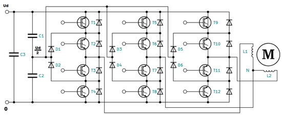
Figure 1.
Three-leg three-level NPC inverter used to power a two-phase induction motor. T1–T12 are the IGBT transistors, D1–D6 are the neutral point clamping diodes, C1–C3 are the filtering capacitors, M is the two-phase squirrel cage induction motor, and L1–L2 are its windings.
The usability of the method was confirmed by implementation on a prototype 3L-NPC inverter.
2. Space Vector Modulation with Dynamic Switching Number Reduction
The three-level NPC inverter has twelve transistors acting as switches, as shown in Figure 1. The inverter has three legs consisting of four transistors, which can give three levels of voltage, namely, 0, Ud/2, and Ud, where Ud is the input voltage. Figure 2 shows the current flow for these three levels.
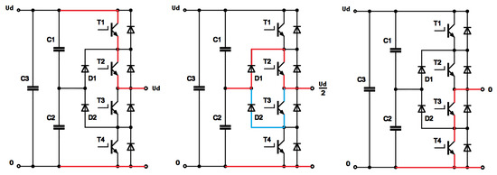
Figure 2.
Output voltages of the 3L-NPC inverter: left—Ud, center—Ud/2, right—0, red line—current flow between capacitor and output terminals, blue line—alternative flow of current for Ud/2.
The combinations of three output voltages gives nineteen possible combinations of phase-to-phase voltages. Some of those voltages can be generated by more than one combination of switching states. The six phase-to-phase voltages that can be generated by loading a C1 or C2 capacitor only are V1 to V6. The common practice is to use the redundant combinations of transistors’ switching states and alternate between them, within the Tc period, to maintain the same voltage on both capacitors [12].
In previous research, it was shown that additional switching states could be used with the proper voltage balancing method. Two and four additional states for every voltage from V1 to V6 were used in previous research [2,3]. Table 1 presents all the combinations of the current flow in the 3L-NPC inverter from Figure 1 that do not make a short circuit and that were used in this paper.

Table 1.
The switching states of the 3L-NPC inverter corresponding to the voltage vectors. The switching states are described as a 12-bit number in T1–T12 order; 0—OFF, 1—ON, *—loads C2, **—loads C1. Vectors V10 to V21 load all capacitors. Black—commonly used switching states of redundant voltage vectors; blue and orange—additional switching states; orange—switching states that do not allow flow of current both in and out of the neutral phase leg of the inverter.
All phase-to-phase voltages of 3L-NPC can be represented by voltage vectors in complex space, where they create a hexagon, as shown in Figure 3. The hexagon is not regular as in three-phase modulation, which affects the maximum usable output voltage to Ud ratio.
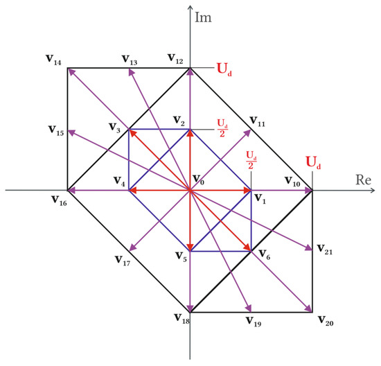
Figure 3.
Nineteen output phase-to-phase voltage vectors of the two-phase 3L-NPC inverter represented in an α–β complex space forming a hexagon.
In the SVM method, the voltage vectors are used to synthesize a U0 rotating vector [12,13]. U0 represents the rotating magnetic field and is used as a reference voltage vector, which is then approximated as a weighted average combination of three adjacent switching voltage vectors, as shown in Figure 4.
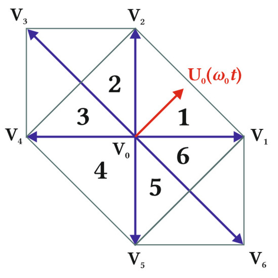
Figure 4.
One zero vector and six active voltage vectors of a two-level two-phase NPC inverter with three legs. U0 represents the rotating magnetic field and is used as a reference voltage vector. U0 is synthesized by the proper sequence of V0, V1, and V2 vectors. The vectors create a hexagon that is divided into six sectors.
The on time of each adjacent vector within the Tc period is calculated with Equations (1) and (2). The equations works with a two-level configuration. The specific equations for t1 and t2 for every sector of the hexagon are shown in Table 2.
TcU0(ω0t) = t1Vi + t2V(i+1),
t0 = Tc − t1 − t2,
Table 2.
Equations for t1 and t2 for every sector of two-level hexagon. ϑ is the angle, and ρ is the magnitude of U0 vector in polar coordinates.
The vector transposition method is used to reduce the complexity of the active time calculation of voltage vectors from three- to two-level [12]. When the U0 length, which represents the modulation depth, is longer than half of the maximum modulation, then U0 is transposed to one of six outer two-level hexagons, as shown in Figure 5.
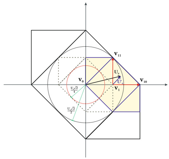
Figure 5.
Transposition of U0 coordinates to one of outer two-level hexagons, which gives the U’0. After the transposition, V1 vector is the local 0 vector. U’0 is synthesized by a combination of V1, V10, and V11 as in a two-level inverter. The outer circle represents the maximum modulation depth without overmodulation, and the inner circle represents half of the modulation depth.
There is a need to choose the appropriate outer hexagon for transposition, because all two-level hexagons have common parts of the area with the neighboring hexagons. The borders were chosen in a manner analogous to a three-phase 3L-NPC inverter [2]. The borders for transposition are shown in Figure 6. For example, if the U0 vector angle in polar coordinates is between –arcsin(√5/5) and π/4, then its coordinates are transposed to the first outer two-level hexagon, and then the times t1, t2, and t0 are computed as in a two-level inverter. The transposition of U0 to the first outer two-level hexagon is described in Cartesian coordinates with Equation (3).
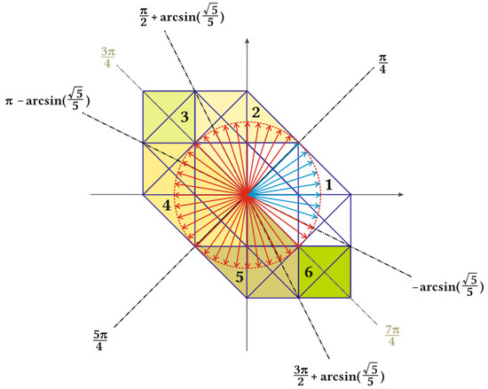
Figure 6.
Transposition borders used for transposition of U0 vector. The red circle marks the limit of maximum modulation. Red and blue denote all discrete positions of U0 for 50 Hz, full modulation, and Tc = 500 μs. Positions of U0 marked in blue are transposed to the first outer two-level hexagon. The alternative transposition borders are marked green.
If the inverter is not used in the overmodulation region, then U0 will never have to be transposed to the third and sixth outer hexagon drawn in green and light green in Figure 6. In that case, one can choose to use only four angle borders (π/4, 3π/4, 5π/4, 7π/4) and transpose U0 only to the first, second, fourth, and fifth outer hexagon accordingly.
U’0(x, y) = U0(x + 0.5Ud, y + 0Ud)
2.1. Switching Sequence, Dead Time, and the Temporal Resolution
After the computation of switching times, there is a need to define a temporal resolution if the computed times are to be used on a digital signal controller (DSC), with limitations on how often it can output synchronized signals to drive the switching transistors. In this research, the presented method was implemented on a TMS320F28379D DSC. The achieved temporal resolution (discrete resolution of time) was tr = 1 μs, which means that it is possible to set twelve transistor conducting states once every 1 μs. Therefore, the resolution of computed times was rounded to 1 μs [1].
The need for defined temporal resolution is dictated by the novel approach of the switch reduction method, which uses the additional redundant switch states for redundant vectors that are not commonly used. This method does not use ready solutions of the DSC, such as dead time management systems or counters other than ePWM modules configured to handle twelve independent outputs simultaneously every 1 μs. The method does not use the pre-computed switching sequences. The switching sequence is computed in real-time depending on the current switching state and the next voltage vector resulting from the requested U0 trajectory. The voltage vector timing is computed directly with equations from Table 2 in double floating-point form and then rounded to integer form with 1 μs resolution.
Transistors have finite times of response to driving signals. If three or four transistors are in the conducting state in one leg of the inverter, then there will be a short circuit. In order to avoid that, it was decided to use the dead time of td = 4 μs, which is the time for proper transistors to stop conducting before turning on transistors from the combination that gives the next voltage vector.
Taking into account the above-mentioned limitations, it was decided that the minimal computed time of any voltage vector should be tn = 10 μs, as shown in Figure 7a.
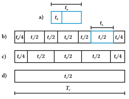
Figure 7.
Voltage vector switching sequence within a Tc sampling period.
The computed times t1, t2, and t0 were used to create a switching sequence of voltage vectors adjacent to U0. The sampling period duration was set to Tc = 500 μs for this research, which gave a 2 kHz sampling frequency. The sequence that uses all three voltage vectors is shown in Figure 7b. For the first sector of the inner two-level hexagon, the sequence of voltage vectors corresponding to computed times t1, t2, and t0 was V0, V1, V2, V0, V2, V1, and V0. The sequences for any other sector and two-level hexagon used in this research are shown in Appendix A. If one of the computed times was shorter than tn, then it was spread proportionally to the other remaining times, and then one of three vectors adjacent to U0 was not used, as shown in Figure 7c. If two of three computed times were shorter than tn, then only one voltage vector was used in the whole Tc period, as in Figure 7d. This approach gives only an insignificant rounding error and has been used successfully in [2,3].
2.2. Switching Number Reduction Method
In order to reduce the switching number, the redundant versions of the voltage vectors shown in Table 1 were used. The current state of transistors was compared with all redundant versions of the next voltage vector in a sequence by a bitwise XOR operation. The option with the least values in a binary representation of the result of bitwise operation was the option that required the smallest switching number. An example of such computations is shown in Table 3, where the next state marked orange will need the smallest number of conducting state changes in the transistors. It was found in previous research that for best results, those computations should be carried out for two steps ahead to further improve the switching number reduction.
Table 3.
Calculation of the transition from the current state of transistors to a possible version of the next voltage vector in a sequence in search of the smallest switching number.
In this method, we could use all or some of the redundant switching states shown in Table 1. However, the best results in switching number reduction were obtained when all combinations were used.
After choosing the right combination for the next voltage vector, the transition switching state should be calculated to be used for dead-time. This transition state can be calculated with bitwise AND operation between the current and the next state, as in Table 4, and then used between the current and the next active state for a td duration.
Table 4.
Calculation of the dead-time transition state.
2.3. Neutral Point Voltage Balancing
The voltage vectors V1 to V6 have redundant versions, from which some load the C1 capacitor and some others load the C2 capacitor. The sequence shown in Figure 7b is known as the symmetrical sequence, because it makes it possible to use the redundant voltage vectors for the same time in the Tc period in a way that equally loads the dividing capacitors of the 3L-NPC inverter [12], though this leads to more switching. The method of switching number reduction presented in this paper leads to a voltage imbalance. In order to use the switching number reduction method, the custom method of voltage balancing is used [2,3].
When the C1 or C2 capacitor is used, the imbalance is summed as positive and negative values of time in microseconds. If the imbalance is greater than 200 μs or lower than −200 μs, then the switching number reduction algorithm is forced to use only those of redundant vectors that load the proper capacitor to eliminate the voltage imbalance. The value of ±200 μs was chosen as the most optimal for the capacitor value in the prototype inverter, SVM parameters, and switching number reduction ratio. For example, it can be larger when using larger value capacitors.
As was found in [3], changing from redundant vectors, which load one capacitor to the vectors that load the other capacitor, should be done only when U’0 is crossing the border between sectors of two-level hexagon regardless of the assumed value of the imbalance in microseconds. This greatly reduces the number of voltage spikes occurring during the change.
3. Implementation on Prototype Inverter
The switching number reducing method was implemented on a TMS320F28379D dual-core microcontroller using both cores. One core was used to calculate the U0 trajectory for the given parameters of the drive (for instance voltage and frequency), the SVM voltage vectors sequence, and the transistor’s switching sequence with the switching number reduction. The other was used to buffer those sequences and send them to output with the proper timing to drive the IGBT transistors. The non-standard application of the ePWM modules of the DSC sets the twelve independent outputs simultaneously and uses almost all computing power of one of its cores. For this reason, the method needed dual-core implementation. The specifics of microcontroller implementation were described in detail in [1,2,3].
The power section of the prototype inverter consisted of the main components listed in Table 5. The power section of the inverter was the same as that used in previously presented research [2]. Therefore, it was possible to use 3L-NPC to power another type of motor by changing the controlling software.
Table 5.
The list of main components of the prototype inverter.
The inverter was used to power a Lucas-Nuelle SE2672-3P one-phase squirrel-cage induction motor in a two-phase configuration that treats the auxiliary windings as the second-phase windings, as shown in Figure 1. The nominal parameters of the motor used in a one-phase configuration are U = 230 V, I = 2.9 A, P = 0.37 kW, f = 50Hz, 2870 rpm. The main and auxiliary windings are not the same in one-phase motors, which gave an opportunity to test the application of different redundant switching states under the asymmetrical load.
The measurements were carried out using the following equipment connected as shown in Figure A1:
- National Instruments PXIe-1062Q (with two PXI-6133 and two BNC-2120 modules) for the data acquisition,
- Two differential amplifiers (PE-5310-2B) for the purpose of measuring the output voltage,
- Three LEM 50 A/0.5 V current probes, for measuring the output current,
- SICK DFS60B-S4PA10000 incremental encoder.
4. Results
The SVM parameters were described in Section 2.1. The input voltage was set to Ud = 460 V to obtain the nominal voltages for the motor. This value was calculated as Ud = 2√2∙Uin, where Uin is the nominal RMS input voltage of each phase of the motor. The maximum output voltage of the inverter (without overmodulation) relative to Ud is shown in Figure 5.
In steady state measurements, the motor was loaded with 1.23 Nm of torque. The frequency was set to 50 Hz, and the modulation index was set to full, which gave about 230 V phase voltage. The trajectory of U0 under those conditions is shown on Figure 6. The method used three sets of redundant switching states from Table 1: A—standard (marked black), B—all states, and C—states marked black along with blue.
The measurements were performed to compare the quality of the output waveforms in relation to the applied sets of redundant switching states. The output voltages for sets A, B, and C are shown in Figure 8, Figure 9 and Figure 10. The output currents are shown in Figure 11, Figure 12 and Figure 13. As can be seen on those figures, there was no apparent difference in output waveforms in relation to the set used. Output currents were showing clear signs of asymmetric load between the two windings of the motor. The main phase drew the most current under load.
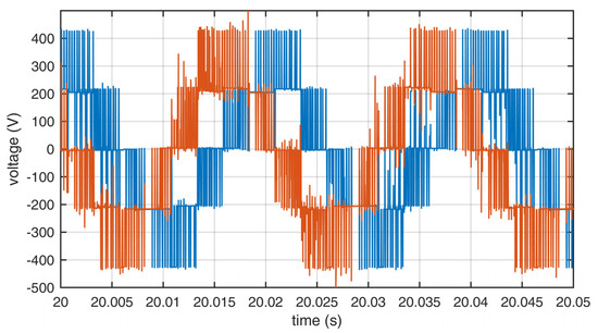
Figure 8.
Output line voltages of the inverter using set A. Blue—L1, red—L2.
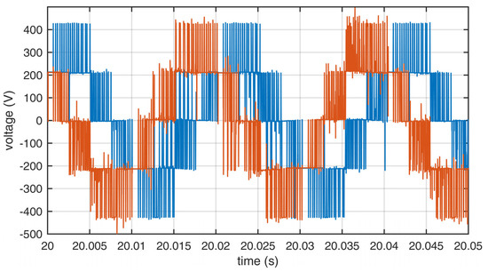
Figure 9.
Output line voltages of the inverter using set B. Blue—L1, red—L2.
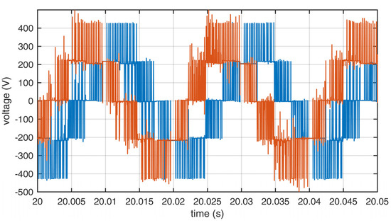
Figure 10.
Output line voltages of the inverter using set C. Blue—L1, red—L2.
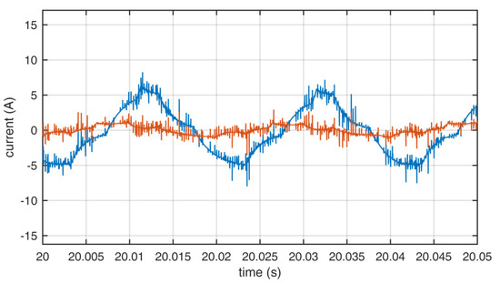
Figure 11.
Output currents of the inverter using set A. Blue—L1, red—L2.
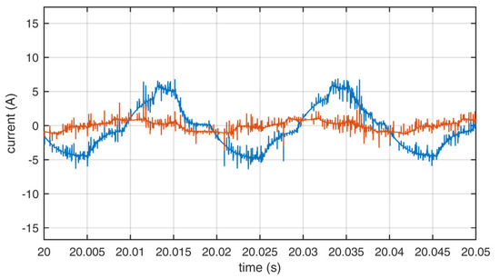
Figure 12.
Output currents of the inverter using set B. Blue—L1, red—L2.
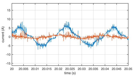
Figure 13.
Output currents of the inverter using set C. Blue—L1, red—L2.
A spectral analysis was performed, which showed a high level of odd and even harmonics in voltage and current due to the asymmetric load. In comparison, the most unwanted harmonics were present when set B was used. The THD values were computed from the measurements and are presented in Table 6. The values of THD clearly showed that when set B was used instead of the standard A set, the THD levels were much larger than when set C was used to reduce the switching number. This was predicted by the authors, because set B did not always allow for the current to flow in and out of the neutral leg in the time of one switching state, which disrupted the flow of unwanted current induced in the asymmetric motor windings. In the case of current, the THD levels were smaller when using set C than when set A was applied. When set A was used, the most pronounced harmonics were the 5th, 3rd, and 11th in phase L1 and the 5th, 7th, and 11th in phase L2 for voltage; and the 3rd, 5th, 4th, and 11th in phase L1 and the 3rd, 5th, 2nd, and 7th in phase L2 for current. When set B was used, the most pronounced harmonics were the 5th, 3rd, and 11th in phase L1 and the 5th, 7th, 17th, and 11th in phase L2 for voltage; and the 3rd, 5th, and 11th in phase L1 and the 3rd, 5th, and 7th in phase L2 for current. When using set B, there were also high inter-harmonics of 25 Hz multiples with values close to the main harmonics. When set C was used, the most pronounced harmonics were the 5th, 3rd, and 11th in phase L1 and the 5th, 7th, and 11th in phase L2 for voltage; and the 3rd, 5th, 2nd, and 4th in phase L1 and the 3rd, 5th, 7th, and 4th in phase L2 for current. There were similar harmonic contents of the waveforms generated when using either set A or C.
Table 6.
THD of output voltages and currents of the inverter—1 s window.
The switching number for two seconds of modulation with parameters described in this paper is presented in Table 7. The use of set A required the greatest amount of switching, and the use of set B needed the smallest amount of switching at the cost of a higher THD. The use of set C offered a reduction in the switching number with a lower impact on the THD levels. As with the previous three-phase implementation, the switching number reduction was dependent mainly on the modulation depth. When the B or C set was used, the reduction started at more than a half of the modulation depth and increased to its maximum at the full modulation.
Table 7.
The switching number for 2 s of full modulation, 50 Hz.
The dynamic state was measured with the same basic parameters as in the steady state. The frequency and the modulation index were variable. There was no load on the motor. The U/f ratio was constant. The desired speed was set to the linear acceleration from 0 to 3000 rpm over 1 s, 3000 rpm steady for 1 s, 3000 rpm to −3000 rpm in 2 s, −3000 rpm over 1 s, and then deceleration from −3000 rpm to 0 in 1 s. The negative rpm stands for rotation in the opposite direction. First, the A set was used for the described dynamic state, and then the C set was used in measurements to compare the waveforms. The PI control with the wind-up protection was used to achieve the desired speeds of the motor. The waveforms of voltage are shown in Figure 14, and current values are shown in Figure 15.
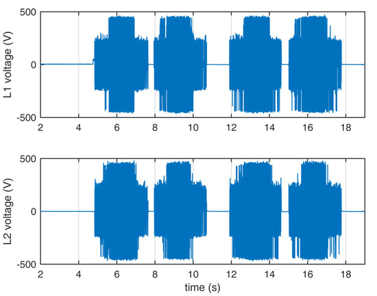
Figure 14.
Voltage waveforms of the dynamic state. The first half of the measurement uses set A, while the other half uses set C.
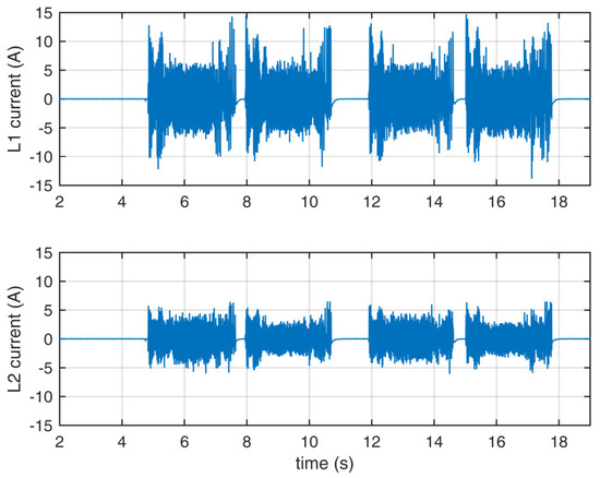
Figure 15.
Current waveforms of the dynamic state. The first half of the measurement uses set A, while the other half uses set C.
The waveforms of the current were similar between set A and set C. There were more overvoltage spikes in the voltage waveform when set C was used in comparison to set A, though those differences were minimal. Set B, not shown here, gave the most unwanted voltage spikes. In each case, the achieved rotational speeds were similar. As with the steady state, the use of set C was more practical than the use of set B to reduce the switching number.
5. Discussion and Conclusions
The main goal of the presented research was to assess whether the method of the switch reduction previously used with a 3L-NPC and three-phase motor can be applied with the same inverter hardware and two-phase motor and what impact it will have on the quality of the output waveforms. It was crucial to find what redundant switching states from all combinations of the V1 to V6 voltage vectors yielded the best results within the two-phase configuration. The research has shown that it is possible to use all redundant states of V1 to V6 voltage vectors to lessen the switching number by almost 29% using the presented method of modulation with the disadvantage of the higher THD levels. It was also shown that, by using only those redundant voltage vectors that allow for flow of current in and out of the neutral leg, an almost 19% reduction of switching number can be achieved with almost the same levels of THD.
This paper presented both the theoretical and practical implementation of the reduction method. The research results indicate that the real-time switching number reduction method is very adaptive, and it can be used in 3L-NPC in two-phase configuration after the proper modifications of the SVM part of the algorithm. The method can apply the commonly used redundant switching states as well as all other valid redundant combinations. The reduction of the switching number lessens the switching losses. The main cost of using this method is the computational complexity that requires a dual-core digital signal processor at its present implementation. In future research, the feasibility of implementing the method on a single-core processor will be assessed.
Author Contributions
Conceptualization, K.R. and R.B.; methodology, R.B.; software, K.R. and K.G.; validation, R.B.; formal analysis, R.B. and K.R.; investigation, R.B., K.G., and K.R.; resources, K.G.; data curation, R.B. and K.R.; writing—original draft preparation, K.R.; writing—review and editing, R.B. and K.G.; visualization, K.R.; supervision, R.B.; project administration, R.B.; funding acquisition, R.B. and K.G. All authors have read and agreed to the published version of the manuscript.
Funding
This research received no external funding.
Institutional Review Board Statement
Not applicable.
Informed Consent Statement
Not applicable.
Data Availability Statement
Not applicable.
Conflicts of Interest
The authors declare no conflict of interest.
Appendix A
The voltage vector switching sequences corresponding to every sector of every two-level hexagon used in this research are shown in Table A1, Table A2, Table A3, Table A4, Table A5, Table A6 and Table A7. These sequences were used in the previous versions of the switching number reduction method in [1,2,3].
Table A1.
Vector switching sequences of the inner hexagon, by the ith designation (Vi).
Table A1.
Vector switching sequences of the inner hexagon, by the ith designation (Vi).
| Sector | Vector Sequence |
|---|---|
| 1 | 0, 1, 2, 0, 2, 1, 0 |
| 2 | 0, 3, 2, 0, 2, 3, 0 |
| 3 | 0, 3, 4, 0, 4, 3, 0 |
| 4 | 0, 5, 4, 0, 4, 5, 0 |
| 5 | 0, 5, 6, 0, 6, 5, 0 |
| 6 | 0, 1, 6, 0, 6, 1, 0 |
Table A2.
Vector switching sequences of the first outer hexagon, by the ith designation (Vi).
Table A2.
Vector switching sequences of the first outer hexagon, by the ith designation (Vi).
| Sector | Vector Sequence |
|---|---|
| 1 | 1, 10, 11, 1, 11, 10, 1 |
| 2 | 1, 2, 11, 1, 11, 2, 1 |
| 3 | 1, 2, 0, 1, 0, 2, 1 |
| 4 | 1, 6, 0, 1, 0, 6, 1 |
| 5 | 1, 6, 21, 1, 21, 6, 1 |
| 6 | 1, 10, 21, 1, 21, 10, 1 |
Table A3.
Vector switching sequences of the second outer hexagon, by the ith designation (Vi).
Table A3.
Vector switching sequences of the second outer hexagon, by the ith designation (Vi).
| Sector | Vector Sequence |
|---|---|
| 1 | 2, 11, 12, 2, 12, 11, 2 |
| 2 | 2, 13, 12, 2, 12, 13, 2 |
| 3 | 2, 13, 3, 2, 3, 13, 2 |
| 4 | 2, 0, 3, 2, 3, 0, 2 |
| 5 | 2, 0, 1, 2, 1, 0, 2 |
| 6 | 2, 11, 1, 2, 1, 11, 2 |
Table A4.
Vector switching sequences of the third outer hexagon, by the ith designation (Vi).
Table A4.
Vector switching sequences of the third outer hexagon, by the ith designation (Vi).
| Sector | Vector Sequence |
|---|---|
| 1 | 3, 2, 13, 3, 13, 2, 3 |
| 2 | 3, 14, 13, 3, 13, 14, 3 |
| 3 | 3, 14, 15, 3, 15, 14, 3 |
| 4 | 3, 4, 15, 3, 15, 4, 3 |
| 5 | 3, 4, 0, 3, 0, 4, 3 |
| 6 | 3, 2, 0, 3, 0, 2, 3 |
Table A5.
Vector switching sequences of the fourth outer hexagon, by the ith designation (Vi).
Table A5.
Vector switching sequences of the fourth outer hexagon, by the ith designation (Vi).
| Sector | Vector Sequence |
|---|---|
| 1 | 4, 0, 3, 4, 3, 0, 4 |
| 2 | 4, 15, 3, 4, 3, 15, 4 |
| 3 | 4, 15, 16, 4, 16, 15, 4 |
| 4 | 4, 17, 16, 4, 16, 17, 4 |
| 5 | 4, 17, 5, 4, 5, 17, 4 |
| 6 | 0, 1, 6, 0, 6, 1, 0 |
Table A6.
Vector switching sequences of the fifth outer hexagon, by the ith designation (Vi).
Table A6.
Vector switching sequences of the fifth outer hexagon, by the ith designation (Vi).
| Sector | Vector Sequence |
|---|---|
| 1 | 5, 6, 0, 5, 0, 6, 5 |
| 2 | 5, 4, 0, 5, 0, 4, 5 |
| 3 | 5, 4, 17, 5, 17, 4, 5 |
| 4 | 5, 18, 17, 5, 17, 18, 5 |
| 5 | 5, 18, 19, 5, 19, 18, 5 |
| 6 | 5, 6, 19, 5, 19, 6, 5 |
Table A7.
Vector switching sequences of the sixth outer hexagon, by the ith designation (Vi).
Table A7.
Vector switching sequences of the sixth outer hexagon, by the ith designation (Vi).
| Sector | Vector Sequence |
|---|---|
| 1 | 6, 21, 1, 6, 1, 21, 6 |
| 2 | 6, 0, 1, 6, 1, 0, 6 |
| 3 | 6, 0, 5, 6, 5, 0, 6 |
| 4 | 6, 19, 5, 6, 5, 19, 6 |
| 5 | 6, 19, 20, 6, 20, 19, 6 |
| 6 | 6, 21, 20, 6, 20, 21, 6 |
The schematic of the experimental setup used in measurements of steady and dynamic states is presented in Figure A1.

Figure A1.
Schematic of experimental setup.
Figure A1.
Schematic of experimental setup.

References
- Górecki, K.; Rogowski, K.; Beniak, R. Three-level NPC Inverter SVM Implementation on Delfino DSC. In Proceedings of the 16th IFAC Conference on Programmable Devices and Embedded Systems, High Tatras, Slovakia, 29–31 October 2019. [Google Scholar] [CrossRef]
- Beniak, R.; Górecki, K.; Paduch, P.; Rogowski, K. Reduced Switch Count in Space Vector PWM for Three-Level NPC Inverter. Energies 2020, 13, 5945. [Google Scholar] [CrossRef]
- Rogowski, K. Optimization Methods for Three-Level NPC Inverter Control. Ph.D. Thesis, Opole University of Technology, Opole, Poland, 2021. [Google Scholar]
- Zhang, G.; Wan, Y.; Wang, Z.; Gao, L.; Zhou, Z.; Geng, Q. Discontinuous Space Vector PWM Strategy for Three-Phase Three-Level Electric Vehicle Traction Inverter Fed Two-Phase Load. World Electr. Veh. J. 2020, 11, 27. [Google Scholar] [CrossRef]
- Kang, J.-W.; Hyun, S.-W.; Kan, Y.; Lee, H.; Lee, J.-H. A Novel Zero Dead-Time PWM Method to Improve the Current Distortion of a Three-Level NPC Inverter. Electronics 2020, 9, 2195. [Google Scholar] [CrossRef]
- Srirattanawichaikul, W. A generalized switching function-based discontinuous space vector modulationtechnique for unbalanced two-phase three-leg inverters. Turk. J. Electr. Eng. Comp. Sci. 2019, 27, 1157–1171. [Google Scholar] [CrossRef]
- Jang, D.-H. Novel PWM Techniques for Two-Leg, Four-Leg and Three-Leg Two-Phase Inverters. In Proceedings of the Fourtieth IAS Annual Meeting. Conference Record of the 2005 Industry Applications Conference, Hongkong, China, 2–6 October 2005. [Google Scholar] [CrossRef]
- Feix, G.; Dieckerhoff, S.; Allmeling, J.; Schonberger, J. Simple Methods to Calculate IGBT and Diode Conduction and Switching Losses. In Proceedings of the 13th European Conference on Power Electronics and Applications, Barcelona, Spain, 8–10 September 2009. [Google Scholar]
- Drofenik, U.; Kolar, J.W. A General Scheme for Calculating Switching-and Conduction-Losses. In Proceedings of the 5th International Power Electronics Conference, IPEC-Niigata, Himeji, Japan, 18–21 May 2005. [Google Scholar]
- Tesla, N. Electro-Magnetic Motor. U.S. Patent 381968, 1 May 1888. [Google Scholar]
- Thomson, E. Alternating-Current Magnetic Device. U.S. Patent 428650, 27 May 1890. [Google Scholar]
- Holmes, D.G.; Lipo, T.A. Pulse Width Modulation for Power Converters: Principles and Practice; IEEE Press: Piscataway, NJ, USA, 2003. [Google Scholar]
- Van der Broeck, H.W.; Skudelny, H.-C.; Stanke, G.V. Analysis and realization of a pulsewidth modulator based on voltage space vectors. IEEE Trans. Ind. Appl. 1988, 24, 142–150. [Google Scholar] [CrossRef]


Disclaimer/Publisher’s Note: The statements, opinions and data contained in all publications are solely those of the individual author(s) and contributor(s) and not of MDPI and/or the editor(s). MDPI and/or the editor(s) disclaim responsibility for any injury to people or property resulting from any ideas, methods, instructions or products referred to in the content. |
© 2023 by the authors. Licensee MDPI, Basel, Switzerland. This article is an open access article distributed under the terms and conditions of the Creative Commons Attribution (CC BY) license (https://creativecommons.org/licenses/by/4.0/).