Perspective

Perspective of Voltage-Fed Single-Phase Multilevel DC-AC Inverters

1
Department of Electrical Engineering, Feng Chia University, Taichung 40724, Taiwan
2
Department of Electrical Engineering, National Taipei University of Technology, Taipei 10608, Taiwan
*
Author to whom correspondence should be addressed.
Energies 2023, 16(2), 898; https://doi.org/10.3390/en16020898
Submission received: 25 November 2022 / Revised: 3 January 2023 / Accepted: 9 January 2023 / Published: 12 January 2023

Abstract

:
Standing out for their remarkable benefits, such as lower voltage stress on integrated semiconductor devices, reduction in total harmonic distortion, as well as lower electromagnetic effects, multilevel inverters (MLIs) increase their share in the field of energy supply. The multilevel inverter is an interesting research topic that realizes the generation of desired output voltage waveforms composed of small voltage steps. However, many studies have put a premium on the structure, efficiency, and output of the multilevel inverter, but there are relatively few studies on the THD and practical product applications. Consequently, in this brief perspective, some puzzles for MLIs are pointed out to explore new ideas as well as to present new questions.

1. Introduction

Multilevel DC-AC inverters (MLIs) are able to set specific DC voltage levels directly to generate a desired AC voltage at the inverter’s output terminals. Hence, MLIs are a preferrable solution for AC power supplies, including interfacing photovoltaic energy systems [1], low-voltage wind energy systems [2], fuel cell energy conversion systems [3], chargers of fully electric vehicles [4], on-board in hybrid and fully electric vehicles [5] and off-board for electric buses [6], high-voltage renewable energy systems [7], as well as renewable energy conversion applications, such as reducing wind energy costs [8] and improving the efficiency [9] and reliability of photovoltaic energy systems [10] because their ability of low voltage stress, high efficiency, low common-mode voltage [11] provides high-quality output waveforms and improves the total harmonic distortion (THD) [12].
The basic operating principle of the multilevel DC-AC inverter is to utilize the switch path to make the output voltage stratified and to increase the number of voltage levels or filters to lead to the output voltage being sinusoidal-like. Since the output voltage of a multilevel DC-AC inverter is a stratified output voltage, the voltage stress on the switch can be clamped. Therefore, the high-voltage AC output can be constructed by low-voltage-withstanding components.
On the one hand, MLIs can be classified into two major categories, single-phase MLIs and three-phase MLIs. In general, three-phase MLIs have the advantage that all semiconductors are rated to the same voltage, despite the ratio of voltage levels over the number of power semiconductors being relatively low compared to low-power converters. Single-phase MLIs are also a wide research field in which a large number of voltage levels can be realized by sacrificing the voltage rating of semiconductors.
On the other hand, MLIs can be also classified into two categories for different applications, current-fed MLIs and voltage-fed MLIs. Since the voltage-fed MLI has low THD, it can be applied in many industrial applications, such as AC motors to reduce the torque ripple, low-frequency transformers to reduce the core loss, and utility parallel of green power with relatively low electric pollution.
Voltage-fed single-phase MLIs can be mainly classified into three types, based on symmetrical structure and processing power, including neutral point clamp, the flywheel capacitor type, and series-connected-based type [13].
The neutral point clamp can be furthermore classified into active neutral point clamped (ANPC) and diode clamp. The active neutral point clamped is based on NPC, and can be classified by switched capacitors, T-type, F-type, K-type, and Class-D-type. Figure 1 shows the classification of the voltage-fed single-phase MLI.

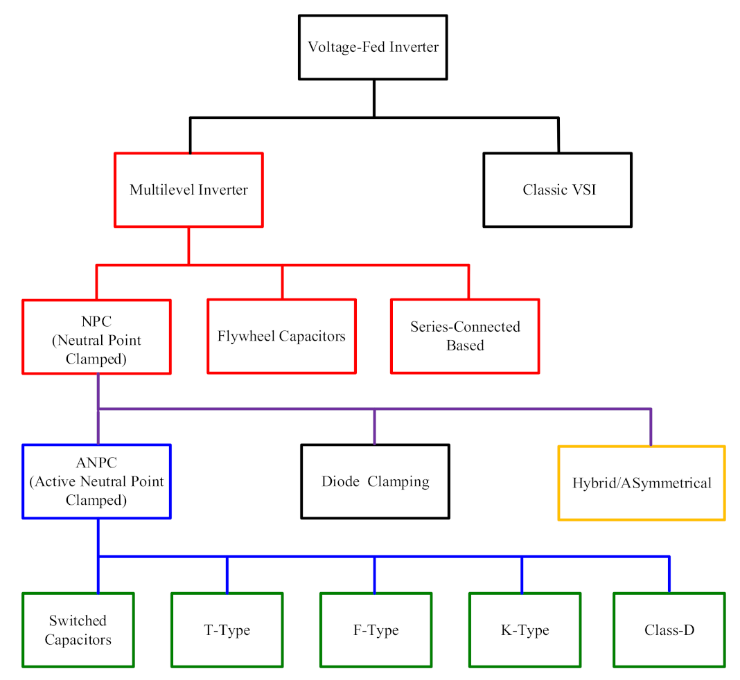
2. Analysis of Basic Topologies of Systematic MLIs

In this section, we will analyze and explain the operation principles of three typical symmetrical structures of the five-level inverter: neutral point clamped, flywheel capacitors, and series-connected-based, as displayed in Figure 1.

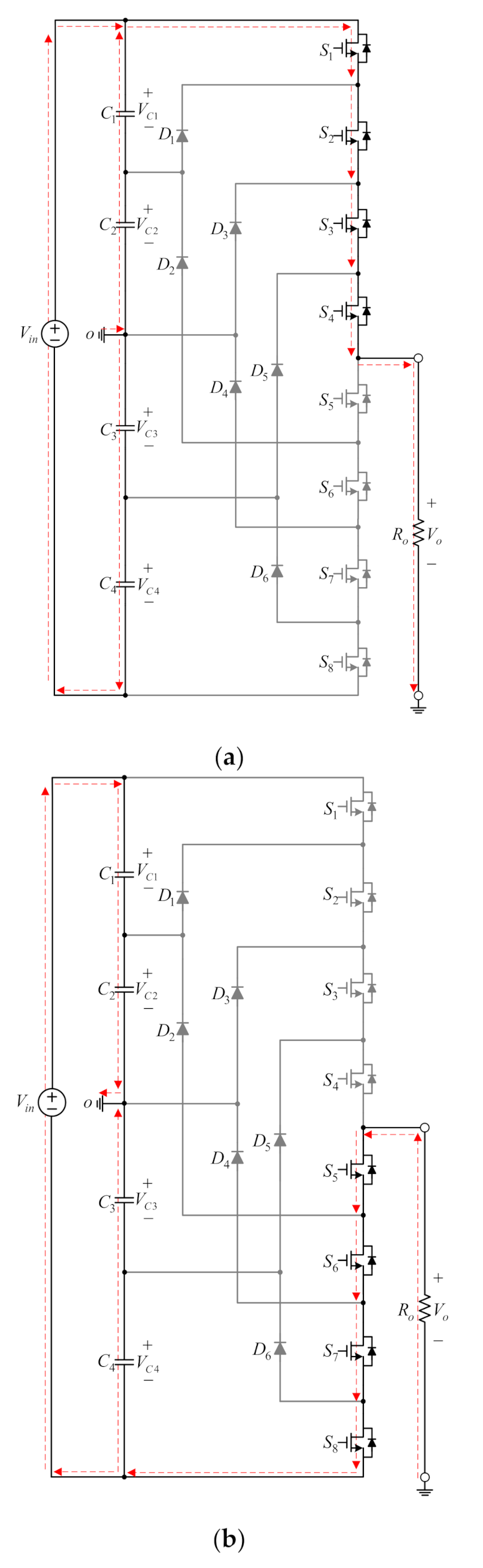
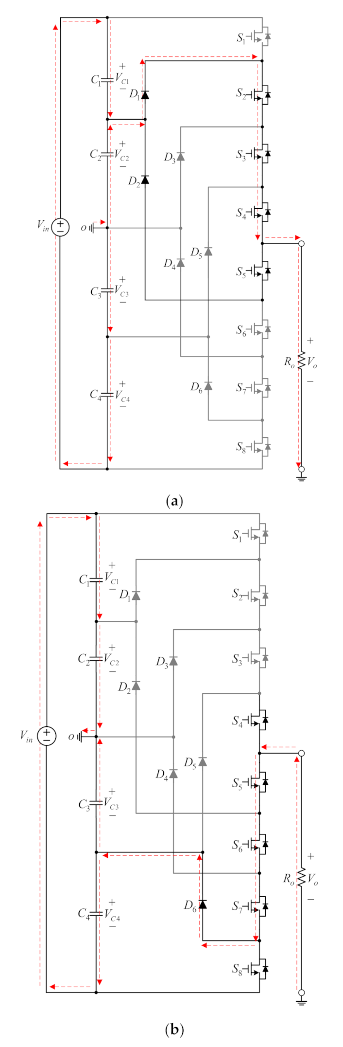
2.1. Neutral Point Clamped Inverter

Figure 2 displays the five-level neutral point clamped (NPC) inverter circuit structure, which consists of eight switches S1, S2, S3, S4, S5, S6, S7, and S8, six clamping diodes D1, D2, D3, D4, D5, and D6, four DC-link capacitors C1, C2, C3, and C4, and one output load resistor Ro, where Vin is the DC input voltage, Vo is the AC output voltage, and ‘o’ is the neutral point [14]. The operation of the inverter is described below. It is noted that each red line and arrow shows the current flow.
Status I [Vo = 0]: As displayed in Figure 3, switches S1, S2, S7, and S8 are cut off, while the switches S3, S4, S5, and S6 are on, so the output voltage Vo is zero.
Status II [Vo = 0.5 Vin or −0.5 Vin]: When the switches S1, S2, S3, and S4 are on and S5, S6, S7, and S8 are off, the circuit is displayed in Figure 4a, and the output voltage is 0.5 Vin. When the switches S5, S6, S7, and S8 are on and S1, S2, S3, and S4 are off, the circuit is displayed in Figure 4b, and the output voltage is 0.5 Vin.
Status III [Vo = 0.25 Vin or −0.25 Vin]: When the switches S2, S3, S4, and S5 are on and S1, S6, S7, and S8 are off, the circuit is displayed in Figure 5a, and the output voltage is 0.25 Vin. When the switches S4, S5, S6, and S7 are on and S1, S2, S3, and S8 are off, the circuit is displayed in Figure 5b, and the output voltage is −0.25 Vin.
For an m-level flywheel diode clamped inverter, the required number of components is displayed in Equations (1)–(3).
Number of switches of an m-level flywheel diode clamped inverter: 2(m − 1)
Number of diodes of an m-level flywheel diode clamped inverter: 2(m − 2)
Number of capacitors of an m-level flywheel diode clamped inverter: m − 1
The NPC multilevel power inverter is used to generate the output terminal potential by clamping diodes to the neutral point [15]. However, when the number of voltage levels increases, more clamping diodes, semiconductor switches, and DC-link capacitors are required. As more clamping diodes are connected in series to block the higher voltage, more conduction losses are created, and reverse recovery currents are yielded, thereby increasing the switching losses.

2.2. Flywheel Capacitor Inverter

A flywheel capacitor inverter has a similar circuit structure to a diode clamping circuit, but the two structures and principles are different. The diode clamping inverter uses diode clamping voltage to achieve a hierarchical output voltage, while the flywheel capacitor inverter uses balanced capacitance to achieve a hierarchical output voltage.
Figure 6 shows the five-level flywheel capacitor inverter circuit structure which consists of eight switches S1, S2, S3, S4, S5, S6, S7, and S8, ten DC-link capacitors C1, C2, C3, C4, C5, C6, C7, C8, C9, and C10, and one output load resistor Ro, where Vin is the DC input voltage, Vo is the AC output voltage, and ‘o’ is the neutral point of the DC input voltage [16]. The operation of the inverter is described below, where the voltage across all capacitors is 0.25 Vin.
Status I [Vo = 0]: When the switches S1, S4, S6, and S7 are on, and switches S2, S3, S5, and S8 are off, the circuit is displayed in Figure 7a, and the output voltage is zero. When the switches S2, S3, S5, and S8 are on and S1, S4, S6, and S7 are off, the circuit is displayed in Figure 7b, and the output voltage is zero.
Status II [Vo = 0.5 Vin or −0.5 Vin]: When the switches S1, S2, S3, and S4 are on and the switches S5, S6, S7, and S8 are off, the circuit is displayed in Figure 8a, and the output voltage is 0.5 Vin. When the switches S5, S6, S7, and S8 are on and the switches S1, S2, S3, and S4 are off, the circuit is displayed in Figure 8b, and the output voltage Vo is −0.5 Vin.
Status III [Vo = 0.25 Vin or −0.25 Vin]: When the switches S1, S2, S4, and S6 are on and the switches S3, S5, S7, and S8 are off, the circuit is displayed in Figure 9a, and the output voltage is 0.25 Vin. When the switches S3, S5, S7, and S8 are on and the switches S1, S2, S4, and S6 are off, the circuit is displayed in Figure 9b, and the output voltage Vo is −0.25 Vin.
For an m-level flywheel capacitor inverter, the required number of components is shown in Equations (4) and (5).
Number of switches of an m-level flywheel capacitor inverter: 2(m − 2)
Number of capacitors of an m-level flywheel capacitor inverter: 0.5m(m − 1)
The flywheel-capacitor-based multilevel DC-AC inverter is designed to realize the AC output voltage clamped by interconnecting multiple capacitors [17]. However, a large number of capacitors and complex control methods for capacitor voltage balancing are required to achieve a hierarchical output voltage.

2.3. Series-Connected-Based Inverter

A series-connected-based inverter is a circuit in which two or more identical H-bridge circuits are connected in series, and the number of series connections is adjusted according to the number of levels and output voltage required. Instead of using capacitors and diodes to clamp the output voltage, this type of circuit uses multiple power supplies to form the step voltage and operates the switches in unipolar switching to realize the output step AC voltage. Therefore, the maximum value of the output sine wave voltage is equal to the sum of all power supply voltages.
Figure 10 shows the circuit structure of a five-level series-connected inverter circuit structure which consists of eight switches S1, S2, S3, S4, S5, S6, S7, and S8 to form an H-bridge circuit and one output load resistance Ro, where Vin is the DC input voltage, and Vo is the AC output voltage [18]. The operation of the inverter is described below.
Status I [Vo = 0]: As displayed in Figure 11, all the switches are cut off in this state. Therefore, the output voltage Vo is zero, and there is no loop in the circuit.
Status II [Vo = Vin or −Vin]: When the switches S4, S5, and S8 are on, and the switches S1, S2, S3, S7, and S6 are off, the circuit is displayed in Figure 12a, and the energy of Vin will be transferred to the load through S4, S5, S8 and the body diode of S2, so the output voltage Vo is Vin. When the switches S2, S3, and S6 are on, and the switches S1, S4, S5, S7, and S8 are off, the circuit is displayed in Figure 12b, and the energy of the input voltage Vin will be transferred to the load through S2, S3, S6 and the body diode of S8, so the output voltage Vo is −Vin.
Status III [Vo = 2 Vin or −2 Vin]: When the switches S1, S4, S5, and S8 are on, and the switches S2, S3, S6, and S7 are off, the output voltage is 2 Vin, and the circuit is displayed in Figure 13a. When the switches S3, S5, S7, and S8 are on, and the switches S1, S2, S4, and S6 are off, the output voltage is −2 Vin, and the circuit is displayed in Figure 13b.
For an m-level series-connected inverter, the number of components required is shown in Equations (6) and (7).
Number of switches of an m-level series-connected inverter: 2(m − 1)
Number of power supplies of an m-level series-connected inverter: 0.5(m − 1)
The series-connected-based multilevel DC-AC inverter is the only type having a modular design concept and adopts the fewest components among the three types [19]. However, the need for multiple independent power supplies to synthesize the required levels of the AC output voltage limits its applications.
Based on the above analysis, Table 1 displays the switching status of the systematic five-level MLIs and its corresponding output voltage.

3. State of Recent Works

Recently, there have been many other existing papers presented for the voltage-fed single-phase MLIs [10,20,21,22,23,24,25,26,27,28,29,30,31,32,33,34,35,36,37,38,39,40,41,42] with a different number of levels, voltage gain, and circuit structure considered.

3.1. Series-Connected-Based MLIs

The traditional 3L FC inverter uses a PS-PWM control strategy, which is equivalent to the unipolar PWM control method, by simply adjusting the switches S3 and S4. The literature [18] uses the above principle to simplify the complexity of the control strategy by using a PD-PWM plus unipolar.
In [20], a series-connected module approach is proposed to connect each module in series by means of transformer isolation. This approach eliminates the need to isolate the input power of each module from each other and allows the use of a single power source as the input source for each module. Practically, the transformer has a problem in leakage inductance and flux saturation.
In [21], a dual power series inverter module is proposed, using two power components to form a sub-multilevel inverter module, which is connected in series with the input power of the conventional series-connected inverter module, so that the inverter module can be connected in series with the input power of the conventional inverter module. This allows the inverter module to increase the number of voltage levels when using dual power supplies, and a single inverter module has five levels of output. The dual power supply design is based on two constant voltages of the same value that do not change due to load changes. If it is applied to PV, battery, or capacitor voltage divider, the average power of the two sources will not be equal under normal use, which may result in voltage level distortion.
The research in [22] also uses a sub-multilevel inverter module, but the sub-multilevel inverter module is used as a series-connected module. Furthermore, several series-connected modules are connected in series to increase the number of voltage levels and then connected to the H-bridge as an inverter. Considering that each series module is powered by the DC power supply with the same voltage as the input voltage, the voltage stress of the power switch constituting the H-bridge will rise according to the number of levels, leading to higher switching loss.

3.2. Flywheel-Capacitor-Based MLIs

The research in [23] aims at increasing the number of voltage levels and the output voltage gain. The conventional three-level flying capacitor inverter with two power switches as a half-bridge structure can provide two voltage levels x1 and x0 instead of the original neutral voltage x1/2 with a two-capacitor voltage divider. The conventional three-level flywheel capacitor circuit can provide three voltage levels x1, x1/2, and x0, and the half-bridge structure, as the output, can provide a five-level inverter with voltage gain of 1.
The research in [24] aims at increasing the number of levels and reducing the voltage stress of the power switch. The active neutral clamping point circuit (ANPC) is connected in series with a flying capacitor as a five-level inverter with a voltage gain of 0.5. The corresponding maximum voltage capacity of the power switch in the ANPC is half of the input voltage, and the maximum voltage capacity of the power switch in the three-level flying capacitor inverter is only one-fourth of the input voltage. However, there is no real improvement of the ANPC neutral voltage problem, and the charging and discharging circuit paths between the neutral voltage-divided capacitor and the flywheel capacitor make the former charged and the latter discharged, resulting in the flywheel capacitor voltage being distorted so that the voltage level cannot be maintained at one-fourth of the input voltage.
The studies in [25,26] propose a T-type flywheel capacitor inverter, which replaces the flywheel capacitor in the conventional three-level flywheel capacitor inverter with two capacitors divided into a neutral point and a bi-direction switch connected to the output side so that the new topology can provide voltage levels x1, x3/4, x2/4, x1/4, and x0. After this, adding the switched capacitor (SC) voltage doubler unit to the circuit provides voltage levels x2, x1, x0, and x−1, and finally the whole structure is a 17-level inverter with a voltage gain of 2. In the studies of [25,26], the AOD-PWM is employed to maintain one-fourth of the input voltage of the two flywheel capacitors, because the current flow of the capacitor itself is different from that of the 3L FC inverter.

3.3. ANPC-Based MLIs

The ANPC multilevel inverter is presented to solve the shortcomings of the NPC and can be mainly classified into five types based on the symmetrical structure processing power, including switched-capacitor, T-type, F-type, K-type, and Class-D-type.
The research in [27] integrates a two-stage five-level ANPC inverter into a single-stage DC-AC converter with voltage boosting, which successfully reduces the number of power switches and capacitors while keeping the number of stages unchanged and also reduces the voltage across the power switches during the turn-off period. However, the C1 capacitor cannot rely on SPWM to do self-balancing and must feed back the DC-link voltage Vdc-link to control switch S1 so that the C1 capacitor voltage can be stabilized, and this makes it so other switches must be controlled with switch S1.
The study in [28] optimizes the three-stage active neutral clamping inverter, which is usually composed of a single power element in the conventional structure. However, in [28], it is composed of Si IGBT and SiC MOSFET together. By taking into account the characteristics of these IGBT and MOSFET, the control strategy of the inverter is to control the IGBT at a slow speed and the MOSFET at a fast speed. There two advantages in this control strategy. One is to significantly reduce the switching loss of the IGBT, and the other is to improve the power density. The MOSFET has better switching characteristics, and although increasing the fast switching frequency will increase the switching loss to some extent, the volume of magnetic material can be reduced. In addition, the output performance, efficiency, and loss analysis between 2-SiC and 4-SiC are compared with each other.
The research in [29] aims to improve the number of levels of ANPC as well as voltage gain, and the proposed circuit structure is based on the 5L-boost-ANPC inverter and expanded to 11 levels with a voltage gain of 2.5. Such an inverter uses a total of 12 power switches, and by taking an additional control strategy, this inverter can be changed to nine levels with a voltage gain of 1, which can reduce the voltage across the power switch during the turn-off period. The main difference between the two control strategies is that the voltages across the capacitors Cf1 and Cf2 are different. The nine-level control method treats Cf1 and Cf2 as flywheel capacitors and adjusts the output current direction of the inverter through the flywheel capacitors so that the voltages across Cf1 and Cf2 are maintained at 1/4 Vin; the 11-level control method treats Cf1 and Cf2 as clamp capacitors and directly connects them in parallel to the input power or the capacitor-divided voltage, so that the voltages across Cf1 and Cf2 are maintained at 1/2 Vin.

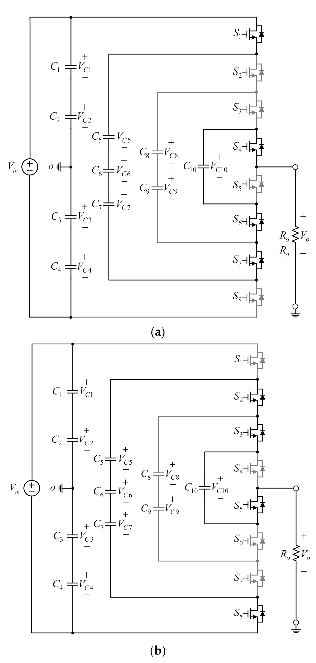
3.3.1. Switched-Capacitor-Based MLIs

The inverter presented by [30] can be considered as three modules. Module 1, called the single-pole switched capacitor (SPSC) circuit, consists of the switches S3 and S4, the capacitor C3, and the diode D. Module 2, called the second-type active-clamp switched capacitor (ACSC) circuit, consists of the switches S5, S6, S7, and S8, and the capacitors C1 and C2, where the switches S7 and S8 are used to keep the voltages on the capacitors C1 and C2 clamped to the input voltage Vin. Module 3, called the totem pole half-bridge (TPHB) circuit, is controlled by the switches S1 and S2 and operated in slow mode. These three modules use DC voltage as the SPSC input source, and ACSC and TPHB are connected in parallel to the output of the SPSC circuit to form a seven-level inverter with a voltage gain of 3.
In [31], the SC module is built up by the switches S3, S4, S5, S6, Sa and the capacitor C1. The proposed multilevel inverter is based on the switched-capacitor module with the same output characteristics as in [30] based on the SC voltage doubler unit. This inverter adopts the SC module cascaded with the three-level flywheel capacitor module and the totem pole half-bridge module and then is connected in parallel with the input source to achieve a nine-level inverter with voltage gain of 2. In addition, there are two derived circuits. One is the proposed original inverter cascaded with the SC module. The other is the proposed original inverter connected in series with the output side.
In [32], the proposed multilevel inverter is composed of the first capacitor clamping circuit based on the SC Voltage Tripler unit, the second capacitor clamping circuit based on the SC voltage doubler, and the totem pole half-bridge circuit. This multilevel inverter is similar to that in [30]. The two capacitor clamping circuits are fed by the DC voltage source, and the totem pole half-bridge circuit is connected in parallel with the output of the first capacitor clamping circuit to form a 13-level inverter with a voltage gain of 6, where the capacitor clamping voltages in these two capacitor clamping circuits are 3 times the input voltage Vin.
From the analysis mentioned above, one can see that the step switching multilevel DC-AC inverter adopts the DC power supply, semiconductor device, and capacitor to synthesize the AC output voltage. Although this inverter significantly reduces the number of switching cycles over one AC cycle, the DC-AC conversion current path is increased by too many semiconductor devices, thereby increasing conduction loss. Furthermore, since multilevel DC-AC inverters operate at low frequencies, the switched capacitors require a large capacity to provide voltage levels. In addition, the load transient response of this inverter is quite slow. For most of the capacitor clamping circuits, the capacitor charging is directly connected to the input power, and the charging will generate a huge inrush current.

3.3.2. T-Type

In [33], two conventional three-level T-type inverters are constructed as the symmetrical AC outputs, in which one cross-switched connection method is presented by using switching elements to interleave the input sources of the T-type inverter. The number of levels is increased to nine with voltage gain of 2.
In [34], another cross-connected connection method is presented, in which the corresponding circuit can be regarded as a five-level totem pole T-type inverter with a 5-fold difference in voltage magnitude between two independent input voltage sources, which is connected in series with the output end to increase the number of levels by using the voltage difference between the two input sources to achieve a 25-level inverter.
In [35], a capacitor clamping circuit consisting of a conventional three-level T-type inverter cascaded with the switches S3 to S10. By using the concept of [1], the conventional three-level T-type inverter provides input voltage levels x0 x1/2 x1, and then the cascaded clamping circuit provides voltage levels x−1 x0 x1 x2 to achieve a seven-level MLI with a voltage gain of 1.5.

3.3.3. F-Type

The research in [43] proposes a three-level F-type inverter. For a T-type inverter, the switches are placed like the letter T, and for an F-type inverter, the switches are placed like the letter F. By analyzing the loss distribution of the three-level T-type inverter, the positions of the power elements (e.g., the letter F) can be changed to reduce the voltage on some power elements during the turn-off period, which in turn reduces the switching loss of the power elements.
In [36], the three-level F-type inverter is used to increase the number of levels and voltage gain. The three-level F-type inverter is connected to a totem pole half-bridge module to boost the MLI to a five-level with a voltage gain of 1.

3.3.4. K-Type

In [37], the first K-type circuit is a three-level ANPC circuit with a floating capacitor added, in which two voltage dividing capacitors divide the neutral voltage, and then two power components are connected to this floating capacitor. In [37], the proposed topology is a five-level K-type inverter, which is finally upgraded to a seven-level K-type inverter by adding a totem pole module.
The inverter proposed in [38] is derived from the second K-type circuit. This circuit is based on an ACSC circuit. The main difference in the circuit between [38] and [37] is that in [38], the switches are placed like the letter K, so such a circuit is named K-Type. From the output manner, this circuit is also called the SC Half-mode unit. In addition, the study in [37] uses a continuous cascade manner to increase the voltage gain of the K-type.

3.3.5. Class-D-Type

The circuit presented by the study in [39] is based on an anti-noise Class-D amplifier for DC/AC power conversion, applied to 110 Vrms/60 Hz AC output with output power of less than 500 W, where this circuit can be used as a seven-level MLI with a voltage gain of 3. The proposed topology is a single-power symmetrical structure that uses an ACSC circuit to boost the voltage gain combined with a DNPC circuit for switching between levels. In particular, the control strategy focuses on improving efficiency, and the circuit structure can be designed to reduce the switching loss by only switching a single switch so as to achieve the switching level.
The research in [40] follows the DC-AC conversion application of the study [39]. The study in [39] focuses on the control strategy and DNPC structure to reduce the overall switching loss, while the research in [40] focuses on reducing the number of switches and the conduction loss. Both [39,40] are designed to maintain a circuit structure where only a single switch is switched to reach the switching level, but the proposed topology in [40] is a T-type structure modified from the DNPC of [39].

3.4. Diode-Clamped

In [10], the DNPC and T-type are combined in an asymmetric topology for the single-source AC output, where the DNPC has lower conduction loss for fast switching control and the T-type has lower switching loss for slow switching control to improve the inverter efficiency.
In [41], a full-bridge single-phase NPC structure is proposed to extend the traditional 3L-NPC to a 4L-NPC, where the full bridge refers to the 4L-NPC as a symmetric structure to provide the input voltage level x0 missing in the 4L-NPC and to enhance the overall multilevel inverter voltage gain. The neutral voltage of the conventional 3L-NPC is divided by two strings of capacitors, and its neutral voltage will change due to the change of load current, while the neutral voltage of 4L-NPC is divided by a factor of 3 of the input voltage for each of three high-capacitance capacitors, and its load current affects the neutral voltage more than 3L-NPC. It is necessary to consider the current compensation for the voltage across the voltage-divided capacitor.
The purpose of reference [42] is to increase the number of voltage levels and the output voltage gain of the inverter. The circuit can be considered as two 3L-NPC inverters with series output, where the front NPC circuit outputs to the rear neutral point of two voltage-divided capacitors. The voltage divider is converted to a clamping circuit by connecting the voltage-divided capacitor with a diode, and the rear capacitor is increased and clamped by a factor of 1.5 of the input voltage and clamped to achieve a single-phase seven-level NPC inverter with a voltage gain of 1.5.
Generally, the NP voltage of the intermediate DC-link capacitors in the diode-clamped MLI are balanced by proper operation. As the DC-AC stage has no NP balancing capability, the NP voltage has to be balanced by a preceding DC-DC stage, so the series connection of switches is allowed to avoid the complex problem of DC-link capacitor voltage balancing.

3.5. Comparison of the Recent Proposed MLIs

A comparison of the recent papers presented for the voltage-fed single-phase MLIs [10,20,21,22,23,24,25,26,27,29,30,31,32,33,34,35,36,37,38,39,40,41,42] under various criteria and feature emphases is tabulated in Table 2. In Table 3, the full names for all the abbreviations are as follows.

4. Puzzles

From the above analysis, one can see that many researchers have focused on the structure, efficiency, and output of the multilevel inverter, but comparatively few researchers have focused on the THD and product usefulness. Here, some puzzles are presented for further thinking.
(1)
THD reduction and circuit symmetry, along with two-end output and self-balancing ability, should be investigated simultaneously. As a result, not only the interchangeability of mass production but also linear control can be easily achieved. Two-end output exhibits improved linearity, as the even harmonics of the switching frequency are very effectively suppressed in a perfectly symmetrical structure. Another advantage of a balanced configuration is that the supply voltage can be halved [53].
(2)
At present, there is no standard of the input voltage. Therefore, by taking 12 V as a base, a multiple of this base to obtain 24 V, 48 V, and 96 V, depending on customer needs.
(3)
Some special structures can reduce the number of switches, but they cannot be extended to the N-level.
(4)
Modeling and advanced control should be developed. To control the switching power converter, modeling is quite important, although there are numerous variations in analysis and measurement from the perspective of theory and implementation, respectively [54]. There are many strategies presented for modeling of the DC-DC converter, for example, the well-known state-space averaging method. However, very few examples of modeling of the multilevel DC-AC inverter can be found in the literature, and only open-loop waveforms are demonstrated in many studies. That is to say, transient responses are not taken into account. Consequently, modeling of the multilevel inverter and design of the closed-loop controller should be investigated.

5. Conclusions

Multilevel converters have been extensively developed over the last two decades and show several important advantages of power electronic circuits, such as operation at high voltages, harmonics reduction, higher efficiency, modularity, smaller size, and lower cost. Now, more and more commercial products are based on the multilevel inverter structure, and more and more worldwide research and development of multilevel-inverter-related technologies are in progress. This paper has provided a brief summary of multilevel inverter circuit topologies. Although this paper cannot cover or refer to all the related work, the fundamental principles of different multilevel inverters have been introduced systematically. Not only are the recent works surveyed, but some puzzles for MLIs are also pointed out to explore new ideas and pose new questions. The research and design engineer who possesses this perspective will be the freest and most able to venture into multilevel inverter technologies.

Author Contributions

Conceptualization, J.-J.S. and K.-I.H.; methodology, J.-J.S.; software, S.-J.C.; validation, S.-J.C., K.-I.H. and J.-J.S.; formal analysis, S.-J.C.; investigation, J.-J.S.; resources, S.-J.C.; data curation, J.-J.S.; writing—original draft preparation, K.-I.H.; writing—review and editing, K.-I.H.; visualization, J.-J.S.; supervision, K.-I.H.; project administration, K.-I.H.; funding acquisition, K.-I.H. All authors have read and agreed to the published version of the manuscript.

Funding

This research was funded by the Ministry of Science and Technology, Taiwan, under the Grant Number: MOST 110-2221-E-027-045-MY2.

Data Availability Statement

Not applicable.

Conflicts of Interest

The authors declare no conflict of interest.

References

  1. Sen, P.; Jha, V.; Sahoo, A.K. Inrush current minimization in reduced device count multilevel inverter interfacing PV system. In Proceedings of the IEEE International Conference on Energy, Power and Environment: Towards Clean Energy Technologies, Shillong, Meghalaya, India, 5–7 March 2021; pp. 1–6. [Google Scholar]
  2. Wang, Y.; Shi, W.W.; Xie, N.; Wang, C.M. Diode-free T-type three-level neutral-point-clamped inverter for low-voltage renewable energy system. IEEE Trans. Ind. Electron. 2014, 61, 6168–6174. [Google Scholar] [CrossRef]
  3. Dhanamjayulu, C.; Khasim, S.R.; Padmanaban, S.; Arunkumar, G.; Holm-Nielsen, J.B.; Blaabjerg, F. Design and implementation of multilevel inverters for fuel cell energy conversion system. IEEE Access 2020, 8, 183690–183707. [Google Scholar] [CrossRef]
  4. Benedetti, D.; Agnelli, J.; Gagliardi, A.; Dini, P.; Saponara, S. Design of an off-grid photovoltaic carport for a full electric vehicle recharging. In Proceedings of the IEEE EEEIC/I&CPS Europe’20, Madrid, Spain, 9–12 June 2020; pp. 1–6. [Google Scholar]
  5. Dini, P.; Saponara, S. Electro-thermal model-based design of bidirectional on-board chargers in hybrid and full electric vehicles. Electronics 2022, 11, 112. [Google Scholar] [CrossRef]
  6. Rasool, H.; Verbrugge, B.; Zhaksylyk, A.; Tran, T.M.; El Baghdadi, M.; Geury, T.; Hegazy, O. Design optimization and electrothermal modeling of an off-board charging system for electric bus applications. IEEE Access 2021, 9, 84501–84519. [Google Scholar] [CrossRef]
  7. Vratislav, M. Three-level PWM floating H-bridge sinewave power inverter for high-voltage and high-efficiency applications. IEEE Trans. Power Electron. 2016, 31, 4065–4074. [Google Scholar]
  8. Maki, K.; Sbragio, R.; Vlahopoulos, N. System design of a wind turbine using a multi-level optimization approach. Renew. Energy 2012, 43, 101–110. [Google Scholar] [CrossRef]
  9. Wu, F.; Li, X.; Feng, F.; Gooi, H.B. Modified cascaded multilevel grid-connected inverter to enhance European efficiency and several extended topologies. IEEE Trans. Ind. Inform. 2015, 11, 1358–1365. [Google Scholar] [CrossRef]
  10. Choi, U.-M.; Lee, J.-S. Single-phase five-level IT-type NPC inverter with improved efficiency and reliability in photovoltaic systems. IEEE J. Emerg. Sel. Top. Power Electron. 2022, 10, 5226–5239. [Google Scholar] [CrossRef]
  11. Anjali Krishna, R.; Suresh, L.P. A brief review on multilevel inverter topologies. In Proceedings of the International Conference on Circuit, Power and Computing Technologies [ICCPCT], Nagercoil, India, 18–19 March 2016; pp. 1–6. [Google Scholar]
  12. Arbune, P.A.; Gaikwad, A. Comparative study of three level and five level inverter. Int. J. Adv. Res. Electr. Electron. Instrum. Eng. 2016, 5, 681–686. [Google Scholar]
  13. Rodriguez, J.; Lai, J.-S.; Peng, F.Z. Multilevel inverters: A survey of topologies, controls, and applications. IEEE Trans. Ind. Electron. 2002, 49, 724–738. [Google Scholar] [CrossRef] [Green Version]
  14. Wang, K.; Zheng, Z.; Li, Y.; Liu, K.; Shang, J. Neutral-point potential balancing of a five-level active neutral-point-clamped inverter. IEEE Trans. Ind. Electron. 2013, 60, 1907–1918. [Google Scholar] [CrossRef]
  15. Nabae, A.; Takahashi, I.; Akagi, H. A new neutral-point-clamped PWM inverter. IEEE Trans. Ind. Appl. 1981, IA-17, 518–523. [Google Scholar] [CrossRef]
  16. Sato, Y.; Natori, K. Design consideration of flying capacitor multilevel inverters using SiC MOSFETs. In Proceedings of the International Power Electronics Conference, Niigata, Japan, 20–24 May 2018; pp. 1860–1865. [Google Scholar]
  17. Naderi, R.; Sadigh, A.K.; Smedley, K.M. Dual flying capacitor active-neutral-point-clamped multilevel converter. IEEE Trans. Power Electron. 2016, 31, 6476–6484. [Google Scholar] [CrossRef]
  18. Rabinovici, R.; Baimel, D.; Tomasik, J.; Zuckerberger, A. Generic phase shifted PWM algorithm for thirteen level cascaded H-bridge NPC inverter. In Proceedings of the IEEE 26th Convention of Electrical and Electronics Engineers, Eilat, Israel, 17–20 November 2010; pp. 315–319. [Google Scholar]
  19. Babaei, E.; Laali, S.; Alilu, S. Cascaded multilevel inverter with series connection of novel H-bridge basic units. IEEE Trans. Ind. Electron. 2014, 61, 6664–6671. [Google Scholar] [CrossRef]
  20. Rao, B.N.; Suresh, Y. A novel single source multilevel inverter with hybrid switching technique. Int. J. Circuit Theory Appl. 2021, 50, 794–811. [Google Scholar]
  21. Barah, S.S.; Behera, S. An optimize configuration of H-bridge multilevel inverter. In Proceedings of the 1st International Conference on Power Electronics and Energy (ICPEE), Bhubaneswar, India, 2–3 January 2021; pp. 1–4. [Google Scholar]
  22. Kumar, N.K.; Muthyala, U.R.; Dhabale, A. Optimized multilevel inverters derived from generalized asymmetrical topology. In Proceedings of the IEEE 4th International Future Energy Electronics Conference (IFEEC), Singapore, 25–28 November 2019; pp. 1–6. [Google Scholar]
  23. Ye, M.; Wei, Q.; Li, S.; Ren, W.; Song, G. Research on balance control strategy of single capacitor clamped. IET Power Electron. 2021, 14, 280–289. [Google Scholar] [CrossRef]
  24. Missula, J.V.; Adda, R.; Tripathy, P. Averaged modeling and SRF-based closed-loop control of single-phase ANPC inverter. IEEE Trans. Power Electron. 2021, 36, 13839–13854. [Google Scholar] [CrossRef]
  25. Sun, R.; Wang, X.; Ye, Y. Seventeen-level inverter based on switched-capacitor and flying-capacitor-fed T-type unit. IEEE Access 2022, 10, 33561–33570. [Google Scholar] [CrossRef]
  26. Chen, S.; Ye, Y.; Wang, X. Hybrid 17-level inverters based on T-type flying-capacitor and switched-capacitor. Int. J. Circuit Theory Appl. 2021, 50, 886–903. [Google Scholar] [CrossRef]
  27. Lee, S.S.; Yang, Y.; Siwakoti, Y.P. A novel single-stage five-level common-ground-boost-type active neutral-point-clamped 5L-CGBT-ANPC inverter. IEEE Trans. Power Electron. 2021, 36, 6192–6196. [Google Scholar] [CrossRef]
  28. Zhang, L.; Lou, X.; Li, C.; Wu, F.; Gu, Y.; Chen, G.; Xu, D. Evaluation of different Si SiC hybrid three-level active NPC inverters for high power density. IEEE Trans. Power Electron. 2020, 35, 8224–8236. [Google Scholar] [CrossRef]
  29. Lee, S.S.; Lim, C.S.; Lee, K.-B. Novel active-neutral-point-clamped inverters with improved voltage-boosting capability. IEEE Trans. Power Electron. 2020, 35, 5978–5986. [Google Scholar] [CrossRef]
  30. Yarlagadda, A.K.; Verma, V. Seven-level triple boost self-balanced switched-capacitor inverter. Int. J. Circuit Theory Appl. 2022, 1–17. [Google Scholar] [CrossRef]
  31. Naik, B.S.; Suresh, Y.; Venkataramanaiah, J. Experimental verification of a hybrid multilevel inverter with voltage-boosting ability. Int. J. Circuit Theory Appl. 2020, 48, 420–434. [Google Scholar] [CrossRef]
  32. Ye, Y.; Zhangm, G.; Wangm, X.; Yi, Y.; Cheng, K.W.E. Self-balanced switched-capacitor thirteen-level inverters with reduced capacitors count. IEEE Trans. Ind. Electron. 2022, 69, 14827–14837. [Google Scholar] [CrossRef]
  33. Meraj; Tanzim, S.; Kamrul, H.; Ammar, M. A novel configuration of cross-switched T-type CT-type multilevel inverter. IEEE Trans. On. Power Electron. 2020, 35, 3688–3696. [Google Scholar] [CrossRef]
  34. Prem, P.; Sugavanam, V.; Abubakar, A.I.; Ali, J.S.M.; Sengodan, B.C.; Krishnasamy, V.; Padmanaban, S. A novel cross-connected multilevel inverter topology for higher number of voltage levels with reduced switch count. Int. Trans. Electr. Energy Syst. 2020, 30, e12381. [Google Scholar] [CrossRef]
  35. Lee, S.S.; Lee, K.-B. Dual-T-type seven-level boost active-neutral-point-camped inverter. IEEE Trans. Power Electron. 2019, 34, 6031–6035. [Google Scholar] [CrossRef]
  36. Bogineni, J.; Nakka, J. A novel reduced switch single-phase five-level inverter. Int. J. Circuit Theory Appl. 2022, 50, 2793–2809. [Google Scholar] [CrossRef]
  37. Sathik, M.J.; Sandeep, N.; Almakhles, D.; Blaabjerg, F. Improved “K” type seven-level switched capacitor inverter topology with self-voltage balancing. Int. J. Circuit Theory Appl. 2020, 48, 1800–1819. [Google Scholar] [CrossRef]
  38. Zeng, J.; Lin, W.; Cen, D.; Liu, J. Novel K-type multilevel inverter with reduced components and self-balance. IEEE J. Emerg. Sel. Top. Power Electron. 2020, 8, 4343–4354. [Google Scholar] [CrossRef]
  39. Shieh, J.-J.; Hwu, K.-I.; Li, Y.-Y. A single-voltage-source class-D boost multi-level inverter with self-balanced capacitors. Energies 2022, 15, 4082. [Google Scholar] [CrossRef]
  40. Shieh, J.-J.; Hwu, K.-I.; Li, Y.-Y. Analysis and modeling of a single-power-source T-Type 7-level single-phase DC-AC inverter with voltage gain of 3. Energies 2022, 15, 7894. [Google Scholar] [CrossRef]
  41. Stala, R. Natural DC-link voltage balance in a single-phase NPC inverter with four-level legs and novel modulation method. IET Power Electron. 2020, 13, 3764–3776. [Google Scholar] [CrossRef]
  42. Martinez-Garcia, M.F.; Vazquez-Guzman, G.; Martinez-Rodriguez, P.R.; Escobar, G.; Valdez-Fernandez, A.A.; Sosa-Zuniga, J.M. Step-Up seven-level neutral-point-clamped inverter based topology for TL-PVS. IET Power Electron. 2020, 13, 2847–2853. [Google Scholar]
  43. Odeh, C.I.; Lewicki, A.; Morawiec, M.; Kondratenko, D. Three-level F-type inverter. IEEE Trans. Power Electron. 2021, 36, 11265–11275. [Google Scholar] [CrossRef]
  44. Tolbert, L.M.; Habetler, T.G. Novel multi-level inverter carrier based PWM methods. IEEE Trans. Ind. Appl. 1999, 35, 1424–1431. [Google Scholar] [CrossRef] [Green Version]
  45. Chitra, U.C.; Arun, R. Bus clamping PWM for three level neutral point clamped inverters. In Proceedings of the International Conference on Technological Advancements in Power and Energy (TAP Energy), Kollam, India, 24–26 June 2015; pp. 322–326. [Google Scholar]
  46. Khluabwannarat, P.; Thammarat, C.; Tadsuan, S.; Bunjongjit, S. An analysis of iron loss supplied by sinusoidal square wave bipolar PWM inverter and unipolar PWM inverter. In Proceedings of the International Power Engineering Conference (IPEC), Singapore, 3–6 December 2007; pp. 1185–1190. [Google Scholar]
  47. Sarker, R. Phase disposition PWM (PD-PWM) technique to minimize THD from a three-phase NPC multilevel voltage source inverter. In Proceedings of the IEEE International Conference for Convergence in Engineering, Kolkata, India, 5–6 September 2020; pp. 220–224. [Google Scholar]
  48. Wang, G.; Li, Y.W. Parabolic PWM for current control of voltage-source converters (VSCs). IEEE Trans. Ind. Electron. 2010, 57, 3491–3496. [Google Scholar] [CrossRef]
  49. Sarkar, I.; Fernandes, B.G. Modified hybrid multi-carrier PWM technique for cascaded H-bridge multilevel inverter. In Proceedings of the 40th Annual Conference of the IEEE Industrial Electronics Society (IECON), Dallas, TX, USA, 29 October–1 November 2014; pp. 4318–4324. [Google Scholar]
  50. Babkrani, Y.; Naddam, A.; Hayani, S.; Hilal, M.; Fahli, A. Simulation of cascaded H-bridge multilevel inverter with several multicarrier waveforms and implemented with PD, POD and APOD Techniques. In Proceedings of the International Renewable and Sustainable Energy Conference (IRSEC), Tangier, Morocco, 4–7 December 2017; pp. 1–6. [Google Scholar]
  51. Carrara, G.; Gardella, S.; Marchesoni, M.; Salutar, R.; Sciutto, G. A new multilevel PWM method: A theoretical analysis. IEEE Trans. Power Electron. 1992, 7, 497–505. [Google Scholar] [CrossRef]
  52. Rai, S.K.; Chaturvedi, P.; Shimi, S.L. SHE-PWM based multilevel T-type inverter topology for single-phase photovoltaic applications. In Proceedings of the IEEE International Conference on Power Electronics, Drives and Energy Systems (PEDES), Trivandrum, India, 14–17 December 2016; pp. 1–4. [Google Scholar]
  53. Doutreloigne, J. A new mlti-level switching amplifier architecture with improved power efficiency. In Proceedings of the World Congress on Engineering and Computer Science (WCECS), San Francisco, CA, USA, 21–23 October 2015; pp. 1–5. [Google Scholar]
  54. Erickson, R.W.; Maksimovic, D. Fundamental Power Electronics, 2nd ed.; Electronic Services: Boulder, CO, USA, 2001. [Google Scholar]
Figure 1. Voltage-fed DC-AC inverter classification.
Energies 16 00898 g001
Figure 2. Circuit structure of a five-level neutral point clamped inverter.
Energies 16 00898 g002
Figure 3. Zero voltage output of a five-level neutral point clamped inverter.
Energies 16 00898 g003
Figure 4. (a) Current flow direction of 0.5 Vin voltage output; (b) current flow direction of −0.5 Vin voltage output.
Energies 16 00898 g004
Figure 5. (a) Current flow direction of 0.25 Vin output voltage; (b) current flow direction of −0.25 Vin voltage output.
Energies 16 00898 g005
Figure 6. Circuit structure of a five-level flywheel capacitor inverter.
Energies 16 00898 g006
Figure 7. (a) one zero voltage output; (b) the other zero voltage output of a five-level flywheel capacitor inverter.
Energies 16 00898 g007
Figure 8. (a) Current flow direction of 0.5 Vin voltage output; (b) current flow direction of −0.5 Vin voltage output.
Energies 16 00898 g008
Figure 9. (a) Current flow direction of 0.25 Vin voltage output; (b) current flow direction of 0.25 Vin voltage output.
Energies 16 00898 g009
Figure 10. Circuit structure of a five-level series-connected inverter.
Energies 16 00898 g010
Figure 11. Zero voltage output of a five-level series-connected inverter.
Energies 16 00898 g011
Figure 12. (a) Current flow direction of Vin voltage output; (b) Current flow direction of −Vin voltage output.
Energies 16 00898 g012
Figure 13. (a) Current flow direction of 2 Vin voltage output; (b) current flow direction of 2 Vin voltage output.
Energies 16 00898 g013
Table 1. Switching status and output voltage of the systematic five-level MLIs (1: ON; 0: OFF).
Inverter TypeLevel VoltageS1S2S3S4S5S6S7S8
Diode Clamped0.5 Vin11110000
0.25 Vin01111000
0 Vin00111100
−0.25 Vin00011110
−0.5 Vin00001111
Flywheel Capacitor0.5 Vin11110000
0.25 Vin11010100
0 Vin01101001
0 Vin10010110
−0.25 Vin00101011
−0.5 Vin00001111
Series-Connected2 Vin10011001
Vin00011001
000000000
Vin01100100
−2 Vin01100110
Table 2. Comparison of the recent papers presented for the voltage-fed single-phase MLIs.
[10][20][21][22][23][24]
Number of Levels595955
Number of Switches81061068
Number of Diodes200000
Number of Capacitors240013
Number of Transformers020000
Voltage Gain0.7822410.5
Number of DC Power Sources112411
End of Outputtwotwotwotwotwotwo
Rated Load Power (W)1000---------25300
Input Voltage (V)40050------24128
Peak Output Voltage (V)311100------21.664
Rated Load THD (%)---12.5017.668.9033.273.86
Peak Efficiency (%)97.0995.77------95.21---
Control StrategyUP-PWM/
OLC-PWM
PD-PWM/
TPCS
PD-PWMPD-PWMPS-PWMPS-PWM/ PD-PWM
Modelingxxxxxv
Feedback Controller Designxxxxxv
[25][26][27][28][30][31]
Number of Levels171751179
Number of Switches9117121011
Number of Diodes200010
Number of Capacitors422332
Number of Transformers000000
Voltage Gain22102.532
Number of DC Power Sources111111
End of Outputtwotwosinglesingletwotwo
Rated Load Power (W)48048040050060330
Input Voltage (V)160160401003050
Peak Output Voltage (V)32032040025084.5100
Rated Load THD (%)---6.9635.11---5.3013.51
Peak Efficiency (%)98.3697.8097.5096.6797.6197.30
Control StrategyAPOD-PWMAOD-PWMSPWMSPWMLS-PWMPD-PWM
Modelingxxxxxx
Feedback Controller Designxxxxxx
[32][33][34][35][36][37]
Number of Levels13925757
Number of Switches1010121068
Number of Diodes200005
Number of Capacitors444423
Number of Transformers000000
Voltage Gain62---1.511.5
Number of DC Power Sources122111
End of Outputtwotwotwosingletwotwo
Rated Load Power (W)500---37013012501500
Input Voltage (V)606010 V + 50 V100350200
Peak Output Voltage (V)36012060150350300
Rated Load THD (%)---9.363.26---1.55---
Peak Efficiency (%)97.3298.94---98.2098.7096.60
Control StrategyPD-PWM/SHE-PWMPD-PWMSHE-PWMPD-PWMPD-PWM
Modelingxxxxxx
Feedback Controller Designxxxxxx
[38][39][40][41][42]
Number of Levels137777
Number of Switches141210128
Number of Diodes08686
Number of Capacitors34434
Number of Transformers00000
Voltage Gain1.53311.5
Number of DC Power Sources11111
End of Outputtwotwotwotwoone
Rated-load Power (W)10003003001200100
Input Voltage (V)2605656400180
Peak Output Voltage (V)390168168400270
Rated Load THD (%)5.302.753.36---21.09
Peak Efficiency (%)96.8097.9097.4296.8095.39
Control StrategyPD-PWMLS-SPWMLS-SPWMSPWMLS-PWM
Modelingxxvxx
Feedback Controller Designxxvxx
Table 3. Abbreviations of control strategy terminologies.
NumberAbbreviationFull Name
1SPWMSinusoidal Pulse Width Modulation [44]
2OLC-PWMOne-Leg Clamping-PWM [45]
3UP-PWMUnipolar-PWM [46]
4PD-PWMPhase Disposition-PWM [47]
5TPCSTriangle and Parabolic Carrier Signals [48]
6PS-PWMPhase-Shifted-PWM [49]
7APOD-PWMAlternate Opposition Disposition-PWM [50]
8LS-PWMLevel-Shifted-PWM [51]
9SHE-PWMSelected Harmonic Elimination-PWM [52]
Disclaimer/Publisher’s Note: The statements, opinions and data contained in all publications are solely those of the individual author(s) and contributor(s) and not of MDPI and/or the editor(s). MDPI and/or the editor(s) disclaim responsibility for any injury to people or property resulting from any ideas, methods, instructions or products referred to in the content.

