Review

A Comparative Review of Three Different Power Inverters for DC–AC Applications

1
Electronic and Electrical Engineering Department, Strathclyde University, 16 Richmond St., Glasgow G1 1XQ, UK
2
School of Computing, Engineering and the Built Environment (SCEBE), Glasgow Caledonian University, 70 Cowcaddens Rd., Glasgow G4 0BA, UK
*
Author to whom correspondence should be addressed.
Energies 2023, 16(21), 7254; https://doi.org/10.3390/en16217254
Submission received: 14 August 2023 / Revised: 17 October 2023 / Accepted: 23 October 2023 / Published: 25 October 2023
(This article belongs to the Section F3: Power Electronics)

Abstract

:
This paper presents a comparative review of three different widely used power inverters, namely the conventional six-switch inverter; the reduced switch count four-switch inverter; and the eight-switch inverter. The later inverter can be reconfigured as a neutral-point diode-clamped inverter at the failure of one inverter leg. The three power inverters are compared and discussed with respect to cost, complexity, losses, common mode voltage, and control techniques. The paper is intended to serve as a guide regarding selecting the appropriate inverter for each specific application. Simulation results are presented to demonstrate the performance of the three power inverters, followed by a comprehensive comparison between the three power inverters.

1. Introduction

A DC–AC power inverter is a key component in the electrical power system. Adjustable speed drives [1], uninterruptible power supplies [2], active power filtering [3], electric vehicles [4], and the integration of renewable energy generation in power systems [5] are some areas where DC–AC inverters are deployed.
Conventionally, the six-switch (B6) inverter is utilized [6,7,8,9,10,11,12]. However, interest has increased in utilizing inverters with higher efficiency, better performance, and lower costs. In so doing, a four-switch (B4) inverter was proposed by Broeck and Wyk in 1984 [13], where one inverter leg is replaced by two DC link series tapped capacitors, hence reducing the power switches from six to four.
B4 inverters have been deployed in a wide range of applications, including three-phase [14,15] and two-phase [16] induction motor drives, brushless DC [17] and AC [18] motor drives, permanent magnet synchronous motor drives [19,20], synchronous reluctance motor drives [21], doubly fed induction generators [22], shunt active power filters [23], and grid-connected applications [24].
Reducing the number of power switches results in a more robust and reliable inverter with a low computational burden on the controller side. In addition, the number of gate drives along with interfacing circuitry is reduced [25]. It is claimed that reducing the number of switching devices from six to four reduces the cost of the converter along with decreasing the switching and conduction losses, thereby increasing inverter efficiency [26].
Since one inverter leg is removed, one phase must be connected to the center point of the two DC side series capacitors. This connection results in capacitor voltage imbalance, requiring high DC capacitance—leading to increased inverter costs and the utilization of undesirable (low-reliability) electrolytic capacitors [27].
However, DC link voltage utilization is reduced to 50% even when space vector modulation (SVM) is utilized [28]. Additionally, the available switch (states) combinations are reduced from eight (in B6 inverter) to four (in B4 inverter) without a zero-voltage vector [29].
To maintain the same output voltage, the DC link voltage must be doubled. Increasing the DC link side voltage dictates the use of switching devices with higher ratings [30]. Moreover, for adjustable speed drives, an increase in stress on motor winding is expected as a result of raising the DC link voltage [31]. Additionally, switching losses depend on the voltage, hence an increase in switching losses may be expected despite using fewer switches.
Higher-voltage-rated power semiconductor devices not only implies slower responses with lower overall efficiency but also higher costs and greater size [32]. Thus, multilevel inverters, particularly neutral-point diode-clamped inverters (NPC), become a viable solution [33]. Typically, multilevel inverters are used in medium-voltage high-power applications [34]. They offer lower voltage harmonics along with less electromagnetic interference. In addition, lower-voltage-rated switches are used hence reducing dv/dt [35].
The eight-switch (B8) inverter, which emerged as the post-fault reconfiguration of the conventional NPC inverter, is considered a potentially cost-effective inverter [36,37]. Compared with the B6 inverter, the B8 inverter has the merit of offering three-level operation, only with two extra switches [38,39], and hence better performance with an expected slightly higher cost.
On the other hand, the B8 inverter utilizes eight switches, which is double the number of power semiconductors in the B4 inverter; however, lower-voltage-rated switches are deployed [40,41]. Hence, the B8 inverter allows a series connection of fast, low-voltage, and efficient switches, but with the penalty of an increased number of gate drives and clamping diodes [42,43]. Increasing the number of switches in the B8 inverter results in nine different voltage vectors as opposed to four voltage vectors in the B4 inverter. Importantly, a zero-voltage vector is available in the B8 inverter (being particularly useful for common mode voltage control) which is absent in the B4 inverter [44,45,46,47].
There has not been any assessments comparing the performance of the B8 with the B6 inverter or with the B4 inverter. Furthermore, there is no thorough comparison between the B4 and B6 inverters. This paper presents a comprehensive comparative review to assess the performance and cost of three power inverters, namely the B6, B4, and B8 inverters, for applications below ≈3.3 kV ac.
This paper is organized as follows: Section 2 sheds light on the operation of the conventional six-switch (B6) inverter. Section 3 studies the reduced-cost four-switch (B4) inverter, highlighting the available voltage vectors, SVM operation, and the generation of zero voltage vector. Section 4 considers the NPC eight switch (B8) inverter illustrating its configuration, operation, and control. A comprehensive comparison between the three inverters is presented in Section 5, along with guidelines to properly select a suitable power inverter based on the application. Finally, conclusions and suggestions for future research are given in Section 6 and Section 7, respectively.

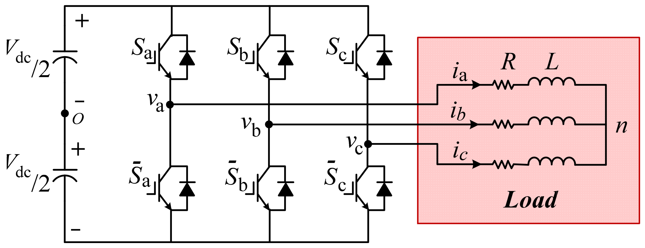
2. Six Switch (B6) Inverter

Figure 1 shows the circuit diagram of a conventional six-switch, or the B6, inverter.
The two series switches in each leg are normally complementary, at least so that no two series switches are on simultaneously, to avoid a DC supply short circuit.
The balanced three-phase voltages v a n ,   v b n ,   v c n are described via (1):
v x n = v x o v o n
where x represents the phase (a, b, and c).
The inverter voltage with respect to the reference, o, is as follows:
v x o = 2 S x 1 V d c 2
with S x representing the state of the switch; 1 is for the ON state and 0 is for the OFF state.
Therefore, from (1) and (2), v o n (which represents the common mode voltage, CMV) is defined via the following:
v o n = 1 3 v a o + v b o + v c o
Combining (1)–(3), the balanced three-phase load voltages in matrix form are given via (4):
v a n v b n v c n = 2 3 1 3 1 3 1 3 2 3 1 3 1 3 1 3 2 3 S a S b S c V d c
Generally, SVM is utilized to control the switches, thus generating the required balanced three-phase load voltages. SVM maximizes DC link voltage utilization, and also has lower switching losses and total harmonic distortion than those in conventional sinusoidal pulse width modulation.
To implement the SVM control approach, the three-phase voltages in abc co-ordinates are transformed into a two-phase αβ co-ordinate system using Clarke’s transformation, which is described via (5):
v α v β = 2 3 1 1 2 1 2 0 1 2 3 1 2 3 v a n v b n v c n
where the factor 2 3 is used to maintain constant output voltage magnitude.
The magnitude of the reference voltage along with its angle are defined via (6) and (7), respectively:
v r e f = v α 2 + v β 2
θ = tan 1 v β v α
The B6 inverter has eight switch states (six active states and two zero states) which are utilized to generate the required balanced three-phase load voltages. Figure 2 shows the active switch states along with the voltage sectors, while Table 1 summarizes the output of the eight possible switch combinations along with the corresponding CMV.
The three-phase balanced voltages are represented by a rotating vector when transformed to the space vector domain. Hence, the required balanced three-phase load voltages are transformed from abc co-ordinates into αβ co-ordinates via (5) and then represented by a rotating vector using (6) and (7). Depending on the location of the reference voltage, the sector is determined and hence the proper switch states are deployed. The reference voltage is synthesized using two adjacent active voltage vectors and the two zero vectors.
To determine the time of each switch state, the volt second equation, defined by (8), must be satisfied.
v r e f T s = v x T x + v y T y + v 0 T 0
where T s is the sampling time, v x and v y represent the two adjacent active vectors, with times T x and T y respectively, while v 0 represents the zero vector with time T 0 . The switch times T x , T y , and T 0 are defined via (9)–(11), respectively:
T x = 3 T s v r e f V d c sin 60 ° m θ
T y = 3 T s v r e f V d c sin θ 60 ° m 1
T 0 = T s T x T y
where m is the sector
Table 2 summarizes the switch times for switches S a , S b , and S c , where these times are compared with a carrier signal of amplitude, T s , to generate the required gating pulses.
From Figure 2 (according to the radius of the largest circle inscribed in the hexagon), the maximum output phase voltage (in the linear modulation region) which can be synthesized using SVM for the B6 inverter is Vdc/√3.

3. Four Switch (B4) Inverter

The four-switch (B4) inverter only has two semiconductor legs (each containing two complementary switches), while the conventional third leg is replaced with a split DC capacitor as illustrated in Figure 3.
Since one of the phases (phase ‘a’ for example) is connected to the mid-point of the split DC capacitor, its voltage is fixed to zero, as defined via (12):
v a o = 0
While phases b and c voltages with respect to the reference, o, are given via (13):
v x o = 2 S x 1 V d c 2
The balanced three-phase load voltages in matrix form are given via (14):
v a n v b n v c n = 2 3 1 3 1 3 1 3 2 3 1 3 1 3 1 3 2 3 1 2 S b S c V d c
The B4 inverter only has two sectors with four active switch states without any zero states. Figure 4 shows the four available switch states along with the voltage sectors.
Table 3 summarizes the output of the four possible switch combinations and the different CMVs.
Depending on the location of the reference voltage, the sector is determined and hence the proper switch states are deployed. The reference voltage is synthesized using three active vectors (where two opposite vectors are used to generate the missing zero state).
For operation in sector one, the three vectors V 2 , V 1 , and V 3 are utilized with the switch times T 2 , T 1 , and T 3 defined via (15)–(17), respectively:
T 2 = 3 v r e f V d c T s sin θ
T 1 = T s 2 1 T 2 T s + 3 v r e f V d c cos θ
T 3 = T s T 1 T 2
On the other hand, when the reference voltage vector is in sector two, the switch times T 4 , T 1 , and T 3 for the vectors V 4 , V 1 , and V 3 are given by (18)–(20), respectively:
T 4 = 3 v r e f V d c T s sin θ
T 1 = T s 2 1 T 4 T s + 3 v r e f V d c cos θ
T 3 = T s T 1 T 4
Table 4 summarizes the switch times for S b and S c .
From Figure 4, the maximum output phase voltage (in the linear modulation region) which can be synthesized using SVM for the B4 inverter is V d c 2 3 .

4. Eight Switch (B8) Inverter

The eight-switch (B8) inverter (which is the post-fault reconfiguration of the three-level NPC inverter) is shown in Figure 5.
The B8 inverter has two legs with four switches in each leg. Switches S x 1 and S x 3 , and S x 2 and S x 4 are complementary. Phase a is connected to the mid-point of the split DC capacitor; hence, its voltage is fixed as given via (21):
v a o = 0
Phases b and c voltages with respect to the reference, o, are given via (22):
v x o = S x 1 + S x 2 1 V d c 2
The balanced three-phase load voltages are given via (23):
v a n v b n v c n = 2 3 1 3 1 3 1 3 2 3 1 3 1 3 1 3 2 3 1 S b 1 + S b 2 S c 1 + S c 2 V d c 2
The B8 inverter has nine different switch states (eight active states and one zero state) which are utilized to generate the required balanced three-phase load voltages. Table 5 summarizes the output of the eight possible switch combinations along with the generated CMV.
The eight active switch states are divided into six short vectors and two medium vectors, hence two possible SVM approaches are available. However, utilizing the six active short vectors and avoiding the two active medium vectors gives better performance than does utilizing the eight active vectors [47].
Figure 6 shows the eight active switch states along with the six voltage sectors.
Depending on the location of the reference voltage, the sector is determined and hence the proper switch states are deployed. The reference voltage is synthesized using two adjacent active short voltage vectors and the zero vector.
The switch times T x , T y , and T 0 , representing the times of the two adjacent active short vectors and the zero vector respectively, are defined via (24)–(26):
T x = 2 3 T s v r e f V d c sin 60 ° m θ
T y = 2 3 T s v r e f V d c sin θ 60 ° m 1
T 0 = T s T x T y
The times calculated in (24)–(26) are similar to those of the B6 inverter except for the multiplication by a factor of two (this is due to the reduction in DC link utilization as will be illustrated later). Furthermore, the switch time of the zero vector is achieved using the only available zero state for the B8 inverter. But two zero vectors are available for the B6 inverter which are both utilized to generate the zero-voltage state.
Table 6 summarizes the switch times for switches S b 1 , S b 2 , S c 1 , and S c 2 .
The maximum output phase voltage (in the linear modulation region) which can be synthesized using SVM for the B6 inverter is Vdc/2√3.

5. Comparison between the B6, B4, and B8 Inverters

This section presents a comprehensive comparison between the three inverters, viz the conventional six-switch (B6) inverter, the reduced switch count four-switch (B4) inverter, and the eight-switch (B8) NPC inverter. The comparison covers aspects including DC link voltage utilization, switch ratings, losses, cost, and performance. Table 7 illustrates the parameters of the simulation model. The Simulink model for the B4 inverter, as an example, is illustrated in Appendix A. Results are demonstrated in Figure 7.
The DC link voltage of the B6 inverter is 600 V since the DC link voltage utilization of the B4 and the B8 inverters is half that for the B6 inverter. Therefore, a 1200 V DC link is utilized for the B4 and the B8 inverters to attain the same output voltage. Figure 7a shows the three-phase load currents for the three inverters, where B6 has the best current quality with 2.38% total harmonic distortion (THD). However, using a 1200 V DC link voltage for the B4 inverter increases the THD to 5.95%. Introducing a three-level operation for the B8 inverter reduces the THD to 3.41% (which is still higher than that of the B6 inverter as a result of the need to double the DC link voltage). Figure 7b shows the harmonic content for the three inverters, while Figure 7c shows the pole voltage for the three inverters. The voltage harmonic spectrum is demonstrated in Figure 7d. Investigating the voltage harmonic spectrum is crucial to identify which harmonic order has the highest magnitude. This guides the designer in selecting the appropriate passive filter in grid-connected applications [48].
Since CMV is an important factor [49,50] for three-phase inverters (particular when feeding electrical machines), it is highlighted in Figure 7e. The B6 inverter has a CMV of ± 1 2 V d c . Since the DC link voltage is 600 V for the B6 inverter, the CMV is ± 300   V . The CMV for the B4 and the B8 inverters is ± 1 3 V d c , specifically ± 400 V, since the DC link voltage is doubled.
The performance of the three inverters is investigated at half the load given in Table 7 with the results in Figure 8. Balanced three-phase currents are achieved with the three inverters as shown in Figure 8a. The current harmonic content is demonstrated in Figure 8b. As expected, reducing the load (while maintaining the same switching frequency) increases the THD. However, still, the B6 inverter has the lowest THD, at 4.57%, followed by the B8 inverter, at 6.54% and finally, the B4 inverter with the highest THD, at 11.48%. Phase voltage is shown in Figure 8c with the voltage harmonics illustrated in Figure 8d. Finally, CMV is highlighted in Figure 8e.
For a comprehensive comparison, the switching losses and conduction losses of the three inverters must be assessed [51,52]. Table 8 illustrates the main specifications of the utilized power switches. All switches are IXYZ—the same technology.
The power MOSFET conduction loss is as follows:
P c o n d = I D , r m s 2 R D S o n
where R D S o n is the drain-source on-state resistance and I D , r m s is the load rms current.
The conduction loss can be calculated using the drain-source on-state resistance which is obtained from the datasheet, as in Table 8 with the B4 inverter utilizing four 1200 V switches. The B6 and B8 inverters utilize six and eight 600 V switches, respectively. Using (27), and for the same rms current, the conduction losses of the B4 and B8 inverters with respect to the B6 inverter are 1.56 and 1.33, respectively.
Switching losses arise during switch turn on/off, where the losses depend on the drain-source voltage ( V D S ), load current (   I D ), switching frequency ( f s ), and the turn-on/off times ( t o n ,   t o f f , respectively) (losses in clamping diodes are neglected as fast Schottky devices are deployed).
Equation (28) defines the switching losses assuming a linear voltage/current switching behavior.
P s w = V D S   I D t o n + t o f f 6   f s
For the same switching frequency and load current, the switching losses of the B4 and B8 inverters with respect to the B6 inverter are in the ratio of 3.3:1 and 1.33:1, respectively. Since the B8 inverter uses the same switch ratings as the B6 inverter, a 33% increase in the switching and conduction losses is expected as a result of requiring two extra switches (neglecting losses in clamping diodes as fast Schottky devices can be deployed), while the B4 inverter requires fewer switches. However, the increase in the switch voltage rating results in an increase in switching and conduction losses.
Converter efficiency is calculated as follows:
η = o u t p u t   p o w e r o u t p u t   p o w e r + l o s s e s × 100 %
The three inverters feed a 13.5 kW load. Based on (27)–(29), the efficiencies of the B6, B8, and B4 inverters are 97.0%, 96.1%, and 95.5%, respectively. This reveals that the B6 inverter has the best efficiency, followed by the B8 inverter, with the B4 inverter coming last. This is expected as the B4 inverter has the highest switching and conduction losses as a result of deploying slow, higher-voltage power semiconductor devices. Subsequently, the B4 inverter requires a larger heat sink followed by B8 and finally the B6 inverter.
To extend the inverter performance study, Figure 9 investigates the efficiency and THD at different power levels.
Figure 9a shows the efficiency at different converter output powers. At low output power levels, the switching and conduction losses are minimal as the load current is reduced, hence the efficiency is high. Increasing the load power results in an increase in current and thereby switching and conduction losses result in efficiency degradation. Furthermore, Figure 9a reveals that at all power levels the B6 inverter has the highest efficiency, while the B4 has the lowest.
Since THD is an important performance aspect, Figure 9b studies the variation in THD for the three inverters at different output power levels with the same switching frequency. As expected, the B6 inverter has the best performance with the lowest THD, followed by the B8 inverter, and then the B4 inverter. All the results are at the same switching frequency, for a valid comparison. At light loads with low currents, the THD increases as expected.
The previous results presented the performance of the three inverters when feeding a static RL load, so to further investigate inverter performance, a dynamic load is required. An induction motor (IM), with the parameters in Table 9, is used as the dynamic load. The switching frequency is the same as that for previous results (2.75 kHz).
The performance of the three inverters is demonstrated in Figure 10. The three-phase stator currents are shown in Figure 10a from the instant of IM starting until the steady state. Direct on-line starting is applied, which justifies the high starting current. The current harmonic spectrum is illustrated in Figure 10b. As expected, the B6 inverter has the lowest THD, at 2.57%, while the B4 inverter recorded the lowest THD, at 6.22%. The three-level operation of the B8 inverter improves the THD to 3.66%, compared to the B4 inverter; however, its performance is not better than that of the B6 inverter due to the higher DC link voltage.
All the previous results are obtained at the same low switching frequency (2.75 kHz). In order to illustrate the switching frequency effect on inverter performance, the IM load, with the parameters in Table 9, is fed from the three inverters operating at a 5 kHz switching frequency. Results are seen in Figure 11.
Balanced three-phase stator currents are achieved in the steady state by the three inverters, as shown in Figure 11a. Increasing the switching frequency improves the current quality as highlighted in Figure 11b, where a reduction in THD is recorded for all the three inverters, when a 5 kHz switching frequency is deployed as opposed to that of 2.75 kHz. The results are given in Figure 10. Additionally, as expected, the B6 inverter still offers the best performance with the lowest THD among the three inverters at 1.41%, followed by the B8 inverter, at 2.01%, and finally the B4 inverter, at 3.42%.
For critical applications, reliability is of prime importance [53]. Reliability could be defined as the ability of a component to function properly for a period of time without failure. In power inverters, semiconductor devices and particularly DC link electrolytic capacitors are items prone to failure. Electrolytic-type capacitors tend to be avoided, at the expense of increased costs. Due to the switching and conduction losses in power semiconductor devices, where energy is dissipated in the form of heat, a rise in junction temperature is expected. The variation in junction temperature leads to thermomechanical stress which can result in device failure. Furthermore, gate drive circuit failure will result in converter malfunction. With the B8 inverter being composed of eight power switches, four clamping diodes and eight gate drivers, the probability of converter failure is higher. On the other hand, the B4 inverter has only four power switches and gate drivers; hence, it has the highest reliability among the three inverters from the power semiconductor device’s point of view.
Since the B4 inverter operates with a DC link voltage that is twice that of a corresponding B6/B8 inverter, the voltage rating of B4 power semiconductor devices is higher, resulting in higher switching and conduction losses. If the generated heat energy is not efficiently dissipated via the proper selection of switches, and heat sink design, the B4 inverter will be more prone to failure.
On the other hand, both the B4 and B8 inverters connect one of the phases to the center point of the DC link capacitor, resulting in capacitor voltage ripple. This capacitor voltage ripple (hence current ripple) suggests that B4 and B8 DC link capacitors are more prone to failure than is the B6 inverter capacitor.
Generally, four approaches could be implemented to improve power inverter reliability, specifically utilizing robust components in a better-cooled environment, continuous monitoring and control, utilizing advanced power semiconductor devices, specifically wide-bandgap GaN and SiC devices, and finally increasing inverter redundancy by utilizing extras switches to reconfigure the inverter in case of switch failure.
Table 10 gives a comprehensive comparison between B6, B4, and B8 inverters.
Figure 12 summarizes the comparison between the B6, B4, and B8 inverters in terms of seven aspects, namely cost effectiveness, compactness, converter simplicity, computational speed, efficiency, THD, and CMV. Each aspect is scaled from 1 to 10.

6. Conclusions

This paper presented a comprehensive comparison between three types of widely deployed power inverters used in lower-voltage applications (<3.3 kV ac); namely, the six-switch (B6) inverter, the reduced-switch-count (B4) inverter, and the eight-switch NPC (B8) inverter. The comparison covered aspects including circuit diagram, operation, SVM techniques, semiconductor device rating, switching and conduction losses, output current THD, and the complexity of the inverters. It is concluded that the B6 inverter is superior in performance, which justifies its wide deployment in applications including high-power variable speed drives, renewable energy systems, electric vehicles, and active power filters. The B4 inverter is suitable for low-power applications where a compact and simple inverter is required. Typical applications for the B4 inverter include domestic home appliances, heating, ventilation and air-conditioning systems (HVAC), uninterruptable power supplies (UPS), micro-grid interfaces, photo-voltaic (PV) cells, motion control systems, and electric bikes.
Finally, the B8 inverter is seen to not be a suitable option in any application as it is complex, expensive, and has low performance (even with the presence of three-level operation due to the increase in DC link voltage) when compared with that of the B4 (compact inverter) and B6 (high-performance) inverter. Therefore, the B8 inverter is only suitable as a post-fault reconfiguration of the NPC inverter or possibly at voltage levels just beyond those suitable for the other two inverters (where other multi-series switch configurations become applicable).

7. Future Research

In order to extend the inverter operating range and improve the voltage utilization factor, overmodulation techniques are proposed and studied in detail in the literature for the conventional six-switch B6 inverter. However, overmodulation techniques have not been extensively investigated for the four-switch (B4) and eight-switch (B8) inverters. Enhancing the output voltage of the B4 inverter, which is suitable for applications requiring compact-size inverters, is beneficial to extending the operating range of the inverter. From another perspective, the B4 inverter switch voltage rating could be reduced (while maintaining the same output voltage by operating in the overmodulation region), resulting in a reduction in losses, hence an increase in inverter efficiency.
Furthermore, in the past decades there has been increased interest in the use of renewable energy resources. The use of inverters is inevitable for grid connection, resulting in harmonics being injected into the grid. The passive filter design has been investigated for the conventional B6 inverter. However, there has not been any research reported on the design of passive filters for the B4 and B8 inverters.
Finally, this paper presented a comprehensive comparison and evaluation of B6, B4, and B8 converters when deployed for DC–AC inverter applications. The research could be extended and generalized to compare the three converters when used for other applications, like AC–DC rectification (active front end rectifiers) and harmonic elimination, as shunt active power filters.

Author Contributions

Conceptualization, A.A.-A. and M.A.E.; analysis, A.A.-A.; methodology, A.A.-A., M.A.E. and B.W.; software, A.A.-A.; supervision, B.W.; writing—review and editing, A.A.-A., M.A.E. and B.W. All authors have read and agreed to the published version of the manuscript.

Funding

This research received no external funding.

Data Availability Statement

The data presented in this study are available in Appendix A and Appendix B.

Conflicts of Interest

The authors declare no conflict of interest.

Appendix A

The MATLAB/Simulink model for the B4 inverter is illustrated in Figure A1.
Figure A1. B4 MATLAB/Simulink model.
Energies 16 07254 g0a1
The required three-phase reference voltage is generated using sinusoidal sources.
Figure A2. Sector determination.
Energies 16 07254 g0a2
Figure A3. B4 PWM.
Figure A3. B4 PWM.
Energies 16 07254 g0a3
Figure A4. B4 inverter.
Energies 16 07254 g0a4
The balanced three-phase voltage is transformed using a Clarke transformation block (abc to αβ) as given via (5). The magnitude and phase are then extracted as defined via (6) and (7). Figure A2 shows the process of sector determination, where the phase is checked to determine if the reference vector is in sector 1 or 2. Based on the sector, an m-file MATLAB function block is used to determine the vector times as given via (15)–(20). Additionally, the switching times are then calculated as illustrated in Table 4. A copy of the m-file code is presented in Appendix B. A PWM block, as demonstrated in Figure A3, is deployed to generate the required gating signals. Considering a VSC, two switches in a leg are complementary; hence, the inversion of the upper switches’ gate signal is evident. The switching times calculated via the function block are compared against a sawtooth signal. The generated gating signals control the B4 inverter switches shown in Figure A4. The B4 inverter is built using built-in Simulink IGBT/diode blocks.
The B6 and B8 inverters are simulated using the above detailed approach, but with the corresponding equations and circuit configuration.

Appendix B

MATLAB code:
function [Tphb, Tphc]= fcn(Vref,angle,sector,Vdc,Ts)
 
  
if sector==1
      T2=sqrt(3)*Vref/Vdc*Ts*sind(angle);
      T1=Ts/2*(1-T2/Ts+3*Vref/Vdc*cosd(angle));
      T3=Ts-T1-T2;
      T4=0;
          Tphb=T2+T3;
          Tphc=T3;
else
      T4=-sqrt(3)*Vref/Vdc*Ts*sind(angle);
      T1=Ts/2*(1-T4/Ts+3*Vref/Vdc*cosd(angle));
      T3=Ts-T1-T4;
      T2=0;
          Tphb=T3;
          Tphc=T4+T3;
end

References

  1. Rauber, A.; den Bakker, P. A Comparison of Adjustable-Speed Drive Systems: Voltage Source Inverters and Load-Commutated Inverters for High-Power Applications. IEEE Ind. Appl. Mag. 2020, 26, 56–66. [Google Scholar] [CrossRef]
  2. Singh, Y.; Singh, B.; Mishra, S. An Uninterruptable PV Array-Battery Based System Operating in Different Power Modes with Enhanced Power Quality. IEEE Trans. Ind. Electron. 2022, 69, 3631–3642. [Google Scholar] [CrossRef]
  3. Kukrer, O.; Komurcugil, H.; Guzman, R.; de Vicuna, L.G. A New Control Strategy for Three-Phase Shunt Active Power Filters Based on FIR Prediction. IEEE Trans. Ind. Electron. 2021, 68, 7702–7713. [Google Scholar] [CrossRef]
  4. Bai, H.K.; Costinett, D.; Tolbert, L.M.; Qin, R.; Zhu, L.; Liang, Z.; Huang, Y. Charging Electric Vehicle Batteries: Wired and Wireless Power Transfer: Exploring EV charging technologies. IEEE Power Electron. Mag. 2022, 9, 14–29. [Google Scholar] [CrossRef]
  5. Tuckey, A.; Round, S. Grid-Forming Inverters for Grid-Connected Microgrids: Developing “good citizens” to ensure the continued flow of stable, reliable power. IEEE Electrif. Mag. 2022, 10, 39–51. [Google Scholar] [CrossRef]
  6. Flota-Bañuelos, M.; Miranda-Vidales, H.; Fernández, B.; Ricalde, L.J.; Basam, A.; Medina, J. Harmonic Compensation via Grid-Tied Three-Phase Inverter with Variable Structure I&I Observer-Based Control Scheme. Energies 2022, 15, 6419. [Google Scholar] [CrossRef]
  7. Huang, K.-H.; Chao, K.-H.; Sun, Z.-Y.; Ho, C.-Y. Design and Implementation of Three-Phase Smart Inverter of the Photovoltaic Power Generation Systems. Appl. Sci. 2023, 13, 294. [Google Scholar] [CrossRef]
  8. Tawfiq, K.B.; Mansour, A.S.; Sergeant, P. Mathematical Design and Analysis of Three-Phase Inverters: Different Wide Bandgap Semiconductor Technologies and DC-Link Capacitor Selection. Mathematics 2023, 11, 2137. [Google Scholar] [CrossRef]
  9. Ali, A.I.M.; Takeshita, T.; Sayed, M.A. Three-Phase PWM Inverter for Isolated Grid-Connected Renewable Energy Applications. Energies 2021, 14, 3701. [Google Scholar] [CrossRef]
  10. Alathamneh, M.; Ghanayem, H.; Yang, X.; Nelms, R.M. Three-Phase Grid-Connected Inverter Power Control under Unbalanced Grid Conditions Using a Time-Domain Symmetrical Components Extraction Method. Energies 2022, 15, 6936. [Google Scholar] [CrossRef]
  11. Fu, Y.; Ji, Y.; Meng, G.; Chen, W.; Bai, X. Three-Phase Inverter Fault Diagnosis Based on an Improved Deep Residual Network. Electronics 2023, 12, 3460. [Google Scholar] [CrossRef]
  12. Alathamneh, M.; Ghanayem, H.; Yang, X.; Nelms, R.M. Three-Phase Grid-Connected Inverter Power Control under Unbalanced Grid Conditions Using a Proportional-Resonant Control Method. Energies 2022, 15, 7051. [Google Scholar] [CrossRef]
  13. Van Der Broeck, H.W.; Van Wyk, J.D. A Comparative Investigation of a Three-Phase Induction Machine Drive with a Component Minimized Voltage-Fed Inverter under Different Control Options. IEEE Trans. Ind. Appl. 1984, IA-20, 309–320. [Google Scholar]
  14. Ni, K.; Hu, Y.; Liu, Y.; Gan, C. Performance Analysis of a Four-Switch Three-Phase Grid-Side Converter with Modulation Simplification in a Doubly-Fed Induction Generator-Based Wind Turbine (DFIG-WT) with Different External Disturbances. Energies 2017, 10, 706. [Google Scholar] [CrossRef]
  15. El Badsi, B.; Bouzidi, B.; Masmoudi, A. DTC Scheme for a Four-Switch Inverter-Fed Induction Motor Emulating the Six-Switch Inverter Operation. IEEE Trans. Power Electron. 2013, 28, 3528–3538. [Google Scholar] [CrossRef]
  16. Ouarda, A.; Badsi, B.E.; Masmoudi, A. Direct RFOC Strategies Aimed to Symmetrical Two-Phase IM Drives: Comparison Between B4- and B6-Inverters in the Stator. IEEE Trans. Power Electron. 2018, 33, 9772–9782. [Google Scholar] [CrossRef]
  17. Naseri, F.; Farjah, E.; Schaltz, E.; Lu, K.; Tashakor, N. Predictive Control of Low-Cost Three-Phase Four-Switch Inverter-Fed Drives for Brushless DC Motor Applications. IEEE Trans. Circuits Syst. I Regul. Pap. 2021, 68, 1308–1318. [Google Scholar] [CrossRef]
  18. Hoang, K.D.; Zhu, Z.Q.; Foster, M.P. Influence and Compensation of Inverter Voltage Drop in Direct Torque-Controlled Four-Switch Three-Phase PM Brushless AC Drives. IEEE Trans. Power Electron. 2011, 26, 2343–2357. [Google Scholar] [CrossRef]
  19. Agustin, C.A.; Yu, J.-T.; Lin, C.-K.; Jai, J.; Lai, Y.-S. Triple-Voltage-Vector Model-Free Predictive Current Control for Four-Switch Three-Phase Inverter-Fed SPMSM Based on Discrete-Space-Vector Modulation. IEEE Access 2021, 9, 60352–60363. [Google Scholar] [CrossRef]
  20. Hicham, F.; Yousfi, D.; Mohamed Larbi, E.; Youness, A.D. Four-Switch Three-Phase PMSM Converter with Output Voltage Balance and DC-Link Voltage Offset Suppression. Information 2017, 8, 11. [Google Scholar] [CrossRef]
  21. Lin, C.-K.; Agustin, C.A.; Yu, J.-T.; Cheng, Y.-S.; Chen, F.-M.; Lai, Y.-S. A Modulated Model-Free Predictive Current Control for Four-Switch Three-Phase Inverter-Fed SynRM Drive Systems. IEEE Access 2021, 9, 162984–162995. [Google Scholar] [CrossRef]
  22. Zarei, M.E.; Nicolás, C.V.; Arribas, J.R.; Ramírez, D. Four-Switch Three-Phase Operation of Grid-Side Converter of Doubly Fed Induction Generator with Three Vectors Predictive Direct Power Control Strategy. IEEE Trans. Ind. Electron. 2019, 66, 7741–7752. [Google Scholar] [CrossRef]
  23. Trinh, Q.-N.; Lee, H.-H. An Advanced Current Control Strategy for Three-Phase Shunt Active Power Filters. IEEE Trans. Ind. Electron. 2013, 60, 5400–5410. [Google Scholar] [CrossRef]
  24. Dasgupta, S.; Mohan, S.N.; Sahoo, S.K.; Panda, S.K. Application of Four-Switch-Based Three-Phase Grid-Connected Inverter to Connect Renewable Energy Source to a Generalized Unbalanced Microgrid System. IEEE Trans. Ind. Electron. 2013, 60, 1204–1215. [Google Scholar] [CrossRef]
  25. Uddin, M.N.; Radwan, T.S.; Rahman, M.A. Fuzzy-logic-controller-based cost-effective four-switch three-phase inverter-fed IPM synchronous motor drive system. IEEE Trans. Ind. Appl. 2006, 42, 21–30. [Google Scholar] [CrossRef]
  26. Zaky, M.S.; Metwaly, M.K. A Performance Investigation of a Four-Switch Three-Phase Inverter-Fed IM Drives at Low Speeds Using Fuzzy Logic and PI Controllers. IEEE Trans. Power Electron. 2017, 32, 3741–3753. [Google Scholar] [CrossRef]
  27. Sun, D.; Su, J.; Sun, C.; Nian, H. A Simplified MPFC With Capacitor Voltage Offset Suppression for the Four-Switch Three-Phase Inverter-Fed PMSM Drive. IEEE Trans. Ind. Electron. 2019, 66, 7633–7642. [Google Scholar] [CrossRef]
  28. Kim, J.; Hong, J.; Nam, K. A Current Distortion Compensation Scheme for Four-Switch Inverters. IEEE Trans. Power Electron. 2009, 24, 1032–1040. [Google Scholar]
  29. Zhou, D.; Zhao, J.; Liu, Y. Predictive Torque Control Scheme for Three-Phase Four-Switch Inverter-Fed Induction Motor Drives with DC-Link Voltages Offset Suppression. IEEE Trans. Power Electron. 2015, 30, 3309–3318. [Google Scholar] [CrossRef]
  30. Blaabjerg, F.; Neacsu, D.O.; Pedersen, J.K. Adaptive SVM to compensate DC-link voltage ripple for four-switch three-phase voltage-source inverters. IEEE Trans. Power Electron. 1999, 14, 743–752. [Google Scholar] [CrossRef]
  31. Blaabjerg, F.; Freysson, S.; Hansen, H.; Hansen, S. A new optimized space-vector modulation strategy for a component-minimized voltage source inverter. IEEE Trans. Power Electron. 1997, 12, 704–714. [Google Scholar] [CrossRef]
  32. Peng, F.; Ye, J.; Emadi, A. An asymmetric three-level neutral point diode clamped converter for switched reluctance motor drives. IEEE Trans. Power Electron. 2017, 32, 8618–8631. [Google Scholar] [CrossRef]
  33. Abdel-Aziz, A.A.; Ahmed, K.H.; Wang, S.; Massoud, A.M.; Williams, B.W. A Neutral-Point Diode-Clamped Converter with Inherent Voltage-Boosting for a Four-Phase SRM Drive. IEEE Trans. Ind. Electron. 2020, 67, 5313–5324. [Google Scholar] [CrossRef]
  34. Rodriguez, J.; Bernet, S.; Steimer, P.K.; Lizama, I.E. A Survey on Neutral-Point-Clamped Inverters. IEEE Trans. Ind. Electron. 2010, 57, 2219–2230. [Google Scholar] [CrossRef]
  35. Jayakumar, V.; Chokkalingam, B.; Munda, J.L.A. Comprehensive Review on Space Vector Modulation Techniques for Neutral Point Clamped Multi-Level Inverters. IEEE Access 2021, 9, 112104–112144. [Google Scholar] [CrossRef]
  36. Lin, B.R.; Wei, T.C. A novel NPC inverter for harmonics elimination and reactive power compensation. IEEE Trans. Power Deliv. 2004, 19, 1449–1456. [Google Scholar] [CrossRef]
  37. Lin, B.-R.; Wei, T.-C. Space vector modulation strategy for an eight-switch three-phase NPC converter. IEEE Trans. Aerosp. Electron. Syst. 2004, 40, 553–566. [Google Scholar]
  38. Ozdemir, S.; Altin, N.; Komurcugil, H.; Sefa, I. Sliding Mode Control of Three-Phase Three-Level Two-Leg NPC Inverter with LCL Filter for Distributed Generation Systems. In Proceedings of the IECON 2018—44th Annual Conference of the IEEE Industrial Electronics Society, Washington, DC, USA, 21–23 October 2018; pp. 3895–3900. [Google Scholar]
  39. Xiang, C.; Ouyang, Z.; Zhang, X.; Iu, H.H.C.; Cheng, S. An Improved Predictive Current Control of Eight Switch Three-Level Post-Fault Inverter with Common Mode Voltage Reduction. IEEE Trans. Circuits Syst. I Regul. Pap. 2022, 69, 3861–3872. [Google Scholar] [CrossRef]
  40. Deng, Q.; Ge, X.; Lin, C.; Xie, D.; Gou, B.; Feng, X. An Optimized SVPWM Strategy for the Postfault Three-Level NPC Voltage Source Inverters. IEEE Trans. Ind. Appl. 2021, 57, 6182–6194. [Google Scholar] [CrossRef]
  41. Xiang, C.; Zhang, X.; Iu, H.H.-C.; Zhang, L.; Cheng, S. Duty VV-MPTC for Post-Fault Eight Switch Three-Phase Inverter Fed Induction Motor Drives with Reduced Neutral Point Voltage Fluctuation. IEEE Trans. Power Electron. 2021, 36, 11691–11700. [Google Scholar] [CrossRef]
  42. Liu, Y.C.; Ge, X.; Feng, X.; Ding, R. Relationship between SVPWM and carrier-based PWM of eight-switch three-phase inverters. Electron. Lett. 2015, 51, 1018–1019. [Google Scholar] [CrossRef]
  43. Zhang, M.; Guo, Y.B.; Li, Z.; Zhang, X.H. Suppression strategy for output unbalance of eight switch three-phase inverter. Electron. Lett. 2017, 53, 951–953. [Google Scholar] [CrossRef]
  44. Liu, Y.; Ge, X.; Tang, Q.; Gou, B. Two modified SVPWM algorithms for common-mode voltage reduction in eight-switch three phase inverters. Electron. Lett. 2017, 53, 676–678. [Google Scholar] [CrossRef]
  45. Altin, N.; Sefa, I.; Komurcugil, H.; Ozdemir, S. A Modified Lyapunov-Function Based Control Scheme for Three-Phase Three-Level Two-Leg Grid-Tied NPC Inverter. In Proceedings of the 2019 7th International Istanbul Smart Grids and Cities Congress and Fair (ICSG), Istanbul, Turkey, 25–26 April 2019; pp. 218–222. [Google Scholar]
  46. Tang, Q.; Ge, X.; Liu, Y.C.; Hou, M. Improved switching-table-based DTC strategy for the post-fault three-level NPC inverter-fed induction motor drives. IET Elect. Power Appl. 2018, 12, 71–80. [Google Scholar] [CrossRef]
  47. Tang, Q.; Ge, X.; Liu, Y.C. Performance analysis of two different SVM-based field-oriented control schemes for eight-switch three-phase inverter-fed induction motor drives. In Proceedings of the 2016 IEEE 8th International Power Electronics and Motion Control Conference (IPEMC-ECCE Asia), Hefei, China, 22–26 May 2016; pp. 3374–3378. [Google Scholar]
  48. Ahmed, K.H.; Finney, S.J.; Williams, B.W. Passive Filter Design for Three-Phase Inverter Interfacing in Distributed Generation. In Proceedings of the 2007 Compatibility in Power Electronics, Gdansk, Poland, 29 May–1 June 2007; pp. 1–9. [Google Scholar]
  49. Khoun Jahan, H.; Eskandari, R.; Rahimi, T.; Shalchi Alishah, R.; Ding, L.; Bertilsson, K.; Sabahi, M.; Blaabjerg, F. A Limited Common-Mode Current Switched-Capacitor Multilevel Inverter Topology and Its Performance and Lifetime Evaluation in Grid-Connected Photovoltaic Applications. Energies 2021, 14, 1915. [Google Scholar] [CrossRef]
  50. Jun, E.-S.; Park, S.-y.; Kwak, S. A Comprehensive Double-Vector Approach to Alleviate Common-Mode Voltage in Three-Phase Voltage-Source Inverters with a Predictive Control Algorithm. Electronics 2019, 8, 872. [Google Scholar] [CrossRef]
  51. Graovac, D.; Purschel, M.; Kiep, A. MOSFET Power Losses Calculation Using the Data-Sheet Parameters. Infineon Appl. Note 2006, 1, 1–23. [Google Scholar]
  52. Depew, J. Efficiency Analysis of a Synchronous Buck Converter Using Microsoft Office Excel-Based Loss Calculator. Microchip Appl. Note 2012, AN1471, 1–14. [Google Scholar]
  53. Falck, J.; Felgemacher, C.; Rojko, A.; Liserre, M.; Zacharias, P. Reliability of Power Electronic Systems: An Industry Perspective. IEEE Ind. Electron. Mag. 2018, 12, 24–35. [Google Scholar] [CrossRef]
Figure 1. Six switch (B6) inverter.
Energies 16 07254 g001
Figure 2. B6 switch states.
Energies 16 07254 g002
Figure 3. Four-switch (B4) inverter.
Energies 16 07254 g003
Figure 4. B4 switch states.
Energies 16 07254 g004
Figure 5. Eight-switch (B8) inverter.
Energies 16 07254 g005
Figure 6. B8 switch states.
Energies 16 07254 g006
Figure 7. Comparison between B6, B4, and B8 inverters at full load. (a) Load currents, (b) current FFT analysis, (c) pole voltage, (d) voltage FFT analysis, and (e) CMV.
Energies 16 07254 g007aEnergies 16 07254 g007b
Figure 8. Comparison between B6, B4, and B8 inverters at half load. (a) Load currents, (b) current FFT analysis, (c) pole voltage, (d) voltage FFT analysis, and (e) CMV.
Energies 16 07254 g008
Figure 9. B6, B4, and B8 inverters’ performances at different power levels. (a) Efficiency and (b) THD.
Energies 16 07254 g009
Figure 10. Comparison between B6, B4, and B8 inverters feeding an IM load. (a) Load currents and (b) current FFT analysis.
Energies 16 07254 g010
Figure 11. Comparison between B6, B4, and B8 inverters with higher switching frequency feeding IM load: (a) load currents, and (b) current FFT analysis.
Energies 16 07254 g011
Figure 12. Converter comparison.
Energies 16 07254 g012
Table 1. B6 inverter switch states.
Vector S a S b S c v r e f θ CMV
0000 0 0 ° 1 2 V d c
1100 2 3 V d c 0 ° 1 6 V d c
2110 2 3 V d c 60 ° 1 6 V d c
3010 2 3 V d c 120 ° 1 6 V d c
4011 2 3 V d c 180 ° 1 6 V d c
5001 v V d c 240 ° 1 6 V d c
6101 2 3 V d c 300 ° 1 6 V d c
7111 0 0 ° 1 2 V d c
Table 2. B6 inverter switch times.
Sector S a S b S c
1 T x + T y + 1 2 T 0 T y + 1 2 T 0 1 2 T 0
2 T x + 1 2 T 0 T x + T y + 1 2 T 0 1 2 T 0
3 1 2 T 0 T x + T y + 1 2 T 0 T y + 1 2 T 0
4 1 2 T 0 T x + 1 2 T 0 T x + T y + 1 2 T 0
5 T y + 1 2 T 0 1 2 T 0 T x + T y + 1 2 T 0
6 T x + T y + 1 2 T 0 1 2 T 0 T x + 1 2 T 0
Table 3. B4 inverter switch states.
Vector S b S c v r e f θ CMV
100 1 3 V d c 0 ° 1 3 V d c
210 1 3 V d c 90 ° 0
311 1 3 V d c 180 ° 1 3 V d c
401 1 3 V d c 270 ° 0
Table 4. B4 inverter switch times.
Sector S b S c
1 T 2 + T 3 T 3
2 T 3 T 3 + T 4
Table 5. B8 inverter switch states.
Vector S b 1 S b 2 S c 1 S c 2 v r e f θ CMV
00101 0 0 ° 0
10000 1 3 V d c 0 ° 1 3 V d c
20100 1 3 V d c 60 ° 1 6 V d c
31100 1 3 V d c 90 ° 0
41101 1 3 V d c 120 ° 1 6 V d c
51111 1 3 V d c 180 ° 1 3 V d c
60111 1 3 V d c 240 ° 1 6 V d c
70011 1 3 V d c 270 ° 0
80001 1 3 V d c 300 ° 1 6 V d c
Table 6. B8 inverter switch times.
Sector S b 1 S b 2 S c 1 S c 2
1 T y + T 0 T 0
2 T y T x + T y + T 0 T y + T 0
3 T x + T y T x + T y + T 0 T y T x + T y + T 0
4 T x T x + T y + T 0 T x + T y T x + T y + T 0
5 T x + T 0 T x T x + T y + T 0
6 T 0 T x + T 0
Table 7. Simulation parameters.
ParameterValue
Output voltage (rms L-L)380 V
Output frequency50 Hz
Load resistance10 Ω
Load inductance10 mH
DC link capacitor5 mF
Switching frequency2.75 kHz
Table 8. Specifications of the power switches.
PointB4 InverterB6/B8 Inverter
SwitchIXFB30N120PIXFR48N60P
Voltage rating (V)1200600
Current Rating (A)3032
Turn on resistance (Ω)0.350.15
Turn on rise time (ns)6025
Turn off fall time (ns)5622
Table 9. IM parameters.
ParameterValue
Voltage (rms L-L)380 V
Frequency50 Hz
Torque50 Nm
Speed1440 rpm
Stator resistance0.6 Ω
Rotor resistance0.63 Ω
Stator leakage inductance3.5 mH
Rotor leakage inductance5.47 mH
Mutual inductance35.4 mH
Table 10. Comparison between B6, B4, and B8 inverters.
FeatureB6B4B8
DC link voltage (for same output voltage) V d c 2 V d c 2 V d c
Number of DC link capacitors222
DC link capacitor voltage 1 2 V d c V d c V d c
Number of gate drivers 648
Number of switches (and freewheel diodes)648
Switch voltage rating V d c 2 V d c V d c
Total switches, VA6   V d c I 8   V d c I 8   V d c I
Number of clamping diodes 4
Clamping diode rating V d c
Total clamping diodes, VA 4   V d c
Circuit complexityModerateLowHigh
Converter sizeModerateCompactLarge
Converter reliabilityModerateHighLow
Computational burdenModerateLowModerate
Switch states849
Switching/Conduction lossesLowHighModerate
Heat sink sizeSmallLargeMedium
THDLowHighModerate
CMVLowModerateModerate
Disclaimer/Publisher’s Note: The statements, opinions and data contained in all publications are solely those of the individual author(s) and contributor(s) and not of MDPI and/or the editor(s). MDPI and/or the editor(s) disclaim responsibility for any injury to people or property resulting from any ideas, methods, instructions or products referred to in the content.

