Article

Hardware-in-the-Loop Testing for Protective Relays Using Real Time Digital Simulator (RTDS)

1
Department of Electrical and Computer Engineering, University of Kentucky, Lexington, KY 40506, USA
2
Schweitzer Engineering Laboratories, Inc., Columbus, OH 43035, USA
*
Author to whom correspondence should be addressed.
Energies 2023, 16(3), 1039; https://doi.org/10.3390/en16031039
Submission received: 29 November 2022 / Revised: 11 January 2023 / Accepted: 13 January 2023 / Published: 17 January 2023
(This article belongs to the Special Issue Power System Analysis, Operation and Control)

Abstract

:
With the increasing size and complexity of power systems, it is crucial to have an effective protection system in place to ensure its reliability. One of the important components of the protection system are relays. It is important for a relay to operate dependably and securely so that any fault can be cleared in time to minimize damages to the power network. However, it is important to test a relay in a realistic environment before commissioning it to the network. Testing a relay in the actual network can be expensive with limited fault scenarios. Hence, Hardware-in-the-Loop (HIL) testing is an efficient method to perform closed-loop testing of a relay since numerous fault cases can be simulated to provide a realistic operating environment for the relay under test. This paper sheds light on the HIL testing done for protective relays using a sample distribution system using RTDS. Two SEL-351 relays have been used in this experiment, and proper settings for the relays are calculated for coordination. The paper also describes the procedure of configuring the relay and other RTDS components crucial for interfacing of the relay with RTDS. After test setup, a pre-fault, fault, and post-fault analysis was done for the system. The results obtained from these analyses are cross-checked with the event history of the two SEL-351 relays, obtained with AcSELerator Quickset software. This paper provides thorough information for researchers to replicate the presented study or to develop new HIL experiments. It can also help in developing a fundamental understanding of the HIL testing setup that can be further applied to a more complex power system.

1. Introduction

The power system in the modern era has evolved into large and complex interconnected systems which is composed of nonlinear and dynamic elements. The development of smart grids has led to wide-scale integration of numerous elements at different operation levels of the grid. This has created complexities in the system and operational challenges that can be resolved using real-time digital computation, and advanced sensors and communication technologies [1,2,3]. With the increased sophistication in the methods and equipment for testing, power system simulation tools can play a major role in the testing and analysis of the system.
Power system simulation methods are mainly classified in two types: offline simulation and real-time simulation. Offline simulation methods have limited ability to provide an accurate simulation for the behavior of real-life equipment and practical systems [4]. The real-time simulation technology can perform numerous complex operations on the power system as they consist of high-speed processors and can provide higher efficiency and performance. Recently, Hardware-in-the-Loop (HIL) simulation has gained popularity, as it can wedge the gap between the behavior of the simulated and real system. In HIL testing, the power system under study is represented by a simulation model on a real time simulation platform, and the equipment under test is outside of the model but is linked to the simulation model through special Digital to Analog and Analog to Digital cards and necessary sensors and amplifiers [4,5]. One of the biggest advantages of HIL is that it can reduce the risk of field errors in actual scenarios [6]. HIL testing allows for simulating a real scenario of the power system, such as a fault situation, and provides accurate data on handling such situations in the real world [7]. HIL simulation platform performs time domain simulation to generate transient waveforms that are encountered in many protection applications [8,9,10].
With the increased energy demand, it has become crucial to procure the demand in an economically and environmentally sustainable way. Due to this, the stability and safety limit of modern power grids are being pushed. To handle the surge and the pressure, utilities are adding sophisticated new schemes and devices to their networks [11]. Whenever a new equipment and controller is added to the system, it needs to be tested and tuned before adding it to the network. In this situation, HIL simulation can be used for analyzing the new equipment in the simulated model before commissioning in the field [4,5,12].
Over the years, real-time simulation has become popular among manufacturers and utilities to assist them in the study of behavior and operation of the power system, performing the closed-loop testing of new equipment, and developing new protection and control functions [11].
Out of all the functions performed by a real-time simulation system, this paper is concerned with performing closed-loop testing of directional overcurrent relays using RTDS. Closed-loop testing of equipment in a model power system can mimic the characteristics of the system in a realistic scenario. Hence, readily decipherable information can be obtained on the performance of the equipment. In closed-loop testing of the relay, the RTDS outputs voltage and currents signals that are fed to the relay, and the relay provides an output, i.e., a tripping signal to the RTDS to open the circuit breaker in the RTDS model to disconnect the faulted section, and the simulation continues with the updated model [13]. The closed loop setting is ideal for testing the coordination between multiple relays.
A directional overcurrent relay is one of the primary safety equipment used in a networked, non-radial electrical distribution system to ensure the reliable and efficient operation of the power system. This relay monitors the current flowing through the protected element and generates a trip signal to the circuit breaker in the case of an occurrence of a fault, i.e., when the current exceeds the value of pickup current in the relay [14].
Numerous studies have been conducted in the field of HIL testing. These studies have been performed for various power system equipment using different real-time simulation software. F. R. Adegbohun et al. conducted a HIL testing for a grid-connected PV system consisting of SEL-421 relay, to test the hardware compatibility and model reliability [7]. A performance analysis of relays was done by M. Afshar et al. for detection of high impedance faults using a RTDS. A 15-bus system was modeled in RSCAD with an arc model for the high impedance fault [15]. The authors of [16] proposed an improved numerical algorithm based on PSCAD/EMTDC simulation to eliminate the overreach issue in distance relay caused due to transients of the coupling capacitor voltage transformer. The authors proposed a prototype for distance relay that was tested using RTDS. The proposed relay had a faster operation speed and higher reliability. Y. S. Cho et al. designed a RSCAD model containing multi-function relay and mimic board to improve the understanding of the technology associated with the protection and operation of the power system [17]. K. H. So et al. performed a closed-loop testing for differential and distance relay using EMTP [18]. O. Dias et al. [19] and T. Ledwaba et al. [20] focused on the HIL testing of transmission network. In [19], a 500 kV Brazilian transmission network was protected using SEL-421 distance relays. The simulation was performed for two fault cases: permanent and transient faults. The results were also cross-checked with the available field data. The HIL testing using ABB RED 670, a differential relay for a 400 kV, 50 Hz transmission network was performed in [20]. They also studied the system dynamics with additional equipment, such as series capacitor. A non-linear programming based adaptive protection scheme for coordination of directional overcurrent relays in a 7-bus system was proposed in [21]. The results were validated using RTDS. Reference [22] proposed a coordination algorithm for advanced distance, and an over current relay was proposed that was validated using RTDS and Avera hardware relays. In [23], a flywheel energy storage system (FESS), a primary energy storage component of an energy magazine, was tested using a Power Hardware-in-the Loop (PHIL) simulation. A 3.5MJ, 320kW FESS was virtually interfaced with a simulated model of a shipboard. M. Stifter et al. presented a PMU-RTS-HIL testbed for validation and testing of multiple PMUs. Various HIL platforms exist, such as Opal-RT, Typhoon, and RTDS. Opal-RT was used for the aforesaid task [24]. Reference [25] illustrated recent best practices in the field of development of real-time simulator, from the perspective of RTDS.
This paper uses RTDS to perform HIL tests, and it is expected that the method is readily extendable to other real time simulation platforms. The paper provides a thorough illustration of calculating scaling factors of GTAO card of RTDS, cable connection between digital I/O cards of RTDS and low-level interface of relay, connection with power amplifiers, and consideration of amplification factor of amplifiers in calculating GTAO scaling factors. It is crucial that these tasks are performed correctly to have a successful experiment.
The rest of the paper is organized as follows: Section 2 describes the RSCAD model developed in RTDS for a five-bus system selected for this experiment. Section 3 describes the procedure to configure the SEL-351 relays before they are used for HIL testing. Section 4 explains the different relay schemes used in the HIL testing. Section 5 discusses the key components and procedures in interfacing of the relays with the RTDS. Section 6 presents the findings achieved for the work carried out in Section 2, Section 3, Section 4 and Section 5. Section 7 concludes the methodology used for this research.

2. Development of a RTDS Model for the Five-Bus System

This section describes the development of an RTDS model of a five-bus system. The model is developed in power mode. Additionally, crucial components for interfacing relays under testing conditions with the model simulated with the RTDS will be shown.

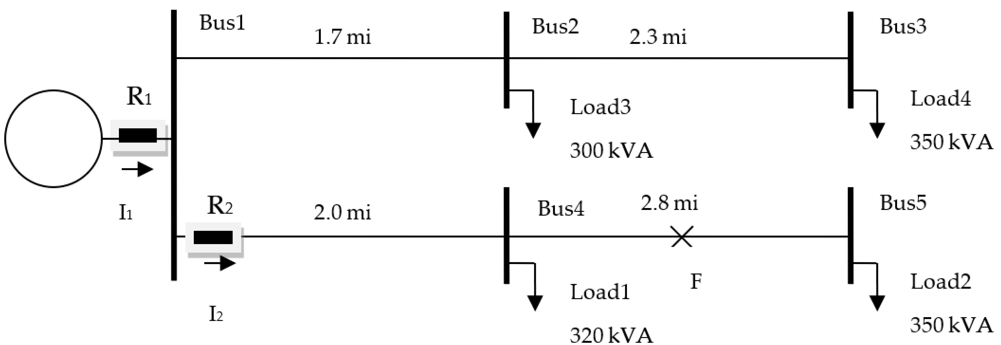
2.1. Five-Bus System

Figure 1 depicts a five-bus system considered for protection. R1 and R2 are the two SEL-351 relays (i.e., directional overcurrent relays under study). SEL-351 relays can protect lines and equipment using phase, negative sequence, residual-ground, and neutral-ground overcurrent elements with directional control. The modeled system is a sample 12.47 kV (L-L RMS) overhead power distribution system. The lengths of feeders are in miles, and the load ratings are given in kVA. A power factor of 0.9 is assumed for all the loads. A three-phase fault (F) has been introduced in the system for the relays under study.

2.2. RTDS Model

The five-bus system shown in Figure 1 has been modeled for RTDS using the RSCAD software, as shown in Figure 2 and Figure 3. The model has been divided into two modules for illustration purpose. Module 1 shows the RSCAD model developed for the five-bus system, and module 2 shows how the RTDS model interfaces with the relays. In reality, it is a single model containing both modules to perform the HIL testing.
The feeder lines shown in Figure 2 are labelled using the pi-section element in RSCAD. The feeder line impedances between each bus have been provided as input to the relevant pi-section model connecting them. A three-phase sinusoidal source of rating 12.47 kV line-to-line RMS voltage has been selected for the model. Four grounded R-L loads were connected to buses 2, 3, 4, and 5. A circuit breaker was added between source and bus 1 and another between bus 1 and bus 4. The feeder impedance matrix in ohms/mile was as follows:
  • [0.3465 + j1.0179 0.1560 + j0.5017 0.1580 + j0.4236
  • 0.1560 + j0.5017 0.3375 + j1.0478 0.1535 + j0.3849
  • 0.1580 + j0.4236 0.1535 + j0.3849 0.3414 + j1.0348].
The pre-fault rms current at R1 was 60.2 A, and fault current was 1770.0 A. The pre-fault rms current at R2 was 30.6 A, and the fault current was 1758.7 A.
The instantaneous overcurrent relay settings were calculated as follows. At R1, the tripping current was set as three times the pre-fault current: 60.2 × 3 / 120 = 1.51 A secondary, where 120:1 was the CT ratio when using a CT tapped at 600:5. The fault current will be 1770 / 120 = 14.75 A secondary.
At R2, the tripping current was set as three times the pre-fault current: 30.6 × 3 / 120 = 0.77 A secondary, where 120:1 was the CT ratio for a CT tapped at 600:5. The fault current will be 1758.7 / 120 = 14.66 A secondary, which will be used in setting the time dial for the inverse-time overcurrent protection elements, to achieve a proper coordination.

3. SEL-351 Relay Configuration

To configure the SEL-351 relay, SEL’s AcSELerator Quickset software was used. In this study, two SEL-351 relays were chosen. The configuration was done as follows. First, the communication between the computer and the relay was established. Then the as-found relay settings were read to the computer. In the ‘General settings’, the CT and PT ratio were set to 120 and 60 (12,470 / 60 = 207 V secondary L-L), respectively, for both the relays. The parameters in ‘Line Settings and Fault locator’ section, as shown in Figure 4, needed to be calculated as follows:
S e l f   i m p e d a n c e   ( Z s ) = a v e r a g e   o f   t h e   d i a g o n a l   e l e m e n t s   o f   f e e d e r   i m p e d a n c e   m a t r i x = Z 11 + Z 22 + Z 33 3
M u t u a l   i m p e d a n c e   ( Z m )         = a v e r a g e   o f   n o n         d i a g o n a l   e l e m e n t s   o f   f e e d e r   i m p e d a n c e   m a t r i x         = Z 12 + Z 21 + Z 13 + Z 31 + Z 23 + Z 32 6
Z e r o   s e q u e n c e   p r i m a r y   i m p e d a n c e   ( Z 0 p ) = Z s + ( 2 Z m )
P o s i t i v e   s e q u e n c e   p r i m a r y   i m p e d a n c e   ( Z 1 p ) = Z s Z m
Z e r o   s e q u e n c e   s e c o n d a r y   i m p e d a n c e   ( Z 0 s ) = Z 0 p C T   r a t i o P T   r a t i o
P o s i t i v e   s e q u e n c e   s e c o n d a r y   i m p e d a n c e   ( Z 1 s ) = Z 1 p C T   r a t i o P T   r a t i o
The pickup current of 50P1P level 1 in the ‘Phase Instantaneous Overcurrent Elements’ and the value of ‘67P1D level 1’ in the ‘Phase Definite-Time Overcurrent Elements’ can also be set as shown in Figure 5. Settings have been provided for R1, shown in Figure 5. R2 can be set in a similar way. The 50P1P level for R2 will be less than R1 (0.77 in this case) as R2 is supposed to act first. 67P1D level for R2 will be set to zero as R2 is operating under instantaneous overcurrent scheme.
Another setting is the Trip logic equation, which will be 67P1T, 50P1, 51PT—to be explained in later sections. The Trip logic equation for R1 and R2 was set to 51PT under the IDMT overcurrent scheme in Figure 6. For R2, 50P1 was used under the instantaneous overcurrent scheme, and 67P1T was used for R1 under the definite-time overcurrent scheme.
After entering the desired relay settings, the settings were written to the relay.

4. Relay Schemes

This paper focuses on the following three different relay schemes.

4.1. Instantaneous Overcurrent Scheme

Under this scheme, there was no intentional time delay in operation of the relay. The relay acts as soon as the current exceeds the pickup current setting of the relay. Relay R2 in this experiment works on this scheme. The results shown for relay R2 in case 1 of Section 6.2 of this paper were obtained using the aforesaid scheme. The 50P1P level 1 element in the Phase Instantaneous Overcurrent Elements was set to three times the value of the pre-fault current as calculated in Section 2.2.
The Trip Logic Equation was set to 50P1.

4.2. Definite Time Overcurrent Scheme

The relay R1 used the definite time scheme. Under this scheme, a pick-up setting was selected for the relay R1 as done in the instantaneous overcurrent scheme. In addition to the pickup setting, a time-setting was also provided for R1. When the current exceeded the pickup setting, R1 was supposed to wait for the specified time setting before it could issue the trip signal. A time delay of 4 cycles was set for R1, i.e., 67P1D level 1 in the Phase Definite-Time Overcurrent Elements was set to 4.0 cycles. The results for R1 using this scheme can be seen in case 2 of Section 6.2 of this paper.
The Trip Logic Equation was set to 67P1T.

4.3. Inverse Definite Minimum Time (IDMT) Overcurrent Scheme

In inverse time scheme, the relay operation time was inversely proportional to the fault current, i.e., a faster operation for a bigger fault current. In this paper, this scheme was applied to both R1 and R2 in addition to the aforementioned two schemes. A coordination was done between the two relays, where the protected feeder had a primary protection (R2) and secondary protection (R1).
The following steps were required to set up a coordination scheme for the relays under study:
  • Step 1—When setting up coordination, start with the device that will be closest to the fault within the zone of protection, i.e., relay R2 in this study.
  • Step 2—Select the appropriate relay settings for both relays as shown in Table 1.
  • Step 3—Calculate the operating time and time dial setting (51PTD) for both relay R1 and R2. Initially, the operating time of R2 will be calculated. The equation used to calculate the operating time is selected as per the IDMT curve (51PC) chosen for the relay. Since curve U3 has been selected for R2, the following formula (given in SEL-351’s instruction manual) will be used to calculate the operating time:
    t o p e r a t e R 2 = 51 P T D R 2 × ( 0.0963 + 3.88 ( M 2 1 ) )  
    where, M is a multiple of the pickup current setting, and 51 P T D R 2 is the time dial setting of R2. In this experiment, for R2, the value of M is 29.32 (14.66 / 0.5, where 0.5 is the pickup current setting of R2) (see Section 2.2), and the value of 51PTD is 1. Hence, the operating time of relay R2 will be as follows:
    t o p e r a t e R 2 = 1 × ( 0.0963 + 3.88 ( 29.32 2 1 ) ) = 0.101   s e c o n d s
  • Step 4—To calculate the operating time of R1, determine the operating time of R2 and a Coordination Interval (CI) between both relays. CI is required to ensure proper coordination with upstream devices (R1 in this case). It ensures that R2 has enough time to operate before R1 begins to operate.
A CI typically consists of relay/element operate time (pickup/tolerance), relay output operate time, breaker operate time, and a safety margin. Generally, CI ranges between 0.2 and 0.5 s for a distribution system. For this experiment, CI was taken as 0.3 s. Thus, the operating time of R1 was given as follows:
t o p e r a t e R 1 = t o p e r a t e R 2 + C I = 0.101 + 0.3 = 0.401   s e c o n d s
  • Step 5—Using the parameters in step 3 and 4, calculate 51PTD of R1 as follows:
    51 P T D R 1 = t o p e r a t e R 1 ( 0.0963 + 3.88 ( M 2 1 ) ) = 0.401 ( 0.0963 + 3.88 ( 14.75 2 1 ) ) = 3.51
    where M is 14.75 (14.75/1, where 1 is the pickup current setting of R1), as calculated in Section 2.2.
The IDMT curve (i.e., operating time v/s fault current for relay R1 and R2 for a U3 curve setting) can be plotted as shown in Figure 7.
Different curve types, pickups, or time dials can be chosen to adjust the curves shapes to achieve different coordination margins.

5. Interfacing Relays with RTDS

Figure 8 illustrates the setup for Hardware-in-the-Loop testing of SEL-351 relay using RTDS for the five-bus system. Figure 9 shows the functional block diagram for the HIL setup.
As it can be observed from Figure 9, two circuit breakers, CB1 and CB2, were used in the power system under study. CB1 was used for relay R1, and CB2 was used for R2. To connect both relays, R1 and R2, with RTDS, we required the Giga-Transceiver Analogue Output (GTAO) card and Gigabit-Transceiver Front Panel Interface (GTFPI) card provided in the RTDS. The GTAO provided analog signals, which could then be fed to a relay through an amplifier or through the low- level interface of the relay. In this study, we performed experiments using both the low-level interface method and CMS 356 (i.e., the amplifier). For successful implementation, one must consider the relay’s low-level interface scales, the current and potential transformer turns ratio, and the GTAO voltage and current scales. The GTAO provided the modeled system output to the relay, and when a fault was simulated, the relay sent a trip signal to the GTFPI card that in turn signaled the circuit breaker, which modified the simulation model, thus forming a closed-loop system. R1 here was to serve as a backup relay for faults within the protection zone of R2. When the fault occurs, R2 was supposed to act first to clear the fault. However, in case of failure of R2, R1 must act after a specified coordination delay, e.g., 4 cycles.
In Figure 9, the Amplifier refers to external devices, such as the Omicron CMS 356, which can convert RTDS low current and voltage signals (0–5 V rms) to higher current and voltage signals (0–5 A, 0–120 V rms) that are at the same level of actual CT and VT signals that can be fed to the tested relays’ current and voltage input terminals on the backside without using the relay’s low-level signal interface.
Section 5.1 and Section 5.2 provide a detailed description about the configuration of GTAO and GTFPI card, respectively, to perform their assigned operations shown in Figure 9.

5.1. GTAO Card

The GTAO card can be modelled in the RSCAD software using the GTAO element as shown in Figure 10. A GTAO card has 16 input ports. For our experiment, we needed 14 ports. In Figure 10, port 1 to 7 were the current and voltage inputs for relay R2, and port 8 to 14 were the current and voltage inputs for relay R1. The GTAO card took these inputs and provided analogue outputs to the relay input port. In Figure 9 and Figure 10, Ia, Ib, and Ic were the input phase currents for R2, and Ia_R1, Ib_R1, and Ic_R1 were the input phase currents for R1. In and In_R1 were the neutral currents for R2 and R1, respectively. At bus 1, ‘phase1Asamp’ (Va), ‘phase2Asamp’ (Vb) and ‘phase3Asamp’ (Vc) were the phase voltages.
The connections shown in Figure 10 were determined as per the highlighted connections given on the relay low-level test interface as shown in Figure 11. The rightmost parameter ‘IA’ given on the relay panel was considered as the connection on the input port 1 on the GTAO element shown in Figure 10 for relay R2 and so on. As observed from highlighted area in Figure 11, the first four parameters were for currents, and the rest were for voltages. Not following the given connection pattern will result in errors in values on the relay front panel.
The above-mentioned parameters were sampled using a sampling frequency of 7.68 kHz before being provided as an input to the GTAO card. This can be done using the sampler element provided in the RSCAD library as shown in Figure 12.

5.1.1. GTAO Scaling When Using Relay’s Low-Level Interface

The input parameters shown in Figure 10 needed to be scaled to a value within ±5 V before being sent as input to the GTAO card. These values were internally scaled in the GTAO element. This section discusses the process of obtaining the scaling factor for input current and voltage parameters for GTAO. When providing the output of the GTAO card to the relay, it is also important to consider the scaling factors of the relay. The scaling factors available for SEL-351 relay can be seen in Table 2. Initially, the required GTAO output voltages were calculated using the relay scaling factors, Current Transformer Ratio (CTR), and Potential Transformer Ratio (PTR). Then, these voltages were used to calculate the current and voltage scaling factors for the GTAO card.
Figure 13 shows the connection on the relay end between the GTAO card of the RTDS and relay. J1 was the terminal connector for input module of the relay, and J10 was the terminal for the processing module of the relay. J10 received the input secondary current and voltage parameters from the GTAO. After receiving the input secondary values, the processing module converted these values to primary values as per the relay scaling factor, CTR and PTR. These primary values could be verified on the relay front panel. Figure 14 shows the connection made on the GTAO card to provide output current and voltage values to the relay. The bottom most port of the card was the first output port of the card. The connections shown here were made as per the connection diagram shown in Figure 10 and Figure 11. Port 1 to 7 were the output values provided to relay R2, and port 8 to 14 were the output values provided to relay R1.
Connections shown in Figure 13 and Figure 14 were done for both relays shown in Figure 15. We also tested using the CMS 356 to power Relay R2, as shown in Figure 8.
For the relays used in this study, a scaling factor of 50 for current and 102 for voltage in the relay was adopted.

Calculating Required Voltage Output from GTAO Card for Input Current Parameters

As an example, assume a fault current of 4000 A and follow the steps given below to calculate the required output from the GTAO card.
  • Step 1—Calculate the secondary side value of the fault current. In this case, the CTR is 120 (i.e., 120:1). Therefore,
    S e c o n d a r y   r e l a y   c u r r e n t = P r i m a r y   C u r r e n t C T R = 4000 A 120 = 33.33   A
This secondary relay current is then stepped down within the relay and converted to a mV signal used by the relay’s processor based upon the scale factors shown in Table 2.
  • Step 2—To calculate the required output voltage from the GTAO card, divide the secondary current by the scaling factor of the relay. In our case, the scale was 50, as shown in Table 2. Therefore,
    G T A O   o u t p u t   f o r   c u r r e n t   ( V G O U T I ) = S e c o n d a r y   r e l a y   c u r r e n t R e l a y   c u r r e n t   s c a l e   f a c t o r = 33.33 50 = 0.67   V

Calculating Required Output from GTAO Card for Input Voltage Parameters

For a pre-fault voltage of 10 kV, the required GTAO voltage output can be calculated as shown below.
  • Step 1—Calculate the value on the secondary side of the relay by dividing fault current by PTR. In our case, the PTR was 60 (i.e., 60:1). Therefore,
    S e c o n d a r y   r e l a y   v o l t a g e = 10000 V 60 = 166.67   V
This secondary relay voltage is then stepped down within the relay to a mV signal used by the relay’s processor based upon the scale factors shown in Table 2.
  • Step 2—To calculate the required output voltage from the GTAO card, divide the secondary voltage by the scaling factor of the relay. In this case, the scale factor was 102, as shown in Table 2. Therefore,
    G T A O   o u t p u t   f o r   c u r r e n t   ( V G O U T I ) = S e c o n d a r y   r e l a y   v o l t a g e R e l a y   v o l t a g e   s c a l e   f a c t o r = 166.67 102 = 1.63 V
After obtaining the required GTAO outputs, calculate the scaling factor for the GTAO card to ensure that the above calculated GTAO outputs are obtained at the output of the GTAO card. The following formulas can be used to calculate the scaling factor for the voltage and current signal:
G T A O   o u t p u t   f o r   v o l t a g e   ( V G O U T V ) = 5 V s f 1000 × V a c t u a l   ( i n   v o l t s )
V s f = 5 V G O U T V × 1000 × V a c t u a l   ( i n   v o l t s ) = 5 1.63 1000 × 10000 = 30.6
or a more general equation is shown below that can be used to calculate V s f :
5 V s f 1000 × V a c t u a l   ( i n   v o l t s ) × S V × P T R = V a c t u a l   ( i n   v o l t s )
where S V is the relay voltage scale factor, which is 102. Therefore, we have
5 V s f × 1000 × V a c t u a l   ( i n   v o l t s ) × 102 × 60 = V a c t u a l   ( i n   v o l t s )
from which V s f can be derived
G T A O   o u t p u t   f o r   c u r r e n t   ( V G O U T I ) = 5 I s f × 1000 × I a c t u a l   ( i n   a m p e r e s )
I s f = 5 V G O U T I × 1000 × I a c t u a l   ( i n   a m p e r e s ) = 5 0.67 1000 × 4000 = 30
or a more general equation is shown below that can be used to calculate I s f :
5 I s f × 1000 × I a c t u a l   ( i n   a m p e r e s ) × S I × C T R = I a c t u a l   ( i n   a m p e r e s )
where S I is the relay current scale factor, which is 50. Therefore, we have
5 I s f × 1000 × I a c t u a l   ( i n   a m p e r e s ) × 50 × 120 = I a c t u a l   ( i n   a m p e r e s )
from which I s f can be derived.
Here, V s f and I s f are the scaling factors in the GTAO card for the voltage and current, respectively.

5.1.2. GTAO Scaling When Using CMS 356

The GTAO scaling was calculated differently when using CMS 356 in contrast with when using relay’s low-level interface.
In this study, the voltage amplification factor was 60 V/V, and the current amplification factor was 6.4 A/V for the CMS 356.
The GTAO scaling was calculated as follows. We have the following relationship between the GTAO output and the actual voltage and current:
G T A O   o u t p u t   f o r   v o l t a g e   ( V G O U T V ) = 5 V s f × 1000 × V a c t u a l
G T A O   o u t p u t   f o r   c u r r e n t   ( V G O U T I ) = 5 I s f × 1000 × I a c t u a l
The actual voltage is also expressed as:
V a c t u a l = V G O U T V × A M P V × P T R
The actual current is expressed as:
I a c t u a l = V G O U T I × A M P I × C T R
Here, PTR is Potential Transformer Ratio, and CTR is Current Transformer Ratio.
The GTAO scaling factor for voltage can be obtained by substituting Equation (3) in Equation (5).
V a c t u a l = 5 V s f × 1000 × V a c t u a l × A M P V × P T R
Therefore,
V s f = 5 × A M P V × P T R 1000
Equation (7) can be used to calculate the GTAO scaling factor for voltage.
For a PTR equal to 60 and A M P V of 60, the Vsf will be as follows:
V s f = 5 × A M P V × P T R 1000 = 5 × 60 × 60 1000 = 18
The GTAO scaling factor for current can be obtained by substituting Equation (4) in Equation (6).
I a c t u a l = 5 I s f × 1000 × I a c t u a l × A M P I × C T R
Therefore,
I s f = 5 × A M P I × C T R 1000
Equation (8) can be used to calculate the GTAO scaling factor for the current.
For a CTR equal to 120 and A M P I of 6.4, the I s f will be as follows:
I s f = 5 × A M P I × C T R 1000 = 5 × 6.4 × 120 1000 = 3.84

5.2. Obtaining Readings on the Relay Front Panel

After getting the required output from the GTAO card, to show the reading on the relay front panel, i.e., the primary side value, multiply the GTAO output by the current or potential transformer ratio and the scaling factor of the relay. In case of using relay’s low-level interface, the formulae are shown below:
R e l a y   v o l t a g e   r e a d i n g = V G O U T V × R e l a y   s c a l i n g   f a c t o r × P T R
R e l a y   c u r r e n t   r e a d i n g = V G O U T I × R e l a y   s c a l i n g   f a c t o r × C T R
Table 3 shows the voltage output and scaling factors obtained for GTAO for our experiment. The current and voltage values shown in Table 3 were the pre-fault values obtained on the relay front panel using the GTAO scales shown in the table. The calculations were verified by the actual readings on the relay.
When using CMS 356, the Relay reading would be calculated as the product of GTAO output and the CMS 356 amplification factor and the PT and CT ratio.

5.3. GTFPI Card

The GTFPI card was used to transmit the trip signal from the relay to the circuit breaker in the RSCAD model, as shown in Figure 16. The relay trip signal is transmitted from the relay to the RTDS digital interface panel, as shown in Figure 17 and Figure 18.
In Figure 16, ‘OUT 101’ and ‘OUT102’ are the trip signals from R1 and R2, respectively. ‘Inp_GTFPI’ is the input signal being provided from the GTFPI element. The input signal is a single word that can be converted into multiple logic outputs using a word/bit converter. The outputs of this converter are digital trip signals, i.e., logical outputs. These trip signals are then provided as an input to the digital interface panel provided on the front panel of RTDS, as shown in Figure 18. If there is only one trip signal, the converter is not required as only one port of the digital interface panel is needed. In the case of multiple trip signals, this converter is required as only one GTFPI element can be used in a RSCAD model, and this experiment required more than one port of the digital interface panel. Here, each port was considered as one bit. Two input ports will capture the two trip signals. Hence, two bits were obtained using the converter.
Figure 17 shows the connections done on the relay back panel for providing input signals to the digital interface panel of RTDS. It can be observed from the figure that ‘OUT101’ terminal of the relay has two connections (i.e., one for trip signal and another for ground). However, in general, the first terminal of the relay was the input signal, and the second terminal was ground, unlike the relay shown in Figure 17.
The connections coming from ‘OUT 101’ shown in Figure 17 were provided to the digital interface panel, as shown in Figure 18. As mentioned previously, two ports of the panel were used, i.e., one for relay R1 and one for relay R2. The input trip signal coming from relay was connected to the digital input channel on the panel, and the ground signal coming from relay was connected to the ground input on the panel.

5.4. Applying Faults to the System

Figure 19 shows the fault logic developed in RSCAD for the system. ‘SW1’, ‘SW2’, and ‘SW3’ were the switch elements in RSCAD, which denoted phases of the system. Each switch needed to be turned on to introduce the fault on the corresponding phase. For example, to apply a three-phase fault, all three switches must be turned on. Each fault type in RSCAD was assigned a binary value, which had a corresponding decimal value, as shown in Table 4. The three switches shown in Figure 19 were assigned a decimal value of 1, 2, and 4, respectively. The switch positions shown in Figure 19 indicate that a three-phase fault were introduced in the system. Alternatively, a three-phase fault can also be introduced by using a single switch having a decimal value of 7.
The fault can be applied to the system using the push button titled ‘ApplyFLT’ as shown in Figure 19. The duration of the fault can be determined using a slider titled ‘FDUR’. The output of this logic system was a control signal ‘FLT’, which was provided as an input control signal to the fault block in the RSCAD model.

5.5. Circuit Breaker Logic

Figure 20 shows the circuit breaker logic, where ‘XCBR1open’ and ‘XCBR1close’ were the push buttons used to open and close the circuit breaker contacts, respectively. The initial status of the breaker was ‘closed’, which was assigned a logical input of 1. ‘OUT101’ was the trip signal coming from relay R1. The first OR-gate was assigned for opening the circuit breaker and, hence, had two inputs, which were ‘XCBR1open’ and ‘OUT101’. The output of the first OR-gate served as the input ( S ) ¯ to the S-R flip flop. The second OR-gate was assigned for closing circuit breaker contacts. Since this experiment was not concerned with the reclosing of the circuit breaker after the occurrence of a fault, the control signal ‘PROTIED_Reclose_R1’ was assigned a zero value. The output of the second OR-gate served as the second input ( R ) ¯ to the flip flop. The output (Q) of the flip flop passed through a timer block, which determined the duration of the operation of the circuit braker. The final output of the circuit breaker logic for relay R1, i.e., ‘BRK_R1’, was provided as an input to the circuit breaker element assigned for R1 in the model. Similar logic was used for relay R2 with its corresponding trip signal and breaker signal.

6. Results

As shown in Figure 1, relay R1 is connected between the source and bus 1, and relay R2 is connected between bus 1 and bus 4. Thus, the phase voltages on bus 1, phase currents from the source, and the phase currents on the sending end of the feeder between bus 1 and bus 4 are of particular interest. The results have been obtained for the system for pre-fault, during fault, and post-fault period. The x-axis in Figure 21, Figure 22, Figure 23, Figure 24, Figure 25, Figure 26, Figure 27, Figure 28 and Figure 29 (excluding Figure 23) represents time in seconds, and the multiple y axes represent different signals, which have been explained in the previous sections.

6.1. Pre-Fault Period

Figure 21 depicts the waveforms for the pre-fault condition. The first y-axis shown in Figure 21 shows the sampled phase currents from source. The second y-axis denotes the sampled phase currents between bus 1 and bus 4. The third y-axis shows the status of the circuit breaker for relay R1. The initial status of the signal is ‘high’, as the circuit breaker is initially closed. The fourth y-axis shows the trip signal of relay R1, whose initial status is ‘low’ as there is no fault present in the system. Axes 5 and 6 show the circuit breaker status of relay R2 and trip signal of relay R2, respectively.
Figure 22 shows the line-neutral voltage (in kV) at bus 1 during pre-fault period. ‘phase1Asamp’, ‘phase2Asamp’, and ‘phase3Asamp’ are the sampled voltages for phase A, B, and C, respectively, at bus 1.

6.2. Fault Period (Instantaneous and Definite Time Scheme)

A three-phase fault with fault resistance of 0.1 ohms for a duration of 8 cycles has been applied to the system. The fault is applied in the runtime module of RTDS using a red push button shown in Figure 23. The switches shown in Figure 23 are used to select the fault type as explained in Section 5.4.
The waveforms have been obtained for two cases. In case 1, R2 operates to remove the fault. For case 2, R2 is in open loop, and R1 is in closed loop. Case 2 is simulating the scenario where R2 has failed to trip for the fault.
Figure 24 shows the current waveform and trip signal for case 1. The first y-axis in Figure 24 shows the phase current between source and bus 1 during the fault period. It can be observed that the fault current is very high for the fault duration. The second y-axis shows the phase currents between bus 1 and bus 4 during the fault. As R2 operates to remove this fault, the circuit breaker signal of R1 is high and trip signal of R1 is low as shown in third and fourth y-axis, respectively. Conversely, as observed from the sixth y-axis, the trip signal for R2 goes from low to high when the fault occurs, giving the command to the circuit breaker to open its contact. The fifth y-axis shows the breaker signal status for R2 switching from high to low when the trip signal for R2 goes from low to high.
Figure 25 depicts the current waveforms and trip signal for case 2. As the relay R1 operates to remove this fault, the circuit breaker signal of R2 is high, and the trip signal of R2 is low, as shown in fifth and sixth y-axis of Figure 25, respectively. As observed from the fourth y-axis, the trip signal for R1 goes from low to high when a fault occurs, giving the command to the circuit breaker to open its contact. The third y-axis shows the breaker signal status for R1 switching from high to low when the trip signal for R1 goes from low to high. It can be observed from Figure 24 and Figure 25 that when the relay sends the trip command, the circuit breaker opens immediately, but there is a small delay between opening of the circuit breaker and the current dropping to zero, which is characteristic of a real system.

6.3. Post-Fault Period

Figure 26 depicts the post-fault condition for case 1. The high-frequency components in the current waveforms are due to numerical chatter of RTDS simulation. As shown in the second y-axis in Figure 26, the post-fault values for sampled currents are approximately zero as the contacts of the circuit breaker for R2 are opened and does not reclose, as the reclose control signal has been set to zero in the circuit breaker logic. In the first y-axis, the phase source currents are reduced in comparison to the pre-fault condition as the feeder where the circuit breaker for relay R2 was deployed is now open, thus the source is now only supplying load on the remaining feeder. The trip signal of R2 remains high, and correspondingly, the status of circuit breaker of R2 is low because the breaker is still open.
Figure 27 shows the post-fault condition for case 2. In Figure 27, the trip signal of R1 remains high, and correspondingly, the status of the circuit breaker of R1 is low as the breaker is still open. Both phase currents are almost reduced to zero in this scenario as the breaker near the source is open.

6.4. Coordination between R1 and R2 (IDMT Scheme)

Given the operating times of R1 and R2 obtained in Section 4.3, the fault duration and the relay trip logic in this case has been modified from the one chosen for the instantaneous and definite time schemes. The fault duration has been changed to 0.637 s using the fault slider shown in Figure 19. The relay trip logic equation used in this case for both relays is 51PT. In the occurrence of a fault (three-phase fault in this case), R2 is supposed to act as per its operating time. In case of R2 failure, R1 will wait for the time duration specified by the coordination interval (CI) and then will act as per its operating time.
  • Case 1—When R2 operates
Figure 28 shows the waveforms when relay R2 operates to clear the fault. The first y-axis shows the phase currents between bus 1 and the source, and the second y-axis shows the phase currents between bus 1 and bus 4. When a three-phase fault occurs, the digital trip signal for R2 shown in the sixth y-axis goes from low to high, which in turn causes the circuit breaker signal for R2 on fifth y-axis to switch from high to low. It is observed that after a certain period, the trip signal again switches to a low value even though there is no reclosing performed in this experiment. It is because of the SELogic equations defined for R2 (referred to SEL-351’s instruction manual) which causes R2 to deenergize the trip output after a certain period. In the post-fault period, the phase currents between bus 1 and bus 4 shown in the second y-axis are zero as the breaker for R2 remains open. However, as seen in the first y-axis the post-fault currents between source and bus 1 are lower than the pre-fault period because even though breaker between bus 1 and bus 4 are open, the remaining feeder lines between bus 1, 2, and 3 are still operating.
  • Case 2—When R1 operates
When relay R2 fails to operate, R1 operates after specified CI to clear the fault. Figure 29 depicts the waveforms when R1 operates to clear the fault. It can be observed from Figure 29, the digital trip signal for relay R1 in the fourth y-axis switches from low to high while the trip signal of R2 still remains low as shown in the sixth y-axis. Correspondingly, the circuit breaker signal for R1 goes from high to low, shown in the third y-axis. In the post-fault period, all the phase currents between the source and bus 1 are zero as the breaker for R1 near the source remains open. In fourth y-axis, it can be observed as well that R1 is deenergized after some time, bringing the signal back to the ‘low’ state.

6.5. Relay Events

The software AcSELerator Quickset is used to retrieve the fault events from the two relays. Figure 30, Figure 31 and Figure 32 depict the current, voltage, and trip signals, respectively, from R2 during the instantaneous scheme. Figure 33, Figure 34 and Figure 35 show the current, voltage, and trip signals, respectively, from R1 during definite-time scheme. This section presents waveforms actually recorded by the relays to corroborate with RTDS simulation waveforms.
Figure 30 shows the phase currents for pre-fault, fault, and post-fault between bus1 and bus 4 obtained from relay R2 when deployed in instantaneous scheme. The pre-fault event shown in Figure 30 is similar to the pre-fault period for R2 shown in Figure 21. The fault event obtained from Figure 30 matches the fault period for R2 shown in Figure 24 and similar post-fault event can be seen in Figure 26. These observations indicate that RTDS and relays operate correctly as expected from the model.
The phase voltages seen in relay event for R2 in Figure 31 are similar to the phase voltage waveforms shown in Figure 22 which confirms the voltage waveforms obtained from RTDS.
Figure 32 shows the trip signal generated by R2 as per the specified trip logic equation. When comparing the trip signals in Figure 32 with Figure 21 and Figure 24, it can be noticed that they are similar and thus verified.
Figure 33 shows the phase currents for pre-fault, fault, and post-fault between bus1 and bus 4 obtained from relay R1 when deployed in the definite-time scheme. The pre-fault event shown in Figure 33 aligns with the pre-fault period for R1 shown in Figure 25. The fault event shown in Figure 33 matches the fault period for R1 shown in Figure 25 and similar post-fault event can be seen in Figure 27. This verifies the waveforms obtained for R1 from RTDS.
Figure 34 shows the voltages obtained at bus 1 when R1 is active. When compared with the voltage waveforms shown in Figure 22, it can be observed that they are similar, which verifies the waveforms obtained for R1 from RTDS.
The trip signal generated by R1 under definite-time scheme can be seen in Figure 35. When compared with the digital trip signals shown in Figure 21 and Figure 25, a similar operation of R1 can be observed in pre-fault and fault condition.
Figure 36 shows the phase currents recorded for R2 when deployed under IDMT scheme. When compared with the waveforms shown in Figure 28, the waveforms match, which validates the current waveforms achieved for R2 from RTDS.
Under IDMT scheme, the relay operates as per the operating time set for it while relay configuration. The relay is supposed to trip after the specified fault duration. The aforesaid functioning can be observed in Figure 37. The similar functioning can also be observed in Figure 28 where R2 operates the clear the fault using IDMT scheme. This validates the waveforms obtained for R2 under IDMT scheme.
In case when R2 fails to operate, R1 will act as per its operating time calculated in Section 4.3. Figure 38 shows the event for phase currents obtained for R1. When compared with Figure 29, similar current waveforms can be seen for R1, which validates the phase current waveforms obtained for R1 in RTDS.
Figure 39 shows the trip signal generated by R1 under IDMT scheme, which when compared with digital trip signal for R1 in Figure 29 verifies the RTDS waveforms.

7. Conclusions

Hardware-in-the-Loop (HIL) testing plays an increasingly critical role in system design and deployment. There is a lack of literature for providing guidance on how HIL tests can be setup including the connection of various HIL platform components, external power amplifiers, and the equipment under test and how critical parameters, such as scaling factors are calculated.
This paper presents the Hardware-in-the-Loop (HIL) testing done for a five-bus system. This paper thoroughly illustrates the procedure and steps for performing HIL test using RTDS platform, Omicron amplifiers, and SEL 351 protective relays as examples. Different tripping schemes including the Instantaneous overcurrent, Definite time, and Inverse Definite Minimum Time (IDMT) scheme have been implemented. The test results obtained by the testing platform RTDS and those recorded by the relays are compared, and the comparison confirms that the experiments are correct, and the testing platform and setup are suitable for testing protective relays. It is expected that the test setup is generally suitable for testing other equipment, such as power inverters, controllers, and machines, and such transients-based testing provides a realistic environment to better de-sign and test the equipment under test.
The procedure and framework presented in this paper will be useful for designing HIL experiments for research, education, and training purposes. In particular, the paper will provide guidance not only for students at universities, but also for professional engineers that intend to adopt and implement HIL tests.

Author Contributions

Conceptualization, Y.L.; Formal analysis, G.Y. and Y.L.; Funding acquisition, Y.L.; Methodology, G.Y., Y.L. and A.D.B.; Supervision, Y.L.; Validation, G.Y., Y.L. and A.D.B.; Writing—original draft, G.Y. and Y.L.; Writing—review & editing, Y.L. and A.D.B. All authors have read and agreed to the published version of the manuscript.

Funding

This research was funded by the Office of Naval Research, USA, under award number N00014-21-1-2972.

Data Availability Statement

Not applicable.

Acknowledgments

The authors would like to thank Arunprasanth Sakthivel, Heather Meiklejohn and Sachintha Kariyawasam from RTDS Technologies Inc. for providing their valuable guidance towards completing this research.

Conflicts of Interest

The authors declare no conflict of interest.

References

  1. Anderson, D.; Zhao, C.; Hauser, C.H.; Venkatasubramanian, V.; Bakken, D.E.; Bose, A. A Virtual Smart Grid. IEEE Power & Energy Magazine. February 2012, pp. 49–57. Available online: https://magazine.ieee-pes.org/january-february-2012/a-virtual-smart-grid/ (accessed on 23 October 2022).
  2. Nutaro, J. Designing power system simulators for the smart grid: Combining controls, communications, and electro-mechanical dynamics. In Proceedings of the IEEE Power and Energy Society General Meeting, Detroit, MI, USA, 24–28 July 2011. [Google Scholar] [CrossRef]
  3. McLaren, P.; Nayak, O.; Langston, J.; Steurer, M.; Sloderbeck, M.; Meeker, R.; Lin, X.; Yu, M.; Forsyth, P. Testing the ‘smarts’ in the smart T & D grid. In Proceedings of the IEEE/PES Power Systems Conference and Exposition (PSCE), Phoenix, AZ, USA, 20–23 March 2011; pp. 1–8. [Google Scholar] [CrossRef]
  4. Podmore, R.; Robinson, M.R. The role of simulators for smart grid development. IEEE Trans. Smart Grid 2010, 1, 205–212. [Google Scholar] [CrossRef]
  5. Montano, F.; Ould-Bachir, T.; David, J.P. An Evaluation of a High-Level Synthesis Approach to the FPGA-Based Submicrosecond Real-Time Simulation of Power Converters. IEEE Trans. Ind. Electron. 2018, 65, 636–644. [Google Scholar] [CrossRef]
  6. Chen, Y.; Dinavahi, V. Hardware emulation building blocks for real-time simulation of large-scale power grids. IEEE Trans. Ind. Inform. 2014, 10, 373–381. [Google Scholar] [CrossRef]
  7. Adegbohun, F.R.; Lee, K.Y. Real-time modeling, simulation and analysis of a grid connected PV system with hardware-in-loop protection. In Proceedings of the North American Power Symposium (NAPS), Morgantown, WV, USA, 17–19 September 2017. [Google Scholar] [CrossRef]
  8. Fan, W.; Liao, Y. Fault Location for Distribution Systems with Distributed Generations without Using Source Impedances. In Proceedings of the 51st North American Power Symposium (NAPS), Wichita, KS, USA, 13–15 October 2019. [Google Scholar] [CrossRef]
  9. Asbery, C.; Liao, Y. Fault Identification on Electrical Transmission Lines Using Artificial Neural Networks. Ph.D. Thesis, University of Kentucky, Lexington, KT, USA, 2022; pp. 13–14. [Google Scholar]
  10. Fan, W.; Liao, Y.; Kang, N. Optimal fault location for power distribution systems with distributed generations using synchronized measure-ments. Int. J. Emerg. Electr. Power Syst. 2020, 21, 20200093. [Google Scholar]
  11. Kuffel, R.; Forsyth, P.; Peters, C. The Role and Importance of Real Time Digital Simulation in the Development and Testing of Power System Control and Protection Equipment. IFAC-PapersOnLine 2016, 49, 178–182. [Google Scholar] [CrossRef]
  12. Tatcho, P.; Zhou, Y.; Li, H.; Liu, L. A real time digital test bed for a smart grid using RTDS. In Proceedings of the 2nd International Symposium on Power Electronics for Distributed Generation Systems (PEDG 2010), Hefei, China, 16–18 June 2010; pp. 658–661. [Google Scholar] [CrossRef]
  13. Marttila, R.J.; Dick, E.P.; Fischer, D.; Mulkins, C.S. Closed-loop testing with the real-time digital power system simulator. Electr. Power Syst. Res. 1996, 36, 181–190. [Google Scholar] [CrossRef]
  14. Mishra, P.; Pradhan, A.K.; Bajpai, P. Adaptive Relay Setting for Protection of Distribution System with Solar PV. In Proceedings of the 20th National Power Systems Conference (NPSC 2018), Tiruchirappalli, India, 14–16 December 2018; Volume 2, pp. 1–5. [Google Scholar] [CrossRef]
  15. Afshar, M.; Majidi, M.; Gashteroodkhani, O.A.; Amoli, M.E. Analyzing Performance of Relays for High Impedance Fault (HIF) Detection Using Hardware-In-The-Loop (HIL) Platform. Electr. Power Syst. Res. 2022, 209, 108027. [Google Scholar] [CrossRef]
  16. Chen, Y.; Wen, M.; Wang, Z.; Yin, X.; Peng, J.; Zhang, R. An improved numerical distance relay based on CCVT transient characteristic matching. Int. J. Electr. Power Energy Syst. 2020, 122, 106146. [Google Scholar] [CrossRef]
  17. Cho, Y.S.; Lee, C.K.; Jang, G.; Kim, T.K. Design and implementation of a real-time training environment for protective relay. Int. J. Electr. Power Energy Syst. 2010, 32, 194–209. [Google Scholar] [CrossRef]
  18. So, K.H.; Heo, J.Y.; Kim, C.H.; Aggarwal, R.K.; Kim, J.C.; Jang, G.S. An implementation of current differential relay and directional comparison relay using EMTP MODELS. Int. J. Electr. Power Energy Syst. 2006, 28, 261–272. [Google Scholar] [CrossRef]
  19. Dias, O.; Tavares, M.C.; Magrin, F. Hardware implementation and performance evaluation of the fast adaptive single-phase auto reclosing algorithm. Electr. Power Syst. Res. 2019, 168, 169–183. [Google Scholar] [CrossRef]
  20. Ledwaba, T.; Senyane, K.; Van Coller, J. Hardware-In-loop testing of a differential relay used to Protect single/double circuit transmission lines. In Proceedings of the Southern African Universities Power Engineering Conference/Robotics and Mechatronics/Pattern Recognition Association of South Africa (SAUPEC/RobMech/PRASA 2019), Bloemfontein, South Africa, 28–30 January 2019; pp. 347–352. [Google Scholar] [CrossRef]
  21. Naveen, P.; Jena, P. Directional Overcurrent Relays Coordination Scheme for Protection of Microgrid. In Proceedings of the IEEE First International Conference on Smart Technologies for Power, Energy and Control (STPEC 2020), Nagpur, India, 25–26 September 2020. [Google Scholar] [CrossRef]
  22. Singh, M.; Telukunta, V.; Srivani, S.G. Enhanced real time coordination of distance and user defined over current relays. Int. J. Electr. Power Energy Syst. 2018, 98, 430–441. [Google Scholar] [CrossRef]
  23. Langston, J.; Steurer, M.; Schoder, K.; Borraccini, J.; Dalessandro, D.; Rumney, T.; Fikse, T. Power hardware-in-The-loop simulation testing of a flywheel energy storage system for shipboard applications. In Proceedings of the IEEE Electric Ship Technologies Symposium (ESTS), Arlington, VA, USA, 14–17 August 2017; pp. 305–311. [Google Scholar] [CrossRef]
  24. Stifter, M.; Cordova, J.; Kazmi, J.; Arghandeh, R. Real-time simulation and hardware-in-the-loop testbed for distribution synchrophasor applications. Energies 2018, 11, 876. [Google Scholar] [CrossRef] [Green Version]
  25. Sidwall, K.; Forsyth, P. A Review of Recent Best Practices in the Development of Real-Time Power System Simulators from a Simulator Manufacturer’s Perspective. Energies 2022, 15, 1111. [Google Scholar] [CrossRef]
Figure 1. System considered for protection.
Energies 16 01039 g001
Figure 2. Module 1 of the RSCAD model.
Energies 16 01039 g002
Figure 3. Module 2 of the RSCAD model.
Energies 16 01039 g003
Figure 4. Entering parameters for ‘Line settings and Fault locator’ section.
Energies 16 01039 g004
Figure 5. Setting 50P1P and 67P1D level for R1.
Energies 16 01039 g005
Figure 6. Trip logic equation for R1 and R2 under IDMT scheme.
Energies 16 01039 g006
Figure 7. Relay operating time v/s Fault current for the inverse time scheme.
Energies 16 01039 g007
Figure 8. HIL setup for both SEL-351 relays, using RTDS.
Energies 16 01039 g008
Figure 9. Block diagram for HIL setup.
Energies 16 01039 g009
Figure 10. GTAO element in the RSCAD model.
Energies 16 01039 g010
Figure 11. Low–level test interface for SEL–351 relay.
Energies 16 01039 g011
Figure 12. Sampling of the parameters.
Energies 16 01039 g012
Figure 13. Connection on the relay end between relay and GTAO card.
Energies 16 01039 g013
Figure 14. Connection on the GTAO end between the relay and the GTAO card.
Energies 16 01039 g014
Figure 15. Relay R1 and R2 used for experiment.
Energies 16 01039 g015
Figure 16. GTFPI element in RSCAD.
Energies 16 01039 g016
Figure 17. Connection on relay back panel with digital interface panel of RTDS.
Energies 16 01039 g017
Figure 18. Digital interface panel of RTDS receiving signal from relay.
Energies 16 01039 g018
Figure 19. Fault logic.
Energies 16 01039 g019
Figure 20. Circuit breaker logic for relay R1.
Energies 16 01039 g020
Figure 21. Current waveforms for pre-fault condition.
Energies 16 01039 g021
Figure 22. Voltage at bus 1 preceding the fault.
Energies 16 01039 g022
Figure 23. Applying fault to the system in RTDS environment.
Energies 16 01039 g023
Figure 24. Waveforms for fault condition when R2 operates—case 1.
Energies 16 01039 g024
Figure 25. Waveforms for fault condition when R1 operates—case 2.
Energies 16 01039 g025
Figure 26. Waveforms for post-fault condition when R2 operates—case 1.
Energies 16 01039 g026
Figure 27. Waveforms for post-fault condition when R1 operates—case 2.
Energies 16 01039 g027
Figure 28. Waveforms when relay R2 operates to clear the fault.
Energies 16 01039 g028
Figure 29. Waveforms when relay R1 operates to clear the fault.
Energies 16 01039 g029
Figure 30. Phase currents recorded by R2 under instantaneous scheme.
Energies 16 01039 g030
Figure 31. Phase voltages recorded by R2 under instantaneous scheme.
Energies 16 01039 g031
Figure 32. Trip logic and trip signal recorded by R2 under instantaneous scheme.
Energies 16 01039 g032
Figure 33. Phase currents recorded by R1 under definite-time scheme.
Energies 16 01039 g033
Figure 34. Phase voltages recorded by R1 under definite-time scheme.
Energies 16 01039 g034
Figure 35. Trip logic and trip signal recorded by R1 under definite-time scheme.
Energies 16 01039 g035
Figure 36. Event obtained for phase currents recorded by R2 under IDMT scheme.
Energies 16 01039 g036
Figure 37. Trip signal generated by R2 under IDMT scheme.
Energies 16 01039 g037
Figure 38. Event obtained for phase currents recorded by R1 under IDMT scheme.
Energies 16 01039 g038
Figure 39. Trip signal generated by R1 under IDMT scheme under IDMT scheme.
Energies 16 01039 g039
Table 1. Relay settings for coordination scheme.
ParametersRelay R1Relay R2
Pickup current setting (51PP)10.5
IDMT curve (51PC)U3U3
Table 2. Scaling factors for SEL-351 relay.
Input Channels (Relay Rear Panel)Input Channel Nominal RatingInput ValueCorresponding J1 Output ValueScale Factor (Input/Output) (A/V or V/V)
IA, IB, IC, IN1 A1 A100 mV10
IA, IB, IC, IN5 A5 A100 mV50
IN0.2 A0.2 A114.1 mV1.753
IN0.05 A0.05 A50 mV1
VA, VB, VC, VS150 V67 VLN1313.7 mV51
VA, VB, VC, VS300 V134 VLN1313.7 mV102
Power (+, −)48/125 Vdc or 125/120 Vdc125 Vdc1.25 Vdc100
Table 3. Parameters for GTAO card.
ParameterMagnitude (RMS)CTRPTRRelay ScaleGTAO OutputGTAO Scale
Current30 A120-500.67 V30
Voltage7133 V-601021.63 V30.6
Table 4. Selecting fault type in RTDS.
Binary ValueFault TypeDecimal
001A-G1
010B-G2
100C-G4
110AB-G6
011BC-G3
101AC-G5
111ABC-G7
Disclaimer/Publisher’s Note: The statements, opinions and data contained in all publications are solely those of the individual author(s) and contributor(s) and not of MDPI and/or the editor(s). MDPI and/or the editor(s) disclaim responsibility for any injury to people or property resulting from any ideas, methods, instructions or products referred to in the content.

