
Integration of SiC Devices and High-Frequency Transformer for High-Power Renewable Energy Applications


Abstract
:1. Introduction
2. Isolated DC–DC Power Converters Using SiC Devices
2.1. Classification of Isolated DC–DC Converters Using SiC Devices
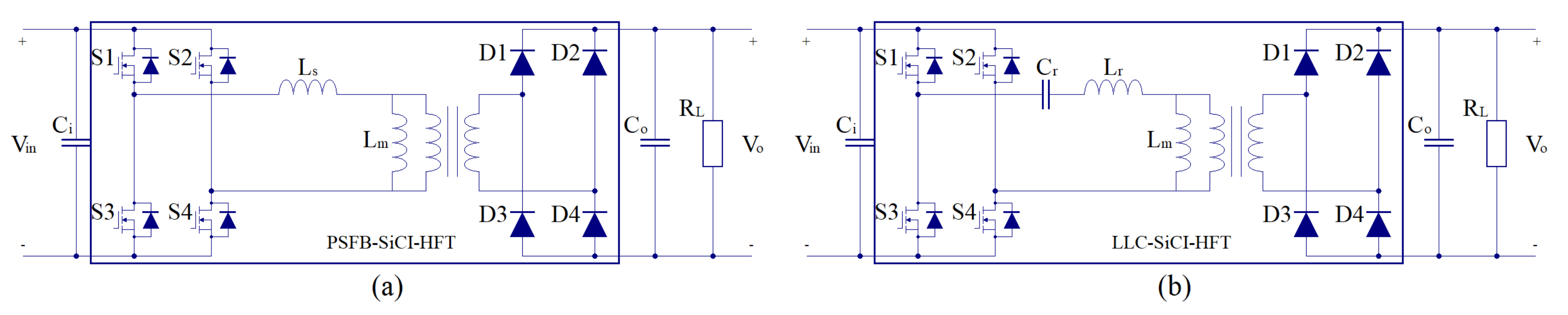
2.2. Phase-Shift Full-Bridge and Full-Bridge LLC DC–DC Converters
- A.
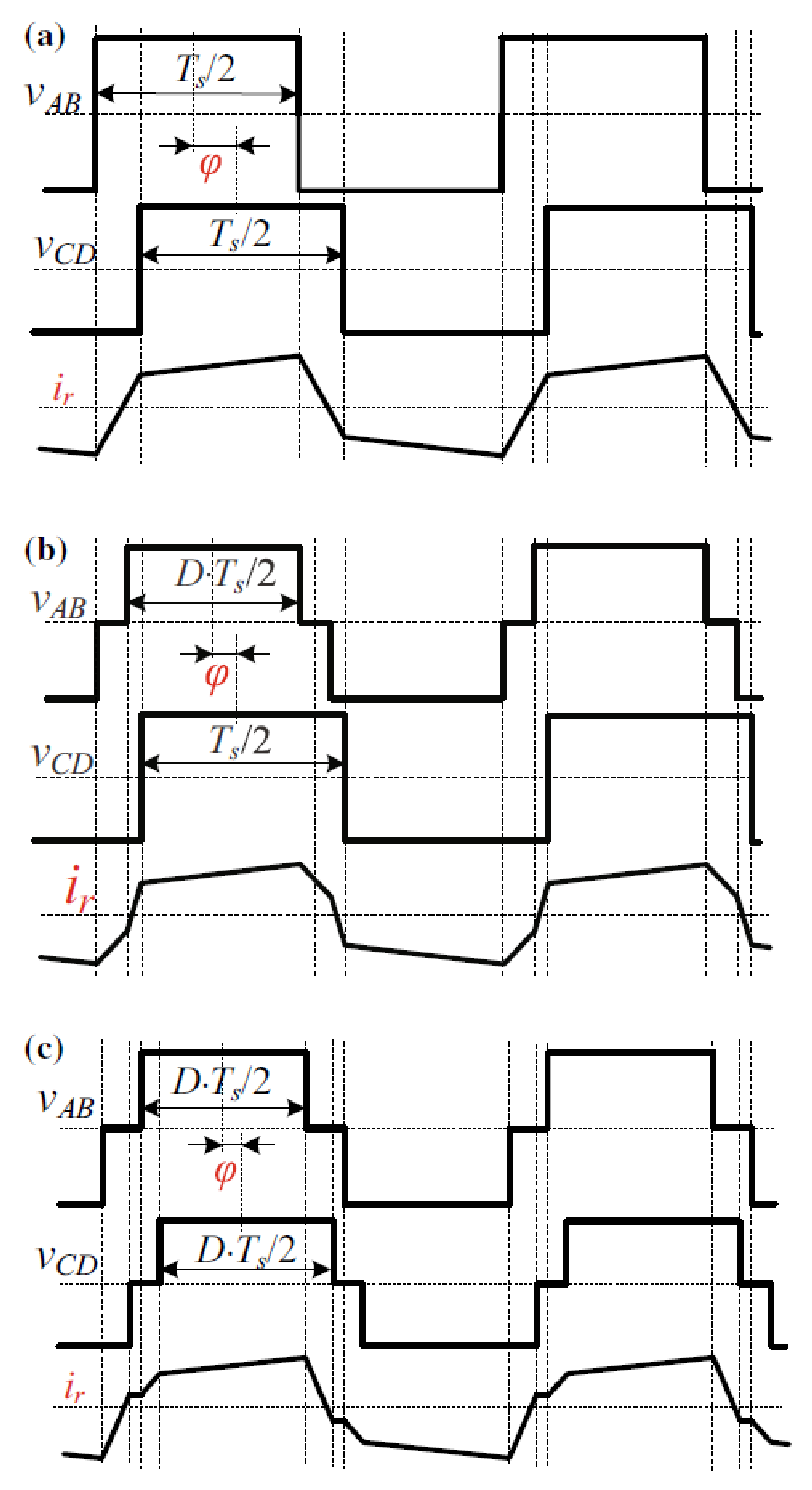
- Phase-Shift Full-Bridge Converters
- B.
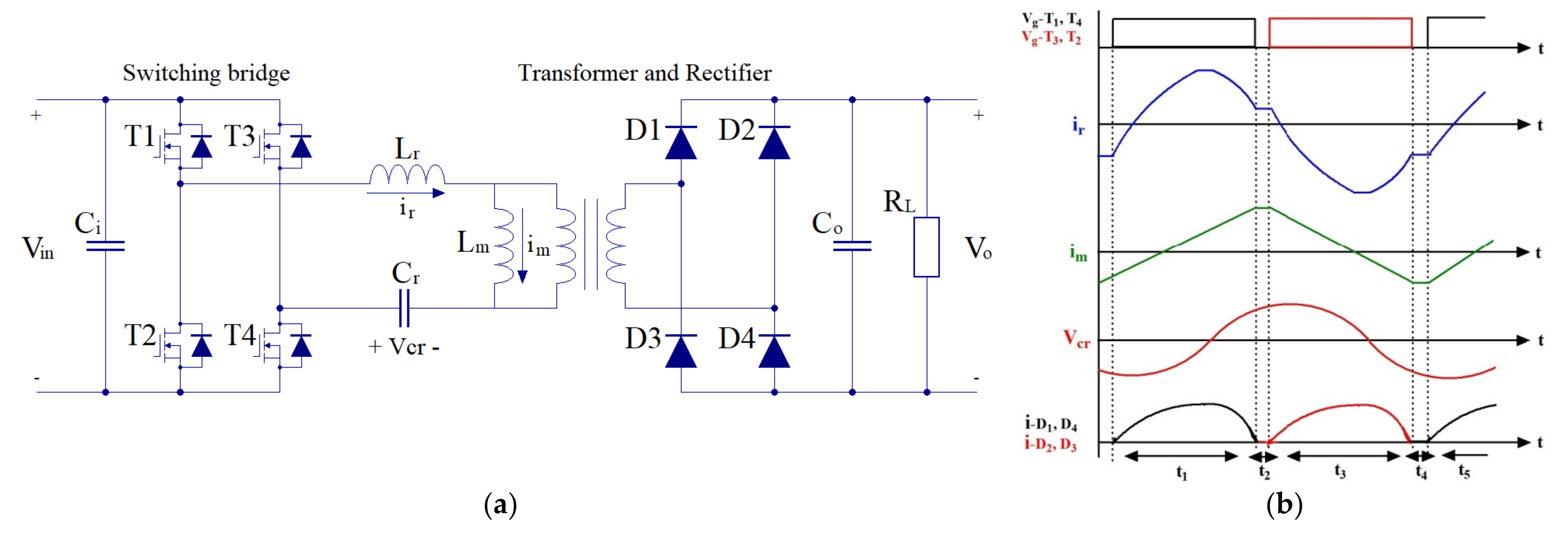
- Full-Bridge LLC Resonant Converters
2.3. Bidirectional Phase-Shift Full-Bridge and Full-Bridge CLLC DC–DC Converters
- A.
- Bidirectional Phase-Shift Full-Bridge Converters
- B.
- Bidirectional Full-Bridge CLLC Resonant Converters
2.4. Comparison between Phase-Shift Full-Bridge/Bidirectional Phase-Shift Full-Bridge Converters and Full-Bridge LLC/Bidirectional Full-Bridge CLLC Resonant Converters
3. Architecture of Integrated SiC-Device and High-Frequency Transformer
3.1. Compact Structure of Integrated SiC-Device and High-Frequency Transformer
3.2. Design Considerations of SiC-Device-Integrated High-Frequency Transformer
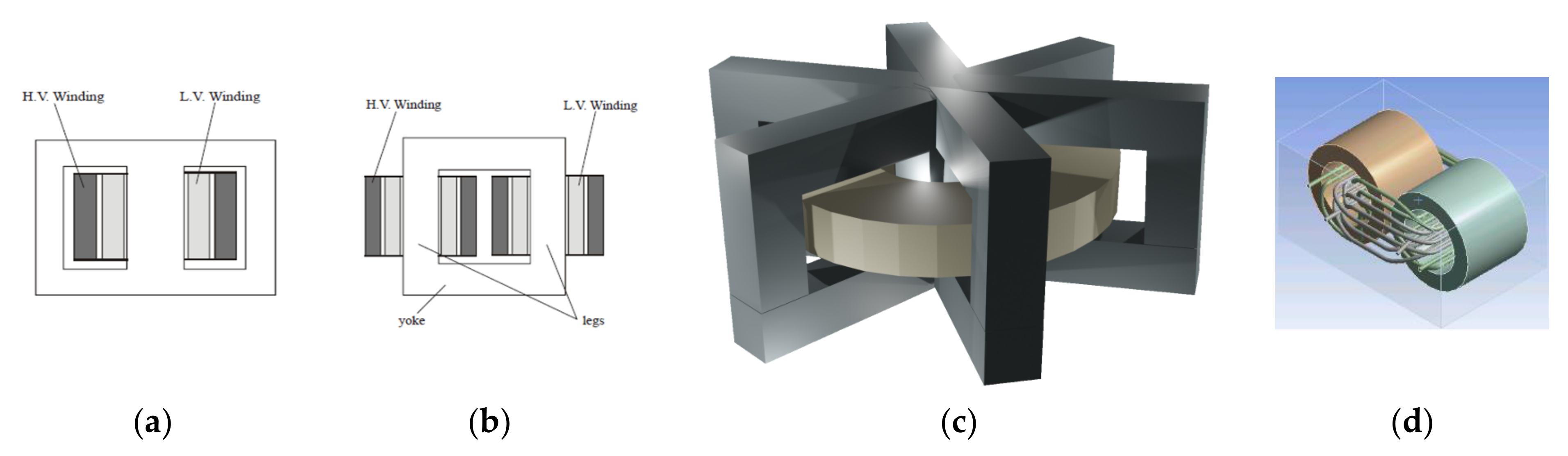
3.2.1. Winding Structures
3.2.2. Electromagnetic Compatibility
3.2.3. Thermal Management and Cooling Methods
4. Design and Implementation of SiC-Device-Integrated High-Frequency Transformer
4.1. Transformer Core Material and SiC Device Selection
4.2. Transformer Design Method for Phase-Shift Full-Bridge and Full-Bridge LLC Converters
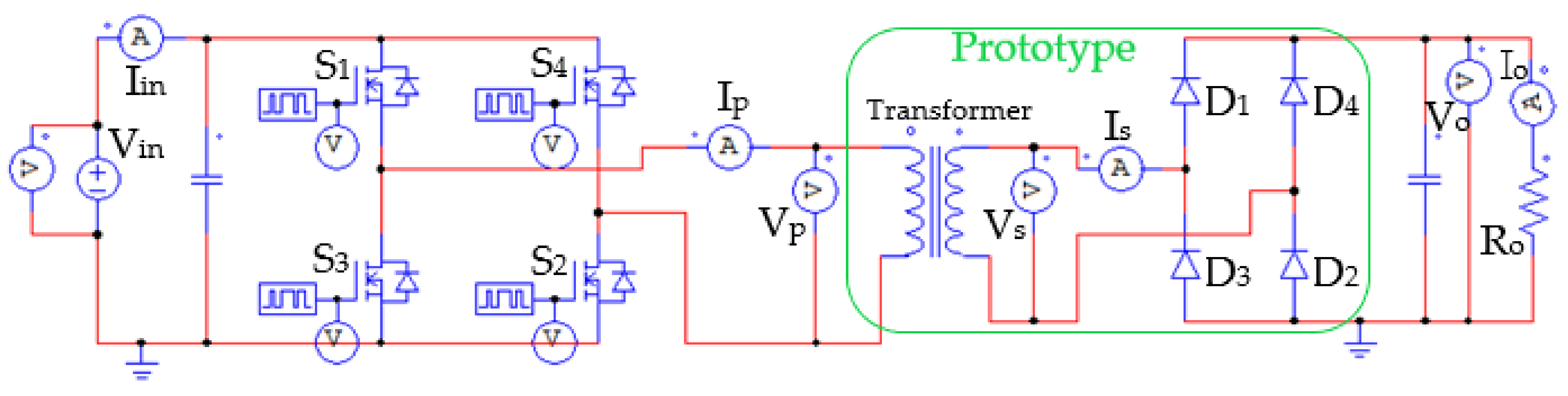
4.3. Simulation and Experimental Results
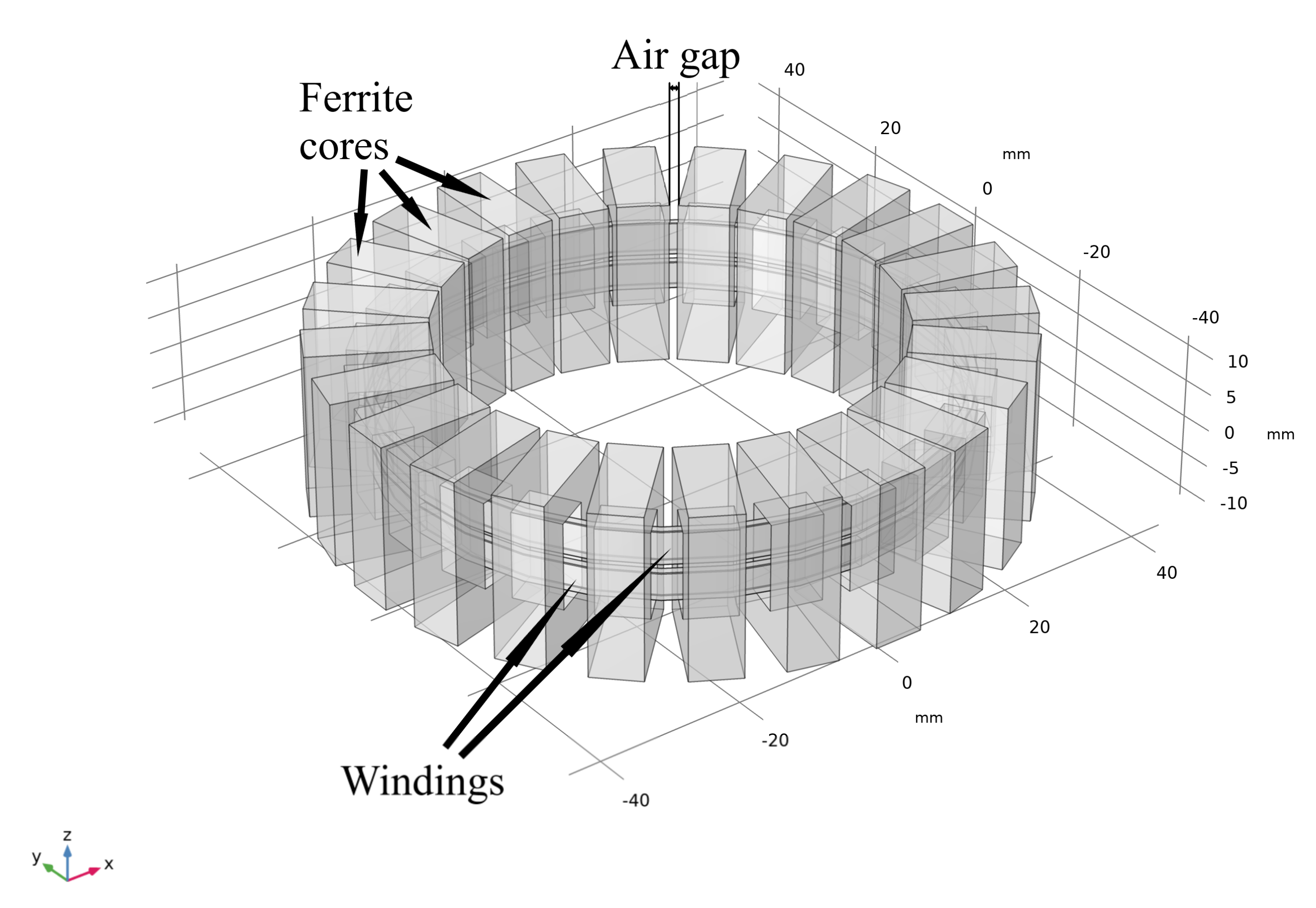
4.3.1. 3D FEM Simulation Results
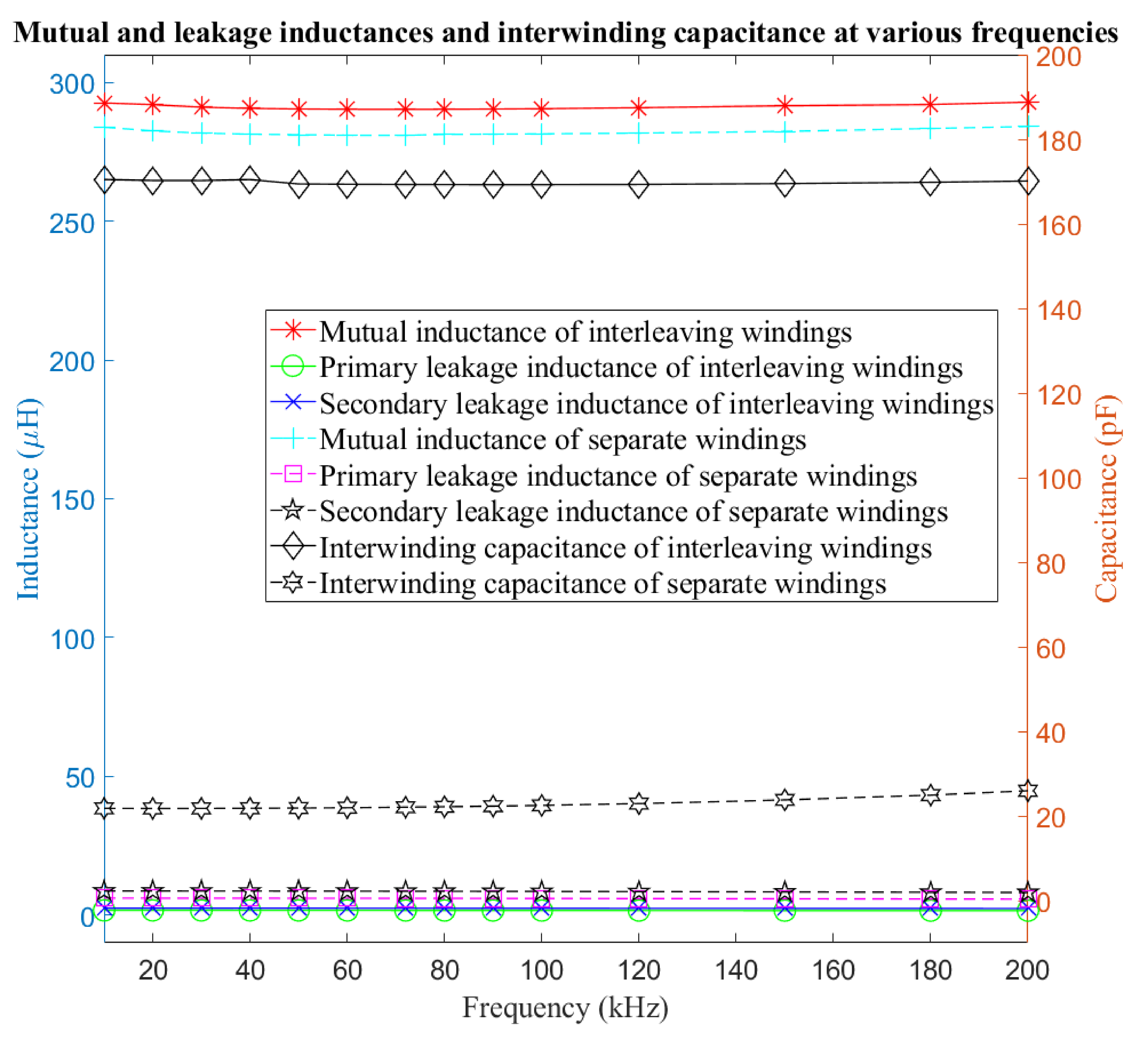
4.3.2. Impedance and Waveform Response Testing Results
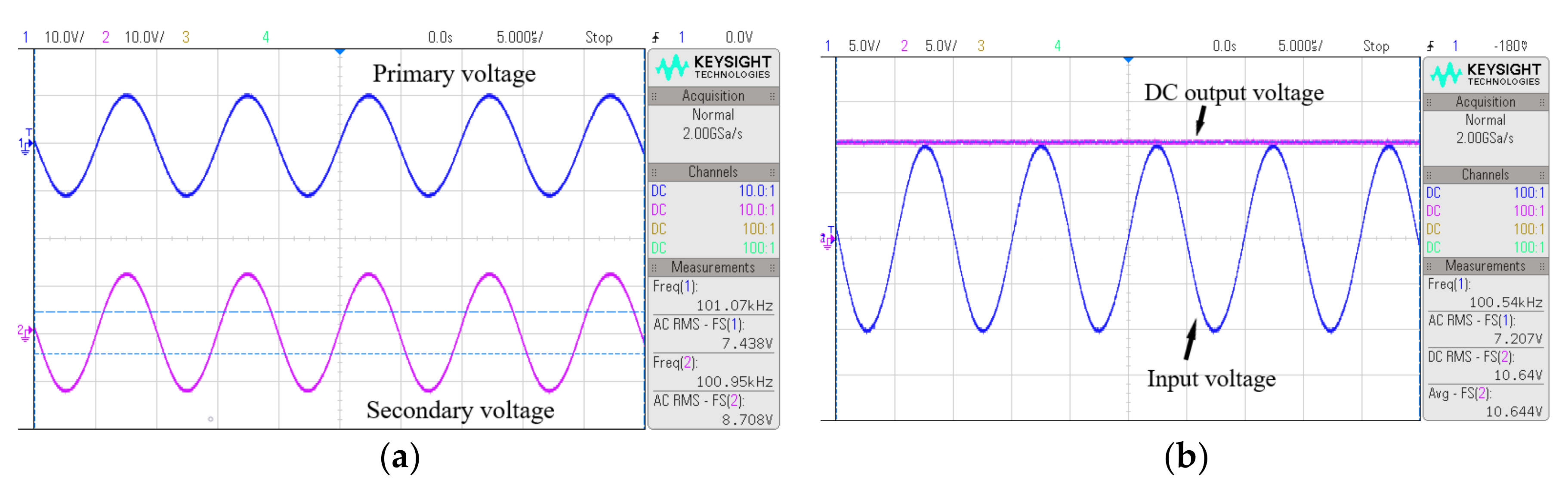
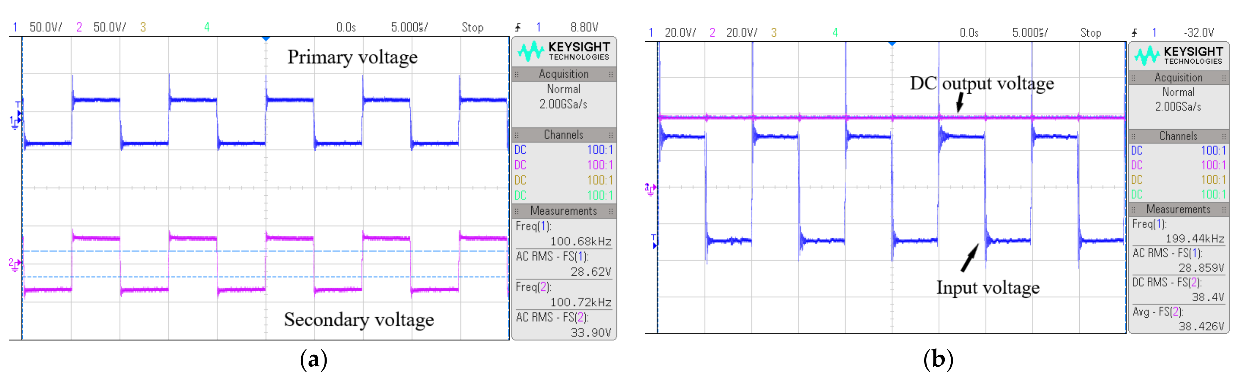
4.3.3. PSIM Power Converter Simulation Results
5. Conclusions
Author Contributions
Funding
Data Availability Statement
Acknowledgments
Conflicts of Interest
References
- Guo, Z.; Sha, D. Introduction. In New Topologies and Modulation Schemes for Soft-Switching Isolated DC–DC Converters; Chen, W., Chen, Y., He, X., Li, Y., Liu, J., Luo, A., Ma, X., Ruan, X., Eds.; CPSS Power Electronics Series; Springer: Singapore, 2020; pp. 1–16. [Google Scholar]
- Baars, N.H.; Everts, J.; Huisman, H.; Duarte, J.L.; Lomonova, E.A. A 80-kW Isolated DC–DC Converter for Railway Applications. IEEE Trans. Power Electron. 2015, 30, 6639–6647. [Google Scholar] [CrossRef]
- Xue, F.; Yu, R.; Huang, A.Q. A 98.3% Efficient GaN Isolated Bidirectional DC–DC Converter for DC Microgrid Energy Storage System Applications. IEEE Trans. Ind. Electron. 2017, 64, 9094–9103. [Google Scholar] [CrossRef]
- Inoue, S.; Akagi, H. A Bidirectional Isolated DC–DC Converter as a Core Circuit of the Next-Generation Medium-Voltage Power Conversion System. IEEE Trans. Power Electron. 2007, 22, 535–542. [Google Scholar] [CrossRef]
- Nabih, A.; Gadelrab, R.; Prakash, P.R.; Li, Q.; Lee, F.C. High Power Density 1 MHz 3 kW 400 V-48 V LLC Converter for Datacenters with improved Core Loss and Termination Loss. In Proceedings of the 2021 IEEE Applied Power Electronics Conference and Exposition (APEC), Phoenix, AZ, USA, 14–17 June 2021; pp. 304–309. [Google Scholar]
- Planar Transformers Family. Available online: https://www.paytongroup.com/planar-transformers (accessed on 5 November 2022).
- Planar Magnetics|Introduction. Available online: https://standexelectronics.com/products/planar-magnetics/ (accessed on 5 November 2022).
- HiMAG PLANAR. Available online: https://www.himag.co.uk/ (accessed on 5 November 2022).
- 600 kW XM3 High Performance Dual Three-Phase Inverter. Available online: https://www.wolfspeed.com/crd600da12e-xm3/ (accessed on 5 November 2022).
- Discrete Silicon Carbide MOSFETs. Available online: https://www.wolfspeed.com/products/power/sic-mosfets/ (accessed on 5 November 2022).
- Silicon Carbide Power Modules. Available online: https://www.wolfspeed.com/products/power/sic-power-modules/ (accessed on 5 November 2022).
- ON Semiconductor Corporation. The Difference Between GaN and SiC Transistors. Power Electron. News 2020, 1–6. [Google Scholar]
- SiC Solutions for DC Fast Charging. Available online: https://www.wolfspeed.com/knowledge-center/article/designing-with-silicon-carbide-sic-in-electric-vehicle-dc-fast-chargers/ (accessed on 30 June 2022).
- 11 kW bi-Directional CLLC DC-DC converter with 1200 V and 1700 V CoolSiC™ MOSFETs. Available online: https://www.infineon.com/dgdl/Infineon-UG-2020-31_REF_DAB11KIZSICSYS-UserManual-v01_01-EN.pdf?fileId=5546d46276fb756a0177060f64a829de (accessed on 11 February 2022).
- PMP21495 6.6 kW, bi-Directional, Dual-Active-Bridge CLLLC Resonant Converter Reference Design. Available online: https://www.ti.com/tool/PMP21495 (accessed on 20 September 2022).
- De Doncker, R.W.; Divan, D.M.; Kheraluwala, M.H. A three-phase soft-switched high-power-density DC/DC converter for high-power applications. IEEE Trans. Ind. Appl. 1991, 27, 63–73. [Google Scholar] [CrossRef]
- Tan, N.M.; Abe, T.; Akagi, H. Experimental discussions on operating frequencies of a bidirectional isolated DC-DC converter for a battery energy storage system. In Proceedings of the 2013 IEEE Energy Conversion Congress and Exposition, Denver, CO, USA, 15–19 September 2013; pp. 2333–2340. [Google Scholar]
- Tan, N.M.; Abe, T.; Akagi, H. Topology and application of bidirectional isolated dc-dc converters. In Proceedings of the 8th International Conference on Power Electronics-ECCE Asia, Jeju, Republic of Korea, 30 May–3 June 2011; pp. 1039–1046. [Google Scholar]
- Akagi, H.; Yamagishi, T.; Tan, N.M.L.; Kinouchi, S.-i.; Miyazaki, Y.; Koyama, M. Power-Loss Breakdown of a 750-V 100-kW 20-kHz Bidirectional Isolated DC–DC Converter Using SiC-MOSFET/SBD Dual Modules. IEEE Trans. Ind. Appl. 2015, 51, 420–428. [Google Scholar] [CrossRef]
- Deng, C.; Xu, D.; Zhang, Y.; Chen, Y.; Okuma, Y.; Mino, K. Impact of dielectric material on passive integration in LLC resonant converter. In Proceedings of the 2008 IEEE Power Electronics Specialists Conference, Rhodes, Greece, 15–19 June 2008; pp. 269–272. [Google Scholar]
- Costa, L.F.; Buticchi, G.; Liserre, M. Highly Efficient and Reliable SiC-Based DC–DC Converter for Smart Transformer. IEEE Trans. Ind. Electron. 2017, 64, 8383–8392. [Google Scholar] [CrossRef]
- Panda, K.P.; Rout, S. A Cost-Effective Design and Analysis of Full Bridge LLC Resonant Converter. World Acad. Sci. Eng. Technol. Int. J. Energy Power Eng. 2016, 10, 1143–1150. [Google Scholar] [CrossRef]
- Beiranvand, R.; Rashidian, B.; Zolghadri, M.R.; Alavi, S.M.H. Using LLC Resonant Converter for Designing Wide-Range Voltage Source. IEEE Trans. Ind. Electron. 2011, 58, 1746–1756. [Google Scholar] [CrossRef]
- Musavi, F.; Craciun, M.; Gautam, D.S.; Eberle, W.; Dunford, W.G. An LLC Resonant DC–DC Converter for Wide Output Voltage Range Battery Charging Applications. IEEE Trans. Power Electron. 2013, 28, 5437–5445. [Google Scholar] [CrossRef]
- Huang, H. Designing an LLC Resonant Half-Bridge Power Converter; Texas Instruments Inc.: Dallas, TX, USA, 2011; pp. 1–27. [Google Scholar]
- Abdel-Rahman, S. Resonant LLC Converter: Operation and Design 250W 33Vin 400Vout Design Example; Application Note AN 2012-09; Infineon Technologies North America (IFNA) Corp.: Durham, NC, USA, 2012; pp. 1–19. [Google Scholar]
- Choi, H. Design Considerations for an LLC Resonant Converter; Fairchild Semiconductor: Sunnyvale, CA, USA, 2007; pp. 82–83. [Google Scholar]
- Gu, Y.; Hang, L.; Chen, H.; Lu, Z.; Qian, Z.; Li, J. A simple structure of LLC resonant DC-DC converter for multi-output applications. In Proceedings of the Twentieth Annual IEEE Applied Power Electronics Conference and Exposition, APEC 2005, Austin, TX, USA, 6–10 March 2005; pp. 1485–1490. [Google Scholar]
- Lu, B.; Liu, W.; Liang, Y.; Lee, F.C.; van Wyk, J.D. Optimal design methodology for LLC resonant converter. In Proceedings of the Twenty-First Annual IEEE Applied Power Electronics Conference and Exposition, APEC’06, Dallas, TX, USA, 19–23 March 2006; pp. 533–538. [Google Scholar]
- Adireddy, R.; Pratap, K.N.G.A.; Himaja, T.; Murthy, K.V.S.R. Circuit analysis and modelling of dual active bridge bidirectional converter. Mater. Today Proc. 2022, 56, 3272–3275. [Google Scholar] [CrossRef]
- Taghizadeh, S.; Hossain, M.J.; Lu, J. Bidirectional isolated vehice to grid (V2G) system: An optimized implementation and approach. In Proceedings of the 2015 IEEE PES Asia-Pacific Power and Energy Engineering Conference (APPEEC), Brisbane, QLD, Australia, 15–18 November 2015; pp. 1–5. [Google Scholar]
- Yade, O.; Gauthier, J.-Y.; Lin-Shi, X.; Gendrin, M.; Zaoui, A. Modulation strategy for a Dual Active Bridge converter using Model Predictive Control. In Proceedings of the 2015 IEEE International Symposium on Predictive Control of Electrical Drives and Power Electronics (PRECEDE), Valparaiso, Chile, 5–6 October 2015; pp. 15–20. [Google Scholar]
- Akagi, H.; Kinouchi, S.-i.; Miyazaki, Y. Bidirectional isolated dual-active-bridge (DAB) DC-DC converters using 1.2-kV 400-A SiC-MOSFET dual modules. CPSS Trans. Power Electron. Appl. 2016, 1, 33–40. [Google Scholar] [CrossRef]
- Alonso, A.R.; Sebastian, J.; Lamar, D.G.; Hernando, M.M.; Vazquez, A. An overall study of a Dual Active Bridge for bidirectional DC/DC conversion. In Proceedings of the 2010 IEEE Energy Conversion Congress and Exposition, Atlanta, GA, USA, 12–16 September 2010; pp. 1129–1135. [Google Scholar]
- Singh, R.; Taghizadeh, S.F.; Tan, N.M.L. Battery energy storage system for PV output leveling based on bidirectional isolated DC-DC converter. In Proceedings of the 2013 IEEE Student Conference on Research and Development, Putrajaya, Malaysia, 16–17 December 2013; pp. 84–89. [Google Scholar]
- Farooq, Z.; Ullah, N. Single-phase shift control for dual active bridge using adaptive PI control technique. Int. J. Power Energy Syst. 2019, 39, 148–155. [Google Scholar] [CrossRef]
- Meena, K.; Jayaswal, K.; Palwalia, D.K. Analysis of Dual Active Bridge Converter for Solid State Transformer Application using Single-Phase Shift Control Technique. In Proceedings of the 2020 International Conference on Inventive Computation Technologies (ICICT), Coimbatore, India, 26–28 February 2020; pp. 1–6. [Google Scholar]
- Zhao, B.; Yu, Q.; Sun, W. Extended-Phase-Shift Control of Isolated Bidirectional DC–DC Converter for Power Distribution in Microgrid. IEEE Trans. Power Electron. 2012, 27, 4667–4680. [Google Scholar] [CrossRef]
- Shi, H.; Wen, H.; Chen, J.; Hu, Y.; Jiang, L.; Chen, G.; Ma, J. Minimum-Backflow-Power Scheme of DAB-Based Solid-State Transformer with Extended-Phase-Shift Control. IEEE Trans. Ind. Appl. 2018, 54, 3483–3496. [Google Scholar] [CrossRef]
- Oggier, G.G.; García, G.O.; Oliva, A.R. Switching Control Strategy to Minimize Dual Active Bridge Converter Losses. IEEE Trans. Power Electron. 2009, 24, 1826–1838. [Google Scholar] [CrossRef]
- Oggier, G.G.; García, G.O.; Oliva, A.R. Modulation strategy to operate the dual active bridge DC-DC converter under soft switching in the whole operating range. IEEE Trans. Power Electron. 2011, 26, 1228–1236. [Google Scholar] [CrossRef]
- Zhao, B.; Song, Q.; Liu, W. Efficiency Characterization and Optimization of Isolated Bidirectional DC–DC Converter Based on Dual-Phase-Shift Control for DC Distribution Application. IEEE Trans. Power Electron. 2013, 28, 1711–1727. [Google Scholar] [CrossRef]
- Zhao, B.; Song, Q.; Liu, W.; Sun, W. Current-Stress-Optimized Switching Strategy of Isolated Bidirectional DC–DC Converter with Dual-Phase-Shift Control. IEEE Trans. Ind. Electron. 2013, 60, 4458–4467. [Google Scholar] [CrossRef]
- Feng, B.; Wang, Y.; Man, J. A novel dual-phase-shift control strategy for dual-active-bridge DC-DC converter. In Proceedings of the IECON 2014—40th Annual Conference of the IEEE Industrial Electronics Society, Dallas, TX, USA, 29 October–1 November 2014; pp. 4140–4145. [Google Scholar]
- Bai, H.; Mi, C. Eliminate Reactive Power and Increase System Efficiency of Isolated Bidirectional Dual-Active-Bridge DC–DC Converters Using Novel Dual-Phase-Shift Control. IEEE Trans. Power Electron. 2008, 23, 2905–2914. [Google Scholar] [CrossRef]
- Calderon, C.; Barrado, A.; Rodriguez, A.; Alou, P.; Lazaro, A.; Fernandez, C.; Zumel, P. General Analysis of Switching Modes in a Dual Active Bridge with Triple Phase Shift Modulation. Energies 2018, 11, 2419. [Google Scholar] [CrossRef] [Green Version]
- Wen, H.; Xiao, W. Bidirectional dual-active-bridge DC-DC converter with triple-phase-shift control. In Proceedings of the 2013 Twenty-Eighth Annual IEEE Applied Power Electronics Conference and Exposition (APEC), Long Beach, CA, USA, 17–21 March 2013; pp. 1972–1978. [Google Scholar]
- Harrye, Y.A.; Ahmed, K.H.; Adam, G.P.; Aboushady, A.A. Comprehensive steady state analysis of bidirectional dual active bridge DC/DC converter using triple phase shift control. In Proceedings of the 2014 IEEE 23rd International Symposium on Industrial Electronics (ISIE), Istanbul, Turkey, 1–4 June 2014; pp. 437–442. [Google Scholar]
- Huang, J.; Wang, Y.; Gao, Y.; Lei, W.; Li, Y. Unified PWM control to minimize conduction losses under ZVS in the whole operating range of dual active bridge converters. In Proceedings of the 2013 Twenty-Eighth Annual IEEE Applied Power Electronics Conference and Exposition (APEC), Long Beach, CA, USA, 17–21 March 2013; pp. 2016–2022. [Google Scholar]
- Kumar, A.; Bhat, A.H.; Agarwal, P. Comparative analysis of dual active bridge isolated DC to DC converter with double phase shift and triple phase shift control techniques. In Proceedings of the 2017 Recent Developments in Control, Automation & Power Engineering (RDCAPE), Noida, India, 26–27 October 2017; pp. 257–262. [Google Scholar]
- Jung, J.-H.; Kim, H.-S.; Ryu, M.-H.; Baek, J.-W. Design Methodology of Bidirectional CLLC Resonant Converter for High-Frequency Isolation of DC Distribution Systems. IEEE Trans. Power Electron. 2013, 28, 1741–1755. [Google Scholar] [CrossRef]
- Rezayati, M.; Tahami, F.; Schanen, J.-L.; Sarrazin, B. Generalized State-Plane Analysis of Bidirectional CLLC Resonant Converter. IEEE Trans. Power Electron. 2022, 37, 5773–5785. [Google Scholar] [CrossRef]
- Zhao, B.; Zhang, X.; Hunag, J. Design of CLLC Resonant Converters for the Hybrid AC/DC Microgrid Applications. In Proceedings of the 2018 IEEE International Power Electronics and Application Conference and Exposition (PEAC), Shenzhen, China, 4–7 November 2018; pp. 1–5. [Google Scholar]
- Zahid, Z.U.; Dalala, Z.M.; Chen, R.; Chen, B.; Lai, J.-S. Design of Bidirectional DC–DC Resonant Converter for Vehicle-to-Grid (V2G) Applications. IEEE Trans. Transp. Electrif. 2015, 1, 232–244. [Google Scholar] [CrossRef]
- Hunag, J.; Zhang, X.; Shuai, Z.; Zhang, X.; Wang, P.; Koh, L.H.; Xiao, J.; Tong, X. Robust Circuit Parameters Design for the CLLC-Type DC Transformer in the Hybrid AC–DC Microgrid. IEEE Trans. Ind. Electron. 2019, 66, 1906–1918. [Google Scholar] [CrossRef]
- Zou, S.; Lu, J.; Mallik, A.; Khaligh, A. Bi-Directional CLLC Converter with Synchronous Rectification for Plug-In Electric Vehicles. IEEE Trans. Ind. Appl. 2018, 54, 998–1005. [Google Scholar] [CrossRef]
- Liu, G.; Li, D.; Zhang, J.Q.; Hu, B.; Jia, M.L. Bidirectional CLLC resonant DC-DC converter with integrated magnetic for OBCM application. In Proceedings of the 2015 IEEE International Conference on Industrial Technology (ICIT), Seville, Spain, 17–19 March 2015; pp. 946–951. [Google Scholar]
- Bahmani, M.A.; Thiringer, T.; Rabiei, A.; Abdulahovic, T. Comparative Study of a Multi-MW High-Power Density DC Transformer with an Optimized High-Frequency Magnetics in All-DC Offshore Wind Farm. IEEE Trans. Power Deliv. 2016, 31, 857–866. [Google Scholar] [CrossRef]
- Bahmani, M.A.; Agheb, E.; Thiringer, T.; Høidalen, H.K.; Serdyuk, Y. Core loss behavior in high frequency high power transformers—I: Effect of core topology. J. Renew. Sustain. Energy 2012, 4, 033112. [Google Scholar] [CrossRef]
- Shamshuddin, M.A.; Rojas, F.; Cardenas, R.; Pereda, J.; Diaz, M.; Kennel, R. Solid State Transformers: Concepts, Classification, and Control. Energies 2020, 13, 2319. [Google Scholar] [CrossRef]
- Ortiz, G.; Biela, J.; Bortis, D.; Kolar, J.W. 1 Megawatt, 20 kHz, Isolated, bidirectional 12 kV to 1.2 kV DC-DC converter for renewable energy applications. In Proceedings of the International Power Electronics Conference, Sapporo, Japan, 21–24 June 2010; pp. 3212–3219. [Google Scholar]
- Villar, I.; Garcia-Bediaga, A.; Viscarret, U.; Etxeberria-Otadui, I.; Rufer, A. Proposal and validation of medium-frequency power transformer design methodology. In Proceedings of the 2011 IEEE Energy Conversion Congress and Exposition, Phoenix, AZ, USA, 17–22 September 2011; pp. 3792–3799. [Google Scholar]
- Water, W.; Lu, J. Shielding Analysis of High-Frequency Coaxial Transformers Used for Electric Vehicle On-Board Charging Systems. IEEE Trans. Magn. 2013, 49, 4005–4008. [Google Scholar] [CrossRef]
- Lu, J.; Dawson, F. Characterizations of High Frequency Planar Transformer with a Novel Comb-Shaped Shield. IEEE Trans. Magn. 2011, 47, 4493–4496. [Google Scholar] [CrossRef]
- Water, W.; Lu, J. Improved High-Frequency Planar Transformer for Line Level Control (LLC) Resonant Converters. IEEE Magn. Lett. 2013, 4, 6500204. [Google Scholar] [CrossRef]
- Erickson, R.W.; Maksimović, D. Fundamentals of Power Electronics, 3rd ed.; Springer: Cham, Switzerland, 2020; pp. 426–443. [Google Scholar]
- McLyman, C.W.T. Transformer and Inductor Design Handbook, 4th ed.; CRC Press: Boca Raton, FL, USA, 2011; pp. 4-1–4-42. [Google Scholar]
- Yao, W.; Parveen, T.; Lu, J.; Seagar, A. Modular High-Frequency High-Power Transformers for Offshore Wind Turbines. In Proceedings of the 2021 IEEE PES Innovative Smart Grid Technologies—Asia (ISGT Asia), Brisbane, Australia, 5–8 December 2021; pp. 1–5. [Google Scholar]
- Barrios, E.L.; Urtasun, A.; Ursúa, A.; Marroyo, L.; Sanchis, P. High-Frequency Power Transformers with Foil Windings: Maximum Interleaving and Optimal Design. IEEE Trans. Power Electron. 2015, 30, 5712–5723. [Google Scholar] [CrossRef]
- Zhao, B.; Ouyang, Z.; Duffy, M.C.; Andersen, M.A.E.; Hurley, W.G. An Improved Partially Interleaved Transformer Structure for High-Voltage High-Frequency Multiple-Output Applications. IEEE Trans. Ind. Electron. 2019, 66, 2691–2702. [Google Scholar] [CrossRef]
- Bowen, D.; Lee, A.; Krafft, C.; Mayergoyz, I.D. Design Control of Performance in Nested and Interleaved Winding Printed Circuit Board Transformers for Ethernet Applications. IEEE Trans. Magn. 2013, 49, 4013–4016. [Google Scholar] [CrossRef]
- Chen, B. Analysis of Effect of Winding Interleaving on Leakage Inductance and Winding Loss of High Frequency Transformers. J. Electr. Eng. Technol. 2019, 14, 1211–1221. [Google Scholar] [CrossRef]
- Venugopal, A.; Robert, F. Analysis of a Non-overlapping Interleaved Planar Transformer Winding Structure with Reduced Parasitic Effects. Iran. J. Sci. Technol. Trans. Electr. Eng. 2022, 46, 689–700. [Google Scholar] [CrossRef]
- Petrescu, M.C.; Petrescu, L.; Cazacu, E. Influence of Planar Transformer Windings Interleaving on Parasitic Parameters. Electroteh. Electron. Autom. 2018, 66, 45–50. [Google Scholar]
- Shimura, K.; Tanaka, M.; Satou, M.; Mizuno, T. Copper Loss Reduction in Planar Transformer for LLC Resonant Converter Using Interleaved Winding. J. Jpn. Soc. Appl. Electromagn. Mech. 2020, 28, 128–133. [Google Scholar] [CrossRef]
- Otsu, S.; Nakamura, K. Characteristics of DC-DC Converter using High-Frequency Amorphous Transformer with Interleaved-Winding for HVDC Transmission System. Trans. Magn. Soc. Jpn. Spec. Issues 2020, 4, 81–85. [Google Scholar] [CrossRef]
- Zhu, B. The Electromagnetic Compatibility Problems of Integrated Circuits. Ph.D. Thesis, Griffith University, Brisbane, Australia, 2011. [Google Scholar]
- Wu, Y.; Yin, S.; Liu, Z.; Li, H.; See, K.Y. Experimental Investigation on Electromagnetic Interference (EMI) in Motor Drive Using Silicon Carbide (SiC) MOSFET. In Proceedings of the 2020 International Symposium on Electromagnetic Compatibility-EMC EUROPE, Rome, Italy, 23–25 September 2020; pp. 1–6. [Google Scholar]
- Wu, Y.; Zhang, H.; Yin, S.; Lin, S.; Jiang, T.; Bi, C.; Li, H.; Cheng, Y. Investigation of Conducted Electromagnetic Interference of Three-Level SiC Power Module. In Proceedings of the 2022 Asia-Pacific International Symposium on Electromagnetic Compatibility (APEMC), Beijing, China, 1–4 September 2022; pp. 698–701. [Google Scholar]
- Ma, W.; Wu, Y.; Li, H.; Chu, D. Investigation of the Gate Resistance and the RC snubbers on the EMI Suppression in Applying of the SiC MOSFET. In Proceedings of the 2019 IEEE International Conference on Mechatronics and Automation (ICMA), Tianjin, China, 4–7 August 2019; pp. 2224–2228. [Google Scholar]
- Zheng, L.; Han, X.; An, Z.; Kandula, R.P.; Kandasamy, K.; Saeedifard, M.; Divan, D. SiC-Based 5-kV Universal Modular Soft-Switching Solid-State Transformer (M-S4T) for Medium-Voltage DC Microgrids and Distribution Grids. IEEE Trans. Power Electron. 2021, 36, 11326–11343. [Google Scholar] [CrossRef]


| Power Electronic Topology | Unidirectional FB-LLC | Unidirectional PSFB | Bidirectional FB-CLLC | Bidirectional PSFB |
|---|---|---|---|---|
| Suitability of I-SiC-HFT | High | High | High | High |
| Magnetic component design | Easy | Easy | Easy | Easy |
| Switching loss | Low | Medium | Low | Medium |
| EMI problem | Low | Low | Low | Low |
| Power loss | Low | Low | Low | Low |
| Thermal problem | Less | Less | Less | Less |
| Power efficiency | >98% | >98% | >98% | >98% |
| High-power applications | Yes | Yes | Yes | Yes |
| Transformer Type/Structure | Advantages | Disadvantages |
|---|---|---|
| Core type | Easy to repair Well-suited for HP applications | Poor cooling Less mechanical protection to coils Difficult to tune leakage inductance |
| Shell type | Effective cooling Better mechanical protection to coils Well-suited for HP applications | Not easy to repair |
| Pot core transformer | Better mechanical protection to coils Low EMI problem High power density | Low power ratings |
| Toroidal transformer | Easy to construct and repair | Less mechanical protection to coils High EMI problem |
| Coaxial transformer | Suitable for HF applications | Low power ratings |
| Planar transformer | Small in size and weight Low to medium power applications | High interwinding capacitance |
| Matrix transformer | Advantages of both core and shell-type transformers | Higher weight and volume Difficult to tune leakage inductance |
| Proposed transformer | Advantages of both core-type, shell-type, and pot core transformers Integration with SiC devices feasible | Not well-suited for very low-power applications—higher weight and volume |
| Variable | Value |
|---|---|
| Power rating | 1.5 kW |
| Rated primary voltage | 375 Vrms |
| Rated primary current | 4 A |
| Operating frequency | 100 kHz |
| Maximum current density | 5 × 10⁶ A/m2 (5 A/mm2) |
| Window utilization factor | ≤0.25 |
| Type of transformer | Isolation transformer |
| Electromagnetic Property of N27 | Value |
|---|---|
| Resistivity | 3 Ω·m |
| Initial relative permeability | 2000 |
| Saturation flux density | 0.41 T 1 |
| Core loss density | 920 kW/m3 2 |
| Operating frequency range | up to 150 kHz |
| Characteristics of S3D06065 | Condition | Value |
|---|---|---|
| DC blocking voltage, Peak repetitive reverse voltage, Working peak reverse voltage | - | 650 V |
| Average rectified forward current | Tc = 157 °C | 6 A |
| Forward voltage drop | 6A, pulse, TJ = 175 °C | 1.9–2.4 V |
| Junction capacitance | VR = 0 V, TJ = 25 °C, f = 1 MHz | 382 pF |
| Power dissipation | TJ = 110 °C | 45 W |
| Transformer Parameter | Designed Value |
|---|---|
| Number of pairs of U cores | 24 |
| Maximum magnetic flux density | 0.3 T |
| Number of strands for primary coil | 7 strands |
| Number of strands for secondary coil | 7 strands |
| Number of primary turns | 5 turns |
| Number of secondary turns | 6 turns |
| Turns ratio | 1:1.2 |
| Transformer Parameter | Simulated Value |
|---|---|
| Maximum magnetic flux density | 0.33604 T |
| Mutual inductance | 281.51 μH |
| Primary leakage inductance | 5.7404 μH |
| Secondary leakage inductance | 8.2660 μH |
| Voltage ratio | 1.1955 |
| Primary voltage | 375.53 V |
| Secondary voltage | 448.95 V |
| Primary current | 3.9943 A |
| Secondary current | 3.3255 A |
| Primary power | 1499.979 W |
| Secondary power | 1492.983 W |
| Transformer efficiency | 99.53% |
| Maximum Flux Density in Ferrite Cores | Maximum Leakage Flux Density in Windings | Maximum Leakage Flux Density in Air |
|---|---|---|
| 0.33604 T | 6.42 mT | 5.48 mT |
| Winding | Test Item | Primary | Secondary | |
|---|---|---|---|---|
| Separate | Open-circuit test | Rp (kΩ) | 159.71 | 173.77 |
| Lp (μH) | 235.41 | 339.08 | ||
| Short-circuit test | Rs (mΩ) | 301.81 | 439.10 | |
| Ls (μH) | 5.9862 | 8.4830 | ||
| Interwinding capacitance | 22.488 pF | |||
| Turns ratio | 1.20 | |||
| Phase difference | +0.1144° | |||
| Mutual inductance | 281.47 μH | |||
| Coupling coefficient | 0.996 | |||
| Interleaved | Open-circuit test | Rp (kΩ) | 142.90 | 155.56 |
| Lp (μH) | 242.48 | 349.46 | ||
| Short-circuit test | Rs (mΩ) | 125.94 | 173.03 | |
| Ls (μH) | 1.6567 | 2.4290 | ||
| Interwinding capacitance | 169.28 pF | |||
| Turns ratio | 1.20 | |||
| Phase difference | +0.0788° | |||
| Mutual inductance | 290.54 μH | |||
| Coupling coefficient | 0.998 | |||
| Circuit Inductance | Simulated | Measured | Difference |
|---|---|---|---|
| Mutual | 281.51 μH | 281.47 μH | 0.02% |
| Primary leakage | 5.7404 μH | 5.9862 μH | 4.2% |
| Secondary leakage | 8.2660 μH | 8.4830 μH | 2.6% |
| Parameter | DC Source | Transformer Primary Side | Transformer Secondary Side | DC Output | Transformer Efficiency | Prototype I-SiC-HFT Efficiency | Overall Efficiency |
|---|---|---|---|---|---|---|---|
| Voltage | 375 V | 370.9 V | 439.1 V | 432.47 V | 99.57% | 93.62% | 90.11% |
| Current | 4.10 A | 3.99 A | 3.356 A | 3.2035 A | |||
| Power | 1537.5 W | 1479.891 W | 1473.6196 W | 1385.4176 W |
Disclaimer/Publisher’s Note: The statements, opinions and data contained in all publications are solely those of the individual author(s) and contributor(s) and not of MDPI and/or the editor(s). MDPI and/or the editor(s) disclaim responsibility for any injury to people or property resulting from any ideas, methods, instructions or products referred to in the content. |
© 2023 by the authors. Licensee MDPI, Basel, Switzerland. This article is an open access article distributed under the terms and conditions of the Creative Commons Attribution (CC BY) license (https://creativecommons.org/licenses/by/4.0/).
Share and Cite
Yao, W.; Lu, J.; Taghizadeh, F.; Bai, F.; Seagar, A. Integration of SiC Devices and High-Frequency Transformer for High-Power Renewable Energy Applications. Energies 2023, 16, 1538. https://doi.org/10.3390/en16031538
Yao W, Lu J, Taghizadeh F, Bai F, Seagar A. Integration of SiC Devices and High-Frequency Transformer for High-Power Renewable Energy Applications. Energies. 2023; 16(3):1538. https://doi.org/10.3390/en16031538
Chicago/Turabian StyleYao, Weichong, Junwei Lu, Foad Taghizadeh, Feifei Bai, and Andrew Seagar. 2023. "Integration of SiC Devices and High-Frequency Transformer for High-Power Renewable Energy Applications" Energies 16, no. 3: 1538. https://doi.org/10.3390/en16031538