Article

A Design and Validation of 400 W PV Emulator Using Simple Equivalent Circuit for PV Power System Test

College of IT Convergence Engineering, Gachon University, Seongnam 13120, Republic of Korea
*
Author to whom correspondence should be addressed.
Energies 2023, 16(4), 1561; https://doi.org/10.3390/en16041561
Submission received: 10 January 2023 / Revised: 25 January 2023 / Accepted: 30 January 2023 / Published: 4 February 2023
(This article belongs to the Section A2: Solar Energy and Photovoltaic Systems)

Abstract

:
In this paper, we propose a photovoltaic emulator (PVE) composed of a series of connected power diodes with a single constant current source, rather than a power converter-based PVE. Accordingly, this enables readily verifying the operation because a the simple hardware structure and lack of a complex control algorithm. The proposed PVE can be intuitively implemented using the proposed selection criteria for the power diode and equivalent resistances. Since there is no feedback control based on complex analog/digital controls and sensors, the control response can be very fast. In addition, the proposed PVE can be easily integrated with a PV power system such as a power optimizer, to allow testing in a simple and flexible manner. Spice simulation was performed based on the electrical characteristics provided by the solar panel manufacturer, and this was utilized to validate the applied emulator circuit model, the Norton Equivalent Circuit. During the design process, the simulation helped to manufacture the PVE within error ranges satisfying the desired I–V and P–V curves, as well as the maximum power point (MPP). Partial shading could be easily implemented through use of the multiple series connection of individual PVEs, demonstrating local MPP and global MPP. A 400 W class PVE was built through appropriate power diode selection, with a thermal design to increase the output power. Moreover, its performance and feasibility were verified through intensive experiments. The measured efficiency, transient response time, and maximum transient error of the partial shading tests were 91%, 22 μs, and 5.8%, respectively.

1. Introduction

The increasing interest in renewable energy sources (solar, wind, fuel cells, hydropower, biomass, geotherm, etc.) has been driven by climate change and the growing environmental concern worldwide. Photovoltaic (PV) energy has many advantages, such as a high efficiency through improved circuit elements, pollution-free generation, low maintenance and operational costs, and economic efficiency from low production costs. Along with government incentives and enhanced technologies for power electronics and battery storage, the demand for PV energy is continuously increasing [1,2,3,4,5].
Constructing an experimental environment using actual PV panels is difficult, because solar power generation is highly dependent on the external environment. ‘Photovoltaic emulators (PVE)’ can be studied for the purpose of emulating the operational characteristics of an actual PV system under various external conditions [6,7]. Under the desired conditions, the PVE can conduct tests using repetitive and consistent methods. In addition, a PVE can implement an I–V curve applying changes of daylight and load. In addition, it can be easily integrated with a power converter/inverter, validating the proper operation of maximum power point tracking (MPPT).
Before the appearance of PVEs, artificial lighting (halogen lamps) and temperature control devices were used to test PVs, but these were problematic due to the significant scale of the required experimental setup, high costs, low convenience, and high-power consumption from the lamps [8,9]. The lookup table (LUT) method was also used, which operates by storing the output characteristics of an actual solar panel as data and using this data as input for a PVE [1]. However, a significant amount of data are required for accurate operation, and the control speed is slow.
Recent research has categorized PVEs into two types: the diode-type PVE, which mainly constitutes series-parallel connected diodes that simulate the operation of a PV cell diode; and the converter-type PVE, which amplifies a reference signal of current–voltage (involving the information of a PV panel) from an equivalent circuit into a higher output signal.
The converter-type PVE is based on a switching mode electric circuit that uses a DC/DC converter. LLC resonant [10], two-stage boost-buck cascaded [11], buck [12], three-phase dc–dc interleaved buck [13], two-switch buck-boost [14], and buck-boost [15] DC/DC converters have been proposed. In recent studies [16,17,18], a variety of nonlinear controllers have been introduced to improve the accuracy of the nonlinear characteristics of the I–V curve as a direct referencing method. In a SEPIC converter [16], a backstepping controller is utilized to adjust according to the desired working points. In a buck converter, a LUT-based gain scheduling [17] and Lyapunov controller [18] are utilized to simulate constantly changing operation points and overcome accuracy problem, respectively. A fractional order sliding mode controller [19] is used in the two-diode model, to achieve robust operations during load changes and disturbances; however, the system parameters should be precisely determined in advanced. On the other hand, a switched-capacitor architecture based PVE [20] was introduced, to consider the reconfigurable and scalable features when simulating mismatched conditions.
While their advantages include a high output voltage, galvanic isolation, ripple minimization, and high efficiency, the limitations include a complex structure, difficult control, high production costs, and slow computing speed. This applies to the electrical properties of a solar panel as signals, which are amplified to the power level by converters. Here, a controller is also necessary to maintain the desired shape (electrical properties of the solar panel). During switching operation and for feedback control, the dynamic response is not fast enough.
In comparison, the composition of the diode-type PVE is simple, its response speed is fast because there are no complex control circuits, and it is accurate because the characteristics of the diode are fully reflected [21,22,23,24]. However, it suffers from high power losses, low efficiency, cumbersome size, and the necessity of a heat sink when the capacity increases. In a review of the existing literature, prototypes were designed for at most 10 W of output power. This is a significantly low capacity for an actual PVE; hence, a practical power capacity for a diode-based PVE needs to be designed.
Since the diode is the core component in the PVE hardware, this factor is the most important for research. Recent literature reports [21,22,23] lacked information on the specifics and selection criteria of the diode. Only the article in [24] presented the specifications of the components that they used. In their study, 27 diodes were connected in series to compose an equivalent circuit, and the standard recovery characteristics of a 1N5400 (reverse voltage: Vr = 50 V, forward voltage: Vf = 1 V, forward current: If = 3 A) diode were applied in the actual hardware. Considering the current margin, the PVE hardware was designed to have an open circuit voltage (VOC) and a short circuit current (ISC) of 21.5 V and 0.65 A, respectively. For this reason, the maximum power was 10 W, which does not comply with actual testing with an MPPT converter. Further research [25] increased this capacity to 80 W. A fast recovery power rectifier, which is a power diode that has a relatively high current, was used; a total of 28 MR860 components were connected in series. A relatively high current diode was used, and due to the requirements of the thermal design, VOC = 21.7 V and ISC = 3.31 A were applied. However, their research also lacked details of the power-increasing design and diode selection criteria.
The main improvements and contributions of this paper include (1) Presenting design guidelines for the power diode, series, and parallel resistances in the diode equivalent circuit model; previous works used signal diodes [1,24,25] without design guidelines and complicated equations for the parameters [26,27]. (2) Extremely fast transient response, without a complicated controller; previous works had a poor dynamic response, even slower than an actual PV panel, because of the controller bandwidth used [10,11]. (3) Designing a high-efficiency diode-type 400 W PVE, which reflects contemporary trends of PV panels; previous works designed prototypes below 100 W using signal diodes [1,24,25]. (4) Scalability of the prototype for partial shading tests using multiple series connections; previous works had difficulty in achieving series connections. (5) Reconfigurable prototype to modify the PV curve; previous works changed the analog circuit [13], reference signal [10,11,12,13,14,15], or LUT [17].
The rest of the paper is structured as follows: In Section 2, PV cell characteristics are described, to highlight the recent tendencies in PV panels, and the validity of the basic one-diode equivalent circuit is stated. In Section 3, the criteria for selecting a diode as a core component for a PVE are presented, along with thermal design guidelines for producing an actual PVE with hundreds of watts through verification in a simulation. In Section 4, the advantages and validity of the proposed PVE are demonstrated using the results of various experiments. In Section 5, the conclusions of the study are detailed.

2. Characteristics and Equivalent Circuit of a PV Cell

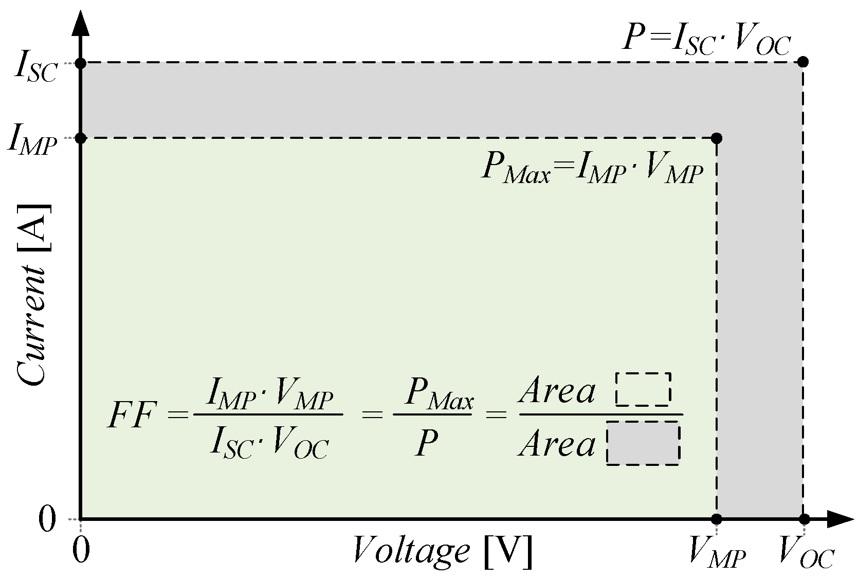
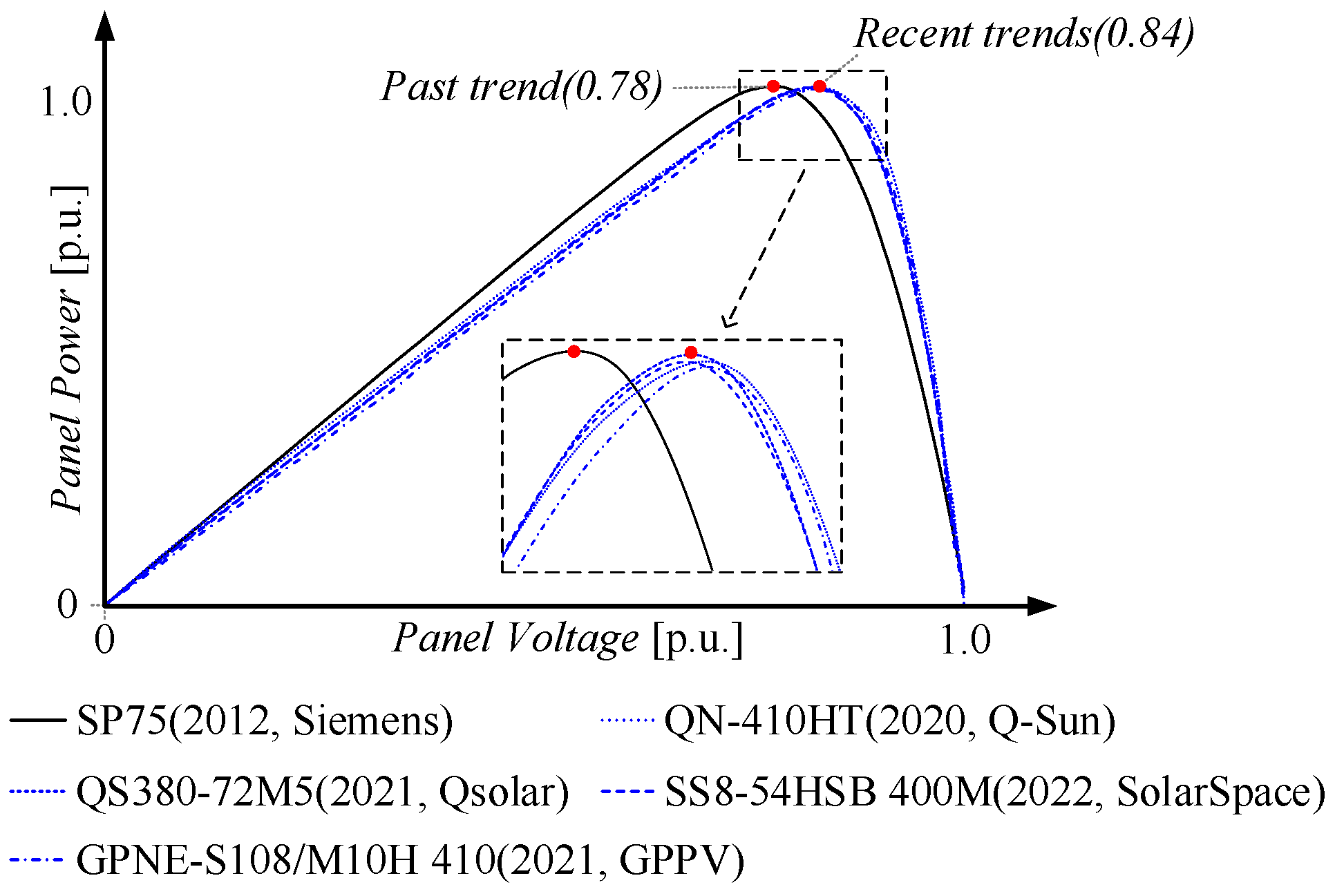
2.1. Characteristics of a PV Cell

Prior to designing a diode-type PVE, the characteristics and performance of a PV panel must be understood. In general, the fill factor (FF) and diode ideality factor (a) values are outlined, to determine and compare PV panel performances [28,29]. First, the FF value that represents the quality of the PV panel is, in theory, the rate of the maximum achievable power of the PV panel. Figure 1 shows the grey area determined using ISC and VOC, and the green area determined using the maximum current (IMP) and maximum power voltage (VMP). Their ratios, according to (1), can be expressed as the FF. Depending on the components that constitute the cell, this rate can reach approximately 80% for silicon cells and 89% for GaAs cells. However, the FF only represents the quality according to the type of solar panel and does not reflect the latest trends of the cell diode properties that the PVE intends to imitate. Moreover, the FF is not directly related to the power diode property curve.
F F = I M P V M P I S C V O C = P M a x I S C V O C
Second, the diode ideality factor (a), also referred to as the emission factor, is included in the numerical formula for determining the diode current, as shown in (2). This factor accounts for the electron–hole recombination and impacts the trend of the I–V property curve.
I D = I 0 [ exp ( V D a V t h ) 1 ]
Here, ID is the current that flows across the diode, I0 is the diode saturation current, VD is the voltage applied across the diode, a is the diode ideality factor, and Vth is the thermal voltage. Figure 2 shows the changes in the I–V property curves for different magnitudes of a. However, this value is entirely empirical and is not appropriate for analyzing the characteristics of PV cells in commercial products; instead, it acts as a variable during the selection of an equivalent diode parameter or is used to generate the LUT of the PV cell diode.
In this article, we studied various PV panels to obtain a standard for the PVE and discovered that the P–V property curve trend has recently changed. To intuitively compare the trends of the studied P–V curves, the curves were reconstructed after conversion using the p.u. law, as shown in Figure 3. The cell diodes of the selected panels were all monocrystalline, so it was assumed that there were no differences according to the panel’s characteristics.
In this paper, we defined the VOC to VMP ratio as Vrate, which was treated as a reference for comparison.
V r a t e = V M P / V O C
Figure 3 shows that Vrate = 0.78 for a previous SP75 (2012 year, Siemens) device. The value for more recent panels sold on the PV market (2020 year to 2022 year) is 0.84, which is a relatively higher number, hence a rightward shift was observed. We considered this trend in the P–V property curve and reflected this in the design process of the proposed PVE.

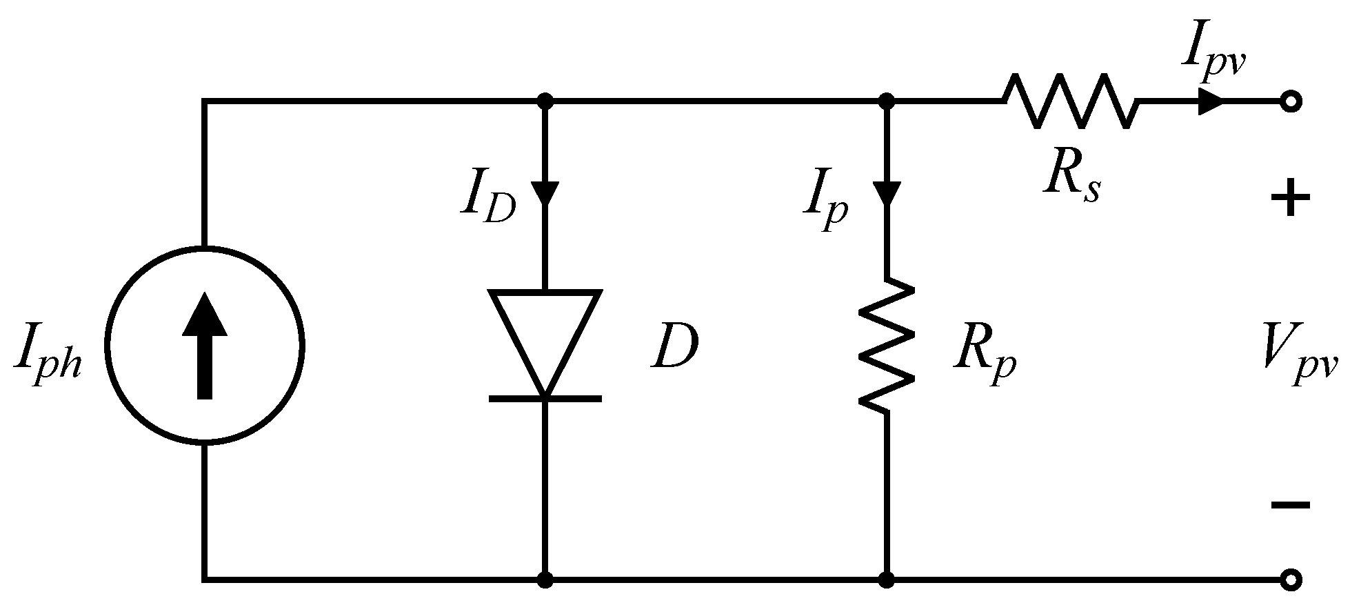
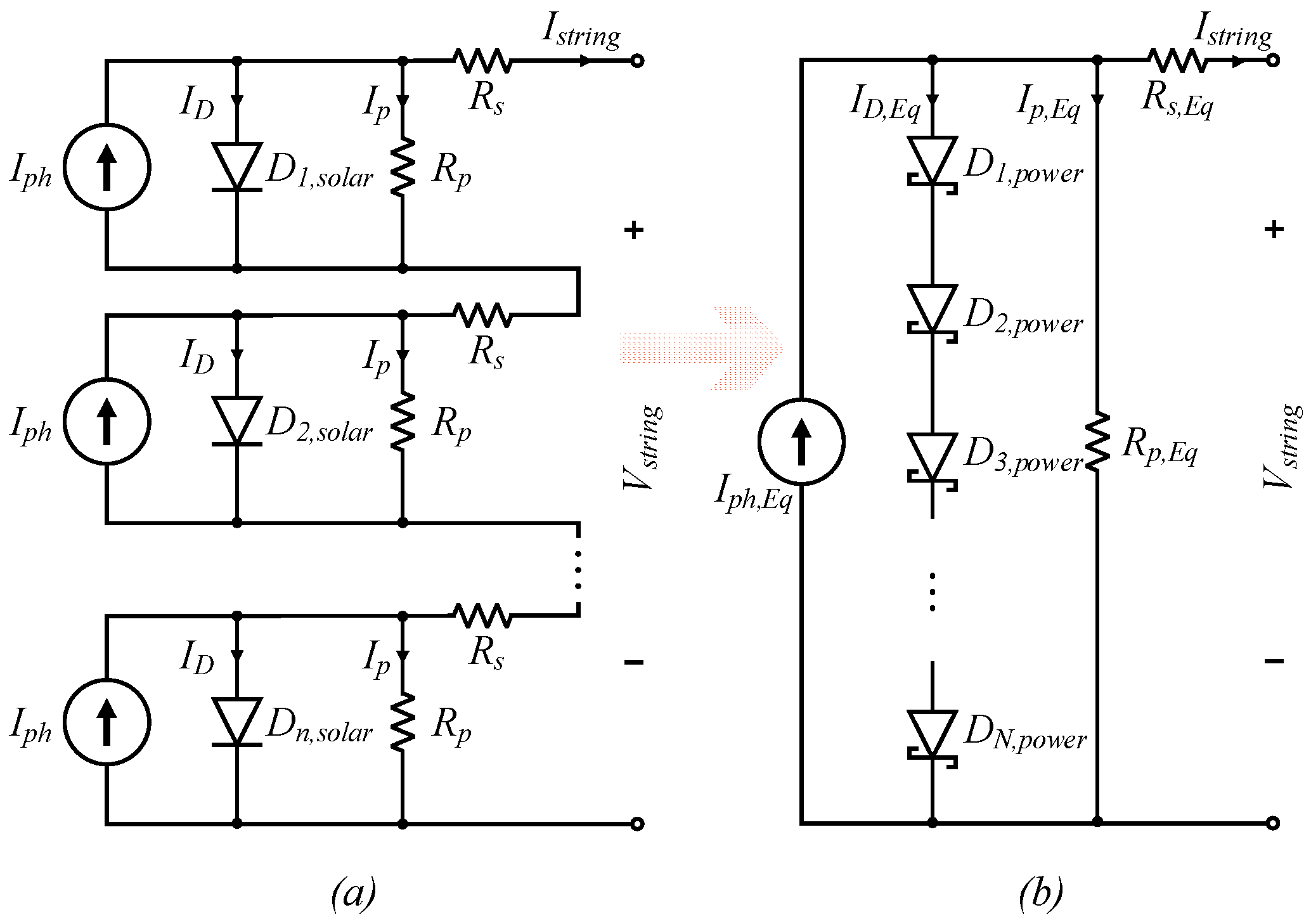
2.2. Equivalent Circuit Model of a PV Cell

The PV cell is the smallest unit in the composition of a PV system. To date, studies have presented various mathematical models of PV cells, among which one-, two-, corrected two-, and three-diode models are the most frequently cited [30,31]. In emulating a PV cell, overcoming nonlinearity, and representing this in an equivalent circuit with a diode, a two-diode model can be used to improve the accuracy of the imitation. In general, the use of a two-diode model that reflects seven parameters (Iph, I01, I02, a1, a2, Rs, and Rp), instead of the five (Iph, I0, Rs, Rp, and a) of a one-diode model, can increase the modeling accuracy. Here, Iph is a constant current source, Rs is the series resistance, and Rp is parallel resistance. However, the required controller specifications are cumbersome and the computation is time-consuming.
A two-diode model PVE composition has been adopted in the converter-type approach [21] and amplifies the signal level of the diode characteristic curve as a reference. Therefore, when selecting the signal level of the diode, a two-diode model can be implemented to improve the accuracy as much as LUT. Recent research [30] stated that I–V and P–V property errors depend on the number of diode models. However, it specified that minor errors are only found at low-irradiation levels in thin films. Therefore, the impact is not significant. Additionally, the I–V and P–V curves of the monocrystalline and multicrystalline cells that apply the latest PV cell technologies, which we consider in this paper, fall within a reasonable range (not exceeding 3%), regardless of the number of diode models. Furthermore, numerous papers [26,29] have studied how to improve the accuracy of the parameters of PV cell diodes and reduce the number of parameters. However, their approaches did not align with the considerations of this paper.
In this study, we did not intend to accurately determine parameter values to use as PVE reference signals but instead to construct a PVE through an actual power diode connected in series. Therefore, a two-diode model that requires the estimation of various complex and precise parameters is not necessary. Instead, one power diode selection is sufficient because it is widely used and simple in structure. Figure 4 shows the equivalent circuit model of a one-diode PV cell.
One-diode PV cells provide a significantly low current at a low output voltage of 0.5 V to 1.0 V. Suitable current and voltage values can be obtained by using 60, 72, and 92 PV cells in series. The shape of the PV output curve does not change due to the multiple PV cell connections, but the ISC and VOC values increase. Two or more PV cells or modules connected in series are referred to as a string. The detailed relation of string current, Istring, is presented in [30,31] and the result is as follows:
I s t r i n g = I p h I 0 { exp ( V p v + I p v N s R s N s n V t h ) 1 } V p v + I p v N s R s N s R P
Here, Vpv is the PV cell output voltage, Ipv is the PV cell output current, and Ns is the number of connections in series. Rp and Rs significantly impact the PV curve trend. This is covered in detail in Section 2.3. Figure 5a shows a PV string circuit, where the lower letter (n) and capital letter (N) signify the number of diodes before and after transformation, respectively. The corresponding circuit was reconstructed using the Norton equivalent, where n constant current sources were combined into a single constant current source (Iph,Eq), n PV cell diodes were transformed into N power diodes (D1-DN), and N series and parallel resistances were integrated into one each (Rs,Eq and Rs,Eq). Figure 5b shows the reconstructed circuit, and (4) can be simplified as in (5).
I s t r i n g = I p h , E q I D , E q I p , E q
Here, Iph,Eq is the Norton equivalent constant current source, ID,Eq is the current across the Norton equivalent diode, and Ip,Eq is the current across the Norton equivalent series resistance.

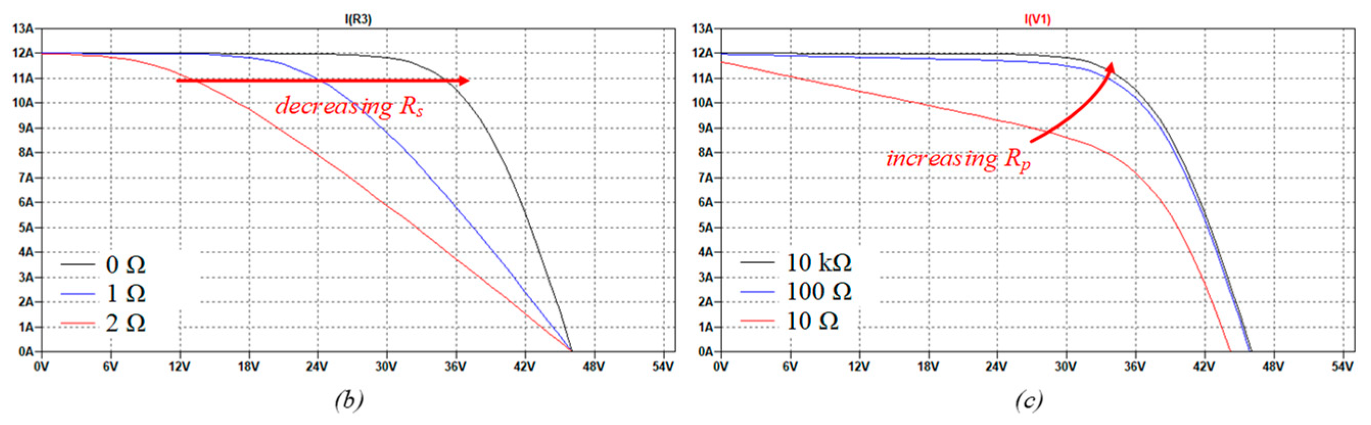
2.3. Impact of Rs and Rp on PVE

The use of five parameters was evaluated in a one-diode model. After the selection of diodes for a power diode PVE, Rs and Rp were the only controllable parameters. Numerous studies have discussed the impact and selection methods of Rs and Rp. In [32], the parameters of a diode model were extracted based on manufacturer datasheet parameters. This can be a simple method; however, it must have a detailed datasheet. In addition, neglecting the temperature dependency of resistances can diminish the accuracy, and the initial value should also be well designed. Therefore, this study followed the PV panel curve trend (Figure 3) regarding Rs and Rp as controllable factors, instead of calculating these resistances. The magnitudes of Rs and Rp were adjusted to various values, to identify the trend of the PV curve. Based on simulation, the magnitudes of Rs and Rp could be estimated to match the desired PV curve. Then, the actual resistances were determined during the experiment. The VOC circuit is open and is not impacted by Rs as the current across the resistance becomes 0. By deviating from VOC, the current starts to flow through Rs, changing the I–V curve properties of the PV cell.
Figure 6 shows that the point of Vrate tended to increase when Rs had a small value, which corresponds to recent trends. While the Vrate decreases as Rs increases, Vrate was approximately 0.5 when Rs was sufficiently large. As such, the I–V curve of the PV cell was significantly impacted by even the slightest change in Rs. In this study, we pursued a high value of Vrate; therefore, the value of Rs was considered as 0 or nearby. In contrast to Rs, the Vrate tended to increase when the Rp value was large, as shown in Figure 7. In addition, an unnecessary power loss was induced by providing an alternative current path to the Rp for the current generated from the PV panel. Therefore, a large Rp was preferred in this study.

3. Hardware Design of PVE

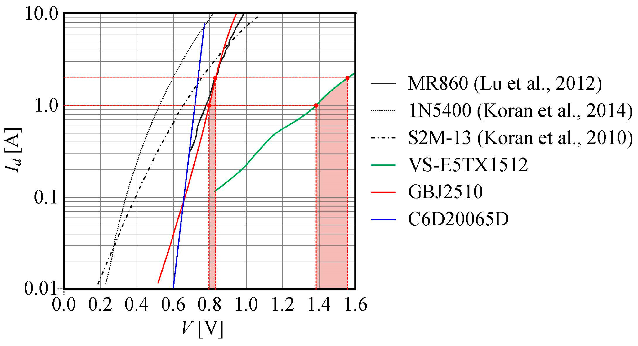
3.1. Diode Selection for PVE
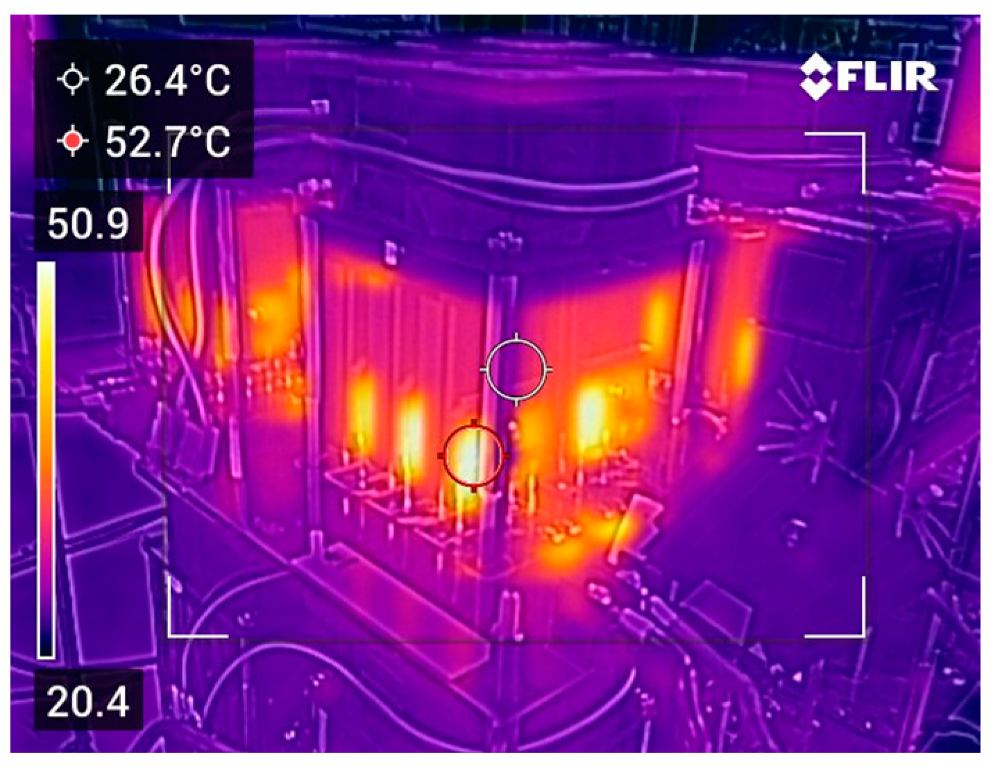
Figure 5 demonstrates that the PVE cell diode can be replaced with an actual diode, to constitute a circuit. Instead of the diode signal levels used in previous studies [1,24,25], the proposed PVE uses a power diode to increase the power capacity.
Figure 8 compares the forward bias and current of the selected diodes. The black lines represent the diodes used in previous studies. The main signal level diodes used were MR860 (fast recovery power rectifiers [25]), 1N5400 (general purpose silicon rectifiers [24]), and S2M-13 (surface mount glass passivated rectifier [1]). These diodes have a relatively low slope, which implies that a certain amount of increment in the current could lead to a relatively higher power loss. Due to the small available current in these diodes, a high-power PVE cannot be fabricated. Moreover, the thermal design is limited by the absence of thermal pads to attach the heat sink directly on the devices, such as in the 1N5400 and S2M-13.
A through-hole type power diode that has a thermal pad was considered appropriate for a temperature-resistant design. Three models were compared, to investigate the diode characteristics, and the most appropriate diodes were chosen for this study: the green (VS-E5TX1512), red (GBJ2510), and blue (C6D20065D) lines in Figure 8.
First, the VS-E5TX1512 (hyper-fast rectifier) could withstand up to 1200 V with a 15 A rated current; therefore, it could sufficiently handle the ISC (about 11 A) of a general 400 W panel. However, the slope of its I-V curve is significantly low, and the loss increases as the current increases. Therefore, this diode is not appropriate for the proposed PVE application. Figure 9 shows that the slope of the Id–V curve is relevant to the recent trend of PV cells. It can be noted that the I–V and P–V curves fundamentally originate from the Id–V curve. Therefore, in case of a higher slope in the Id–V curve, the recent technological state can be more accurately reflected in the PVE.
Second, the GBJ2510 is a highly credible and high-temperature-resistant glass passivated bridge rectifier. It uses a GBJ package type of 30 mm × 4.8 mm × 20 mm (W × L × H), which is broader than that of the available thermal pad of TO-247-3 (16.1 mm × 5.2 mm × 21 mm) that is mainly used in discrete-type diodes. Therefore, it is considered advantageous for thermal designs. Furthermore, the GBJ2510 has a bridge structure, which is composed of a 4-pin (+,~,~,-) terminal, among which the second and third pins are unused, and two diodes are used in series–parallel. In Figure 8, it can be seen that it is superior to the VS-E5TX1512 in terms of loss, because the slope of the Id–V curve is steep. In Figure 8, a difference in power can be observed when the current increased from 1 to 2 A, which allows for an intuitive comparison of the magnitude of the power loss.
Last, the C6D20065D (SiC Schottky diode) in CREE is an option which can support up to 650 V and 20 A, with 1.27 V of forward voltage drop. It is true that its slope is most suitable for this design; however, the unit price (online price: USD 8) was not favorable for the multi-diode composition adopted in this research. The package type was a commercially used TO-247-3, but its availability was limited, because only CREE supplies this diode. In contrast, the GBJ2510 can handle up to 1000 V and 25 A, with relatively high slope and a price advantage (online price: USD 2). Additionally, Comchip Technology, Panjit, Micro Commercial Components, and SMC Diode Solutions have products with identical names and specifications to those of the typical diode supplier Diode Incorporated, with facilitates the product supply. Therefore, in the proposed PVE, we selected the GBJ2510, which has sufficient stock and is cost effective for the designed hardware.

3.2. Thermal Design

This section introduces the design process for moderating the heat dissipation through the use of the power diode. Equation (6) determines the junction temperature [27].
T j = R t h , t o t a l P l o s s + T c o o l a n t
Here, Tj is the junction temperature, Rth,total is the total thermal resistance, Ploss is the power loss, and Tcoolant is the atmospheric temperature.
R t h , t o t a l = R t h , J C + R t h , T I M + R t h , C P
Here, Rth,JC is the thermal resistance from the junction to the case, Rth,TIM (TIM: thermal interface material) is the thermal resistance that links the case and heat sink, and Rth,CP (CP: cold plate) is the thermal resistance of the heat sink.
The GBJ-2510 (Diodes Incorporated) was selected for the hardware design. According to the data sheet [33], Rth,JC is 1 °C/W; however, this value was derived from as case with a 250 mm × 250 mm × 20 mm (W × L × H) heat sink. This dimension in the datasheet is large and restricted to ideal use; this heat sink volume cannot be applied to PVE design or to realistic values. Therefore, the heat sink had to be reselected through detailed thermal design and considering the hardware size, and the Rth,JC value had to be re-determined accordingly.
For the prototype, we considered a diode size of 30 mm × 4.8 mm × 20 mm and chose a heat sink (HSE-B20250-045H, 25.4 mm × 3.0 mm × 50 mm of CUI Devices) that was attachable to a single product. In this way, assembly was easy, and the total hardware volume and weight could be minimized, without a bulky heat sink. Based on the heat sink volume chosen for this study, and with reference to the ideal heat sink in the datasheet, the value of Rth,JC was determined to be 2.2 °C/W. A thermal grizzly Kryonaut was used and the value of Rth,TIM was 0.2 °C/W.
Rth,CP was calculated along with the heat sink selected above. In the case of air-cooling, the thermal resistance was plotted against the air-flow speed. A 12 V EC8038H12BA (80 mm × 80 mm × 38 mm) fan with an air-flow speed of 67.1 CFM was used to minimize the heat dissipation from the diode. Using Equation (8), the CFM air-flow speed needed to be transformed to 975 LFM to match the unit in [34]. The graph on the datasheet allowed us to determine a Rth,CP value of 2.0 °C/W.
L F M = ( 304.8 ) 2 C F M L W
P l o s s = I s c V o c D n
According to (7), Rth,total was determined as 4.4 °C/W. Based on (9), the power loss could be obtained. Here, the number of diodes Dn was set as 48. ISC and VOC were 12 A and 46.6 V, respectively. Finally, Ploss was calculated as 11. 65 W.
Tcoolant was the atmospheric temperature of the laboratory, which was set as 45 °C, as a moderate condition; generally, most studies use 25 °C, 45 °C, or 65 °C. The diode datasheet [33] indicates that the operating temperature is −65 °C to 150 °C. Finally, Tj was determined to be 96.26 °C, using (6) based on the values determined above. During experimental verification, the laboratory temperature was set as 25 °C, and Tj could be recalculated as 76.26 °C. The temperature of the heat sink of the diode could be obtained by modifying (7) according to each junction temperature; this was determined as 48.3 °C, which was decreased by 27.96 °C from 76.26 °C, Tj. In the experiments, the thermal design was validated by measuring the temperature of the heat sink during saturation testing.

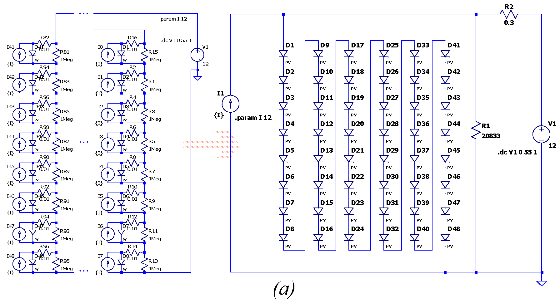
3.3. Simulation Configuration and Results

In this paper, the operation of the PVE was verified using LTspice, which is a Spice-based analog electronic circuit simulator software. It can more precisely adjust the characteristics of the diode model than other similar simulation tools. The diode model in Spice consists of 15 parameters representing the diode characteristics. Generally, the main parameters are as follows: saturation current (Is), ohmic resistance (Rs), zero-bias function capacity (Cjo), ideal factor (a), grading efficiency (m), and reverse breakdown voltage (Bv). Instead of using LTspice’s own library, the actual diode’s Spice model could be obtained through the diode manufacturer’s website, to enhance the accuracy of the results. As long as the main parameters are provided by manufacture, the remainder can be set to be default values without much impact on the results. The parameters constituting the Spice model of the GBJ2510 diode used in this paper are Is = 379 n, Rs = 2.84 m, Bv = 1.00 k, Ibv = 10.0 u, Cjo = 146 p, m = 0.333, a = 2.07, and Tt = 4.32 u. While, the C6D20065D diode that was compared in the diode selection process had a relatively small number of parameters, Is = 0.88 p, Rs = 0, Cjo = 0.1 p, and Bv = 779.
Referring to Table 1, the electrical characteristics of the PV module could be equivalently converted into the PVE model by replacing the PV cell diodes with the power diodes. The solar panel information in Table 1 was obtained from the ENF solar website [35], which provides datasheets of more than 70,000 solar panels. In this paper, the design requirement of the PVE was 400 W, therefore the PV cell diodes were set to 72, matching the VOC of 49.4 V (see Table 1). Finally, based on the simulation results, the number of power diodes was determined to be 48. Consequently, the accuracy could be improved and we could avoid a trial-and-error simulation before moving on to the actual hardware design. As an advantage of the proposed PVE, the desired VOC can be easily obtained by adjusting the number of diodes in hardware. The summation of diode forward voltages is the VOC.
Figure 10a shows the equivalent conversion of the PV cell diode model to the power diode model in LTspice. The value of the constant current source is not changed, Rs can be calculated by multiplying by the number of diodes, and Rp can be calculated by dividing by the number of diodes. Figure 10b,c show the simulation results of the I–V property curves according to Rs and Rp, respectively. These results were matched with Figure 6 and Figure 7. It can be seen that the maximum Vrate of the corresponding diode was maintained when Rp was 10 kΩ or above.

3.4. Hardware Implementation of the 400 W PVE

In this paper, a 400 W PVE was built, and its actual configuration is shown in Figure 11. It consisted of a DC power supply operating in constant current mode, 48 series-connected power diodes (GBJ2510), series resistors (Rs), parallel resistors (Rp), and eight cooling fans operating through external power sources, to control the heat of the diodes. Each cooling fan was designed to handle six diodes, considering not only the window of air flow but also the maximized effect of wind speed. As a result, the overall power density could be optimized using the selected diode and heat sink.
In this PVE hardware PCB design, the total length of the trace is expressed in the form of resistance, since multiple diodes are connected in series in the layout. Therefore, in the PVE model of Figure 11, the equivalent resistance Rs is equal to the sum of Rs,trace (by PCB trace) and Rs,add (by external connection, if it is needed).
As analyzed earlier, Rs is a function of power loss and also affects the slope of the PV curve. In order to minimize the influence of Rs,trace within the PVE, the length of the trace needed to be minimized. When it was necessary to adjust the size of Rs during the test, it could be simply configured by adding Rs,add to the output terminal of the PVE. The length of the trace was designed with the minimized length, using the measurement function of the PCB. Finally, the value of trace was confirmed as 2743.5 mm. The equivalent resistance Rs,trace could be calculated by substituting the obtained trace length and parameters into (10). The designed value of Rs,trace of this PVE was calculated as 160 mΩ (148 mΩ at 25 °C).
R s , t r a c e = R L A ( 1 + ( T e m p _ C o ( T e m p 25 ) )
where R is the resistivity (copper: 1.7 × 10⁻⁶), L is the length (2743.5 mm), A is the area (thickness, 4.5 mm × width, 0.07 mm), Temp_Co is the temperature coefficient of the material (copper: 3.93 × 10⁻³), and Temp is the temperature (45 °C).
In order to simulate the actual situation of a PV panel installed outdoors, the partial shading effect should be considered in the PVE. Partial shading occurs in PV panels due to various causes, such as clouds, trees, buildings, pollution, snow, and animal waste [36,37].
The proposed PVE can easily implement the case of partial shading using multiple series connections. Figure 12 shows the experimental configuration when the individual PVE had multiple series connections. Three PVEs were connected in series to form one string, and partial shading tests could be easily performed by adjusting the value of the current source of each PVE. For example, the case of connecting three PVEs (A, B, and C) in series was as follows: If the constant current source of PVE A was set to 10 A, PVE B and C were set to 5 A and 2 A, respectively. This could emulate the partial shading effect as found in the actual case of a solar panel. Assuming that the current flowing to the load is gradually increased from 0 A, the entire PVE operates up to 2 A, and when it exceeds 2 A, PVE C is bypassed. Subsequently, PVE A and B operate simultaneously until 5 A; when 5 A is exceeded, PVE B is also bypassed, and only PVE A operates up to 10 A. In this way, several maximum power points (MPPs) exist through multiple series connections, where partial shading produces global and local MPPs. The detailed experimental results of multiple series connections are discussed in the next section.
In the general converter-type PVE, its operation and configuration do not consider multiple series connections when only applying a single control circuit. On the other hand, the diode-type of PVE proposed in this paper used the diode’s own characteristics, so even if several PVEs are connected, smooth operation is feasible, without additional control. Therefore, the number of PVEs connected in series can be configured in a flexible way according to the desired current, voltage, and power ratings. In addition, an individual PVE can use a different type of power diode, without restrictions when multiple series of connected PVEs are required, to investigate partial shading. The diode characteristic curve can be specifically adjusted using Rs and Rp, so there is flexibility in the system configuration. The ultimate purpose of the PVE is integrated operation with the power optimizer (also known as the dc optimizer), which can increase the output power of the solar panel. The proposed PVE seamlessly operates with the power optimizer tracking the MPP. In Figure 13, the x-axis and y-axis represent 24 h and the output solar power, respectively.
When a solar panel (black solid-line) is operating alone, the output power is high at noon when the level of sunlight is high as well. When the power optimizer is connected (blue dot-line), the MPPT operation increases the solar power output. Detailed results are shown in the experiment section.

4. Experiment Results

In this paper, various experiments were performed to evaluate the performance of the PVE prototype.

4.1. Experiment Configuration of Proposed PVE

Figure 14 shows the hardware setup for the testing of the proposed PVE. It consisted of a 400 W dc power supply (operating in constant current mode), 12 V dc power cooling fan, 400 W electronic load to flow current, and the PVE prototype.
Figure 15 shows a block diagram of the experimental process of the proposed PVE, showing the partial shading and load changing conditions. As the main power components, there were three DC power supplies (PS) that were operated in constant current (CC) mode, three PVEs, and an electric load. This block diagram shows the multiple series connections for testing partial shading; moreover, it could be configured as a single DC PS and PVE for simple testing. In the commends block, the partial shading signals were sent to the DC-PS to change the CC commends. Meanwhile, the load change signals were sent to the electric load, to test the transient response. Using the measurement block, the values of the voltage and current at the input and output were acquired. Based on these data, the I–V curve was first obtained, and then it could easily be converted into the P–V curve.

4.2. Effect of Additional Rs on I–V and P–V Curves

Figure 16 shows the experimental results comparing the I–V and P–V curves, according to the values of Rs,add, which had a great influence on the tendency of the PVE. On the other hand, based on the simulation results, the magnitude of Rp was found to be higher than 10 kΩ. In addition, the sufficient value of Rp (>10 kΩ) did not have much impact on the I–V curve. Therefore, the impact of Rs is mainly studied in this section.
During testing, the input current source was fixed at a constant current of 12 A, while the electronic load was changed from 0 A to 12 A. Besides Rs,trace, which was affected by the design of the PCB trace, various different values of Rs,add were externally connected to investigate their effects. In the designed prototype, screw-type terminals were used for easily changing of the resistance. Moreover, cement resistors were preferred, considering their power rating. Based on the analysis in Section 2.3 and the simulation results (small Rs was preferred), the four comparative models were tested at 0 Ω, 0.1 Ω, 0.2 Ω, and 0.3 Ω. As shown Figure 16a, the I–V curve moved to the bottom left side, indicating a smaller Vrate with a higher Rs,add. Similarly, the maximum output power of the PVE also decreased with a higher Rs,add, as shown Figure 16b. It can be noted that trivial changes of Rs had significant effects on the PVE characteristics in terms of the I–V and P–V curves. Therefore, the proposed PVE design used a smaller value of Rs to ensure a higher Vrate and a decreased power loss.

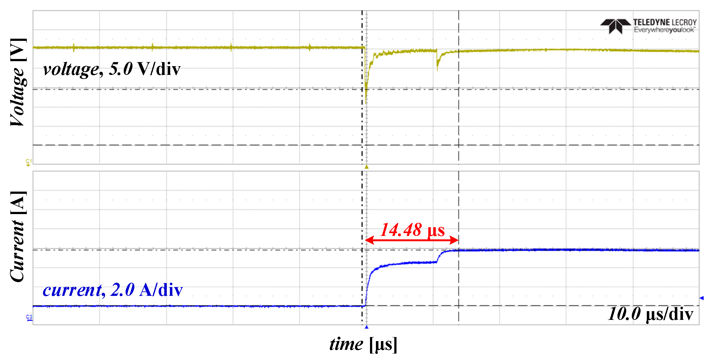
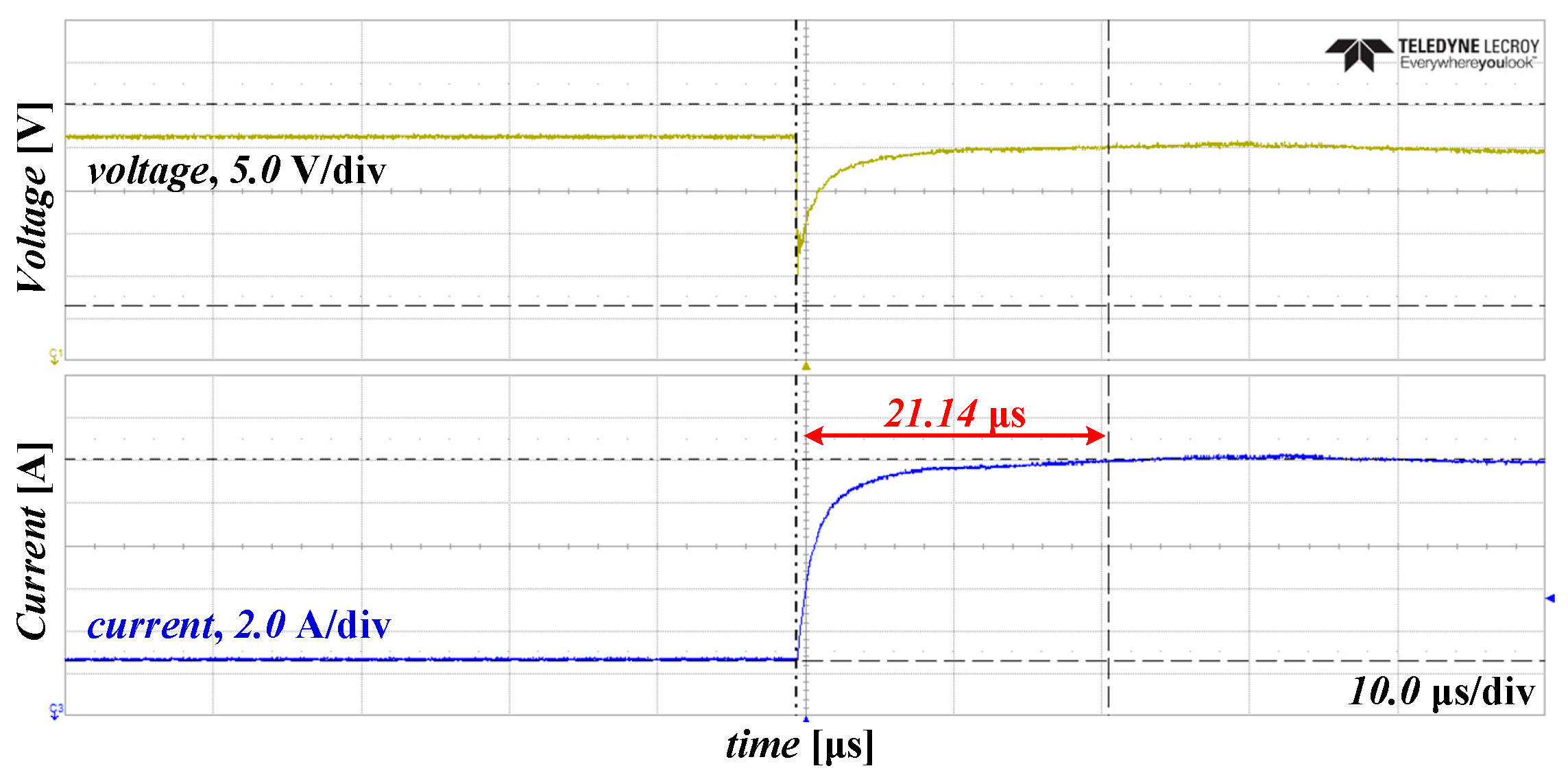
4.3. Dynamic Response

The purpose of this test was to validate the response speed of designed PVE when the magnitude of the resistive load or irradiance (W/m2) on the PV panel had step changes.

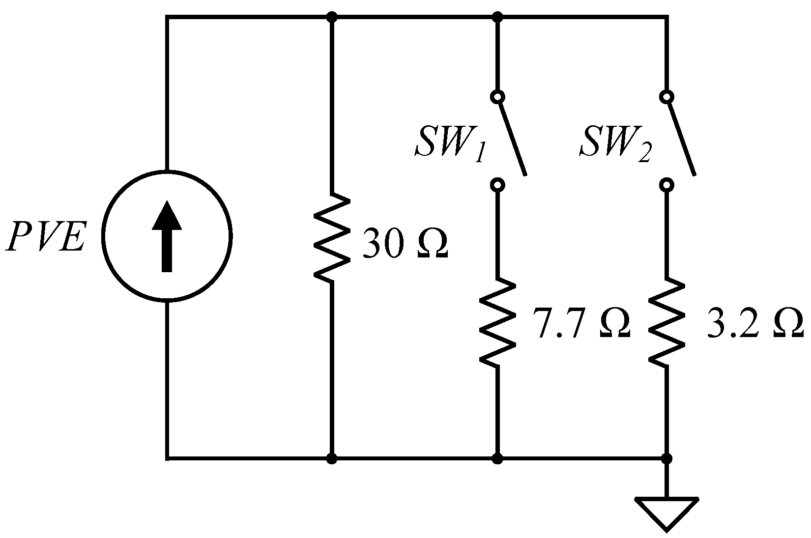
4.3.1. Experiment Results of Step Changes in the Resistive Load

A load variation experiment was necessary, to validate the performance of the MPPT algorithm. In short, as the control speed of the MPPT converter is improved, the fast response of the PVE must be guaranteed for testing various MPPT algorithms [38]. Figure 17 shows the configuration of the resistive load with switch relays and the resistances. According to each step, the values of resistance, current, and power are summarized in Table 2. Here the switch relay, JER-E2S D32 (32 A) was utilized to achieve a fast response and for safety.
Figure 18 shows the dynamic response when switching from step A to step B in Case1. In this step load change from 30 Ω to 6.2 Ω, the current increased by 5 A. The response time was very fast, with Δt = 14.48 μs, and the voltage changed as quickly as the current. Figure 19 shows the results of Case 2 (from step B to step C). The resistance was changed from 6.2 Ω to 2.2 Ω, and the current increased from 1.5 A to 6.5 A. The response time was Δt = 21.14 μs, showing an excellent performance as in Case 1. Figure 20 shows the result of Case 3, switching from step C to step B. The value of the resistor had a step change from 2.2 Ω to 6.6 Ω, and the current decreased by 5.5 A. In Case 2, the switching was performed at once, and the response time was also fast, being Δt = 19.20 μs. As a result, the dynamic response of the proposed PVE was less than 22 μs, regardless of the rising time and the falling time. It can be seen that the response speed was very fast for this prototype compared to the experimental results of conventional converter-type PVE studies of 200 μs [11], 3.8 ms [1], and 29.6 ms [10].

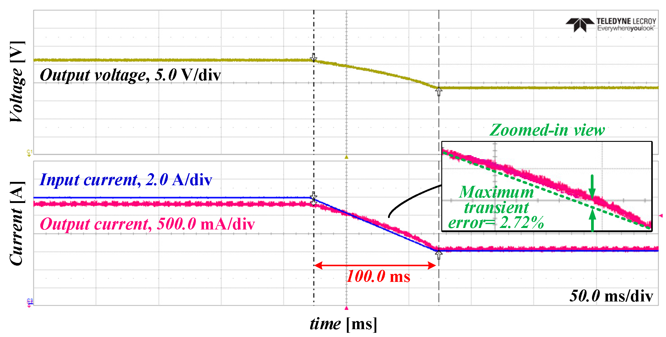
4.3.2. Experiment Results of Dynamic Response in Input Current

The rapid response of an PVE is important when the partial shading effect needs to be emulated. This can be tested through step changes in the current source, representing rapid changes of irradiance. Instead of using the electronic load of Section IV-B, pure resistive loads were used to verify the dynamic response, avoiding interference by the other circuity within the electronics load. To investigate the response time when changing the input current of the PVE, the load was fixed at 6.2 Ω, and the input current was reduced from 12 A to 6 A.
Here, the DC power supply could adjust the current reference (input current) to 100 ms, as the minimum transient speed in constant current mode. Figure 21 shows the good performance for the dynamic response, where the output current (pink trace) tracked the input current (blue trace) at almost same speed. In terms of accuracy, the maximum transient error was calculated as 2.72% during the partial shading condition.

4.4. Efficiency of PVE

The efficiencies of the MPPs of the PVE prototype were measured according to certain values of Rs,add. In detail, the constant input current was set to be 12 A, while changing the values of Rs,add from 0 Ω to 0.3 Ω. Referring to Table 3, it is obvious that the highest efficiency (91%) was obtained with the lowest value of Rs,add (0 Ω) because of its power loss. Figure 22 shows the relation between the input power, output power, power loss, and efficiency of the PVE according to the voltage Rs,add = 0 Ω, but this was not an ideal case because the imbedded Rs,trace was 0.16 Ω.
The input power (Pin) increased linearly as the voltage increased, and the output power (Pout) reached the maximum value at 35 V (VMP) and then decreased gradually along with the P–V curve and the power loss (Ploss) increased accordingly. The efficiency of the PVE gradually increased as the voltage was decreased. In the range where the voltage was less than 35 V, the current flowing to the PVE became very small and this is not a general operational point of the experiments. Therefore, the system efficiency was 91% at 35 V, near the MPP. When the proposed PVE was integrated with the MPPT converter, to verify the performance of its maximum output power capability, the main operating point of the PVE was near the MPP. Therefore, the efficiency in this area was, not only very important, but also acceptable.
Figure 23 shows the effectiveness of the PVE prototype regarding heat dissipation in continuous operation for 1 h. In this test, the temperature of the laboratory was maintained at around 25 °C to 27 °C, and the maximum heat point obtained was 52.7 °C. Based on the thermal design, the error was maintained 5.0 °C below the calculated value, at 48.3 °C.

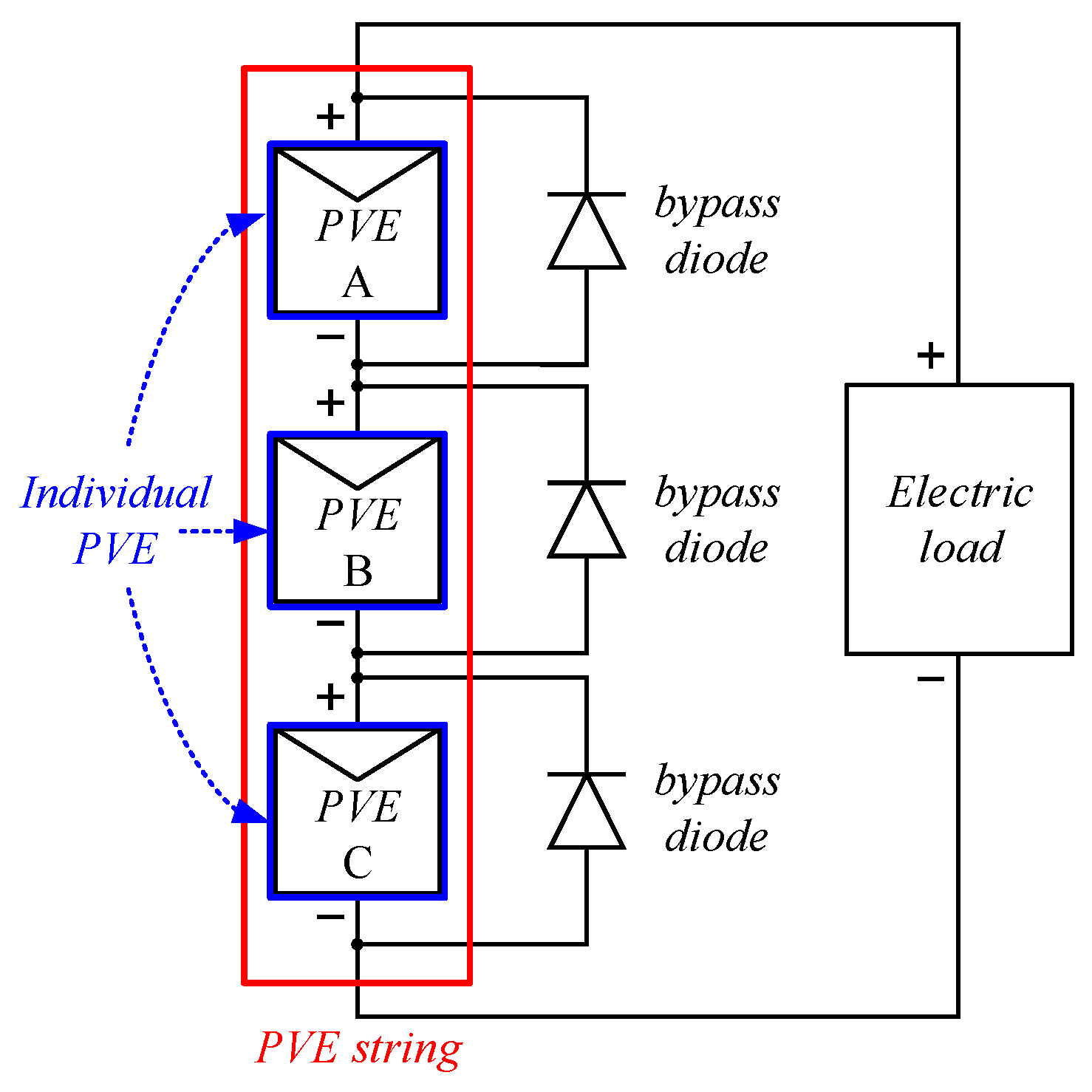
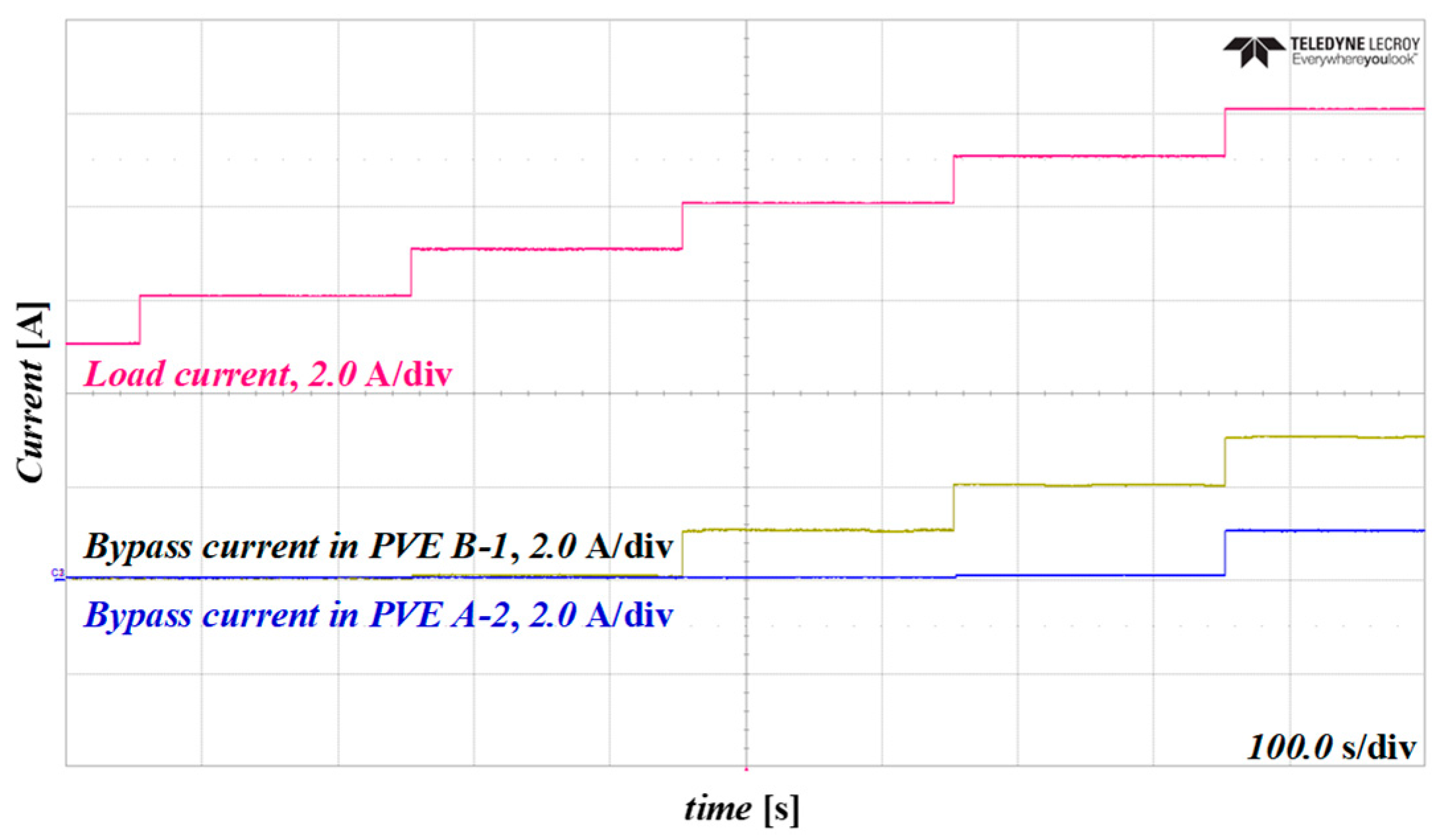
4.5. Verification of Partial Shading Operation through Multiple Series Connections

In order to investigate the partial shading effect, three PVEs were connected in series to form one string, and both ends of the string were connected to the electronic load, as in Figure 12. An additional bypass diode was connected to each PVE output, to prevent a current bottleneck. Partial shading was simulated by varying the magnitude of the current source of each PVE.
In traditional converter-type PVE studies [39], an additional active switch, current sensor, voltage sensor, and PI controller are required in multiple series connections. In [13], an actual light source (0.5 W) and analog circuit based real-time reference generation circuit were necessary to extract the I–V curve, and it had to be further digitally processed.
Multiple series connections require creating an accurate I–V curve that includes the characteristics of partial shading. There are three of representative ways of implementing this: (1) Add a new light source(s). (2) Change the parameter values in the analog circuit. (3) Digitally change or create a new LUT. However, these methods introduce the following problems: (1) Bulky hardware system. (2) Increased design complexity in the analog circuit. (3) Time delays and increased computational time for the digital control.
The main advantage of the proposed PVE is the flexibility in its configuration, and this has a benefit when the partial shading effect is tested. The number of multiple series connections in the series of PVE can be adjusted according to the rated power and the particular level of partial shading effect. In addition, the different specifications of power diodes that have been separately designed can be properly tied in multiple series connections without an issue.
During the partial shading experiments, two types of PVE models (PVE A: GBJ2510 and PVE B: VS-E5TX1512) were utilized in multiple series connections. This configuration helped to validate the flexibility of proposed PVE when it used power diodes with different characteristics. Table 4 summarize three cases of multiple series connections for the partial shading experiment. The main operating characteristic followed PVE A, because the highest input current was allocated to PVE A-1 for all cases.
The experimental results are summarized in Table 5.
Case 1 represents the state of the same irradiances, without partial shading, and identical currents of 9 A were allocated to the three PVEs. Looking at the P-I curve (black line) in Figure 24a, only one global value of MPP appears, as if single PVE was operated. Figure 24b also shows the shape of the I–V curve (black line), without sudden current fluctuations, as in the operation of a single PVE.
Case 2 was a state where A-1 had no shading and A-2 and B-1 had partial shading. A-1 was set to 10 A, and A-2 and B-1 were set to 9 A and 7 A, respectively. Referring to the blue line in Figure 24a, three MPPs occurred as global values at 6 A and local values at 8 A and 9.8 A. When the current flowing to the load became higher than the input current of the PVE, the corresponding PVE was bypassed. Referring to the blue line in Figure 24b, it can be seen that the inflection points (local MPP) occurred at 9 A and 7 A.
Case 3 was a state where partial shading occurred only in A-2 and B-1, as in Case 2, and the input current was changed to 7 A for A-2 and 5 A for B-1, emulating a more severe shading case. Referring to the red line in Figure 24a, the global and local values appeared as different shapes from Case 2. It can be seen from the red line in Figure 24b that the inflection points occurred at 7 A and 5 A. In terms of partial shading, the local and global MPPs appears as the graphical curves in Figure 24 through multiple series connections.
The currents flowing into the output (load) and bypass diode were investigated, to verify the proper operation of the multiple series connections and to describe the operational principle. Thus, the experimental waveforms were obtained as seen in Figure 25 over a substantial period of time, and this test was associated with Case 2, as seen above when obtaining the curves for Figure 24. In this experiment, an output current of 5 A flowed through the electronic load as an initial condition. During the test, the load current was increased by 1 A as a step change every 200 s. Until the current reached at 7 A, all PVEs operated in the normal mode, without bypass operation. When it reached 8 A, the bypass diode of the B-1 model started to operate, and a current of 1 A that exceeding the input current of 7 A flowed through the bypass diode. When it became 9 A, the bypass current of the B-1 model increased to 2 A. When it reached 10 A, the bypass diode of the A-2 model also started to operate, and the 1 A exceeding the input current of 9 A in the A-2 model was bypassed. Through this experiment, it was confirmed that partial shading operation can be simply implemented using multiple series connection of several PVEs, without additional controls and devices.

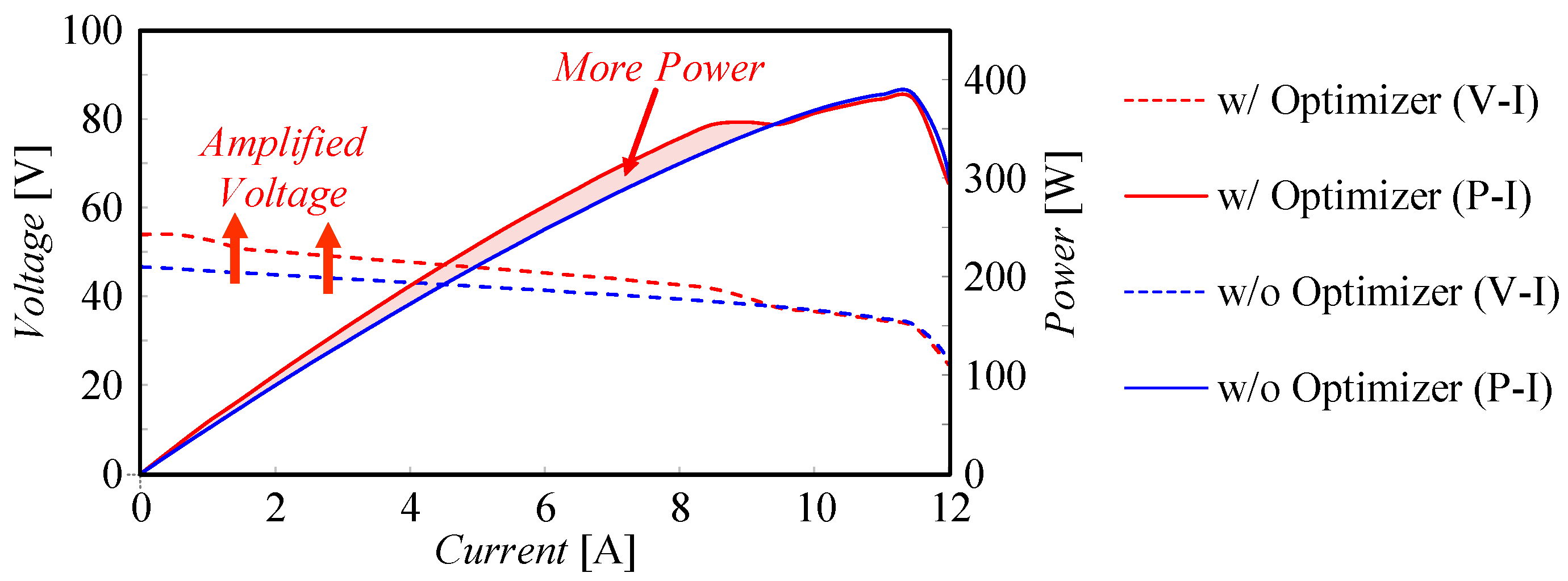
4.6. Integrated Operation with the Power Optimizer

Due to the nonlinearity of the PV system caused by changing the irradiation and temperature, the MPPT algorithm was employed to attain the maximum power production. This algorithm measured the voltage and current of the PV array and tracked these variations in the MPP to obtain the maximum efficiency from the PV, such as in the perturb and observe (P&O) method in [40,41]. To verify the integrated MPPT operation, the proposed PVE and the power optimizer of SolarEdge’s P400 (P&O method, [42]) were utilized. Referring to Figure 26, the x-axis represents current, and the main and auxiliary y-axes represent the voltage and power, respectively. The red area of the P–I curve indicates that increased power (red line) was achieved using the power optimizer when the current was below than 9.3 A. The power optimizer (buck-boost converter) could amplify the voltage, to produce a constant power in the low current region. It can be noted that the integrated operation between this optimizer and the proposed PVE was demonstrated and the performance of the power optimizer was validated.

4.7. Comparative Investigation with Commercial PVEs

For a comparative investigation, PVE commercial products from Chroma (62050H-600S) [43] and Elektro-Automatik (EA-PSI 9500-06) [44] were compared based on their datasheets. In terms of the transient response time, the proposed PVE had the fastest response, of 22 μs, compared to the Chroma and Elektro-Automatik PVEs, 1ms and 30 ms, respectively. In terms of efficiency, the proposed PVE achieved 91%, which was much higher than the Chroma PVE (87%) and slightly lower than Elektro-Automatik PVE (93%). Generally, the commercial PVEs offered two modes to generate the PV characteristic curve [43,45]. A parameter-based mode used four points (open-circuit voltage, short-circuit current, and voltage and current at the maximum power point) to simulate I–V characteristic outputs. This not only produces an extremely simplified curve, obtained with particular points, but also leads to the simulating only two slopes of a single characteristic curve. Meanwhile, the table mode can define the curves in the form of a point array using a user-programmed voltage and currents. This might be more precise than the parameter-based mode. However, its accuracy is also limited by the memory size, and it is slower than the first mode. This is the reason why the proposed power diode-based method showed the fastest response compared to the commercial ones.

5. Conclusions

A simple, fast-response-time, flexible, and reliable 400 W photovoltaic emulator (PVE) with series-connected power diodes was proposed. Investigating the characteristic of the diode and its equivalent circuit model for PVE, design procedures, including power diode selection, thermal design, and simulation methods were introduced. Compared to converter-type PVEs, which can be sensitive to sensors, require complicated analog circuits, and generate time delays caused by digital controls, the proposed PVE can be simply implemented, achieving good dynamic performance with a reduced cost. Moreover, it has the flexibility to reconfigure the number of power diodes when the commercial solar power product has different specifications. In consequence, unlike the conventional research on diode-type PVE using a series arrangement of signal diodes that only carry several tens of watts, the prototype PVE can successfully implement up to 400 W, with 91% system efficiency at near the MPP, and without heating problems. Using multiple series connections of individual PVEs, it is possible to emulate the actual environmental conditions. During the partial shading test, the PVE showed a good performance, indicating local/global MPPs. In the integration test with a power optimizer, an increased output power was obtained by evaluating the MPPT algorithm.

Author Contributions

Conceptualization, S.P. and J.H.; methodology, S.P. and J.H.; software, S.P. and S.C.; validation, S.P. and J.H.; formal analysis, S.P. and J.W.; investigation, S.C. and J.W.; resources, S.C. and J.W.; data curation, S.C. and J.W.; writing—original draft preparation, S.P. and S.C.; writing—review and editing, J.W. and S.C.; visualization, S.C. and J.W.; supervision, S.P. and J.H.; project administration, J.H.; funding acquisition, J.H. All authors have read and agreed to the published version of the manuscript.

Funding

This research was supported by Technology Development Program to Solve Climate Changes through the National Research Foundation of Korea (NRF) funded by the Ministry of Science, ICT (2021M1A2A2065441), and in part by the Gachon University research fund of 2022(GCU-2019-0778).

Data Availability Statement

Not applicable.

Conflicts of Interest

The authors declare no conflict of interest.

References

  1. Koran, A.; Sano, K.; Kim, R.-Y.; Lai, J.-S. Design of a photovoltaic simulator with a novel reference signal generator and two-stage LC output filter. IEEE Trans. Power Electron. 2010, 25, 1331–1338. [Google Scholar] [CrossRef]
  2. Koutroulis, E.; Kalaitzakis, K.; Voulgaris, N.C. Development of a microcontroller-based, Photovoltaic Maximum Power Point Tracking Control System. IEEE Trans. Power Electron. 2001, 16, 46–54. [Google Scholar] [CrossRef]
  3. Huang, Y.; Shen, M.; Peng, F.Z.; Wang, J. Z-source inverter for residential photovoltaic systems. IEEE Trans. Power Electron. 2006, 21, 1776–1782. [Google Scholar] [CrossRef]
  4. Chen, Y.; Smedley, K.M. A cost-effective single-stage inverter with Maximum Power Point tracking. IEEE Trans. Power Electron. 2004, 19, 1289–1294. [Google Scholar] [CrossRef]
  5. Quan, L.; Wolfs, P. A review of the Single Phase Photovoltaic Module Integrated Converter topologies with three different DC link configurations. IEEE Trans. Power Electron. 2008, 23, 1320–1333. [Google Scholar] [CrossRef]
  6. Padmanaban, S.; Priyadarshi, N.; Bhaskar, M.S.; Holm-Nielsen, J.B.; Hossain, E.; Azam, F. A hybrid photovoltaic-fuel cell for grid integration with Jaya-based Maximum Power Point Tracking: Experimental Performance Evaluation. IEEE Access 2019, 7, 82978–82990. [Google Scholar] [CrossRef]
  7. Mehrjerdi, H. Modeling, integration, and optimal selection of the turbine technology in the hybrid wind-photovoltaic renewable energy system design. Energy Convers. Manag. 2020, 205, 112350. [Google Scholar] [CrossRef]
  8. Nagamine, F.; Shimokawa, R.; Suzuki, M.; Abe, T. New Solar Simulator for Multi-Junction Solar Cell Measurements. In Proceedings of the Conference Record of the Twenty Third IEEE Photovoltaic Specialists Conference, Louisville, KY, USA, 10–14 May 1993; pp. 686–690. [Google Scholar]
  9. Techajunta, S.; Chirarattananon, S.; Exell, R.H.B. Experiments in a solar simulator on solid desiccant regeneration and air dehumidification for air conditioning in a tropical humid climate. Renew. Energy 1999, 17, 549–568. [Google Scholar] [CrossRef]
  10. Chang, C.-H.; Lin, C.; Ku, C.-W. A High Efficiency Solar Array Simulator Implemented by an LLC Resonant DC/DC Converter. In Proceedings of the 2010 International Power Electronics Conference—ECCE ASIA, Sapporo, Japan, 21–24 June 2010; pp. 2603–2609. [Google Scholar]
  11. Zhang, W.; Kimball, J.W. DC-DC Converter Based Photovoltaic Simulator with a Double Current Mode Controller. In Proceedings of the 2016 IEEE Power and Energy Conference at Illinois (PECI), Urbana, IL, USA, 19–20 February 2016; pp. 1–6. [Google Scholar]
  12. Zeng, Q.; Song, P.; Chang, L. A Photovoltaic Simulator Based on DC Chopper. In Proceedings of the IEEE CCECE2002 Canadian Conference on Electrical and Computer Engineering, Halifax, NS, Canada, 18–20 September 2022; pp. 257–261. [Google Scholar]
  13. Koran, A.; LaBella, T.; Lai, J.-S. High efficiency photovoltaic source simulator with fast response time for Solar Power Conditioning Systems Evaluation. IEEE Trans. Power Electron. 2014, 29, 1285–1297. [Google Scholar] [CrossRef]
  14. Lu, D.D.C.; Nguyen, Q.N. A photovoltaic panel emulator using a Buck-Boost DC/DC converter and a low cost micro-controller. Sol. Energy 2012, 86, 1477–1484. [Google Scholar] [CrossRef]
  15. Kang, F.-s.; Park, S.-J.; Cho, S.E.; Kim, J.-M. Photovoltaic Power Interface Circuit incorporated with a Buck-boost converter and a full-bridge inverter. Appl. Energy 2005, 82, 266–283. [Google Scholar] [CrossRef]
  16. Mokhlis, M.; Ferfra, M.; Vall, H.A.; Idrissi, R.E.; Ahmed, C.C.; Taouni, A. Design and Hardware Implementation of Backstepping Controller Dedicated to the Photovoltaic Emulator. In Proceedings of the 5th International Conference on Renewable Energies for Developing Countries (REDEC), Marrakech, Morocco, 29–30 June 2020; pp. 1–6. [Google Scholar]
  17. Balahewa, I.; Tennakoon, S.; Perera, H.; Kumarawadu, S. A Novel Hybrid Control Strategy with Gain Scheduling for Photovoltaic Emulators. In Proceedings of the 2022 IEEE Electrical Power and Energy Conference (EPEC), Online, 5–7 December 2022; pp. 267–272. [Google Scholar]
  18. Alaoui, M.; Maker, H.; Mouhsen, A. A New PV Source Emulator Based on Modified Hybrid Referencing Technique with Nonlinear Lyapunov Controller. In Proceedings of the 2020 1st International Conference on Innovative Research in Applied Science Engineering and Technology (IRASET), Meknes, Morocco, 16–19 April 2020; pp. 1–6. [Google Scholar]
  19. Ramyar, A.; Avestruz, A.-T. Reconfigurable photovoltaic emulator for differential diffusion charge redistribution solar modules. IEEE Open J. Ind. Appl. 2021, 2, 36–46. [Google Scholar] [CrossRef]
  20. Ullah, N.; Nisar, F.; Alahmadi, A.A. Closed loop control of photo voltaic emulator using fractional calculus. IEEE Access 2020, 8, 28880–28887. [Google Scholar] [CrossRef]
  21. Hassan Hosseini, S.M.; Keymanesh, A.A. Design and construction of photovoltaic simulator based on dual-diode model. Sol. Energy 2016, 137, 594–607. [Google Scholar] [CrossRef]
  22. Unlu, M.; Camur, S. A Simple Photovoltaic Simulator Based on a One-Diode Equivalent Circuit Model. In Proceedings of the 2017 4th International Conference on Electrical and Electronic Engineering (ICEEE), Ankara, Turkey, 8–10 April 2017; pp. 33–36. [Google Scholar]
  23. Khawaldeh, H.A.; Aljarajreh, H.; Al-Soeidat, M.; Lu, D.D.-C.; Li, L. Performance Investigation of a PV Emulator Using Current Source and Diode String. In Proceedings of the 2018 26th International Conference on Systems Engineering (ICSEng), Sydney, NSW, Australia, 18–20 December 2018; pp. 1–5. [Google Scholar]
  24. Khawaldeh, H.A.; Al-Soeidat, M.; Dah-Chuan Lu, D.; Li, L. Fast Photovoltaic Emulator Based on PV-cell Equivalent Circuit Model. In Proceedings of the 2021 IEEE 12th Energy Conversion Congress & Exposition—Asia (ECCE-Asia), Singapore, 24–27 May 2021; pp. 2121–2126. [Google Scholar]
  25. Votzi, H.; Himmelstoss, F.A.; Ertl, H. Basic Linear-Mode Solar-Cell Simulators. In Proceedings of the 2009 35th Annual Conference of IEEE Industrial Electronics, Porto, Portugal, 3–5 November 2009; pp. 261–265. [Google Scholar]
  26. Chin, V.J.; Salam, Z.; Ishaque, K. Cell modelling and model parameters estimation techniques for Photovoltaic Simulator Application: A Review. Appl. Energy 2015, 154, 500–519. [Google Scholar] [CrossRef]
  27. Zhang, C. A SIC-based liquid-cooled electric vehicle traction inverter operating at high ambient temperature. CPSS Trans. Power Electron. Appl. 2022, 7, 160–175. [Google Scholar] [CrossRef]
  28. Korasiak, P.; Jaglarz, J. A new photovoltaic emulator designed for testing low-power inverters connected to the LV grid. Energies 2022, 15, 2646. [Google Scholar] [CrossRef]
  29. Villalva, M.G.; Gazoli, J.R.; Filho, E.R. Comprehensive approach to modeling and simulation of photovoltaic arrays. IEEE Trans. Power Electron. 2009, 24, 1198–1208. [Google Scholar] [CrossRef]
  30. Abbassi, R.; Abbassi, A.; Jemli, M.; Chebbi, S. Identification of unknown parameters of solar cell models: A comprehensive overview of available approaches. Renew. Sustain. Energy Rev. 2018, 90, 453–474. [Google Scholar] [CrossRef]
  31. Humada, A.M.; Hojabri, M.; Mekhilef, S.; Hamada, H.M. Solar cell parameters extraction based on single and double-diode models: A Review. Renew. Sustain. Energy Rev. 2016, 56, 494–509. [Google Scholar] [CrossRef] [Green Version]
  32. Farivar, G.; Asaei, B. Photovoltaic Module Single Diode Model Parameters Extraction Based on manufacturer Datasheet Parameters. In Proceedings of the 2010 IEEE International Conference on Power and Energy, Kuala Lampur, Malaysia, 29 November–1 December 2010; pp. 929–934. [Google Scholar]
  33. Diodes Incorporated. 25A Glass Passivated Bridge Rectifier. GBJ2510 Datasheet. Available online: https://www.diodes.com/assets/Datasheets/ds21221.pdf (accessed on 5 January 2023).
  34. CUI Devices. Heat Sink. HSE-B20250-045H Datasheet. Available online: https://www.mouser.kr/datasheet/2/670/hse_b20250_045h-1778156.pdf (accessed on 5 January 2023).
  35. ENF Solar Home Page. Available online: https://www.enfsolar.com/directory/panel (accessed on 5 January 2023).
  36. Salem, F.; Awadallah, M.A. Detection and assessment of partial shading in photovoltaic arrays. J. Electr. Syst. Inf. Technol. 2016, 3, 23–32. [Google Scholar] [CrossRef]
  37. Jordan, D.C.; Sekulic, B.; Marion, B.; Kurtz, S.R. Performance and aging of a 20-year-old silicon PV system. IEEE J. Photovolt. 2015, 5, 744–751. [Google Scholar] [CrossRef]
  38. Babaa, S.E.; Armstrong, M.; Pickert, V. Overview of maximum power point tracking control methods for PV Systems. J. Power Energy Eng. 2014, 2, 59–72. [Google Scholar] [CrossRef]
  39. Kaeonin, R.; Naetiladdanon, S.; Sangswang, A. A Photovoltaic Simulator Based on Diode Characteristics. In Proceedings of the 2019 7th International Electrical Engineering Congress (iEECON), Hua Hin, Thailand, 6–8 March 2019; pp. 1–4. [Google Scholar]
  40. Abuagreb, M.; Allehyani, M.; Johnson, B.K. Design and Test of a Combined PV and Battery System Under Multiple Load and Irradiation Conditions. In Proceedings of the 2019 IEEE Power & Energy Society Innovative Smart Grid Technologies Conference (ISGT), Washington, DC, USA, 18–21 February 2019; pp. 1–5. [Google Scholar]
  41. Abuagreb, M.; Beleed, H.; Johnson, B.K. Energy Management of a Battery Combined with PV Generation. In Proceedings of the 2019 North American Power Symposium (NAPS), Wichita, KS, USA, 13–15 October 2019; pp. 1–6. [Google Scholar]
  42. TI Application Report, Revised May 2013, AN-2121 SolarMagic™ SM3320-BATT-EV Charge Controller Reference Design. Available online: https://www.ti.com/lit/an/snosb76c/snosb76c.pdf?ts=1674630330288&ref_url= (accessed on 23 January 2023).
  43. Chroma. Solar Array Simulation. Model 62050H-600S Datasheet. Available online: https://www.testequipmenthq.com/datasheets/CHROMA-62050H-600S-Datasheet.pdf (accessed on 23 January 2023).
  44. Elektro-Automatik. Photovoltaics Array Simulation, EA-PSI 9000 2U Datasheet. Available online: https://elektroautomatik.com/shop/media/pdf/c3/b5/e7/datasheet_psi9000_2u_en.pdf (accessed on 23 January 2023).
  45. Sanchis, P.; López, J.; Ursúa, A.; Gubía, E.; Marroyo, L. On the testing, characterization, and evaluation of PV inverters and dynamic MPPT performance under real varying operating conditions. Prog. Photovolt. Res. Appl. 2007, 15, 541–556. [Google Scholar] [CrossRef]
Figure 1. I–V property curve of a general PV panel.
Energies 16 01561 g001
Figure 2. Changes in I–V curves according to the diode ideality factor.
Energies 16 01561 g002
Figure 3. Comparison of PV panel property curve trends.
Energies 16 01561 g003
Figure 4. One-diode equivalent circuit model of a PV cell.
Energies 16 01561 g004
Figure 5. Simplification of the equivalent circuit. (a) Series string PV module circuit; (b) Reconstructed with the Norton equivalent circuit.
Energies 16 01561 g005
Figure 6. I–V and P–V properties for different Rs values.
Energies 16 01561 g006
Figure 7. I–V and P–V properties for different Rp values.
Energies 16 01561 g007
Figure 8. Comparison of the Id–V properties of the different diodes [1,13,14].
Energies 16 01561 g008
Figure 9. Effects of the slope on the I–V curve and P–V curve.
Energies 16 01561 g009
Figure 10. (a) Equivalent conversion of the PVE model in LTspice; (b) Simulation results of I–V properties with decreasing Rs; (c) Simulation results of I–V properties with increasing Rp.
Energies 16 01561 g010aEnergies 16 01561 g010b
Figure 11. Hardware configuration of the 400 W PVE.
Energies 16 01561 g011
Figure 12. Configuration of the multiple series connections in the PVE for partial shading experiment.
Energies 16 01561 g012
Figure 13. Maximizing the energy harvest using a power optimizer.
Energies 16 01561 g013
Figure 14. Experiment setup of the proposed PVE.
Energies 16 01561 g014
Figure 15. Block diagram for the experimental process with a series of multiple connected PVEs.
Energies 16 01561 g015
Figure 16. Experimental results with different values of Rs,add and the (a) I–V curve; (b) P–V curve.
Energies 16 01561 g016
Figure 17. Configuration of the resistive load for testing the dynamic response.
Energies 16 01561 g017
Figure 18. Experiment result for dynamic response: Step A→B (Case 1).
Energies 16 01561 g018
Figure 19. Experiment result for dynamic response: Step B→C (Case 2).
Energies 16 01561 g019
Figure 20. Experiment result for dynamic response: Step C→B (Case 3).
Energies 16 01561 g020
Figure 21. Experiment results: Dynamic response of input current when simulating partial shading.
Energies 16 01561 g021
Figure 22. The relationship of the input power, output power, and power loss with efficiency in the PVE prototype.
Energies 16 01561 g022
Figure 23. Temperature saturation during the PVE thermal test.
Energies 16 01561 g023
Figure 24. Experiment results of multiple series connections of PVEs for Case 1, 2, and 3: (a) P–I curve; (b) I–V curve.
Energies 16 01561 g024
Figure 25. Experiment results: Output (load) current and bypass currents in multiple series connection of three PVEs.
Energies 16 01561 g025
Figure 26. Performances comparison with and without the power optimizer using the designed PVE.
Energies 16 01561 g026
Table 1. Electrical Characteristics by Power Rating of PV Modules.
Electrical Performance Parameters (STC *)
PMax (W)250300400450500600
VMP (V)30.736.540.847.848.635.0
IMP (A)8.18.29.89.410.217.0
VOC (V)36.944.749.458.558.940.0
ISC (A)9.08.910.49.710.819.0
No. of Cells6072727296120
* STC: Irradiance 1000 W/m2, Cell Temperature 25 °C, Air Mass 1.5.
Table 2. Parameters and Switch Relay Conditions for Resistive Loads.
StepABC
Switch #1OpenClosedOpen
Switch #2OpenOpenClosed
Resistance (Ω)30.06.22.2
Current (A)1.56.512.0
Power (W)70260304
Table 3. Comparison of the PVE Efficiency According to the Value of Rs,add.
Rs,add0 Ω0.1 Ω0.2 Ω0.3 Ω
IMP (A)11.011.011.011.0
VMP (V)35.033.732.531.2
PMP (W)384.6371.1357.7343.0
Efficiency (%)91878482
Table 4. Case Study of Partial Shading Using Multiple Series Connections of PVEs.
PVE ModelA-1A-2B-1
Case 1VOC (V)22.622.827.0
ISC (A)9.09.09.0
Pout (W)203.4205.2243.0
Case 2VOC (V)23.022.525.7
ISC (A)10.09.07.0
Pout (W)230.0202.5179.9
Case 3VOC (V)23.021.624.0
ISC (A)10.07.05.0
Pout (W)230.0151.2120.0
Table 5. Experiment Results of Multiple Series Connections of PVEs for Case 1, 2, and 3.
Case 1Case 2Case 3
ILoad (A)V (V)P (W)V (V)P (W)V (V)P (W)
0.069.8071.5068.00
1.068.268.269.069.066.066.0
2.066.7133.467.1134.263.7127.4
3.065.0195.065.2195.660.8182.4
4.063.3253.262.9251.656.9227.6
5.061.2306.060.2301.038.4192.0
6.058.9353.456.2337.236.8220.8
7.055.7389.937.3261.118.1126.7
8.051.0408.035.4283.217.2137.6
9.024.2217.816.5148.516.2145.8
10.00013.7137.013.4134.0
11.0--0000
Disclaimer/Publisher’s Note: The statements, opinions and data contained in all publications are solely those of the individual author(s) and contributor(s) and not of MDPI and/or the editor(s). MDPI and/or the editor(s) disclaim responsibility for any injury to people or property resulting from any ideas, methods, instructions or products referred to in the content.

