Article

Optimal Selection of Capacitors for a Low Energy Storage Quadratic Boost Converter (LES-QBC)

by
Jose Solis-Rodriguez
1,
Julio C. Rosas-Caro
1,*,
Avelina Alejo-Reyes
1,* and
Jesus E. Valdez-Resendiz
2
1
Facultad de Ingeniería, Universidad Panamericana, Alvaro del Portillo 49, Zapopan 45010, Mexico
2
Tecnologico de Monterrey, Av. Eugenio Garza Sada 2501, Monterrey 64849, Mexico
*
Authors to whom correspondence should be addressed.
Energies 2023, 16(6), 2510; https://doi.org/10.3390/en16062510
Submission received: 27 January 2023 / Revised: 28 February 2023 / Accepted: 2 March 2023 / Published: 7 March 2023
(This article belongs to the Special Issue Modeling, Control, and Optimization of Power Electronic Converters)

Abstract

:
This article studies a recently proposed dc-dc converter and its optimization in terms of capacitors selection through the Particle Swarm Optimization (PSO) algorithm. The converter under study is the so-called Low Energy Storage Quadratic Boost Converter (LES-QBC), a quadratic type of converter that offers a smaller Output Voltage Ripple (OVR) compared to the traditional quadratic boost topology with capacitors of the same characteristics. This study presents a way to select the capacitors for minimizing the OVR while achieving a constraint of a maximum stored energy in capacitors. The capacitor’s stored energy is given as a design specification. The results are compared against the traditional quadratic boost converter and the LES-QBC without optimization (equal capacitance in capacitors). The optimization algorithm used was the so-called Particle Swarm Optimization (PSO). The experimental results demonstrate the effectiveness of the proposition. For the design exercise used for the results, the capacitor’s stored energy was kept almost the same, and a reduction in the OVR was achieved versus the non-optimized LES-QBC.

1. Introduction

The field of power electronics is a very active research field and is widely used for transforming electrical energy into their main types, alternating current (ac) or direct current (dc). The different power conversions include dc-ac inversion, ac-dc rectification, ac-ac cyclo-conversion, and dc-dc conversion [1,2].
The power electronics field has gained attention in recent years as the world grapples with the challenges of climate change, and the importance of transitioning towards renewable energy sources has become increasingly clear. For this transition, the power electronics field has shown its potential to perform the transformation of electric energy from renewable energy sources to the power grid or to feed domestic appliances [1,2,3,4,5].
Among the different power conversion possibilities, this article is focused on the dc-dc conversion field, in which converters are used in numerous applications. They are a critical component in a renewable energy system, as it allows the power generated by a Fuel Cell (FC) or a Photo-Voltaic (PV) panel to be efficiently transformed to the voltage and current levels required by the load or the grid. The output voltage of a fuel cell or a PV panel is typically variable and may not match the voltage requirements of the load or the grid. Therefore, a DC-DC converter is needed to step up or step down the voltage to the desired level [6,7,8]. Additionally, a DC-DC converter can also improve the efficiency of the energy conversion process by minimizing the power losses due to voltage and current mismatches. Therefore, DC-DC converters play a crucial role in effectively integrating renewable energy sources into the electric grid and meeting the growing demand for clean and sustainable energy [8].
Traditional converters, such as the traditional boost converter (see Figure 1), are used to step up the voltage. The traditional boost converter can increase the voltage theoretically to an infinite gain, but it suffers from several factors when its duty cycle approaches zero.
Those factors include parasitic components, particularly the equivalent series resistance of their input inductor and the transistor, and the limited speed of switches [9,10,11,12]. In practice, the traditional boost converter is used in voltage gains of a maximum of five [10]. However, for voltage gains larger than five, in non-isolated dc-dc converters, there are some options, such as converters with voltage multipliers (or multilevel converters) [11,12,13,14] and quadratic-type converters [14,15,16,17,18,19,20].
This article focuses on quadratic-type converters. Figure 2a shows the traditional quadratic boost converter, a single switch converter widely studied for large conversion gains. Initially proposed in [19], it has been the object of several investigations [19,20,21,22,23], including its control and improvements to its topology [24,25,26,27]. One example is Figure 2b which shows a topology studied in [24,25].
This article is dedicated to studying and improving a state-of-the-art converter, one of the last proposed quadratic-type boost converters; it is called the Low Energy Storage Quadratic Boost Converter (LES-QBC) [26,27], see Figure 3. The converter is a quadratic boost topology requiring less capacitors-stored-energy than the traditional boost and other quadratic converters for performing the same power rating conversion with the same output voltage ripple [26,27]. The size of the capacitor is a tradeoff with the output voltage ripple, but it has been demonstrated that for the same parameters, the LES-QBC requires less stored energy in capacitors. This is an advantage since capacitors’ volume is proportional to their stored-energy maximum capacity [28,29,30]. A reduction in the stored energy leads to a compact converter. The objective of this research is to study the possibility of further reducing the output voltage ripple without changing the stored energy in capacitors but with an optimal selection of the capacitors according to the converter’s operating design. The main contribution of this work is to demonstrate that the optimal selection of capacitors can lead to a minimization of the output voltage ripple. This has to be according to the operation point desired for the converter. The article starts by studying the LES-QBC, defining the equations for their optimal design in terms of stored energy while maintaining a required output voltage ripple. Formulating the optimization problem and solving it with a known optimization algorithm. In other words, the optimization problem is to minimize the stored energy while accomplishing a constraint of output voltage ripple. An optimization problem is formulated based on the mathematical model of the converter. The problem is solved by using the Particle Swarm Optimization (PSO) algorithm. The results are compared against the stored energy of the traditional quadratic boost converter as well as the LES-QBC. For the last, examples previously reported have been used. The optimal design showed a smaller output voltage ripple while maintaining the stored energy.

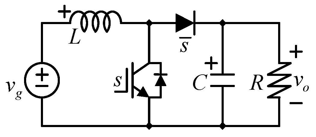
2. The Low Energy Storage Quadratic Boost Converter (LES-QBC)
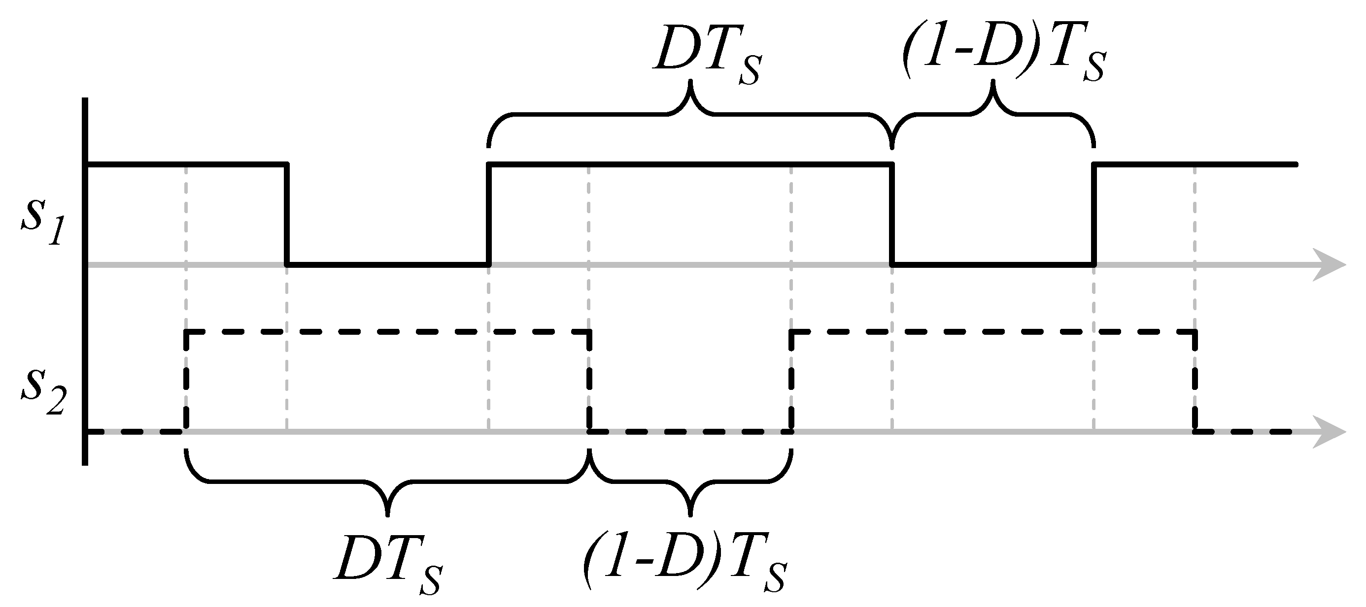
Figure 3 shows the converter understudy (the LES-QBC). It is based on two transistors (s1 and s2), two diodes (s1n and s2n), two capacitors (C1 and C2), and two inductors (L1 and L2).
Each transistor has a complementary diode. s1n is complementary to s1, and s2n is complementary to s2. As in other converters in the literature, in Continuous Conduction Mode (CCM), the complementary diode closes when its transistor is open, and the diode opens when its transistor closes.
In Figure 3, the input voltage source has been called vg. The output voltage has been called vo, and the output current io. In this article, similar to [9], lower case letters are used to represent a full signal (large signal) or their steady state plus variations, upper-case letters are used to represent the steady state or dc value of the signal, and hat letters represent the ac component or variations of the signal around the dc value. Equation (1) is an example of this nomenclature in which x is the full signal composed of
Their dc value and ac variations.
x = X + x ^

The Duty Ratio

The converter’s operation is driven by digital signals that indicate when transistors are open or closed. We call those signals switching functions. The LES-QBC has two transistors and then two switching signals. We can name the switching signals of switching functions as their respective transistors for simplicity and then:
s 1 ( t ) = { 1 s 1 i s c l o s e d 0 s 2 i s o p e n .
s 2 ( t ) = { 1 s 2 i s c l o s e d 0 s 2 i s o p e n .
As in other digital signals, switching signals can be high or low, or they take two values (0 or 1). In practice, switching signals are generated with analog circuits or with microcontrollers (digitally), and the digital one may correspond to 3.3 V or 5 V while the digital cero may correspond to 0 volts.
Transistors are usually switched at a fixed frequency, called switching frequency. This means they open and close depending on the switching signals, but they perform a closing and opening process in a predefined period of fixed time. The converters regulation is performed by adjusting the amount of time switches remain closed. This is called Pulse Width Modulation (PWM), and the switching frequency is indicated as FS. The switching period is defined as the inverse of the switching frequency (TS = 1/FS).
T S = 1 F S .
The duty ratio or duty cycle (d) is the fraction of time a certain transistor is closed divided by the inverse of the switching frequency, also called switching period TS. The duty ratio is equal to the switching function average.
d ( t ) = 1 T S t t + T S s 1 ( τ ) d τ = 1 T S t t + T S s 2 ( τ ) d τ .
If the converter has more than one transistor, each transistor may have a different duty ratio (depending on the topology), in this case, the LES-QBC has two transistors, but its operation considers both of them to have the same duty ratio.

3. Mathematical Model of the LES-QBC

This section discusses the mathematical model of the LES-QBC by using the standard averaging technique. For the sake of simplicity, the model will be derived considering the converter has two cascaded power stages. They will be called input and output power stages. The input power stage is made by L1, C1, s1, and s1n, while the output power stage is made by L2, C2, s2, and s2n.

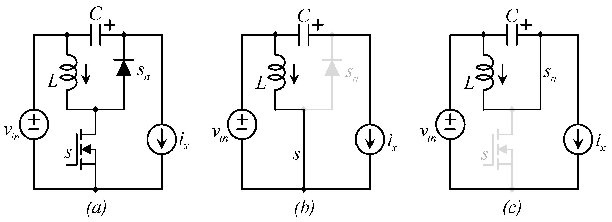
3.1. A Single Power Stage
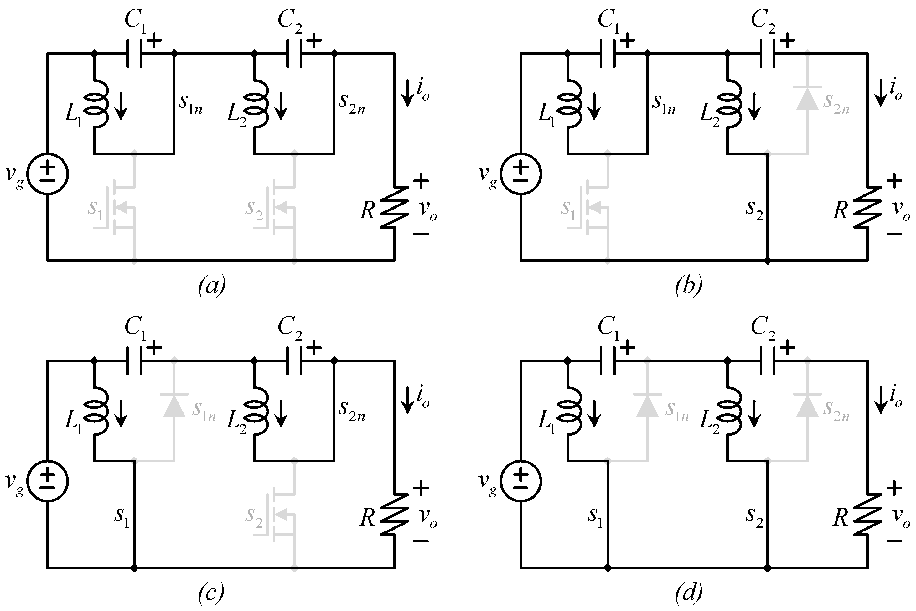
The input and the output power stages have the same topology, and the converter can be seen as a cascaded type of circuit. Figure 4a shows a single power stage. The power stage has two switching states or equivalent circuits. This is considered in the Continuous Conduction Mode (CCM) [9]. Those equivalent circuits are shown in Figure 4b,c. Figure 4b depicts the switching state or equivalent circuit that the converter has if the switch s is closed (while the diode sn is open), and Figure 4c depicts the switching state that the converter has when the transistor is open and the diode is closed.
In Figure 4b, the inductor L is paralleled with the input voltage vin, and then it gets charged. At the same time, the capacitor is getting discharged by the power stage output current ix. This can be written as expressed by Equations (6) and (7).
L d i L d t = v i n .
C d v C d t = i x .
In the other switching state (Figure 4c), the capacitor C and the inductor L are connected in parallel, but in a way in which the inductor discharges and the energy is transferred from the inductor to the capacitor. In other words, the capacitor charges in this state.
The output current (ix) still discharges the capacitor, but the inductor current is larger (as will be shown when studying the equilibrium). The dynamics of the circuit in Figure 4c can be described by the following equations.
L d i L d t = v C .
C d v C d t = i L i x .
By using the standard averaging technique [20], the large-signal or differential equations that describe the dynamics of the circuit in Figure 4a can be written as Equations (10) and (11).
L d i L d t = d ( v i n ) + ( 1 d ) ( v C ) .
C d v C d t = d ( i x ) + ( 1 d ) ( i L i x ) .
Equations (10) and (11) are the large signal model of a single power stage. Those equations can be further simplified to Equations (12)–(13).
L d i L d t = d v i n ( 1 d ) v C .
C d v C d t = ( 1 d ) i L i x .
Equations (12) and (13) describe the behavior of the state variables of the power stage, which are the inductor current and the voltage of the capacitor. They can also be used to find the steady state or equilibrium, which is the operating condition in which state variables no longer vary. This can be found by making the derivatives of state variables equal to zero. The equilibrium of a single power stage can be written as Equations (14) and (15).
V C = D 1 D V i n .
I L = 1 ( 1 D ) I x .
Note that upper case letters are used to indicate that those are the dc components of variables or their equilibrium value.

3.2. The LES-QBC

The LES-QBC is composed of two power stages, such as the one described. The second power stage is the load of the first one; the intermediate voltage Vx and the output voltage Vo can be defined as Equations (16) and (17), respectively.
V x = V g + V C 1 .
V o = V x + V C 2 = V g + V C 1 + V C 2 .
By using Equations (14)–(17), a composed equilibrium can be written for the circuit in Figure 3 as Equations (18)–(23).
V C 1 = D 1 D V g .
V x = 1 1 D V g .
V C 2 = D 1 D V x = D ( 1 D ) 2 V g .
V o = 1 ( 1 D ) 2 V g .
I L 2 = 1 1 D I o .
I L 1 = 1 ( 1 D ) 2 I o .
The voltages Vx and Vo are not state variables, but it is convenient to define them as they are important auxiliary variables. Finally, the gain G, which is the relationship of the voltage at the output port, divided by the voltage at the input port, can be calculated from Equation (21) as Equation (24).
G = 1 ( 1 D ) 2 .

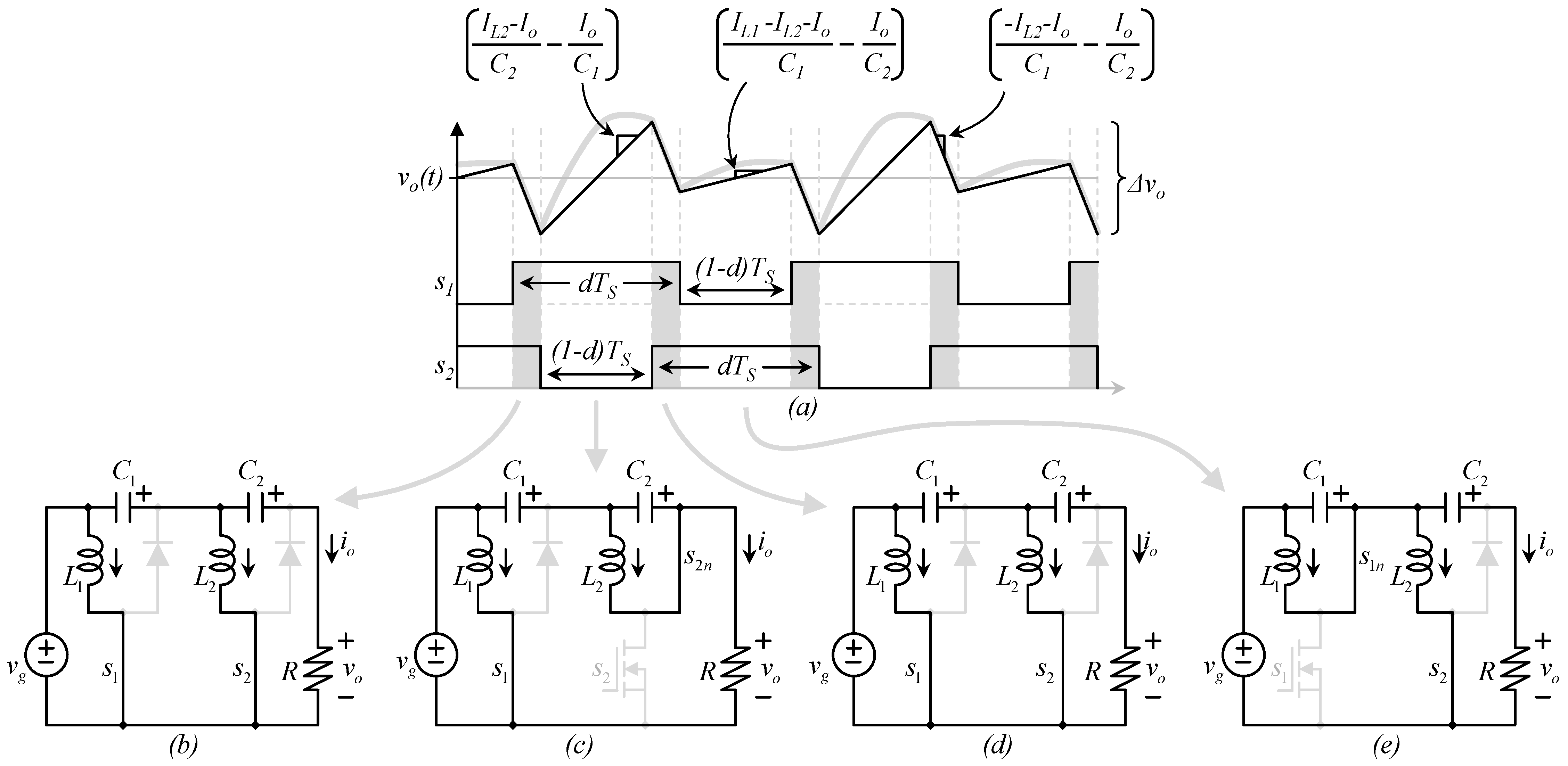
3.3. The Equivalent Circuits of the Real (Composed) Converter

The analysis performed allows us to determine the dc or equilibrium condition of the converter, but the composed or real converter has four possible switching states. This is because the two PWM switching signals are shifted 180° [26,27]. Then, for a particular time instant, the switching signals can obtain four possible combinations. Figure 5 shows two switching functions shifted 180°, such as the one used in the LES-QBC; their duty ratio is greater than 50%; it is actually 66%; we can see that there are three combinations of the instantaneous value of those switching signals: s1 = 1 while s2 = 0, s1 = 1 while s2 = 1, and s1 = 0 while s2 = 1. For duty ratios less than 50%, a fourth state would appear (s1 = 0 and s2 = 0).
A microcontroller may be used to generate those signals and change their duty cycle (their pulse width) symmetrically. This would produce both transistors staying closed for the same average time. Figure 6 shows the four possible switching states of the LES-QBC.
Despite the four possible states, only three of them appear in a certain operation [26,27] (and only two if D = 0.5). If the duty ratio surpasses 0.5, the states that appear are {0, 1}, {1, 0}, and {1, 1}, (see Figure 5), when the duty ratio is lower than 0.5, the states that appear are {0, 1}, {1, 0}, and {0, 0}, and when the duty cycle is exactly 0.5, the switching states that appear are only {0, 1} and {1, 0}.

3.4. Calculating the Voltage Ripple at the Output Port

Considering the real equivalent circuits in Figure 6 is important since the output voltage ripple (OVR) is calculated based on those circuits. The OVR is related to the power quality at the output port of the converter. Ideally, the voltage at the output port is expected to look like a perfect constant value with no ripple (or variation), but the ripple is produced by the transistors switching and then, it is unavoidable in most cases. A large value of capacitance in capacitors would reduce the ripple, but this would result in large-size capacitors, which is unwanted. This compromise between the voltage ripple and the size of capacitors is well known in the field of power electronics since it happens in most of the topologies, which is why the objective is to minimize the OVR without increasing the capacitor’s stored energy.
In a traditional converter, like in the standard boost converter, there are two equivalent circuits or switching states, and the OVR can be calculated by analyzing one of them. In this case, the converter has four switching stages, and we must evaluate two of them to know the maximum voltage change.
In the LES-QBC, during the operation, there are four different times when the output voltage changes differently; for example, Figure 7a shows a zoom in the output voltage ripple for the operation in which D = 0.6, along with the firing signals for s1, and s2. The four times correspond to a sequence in which the set {s1, s2} is equal to {1, 1}, {1, 0}, {1, 1}, and {0, 1} (and repeat). The switching states are repeated in Figure 7 to see the sequence clearly. Figure 7b shows the state {s1, s2} = {1, 1}, Figure 7c shows the state {s1, s2} = {1, 0}, Figure 7d shows the state {s1, s2} = {1, 1}, and Figure 7e shows the state {s1, s2} = {0, 1}. Figure 7a also indicates the slopes of the output voltage, which can also be derived from the equivalent circuits.
The decreasing state, the state in which the output voltage is decreasing, has the same equivalent circuit and equation at both times in the sequence. The output voltage ripple can be evaluated in all four states, but since the decreasing states are equal, the difference may be in the increasing states.
Depending on the parameters (for example, the capacitance on capacitors), one increasing state may be larger than the second and vice versa; if the increasing states are equal, then they are also equal to the decreasing states, and then evaluating any of the four times provide the same value.
Then, the output voltage ripple can be calculated by evaluating both increasing states and determining which is the largest. Those increasing states are shown in Figure 7 or in Figure 6b, which corresponds to Equation (25), and Figure 6c, which corresponds to Equation (26). They are called Δvo1 and Δvo2, respectively.
Δ v o 1 = ( 1 D ) T S 2 ( I L 1 I L 2 I o C 1 I o C 2 ) .
Δ v o 2 = ( 1 D ) T S 2 ( I o C 1 + I L 2 I o C 2 ) .
Figure 7 also shows an approximation of the classical deviation from the ideal waveforms caused by the inductor currents’ trapezoidal waveform. For example, the experimental waveform would look like the theoretical if inductor currents were perfectly rectangular. However, since inductors are getting charged or discharged and seem like a triangular waveform, the output voltage looks like this softened shape.
We can substitute Equations (22) and (23) in Equations (25) and (26) to obtain the equations in terms of Io; furthermore, we can express C1 and C2 in terms of a single capacitance C and a ratio parameter β, to have a single capacitance and their relationship like Equation (27).
C 1 = C ,   C 2 = β C .
Those substitutions lead to Equations (28) and (29).
Δ v o 1 = T S I o 2 C ( ( 1 + β ) D 2 + ( 3 β + 2 ) D ( β + 1 ) ( 1 D ) β ) .
Δ v o 2 = I o T S 2 C ( D ( 1 + β ) β β ) .
The optimizer’s goal is to minimize the maximum ripple; in other words, the maximum value is calculated from Equations (25) or (26).

4. The Particle Swarm Optimization (PSO) Algorithm

The PSO is a popular metaheuristic optimization algorithm that has been widely applied to various scientific and engineering problems. It is inspired by the social behavior of bird flocks and fish schools, where each individual (particle) in the group follows a simple set of rules to search for the optimal solution. PSO has been shown to be effective in solving complex optimization problems in various fields such as engineering, economics, and computer science. This iterative method has shown robustness in avoiding local solutions, in a search space. This kind of method allows us to find potential solutions in an iterative generation process and evolve them with the purpose of finding the “best solution” in a reasonable period of time.
Metaheuristic algorithms can be classified into classical and evolutionary methods [31]. The first of them calculates the function gradient to approximate the minimum or maximum of the function, but this kind of procedure is not applicable for several cases, their applicability depends on the objective function which needs to be unimodal and differentiable. On the other hand, evolutionary methods do not use the gradient function, they are inspired by natural processes. The PSO algorithm is a simple, effective and proven method to optimize and has been previously used in the field of power electronics.

4.1. Particle Swarm Optimization

Initially introduced by Kennedy and Eberhart in 1995 [32], the PSO algorithm is inspired by the social behavior of bird flocks or fish schools. In PSO, a population of particles, which represent candidate solutions, moves through the search space to find the optimal solution.
Each particle has a position and a velocity, and it updates its position and velocity in each iteration based on its own best position found so far and the best position found by the swarm. The PSO algorithm is effective in a wide range of optimization problems, including function optimization, parameter tuning, feature selection, and clustering.

4.2. Initialization

The first step is to initialize the population, which is a set of particles with a particular position and velocity; this is usually performed randomly to have a dispersed set over the search space, and pre-defined bounds limit the position. After that, each solution is substituted in the objective function in order to determine which of the solutions is the best (at least at this moment, it is an iterative procedure). Local and global particles are detected. Then, an iterative process starts, where the velocity and position are updated and applied to each solution.

4.3. Update Velocity

Velocity plays an important role in the process. IT is updated after each iteration based on the global and best local solutions obtained in each iteration. The process uses cognitive and social factors. The velocity v i k of each particle x i k is updated by using Equation (30).
v i k + 1 = v i k + c 1 ( r 1 k ( p i k x i k ) ) + c 2 ( r 2 k ( g k x i k ) ) .
where k represents the current iteration, v i k + 1 is the updated velocity for the following generation (k + 1), of the particle x i k , v i k is the current velocity, p i k is the local best so far of x i k , g k is the global best so far. Additionally, r 1 k and r 2 k are random values in the interval of [0, 1], while the parameters c1, and c2 are the cognitive and social factors, respectively.

4.4. New Particle Generation

New particles are generated based on the previous particles and their speed; this is achieved with Equation (31).
x i k + 1 = x i k + v i k + 1 .
where x i k + 1 is the position of the new particle; generated for each particle x i k , each iteration substitutes the old particle with a new one according to the particle’s velocity v i k + 1 .
This process is called particle’s update. The process of updating solutions is held for a predefined number of iterations.
The PSO algorithm has several advantages that make it a popular optimization method, including (i) Simplicity: The PSO algorithm is easy to implement and understand and it has only a few parameters to tune; (ii) Global optimization: PSO is a population-based algorithm, which means that it can explore multiple regions of the search space in parallel. This allows the algorithm to avoid getting stuck in local optima and can find the global optimum or near-global optimum; (iii) Convergence speed: PSO typically converges faster than other optimization algorithms, especially in high-dimensional search spaces; (iv) Robustness: PSO is less sensitive to the initial population than other optimization algorithms and can handle noisy or stochastic objective functions; (v) Scalability: PSO can be parallelized easily, which makes it suitable for large-scale optimization problems; (vi) Versatility: PSO can be adapted to a wide range of optimization problems, including continuous, discrete, and mixed-variable optimization, as well as constrained and unconstrained optimization.
Overall, the PSO algorithm is a powerful and versatile optimization method that can be applied to many different problems. Its simplicity, global optimization capability, and fast convergence make it a popular choice for researchers and practitioners alike.

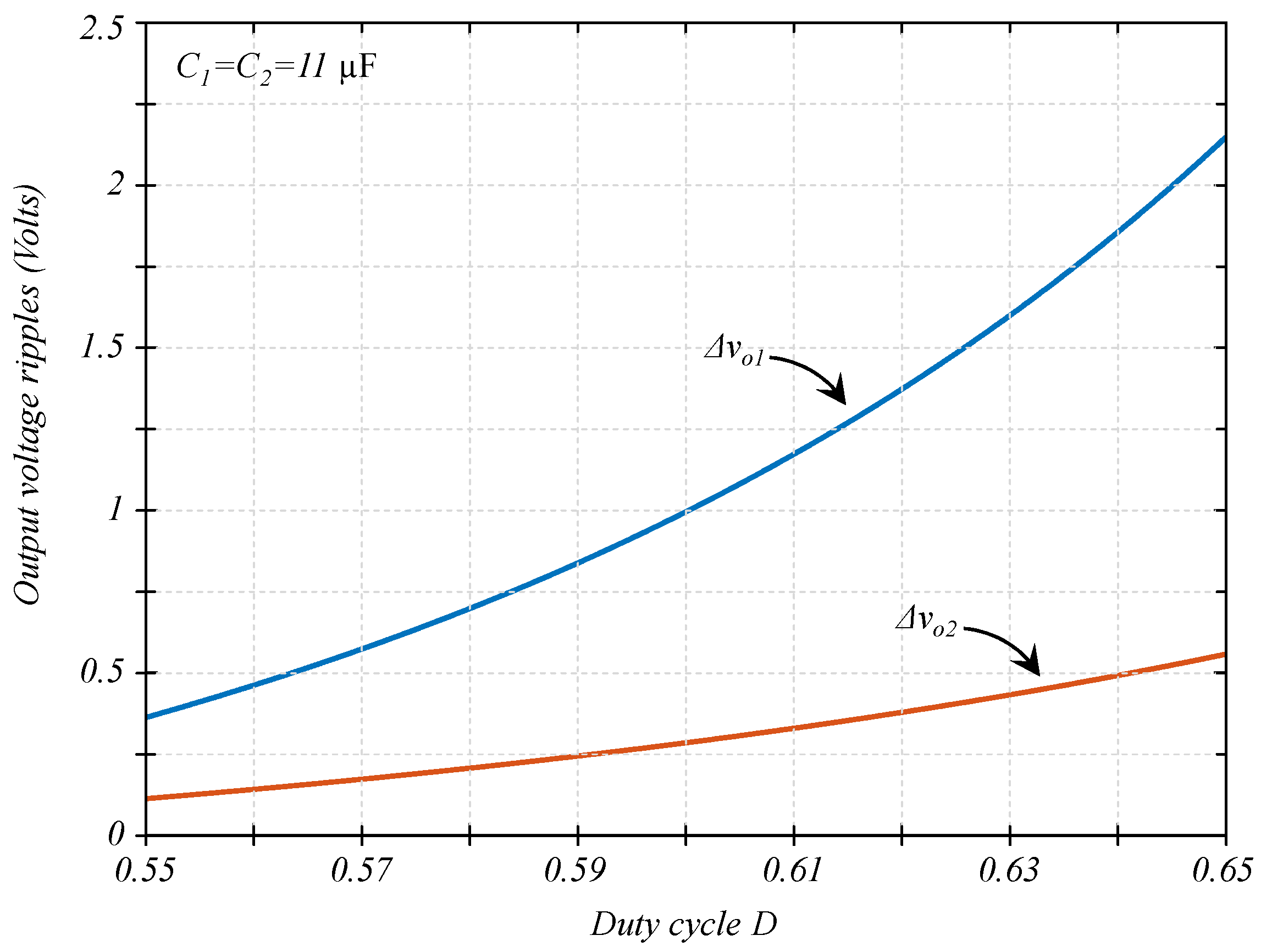
5. Numerical Example

Let us introduce a numerical example to corroborate the optimization’s effectiveness. The exercise consists of designing an LES-QBC, particularly selecting the capacitors. The considered inductors are L1 = 250 µH and L2 = 250 µH; the converter switching frequency was chosen as FS = 20 kHz. The output voltage is desired to be 120 V with an input of around 20 V. The load is resistive Ro = 200 Ω. The duty ratio of the converter operates between 0.55 to 0.65.
The optimization’s starting point considers both capacitors equal C1 = C2 = 11 µF. The experimental results in [26,27] were provided with a different value but also with equal capacitors. When evaluating the Output Voltage Ripple (OVR) with Equations (25) and (26), the OVR in the range of duty cycle previously described, the OVR seems like in Figure 8.
We can conclude from Figure 8 that the maximum OVR is around 2.3 V, achieved at the operating point in which D = 0.65. We can also say the OVR is dominated by Δvo1 Equation (25), which is larger in this example than Δvo2 Equation (26) in the full range, but we must evaluate both equations since other combinations of parameters may lead to different behavior. For example, if C1 = 22 µF and C2 = 11 µF, the result would be different. Figure 9 shows the capacitor’s stored energy for the described example.
The capacitor’s stored energy (Figure 9) was calculated as Equation (32).
J 1 = C 1 ( V C 1 ) 2 2 + C 2 ( V C 2 ) 2 2 .
We can see from Figure 9, the stored energy depends on the operating condition, the maximum stored energy is around 70 mJ, and it is also achieved at the operating point in which D = 0.65.

The Problem from the Optimization Point of View

The optimization problem consists of minimizing the output voltage ripple given by the largest value obtained from Equations (25) or (26), the main constraint is not to increase the capacitor’s stored energy Equation (34), the solution to the problem must be a pair of parameters (C1 and C2) but with the derivation of Equations (28) and (29), if it can be focused on one variable (β), which can be used to calculate the capacitance of capacitors C1 and with Equation (27). The solution may have decimals in the capacitance values, and the solution may be non-commercial values, but they can give us an idea of the commercial values, and we can then evaluate the OVR and the stored energy to ensure the OVR is smaller than the non-optimized solution, and the stored energy is not surpassing the one in the non-optimized solution.
The stored energy was chosen as 70 mJ since this is near the maximum stored energy of the non-optimized solution. The problem can be formulated as the following.
min β f ( β ) = { Δ v o 1 = ( ( 1 + β ) D 2 + ( 3 β + 2 ) D ( β + 1 ) ( 1 D ) β ) , i f ( Δ v o 1 > Δ v o 2 ) Δ v o 2 = ( D ( 1 + β ) β β ) o t h e r w i s e .
Subject to:
C ( V C 1 ) 2 2 + β C ( V C 2 ) 2 2 < = J 1 .
0 C 2 J 1 ( V C 1 ) 2 .
0 β C 2 J 1 ( V C 2 ) 2 .
The parameters of this problem are the Maximum Stored Energy J1 = 70 mJ, when the Duty cycle D = 0.65. Since the optimization is performed by a single duty cycle, it is advised to use the maximum duty cycle in which the converter will operate, since the maximum duty cycle corresponds to the maximum output voltage ripple.

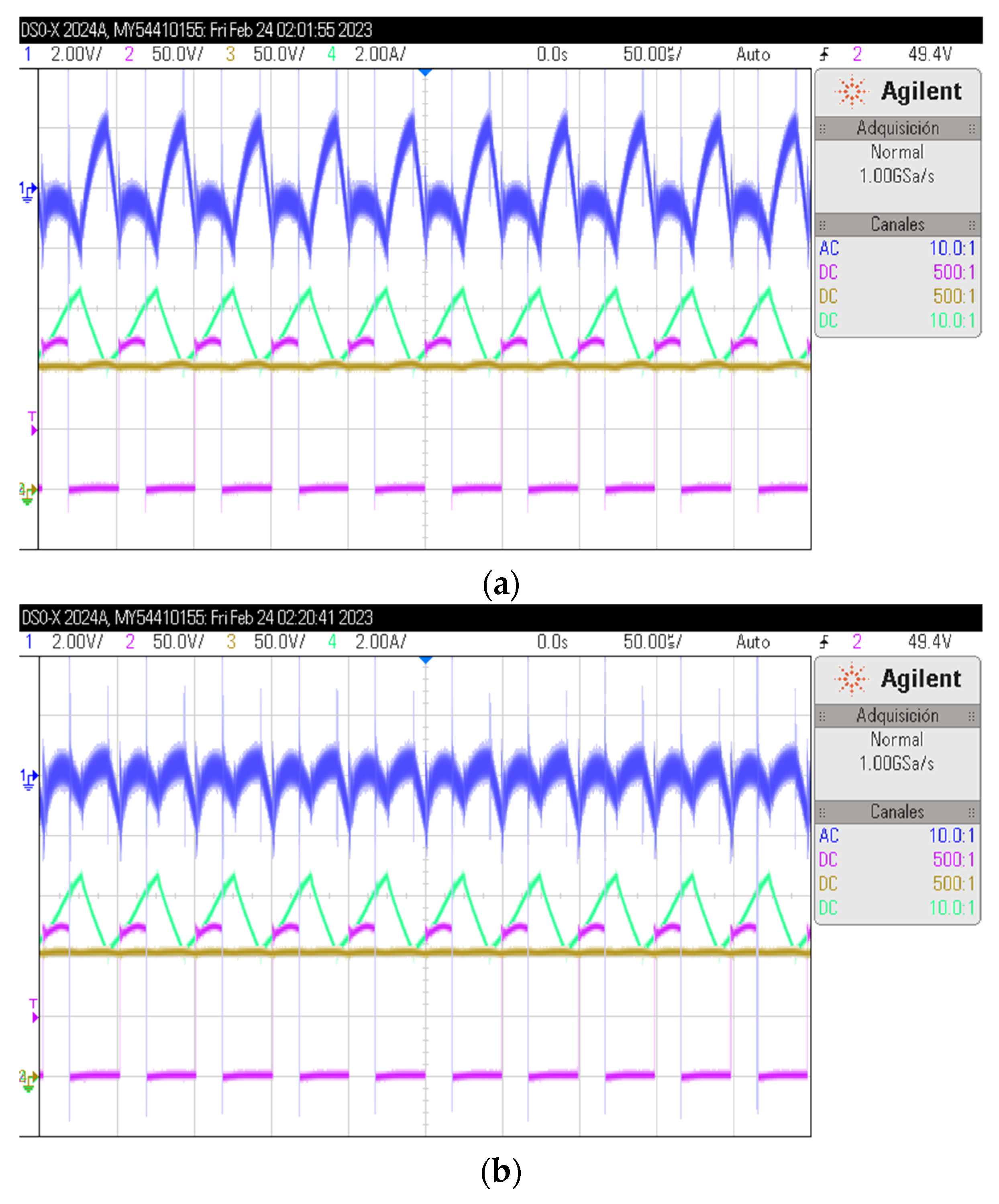
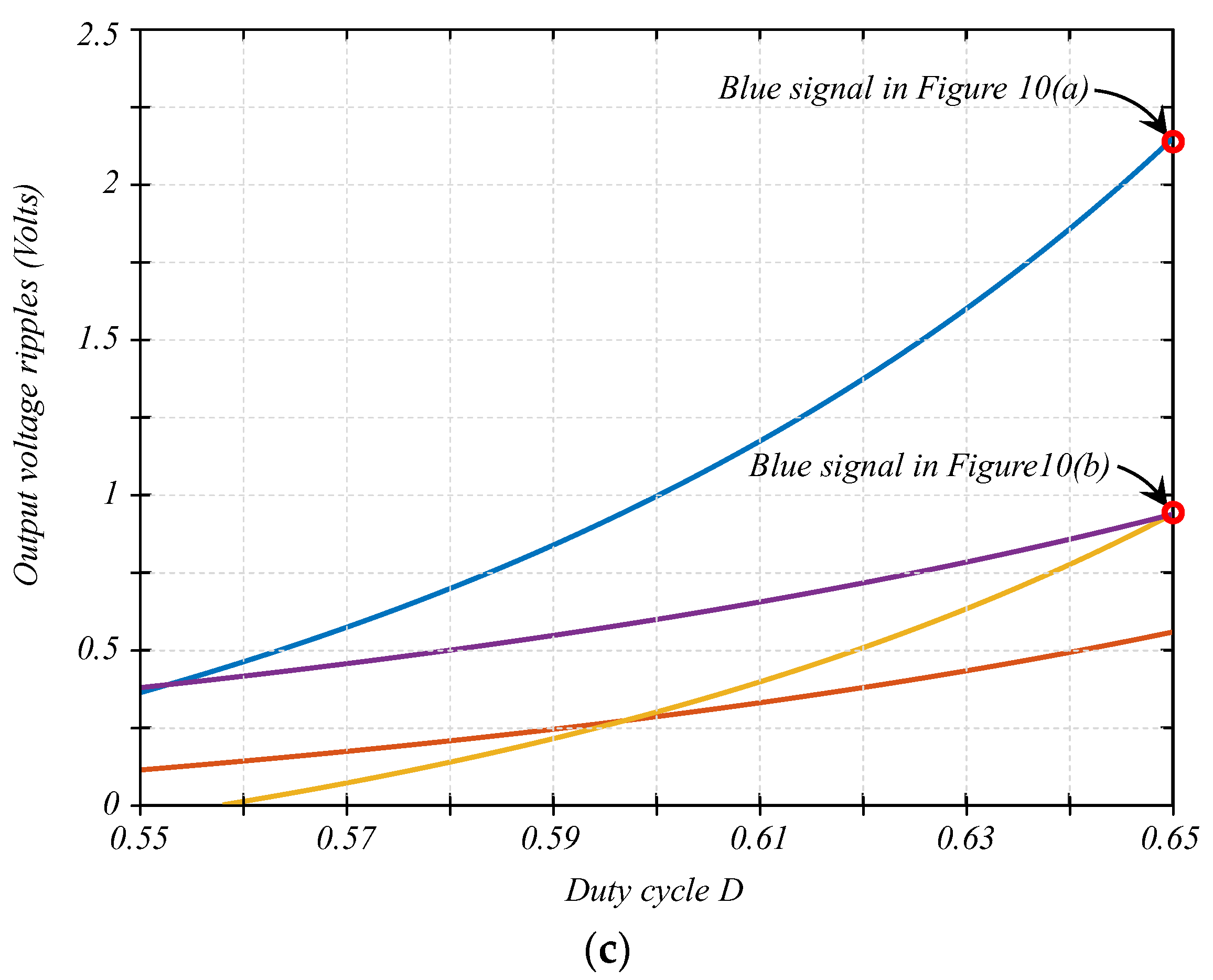
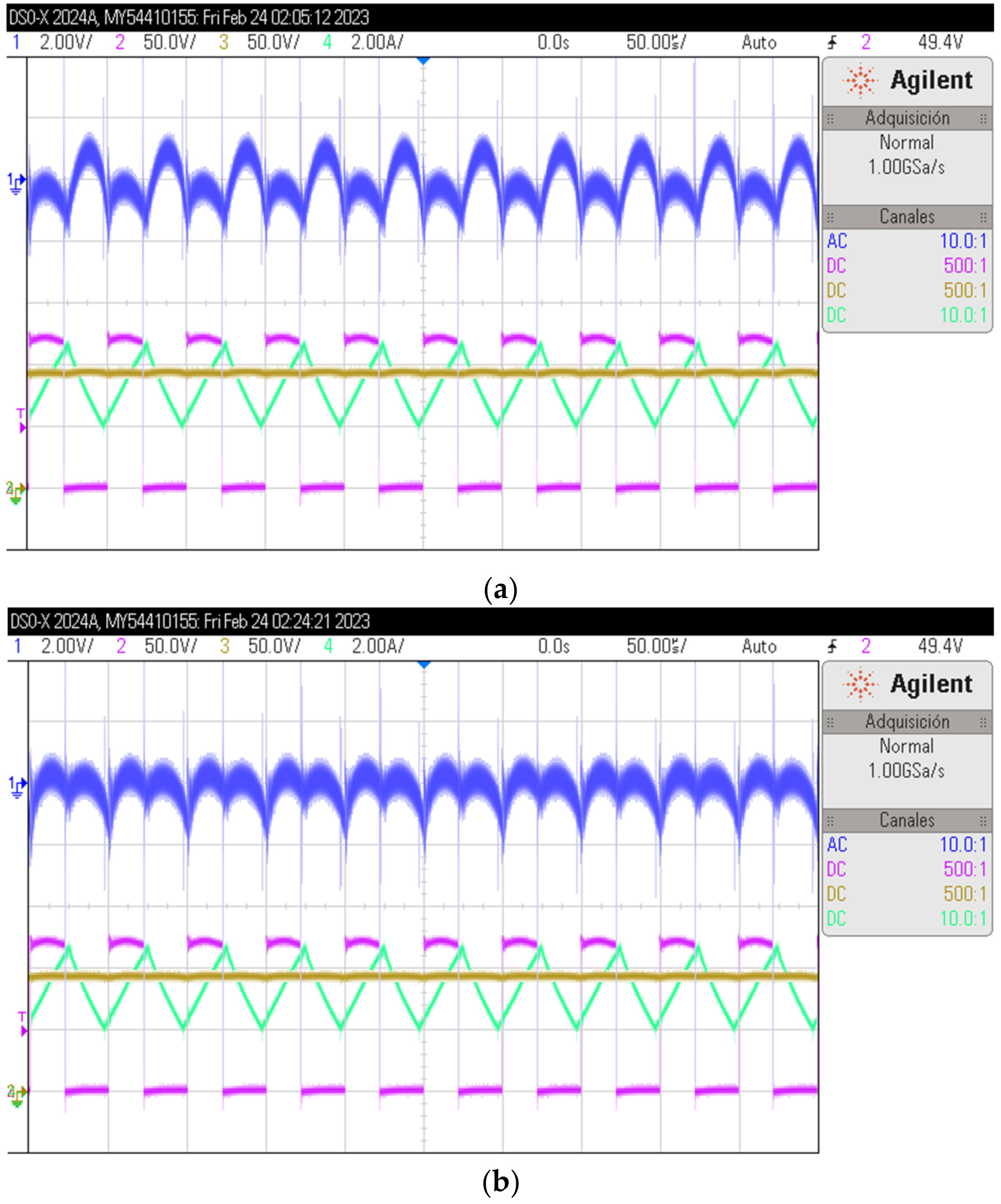
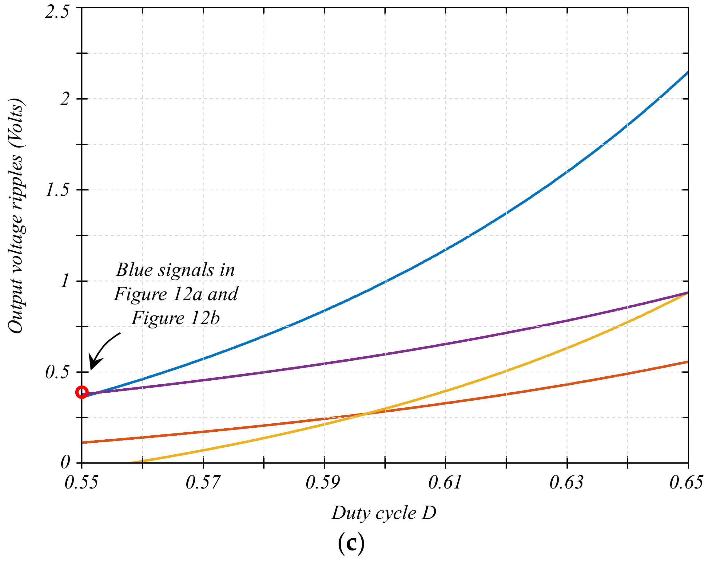
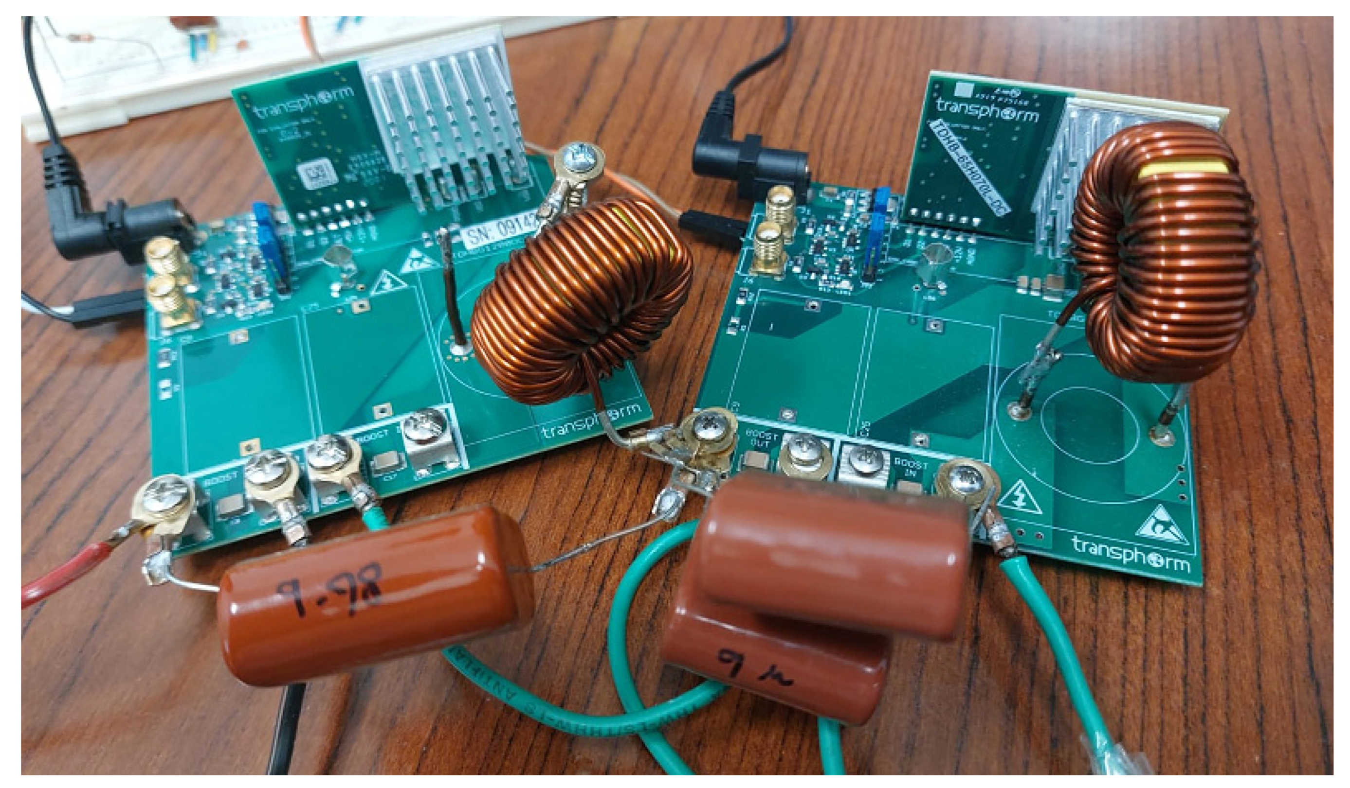
6. The Solution and Experimental Results

The discussed problem solution is C1 = 18.68 µF and C2 = 10.290 µF, those are non-commercial values, we perform experiments with commercial values of C1 = C2 = 11 µF for the non-optimized experiment and C1 = 19 µF and C2 = 10 µF, for the optimized version. Three operating points were analyzed, when D = {0.65, 0.60, 0.55}.
Figure 10 shows important waveforms of the converter operation when D = 0.65. Figure 10a shows the non-optimized design. From top to bottom, we can see the main signal in Figure 10 is the zoom in the measurement of vC1 + vC2 at 2 V/div (measured with ac coupling). In green, we can see the current through the inductor L1 at 2 A/div; in pink, we can see the voltage across the transistor s2 at 50 V/div. Their peak voltage is equal to the output voltage; in gold color, we can see the measurement of vC1 + vC2 at 50 V/div (with dc coupling).
In Figure 10b, we can see the same signals but for the optimized design. Evidently, the output voltage ripple is smaller. In Figure 10c, we can see the graphs of the output voltage ripple similar to Figure 8. The blue and orange signals are parameters for the non-optimized design, while the purple and yellow lines are for the optimized design.
Figure 11 shows the same signals as Figure 10, except for the case when D = 0.6.
Figure 12 shows the same signals as Figure 10 and Figure 11, except for the case when D = 0.55.
We can observe that when the duty cycle is reduced, the difference between the amplitude of the output voltage ripple is smaller (from the non-optimized to the optimized), which can also be observed in Figure 10c. Figure 12 shows that the output voltage ripple from both situations is almost the same. Still, the optimized design shows an average reduction in the output voltage ripple in the full operating condition. Finally, Figure 13 shows a photo of the experimental prototype.

7. Conclusions

This article explores the optimal selection of capacitors for a recently introduced dc-dc converter topology. The converter under study is the so-called Low Energy Storage Quadratic Boost Converter (LES-QBC), a quadratic type of converter that requires capacitors to be rated to a smaller voltage compared to the traditional quadratic boost converter.
This work formulates an optimization problem in which the selection of capacitors can be used to minimize the output voltage ripple. A design example was performed with the LES-QBC with equal capacitors (non-optimized) and the proposed optimal design; both converters had the same stored energy in capacitors, and the optimization was performed by using the Particle Swarm Optimization (PSO) algorithm. The study was performed numerically and demonstrated by experimental results. The results showed that the optimized design has a smaller output voltage ripple in the defined operation range; in the maximum duty cycle (D = 0.65), the reduction in output voltage ripple was observed to be around 50%. The experimental results were in good agreement with the theoretical expectations.

Author Contributions

J.C.R.-C. and J.E.V.-R. contributed to the conceptualization of the article; A.A.-R. contributed to the optimization methodology; J.S.-R. contributed to the software and validation, A.A.-R. and J.E.V.-R. contributed to the formal analysis; and J.C.R.-C. wrote the draft and manuscript preparation. All authors have read and agreed to the published version of the manuscript.

Funding

The authors would like to thank Universidad Panamericana, for their support through the program “Fomento a la Investigación UP 2022”, and project “Estudio de algoritmos heurísticos y metaheurísticos en la optimización de problemas en la ingeniería” UP-CI-2022-GDL-02-ING. And to the Universidad Panamericana Dirección Institucional de Investigación.

Data Availability Statement

Not applicable.

Conflicts of Interest

The authors declare no conflict of interest.

References

  1. Rashid, M. Power Electronics: Circuits, Devices and Applications, 3rd ed.; Prentice Hall: London, UK, 2004; p. 762. [Google Scholar]
  2. Undeland, M.N.; Robbins, W.P.; Mohan, N. Power Electronics in Converters, Applications, and Design, 3rd ed.; John Whiley & Sons: Hoboken, NJ, USA, 1995; p. 763. [Google Scholar]
  3. Khan, S.; Rahman, K.; Tariq, M.; Hameed, S.; Alamri, B.; Babu, T.S. Solid-State Transformers: Fundamentals, Topologies, Applications, and Future Challenges. Sustainability 2022, 14, 319. [Google Scholar] [CrossRef]
  4. Narayanaswamy, J.; Mandava, S. Non-Isolated Multiport Converter for Renewable Energy Sources: A Comprehensive Review. Energies 2023, 16, 1834. [Google Scholar] [CrossRef]
  5. Saadaoui, A.; Ouassaid, M.; Maaroufi, M. Overview of Integration of Power Electronic Topologies and Advanced Control Techniques of Ultra-Fast EV Charging Stations in Standalone Microgrids. Energies 2023, 16, 1031. [Google Scholar] [CrossRef]
  6. Rafiq, U.; Murtaza, A.F.; Sher, H.A.; Gandini, D. Design and Analysis of a Novel High-Gain DC-DC Boost Converter with Low Component Count. Electronics 2021, 10, 1761. [Google Scholar] [CrossRef]
  7. Mohammadzadeh Shahir, F.; Gheisarnejad, M.; Khooban, M.-H. A New Transformer-Less Structure for a Boost DC-DC Converter with Suitable Voltage Stress. Automation 2021, 2, 220–237. [Google Scholar] [CrossRef]
  8. de Carvalho, M.R.S.; Neto, R.C.; Barbosa, E.J.; Limongi, L.R.; Bradaschia, F.; Cavalcanti, M.C. An Overview of Voltage Boosting Techniques and Step-Up DC-DC Converters Topologies for PV Applications. Energies 2021, 14, 8230. [Google Scholar] [CrossRef]
  9. Erickson, R.W.; Maksimovic, D. Fundamentals of Power Electronics; Springer: New York, NY, USA, 2001. [Google Scholar]
  10. Lenk, R. Practical Design of Power Supplies; Institute of Electrical and Electronics Engineers (IEEE): Piscataway, NJ, USA; Wiley: Hoboken, NJ, USA, 2005. [Google Scholar]
  11. Rosas-Caro, J.C.; Ramirez, J.M.; Peng, F.Z.; Valderrabano, A. A DC-DC multilevel boost converter. IET Power Electron. 2010, 3, 129–137. [Google Scholar] [CrossRef]
  12. Rosas-Caro, J.C.; Mayo-Maldonado, J.C.; Valdez-Resendiz, J.E.; Alejo-Reyes, A.; Beltran-Carbajal, F.; López-Santos, O. An Overview of Non-Isolated Hybrid Switched-Capacitor Step-Up DC–DC Converters. Appl. Sci. 2022, 12, 8554. [Google Scholar] [CrossRef]
  13. Haider, Z.; Ulasyar, A.; Khattak, A.; Zad, H.S.; Mohammad, A.; Alahmadi, A.A.; Ullah, N. Development and Analysis of a Novel High-Gain CUK Converter Using Voltage-Multiplier Units. Electronics 2022, 11, 2766. [Google Scholar] [CrossRef]
  14. Zaid, M.; Malick, I.H.; Ashraf, I.; Tariq, M.; Alamri, B.; Rodrigues, E.M.G. A Nonisolated Transformerless High-Gain DC–DC Converter for Renewable Energy Applications. Electronics 2022, 11, 2014. [Google Scholar] [CrossRef]
  15. Jana, A.S.; Lin, C.-H.; Kao, T.-H.; Chang, C.-H. A High Gain Modified Quadratic Boost DC-DC Converter with Voltage Stress Half of Output Voltage. Appl. Sci. 2022, 12, 4914. [Google Scholar] [CrossRef]
  16. Zaid, M.; Lin, C.-H.; Khan, S.; Ahmad, J.; Tariq, M.; Mahmood, A.; Sarwar, A.; Alamri, B.; Alahmadi, A. A Family of Transformerless Quadratic Boost High Gain DC-DC Converters. Energies 2021, 14, 4372. [Google Scholar] [CrossRef]
  17. Loera-Palomo, R.; Morales-Saldaña, J.A.; Rivero, M.; Álvarez-Macías, C.; Hernández-Jacobo, C.A. Noncascading Quadratic Buck-Boost Converter for Photovoltaic Applications. Micromachines 2021, 12, 984. [Google Scholar] [CrossRef] [PubMed]
  18. Bhavani, S.; Sivaprakasam, A. Dual Mode Symmetrical Proportional Resonant Controlled Quadratic Boost Converter for PMSM-Drive. Symmetry 2023, 15, 147. [Google Scholar] [CrossRef]
  19. Luo, F.L.; Ye, H. Positive output cascade boost converters. IEE Proc. Electr. Power Appl. 2004, 151, 590–606. [Google Scholar] [CrossRef]
  20. Ortiz-Lopez, M.G.; Leyva-Ramos, J.; Carbajal-Gutierrez, E.E.; Morales-Saldaña, J.A. Modelling and analysis of switch-mode cascade converters with a single active switch. IET Power Electron. 2008, 1, 478–487. [Google Scholar] [CrossRef]
  21. Leyva-Ramos, J.; Lopez-cruz, J.M.; Ortiz-lopez, M.G.; Diaz-Saldierna, L.H. Switching regulator using a high step-up voltage converter for fuel-cell modules. IET Power Electron. 2013, 6, 1626–1633. [Google Scholar] [CrossRef]
  22. Lopez-Santos, O.; Martinez-Salamero, L.; Garcia, G.; Valderrama-Blavi, H.; Sierra-Polanco, T. Robust sliding mode control design for a voltage-regulated quadratic boost converter. IEEE Trans. Power Electron. 2015, 30, 2313–2327. [Google Scholar] [CrossRef]
  23. Jiang, W.; Chincholkar, S.H.; Chan, C. Modified voltage-mode controller for the quadratic boost converter with improved output performance. IET Power Electron. 2018, 11, 2222–2231. [Google Scholar] [CrossRef]
  24. Ye, Y.M.; Cheng, K.W.E. Quadratic boost converter with low buffer capacitor stress. IET Power Electron. 2014, 7, 1162–1170. [Google Scholar] [CrossRef]
  25. Loera-Palomo, R.; Morales-Saldaña, J.A. Family of quadratic step-up dc–dc converters based on non-cascading structures. IET Power Electron. 2015, 8, 793–801. [Google Scholar] [CrossRef]
  26. Lopez-Santos, O.; Mayo-Maldonado, J.C.; Rosas-Caro, J.C.; Valdez-Resendiz, J.E.; Zambrano-Prada, D.A.; Ruiz-Martinez, O.F. Quadratic boost converter with low-output voltage ripple. IET Power Electron. 2020, 13, 1605–1612. [Google Scholar] [CrossRef]
  27. López-Santos, O.; Varón, N.L.; Rosas-Caro, J.C.; Mayo-Maldonado, J.C.; Valdez-Reséndiz, J.E. Detailed Modeling of the Low Energy Storage Quadratic Boost Converter. IEEE Trans. Power Electron. 2022, 37, 1885–1904. [Google Scholar]
  28. Ponniran, A.; Orikawa, K.; Itoh, J.-I. Minimum flying capacitor for N-level capacitor DC/DC boost converter. In Proceedings of the 9th International Conference on Power Electronics and ECCE Asia (ICPE-ECCE Asia), Seoul, Korea, 1–5 June 2015; pp. 1289–1296. [Google Scholar] [CrossRef]
  29. Drofenik, U.; Laimer, G.; Kolar, J.W. Theoretical converter power density limits for forced convection cooling. In Proceedings of the International Conference Power Electronics, Intelligent Motion, Power Quality, Nurnberg, Germany, 7–9 June 2005. [Google Scholar]
  30. Obara, H.; Sato, Y. Selection criteria of capacitors for flying capacitor converters. IEEJ J. Ind. Appl. 2015, 4, 105–106. [Google Scholar] [CrossRef]
  31. Yang, X.-S. Engineering Optimization; John Wiley and Sons: Hoboken, NJ, USA, 2010. [Google Scholar]
  32. Eberhart, R.; Kennedy, J. A new optimizer using particle swarm theory. In Proceedings of the Sixth International Symposium on Micro Machine and Human Science, Nagoya, Japan, 4–6 October 1995; pp. 39–43. [Google Scholar]
Figure 1. The traditional boost converter.
Energies 16 02510 g001
Figure 2. (a) The traditional quadratic boost converter; (b) quadratic boost studied in [24,25].
Energies 16 02510 g002
Figure 3. The LES-QBC topology.
Energies 16 02510 g003
Figure 4. A single circuit stage (a) topology, (b) switching state of the converter when the switch is closed, (c) switching state of the converter when the switch is open.
Energies 16 02510 g004
Figure 5. Switching functions of the LES-QBC and their relation with the duty cycle D.
Energies 16 02510 g005
Figure 6. Switching states of the converter with two switching functions: (a) {s1, s2} = {0, 0}; (b) {s1, s2} = {0, 1}; (c) {s1, s2} = {1, 0}; and (d) {s1, s2} = {1, 1}.
Energies 16 02510 g006
Figure 7. OVR description (a) zoom in the OVR, times and slopes, (b) state {1,1}, (c) state {1,0}, (d) state {1,1}, (e) state {0,1}.
Energies 16 02510 g007
Figure 8. OVR in the described operation range (duty ratio from 0.55 to 0.65) with C1 = C2 = 11 µF.
Energies 16 02510 g008
Figure 9. Capacitors stored-energy in the described example in which C1 = C2 = 11 µF.
Energies 16 02510 g009
Figure 10. Results when D = 0.65: (a) signals in the non-optimized design: output voltage ripple (blue), iL1 (green), voltage across s2, voltage vC1 + vC2; (b) signals in the optimized design (same description as (a)); (c) calculated output voltage ripples.
Energies 16 02510 g010aEnergies 16 02510 g010b
Figure 11. Results when D = 0.60: (a) signals in the non-optimized design: output voltage ripple (blue), iL1 (green), voltage across s2, voltage vC1 + vC2; (b) signals in the optimized design (same description as (a)), (c) calculated output voltage ripples.
Energies 16 02510 g011aEnergies 16 02510 g011b
Figure 12. Results when D = 0.55: (a) signals in the non-optimized design: output voltage ripple (blue), iL1 (green), voltage across s2, voltage vC1 + vC2; (b) signals in the optimized design (same description as (a)), (c) calculated output voltage ripples.
Energies 16 02510 g012aEnergies 16 02510 g012b
Figure 13. Experimental prototype.
Energies 16 02510 g013
Disclaimer/Publisher’s Note: The statements, opinions and data contained in all publications are solely those of the individual author(s) and contributor(s) and not of MDPI and/or the editor(s). MDPI and/or the editor(s) disclaim responsibility for any injury to people or property resulting from any ideas, methods, instructions or products referred to in the content.

