Abstract
This work presents a design for uninterruptible power supply inverters using Pareto front optimization for improved cost and efficiency. Three PWM modulation techniques applied to the full-bridge inverter are analyzed. As a result, the best MOSFET design solution in terms of the cost and efficiency of the inverter is evaluated based on a database with 47 power MOSFETs. Using the Pareto front, the optimal and sub-optimal solutions are compared, considering the three modulation techniques and the characteristics of MOSFETs manufactured for different voltage levels. Thermal and electrical measurements are used to validate the models.
1. Introduction
Uninterruptible power supplies (UPSs) are electronic systems capable of supplying high quality power to critical loads [1,2,3,4,5,6,7]. These are used for a wide range of applications, from systems rated at less than 1 kVA (single phase), to systems rated at more than 1000 kVA (three phase). High-power UPSs are used as temporary backup sources for large equipment and data centers, supplied by battery banks with hundreds of volts [8,9,10]. Lower-power UPSs are used in small office or home office (SOHO) applications, including converters that generally operate on battery voltages equal to or below 24 V, and are mainly classified as offline or line-interactive type [8,9,11].
In SOHO UPSs, the batteries can be connected to the load using a full-bridge converter. It is often necessary to raise the output voltage of the inverter to the AC output voltage using a low frequency transformer [8,9,11,12]. These topologies are known as ferroresonant-based UPSs [13,14,15,16]. Due to the use of the step-up transformer, the current drawn from the batteries and flowing through the inverter is higher than the load current, which causes high current stress on the inverter [12].
In order to lower harmonic distortions caused by converter switching, three-level modulations are employed [17,18,19,20]. Three modulation techniques are frequently utilized in the full bridge converter [11,17,20]:
- Discontinuous modulation (DM): the converter legs alternate switching within a carrier period. One converter leg is switched at high frequency during half of the fundamental (50 or 60 Hz) cycle, and the other converter leg is switched in the remaining half of the cycle [17] (Figure 1a);
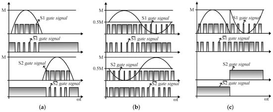 Figure 1. Three-level modulations applied to single-phase full-bridge inverter. (a) DM. (b) PS. (c) DSPLS.
 - Phase-shifted modulation (PS): both converter legs switch at high frequency [17] (Figure 1b);
- Discontinuous single-phase leg switched modulation (DSPLS): one converter leg switches at high frequency, while the other switches at the rate of the fundamental cycle [17] (Figure 1c).
Different modulation techniques will have different influences on the voltage and current of the semiconductors, which affects losses directly. To reduce losses and improve efficiency, optimization techniques are used [21,22,23,24,25,26]. In low-voltage full-bridge applications, converter optimization faces the challenge of selecting the part number of the MOSFETs of the inverter, considering their relation to efficiency and cost. These two metrics are often conflicting, and the Pareto front optimization is used as a tool to determine the compromise among them. Limits of the Pareto front are considered optimal for one or the other objective, or both [27,28]. The analysis of this front can be used by designers to guide the decision, according to the design requirements.
Based on the outlined discussions, this work evaluates the cost × efficiency relationship in full-bridge inverters applied to SOHO UPSs using Pareto front optimization, considering three modulation techniques and a database with 47 MOSFET part numbers (Appendix A). The analysis is performed for UPS operations in backup mode with a battery bank of 24 V, an RMS output voltage of 120 V/60 Hz, and a rated power of 1 kW. The main contributions of this work are as follows:
- Comparison of cost and efficiency in three PWM modulation techniques applied to full-bridge inverters in SOHO UPSs.
- Evaluation of power MOSFETs in the design of full-bridge inverters using Pareto fronts, while also comparing optimal and sub-optimal solutions based on a database of 47 devices.
- Comparison of the internal characteristics of MOSFETs manufactured for different voltage rating levels, presenting the part numbers selected in each design.
This paper is organized as follows. In Section 2, the experimental validation of losses and temperature models is presented. These models are used in Section 3 to determine the efficiency of the converter and build the Pareto fronts. The MOSFETs of the database are evaluated, and the Pareto fronts are used to select the optimal and sub-optimal solutions. The influence of individual MOSFET characteristics in the cost and efficiency of the inverter is discussed in Section 3 and Section 4. Section 5 concludes the paper.
2. Experimental Validation of Computational and Thermal Models
2.1. Computational Models and UPS Waveforms
The developed methodology is applied to a commercial 1 kW line-interactive ferroresonant-based UPS, shown in Figure 2a. The backup mode equivalent circuit is shown in Figure 2b. The RMS output voltage is 120 V (60 Hz), and a pair of series-connected 12 V/7 Ah batteries (24 V) is used, with the possibility of adding external batteries to increase the current (Ah) capacity. The default MOSFET part number of the product is STP220N6F7 [29], with two devices used in parallel in order to reduce the current.
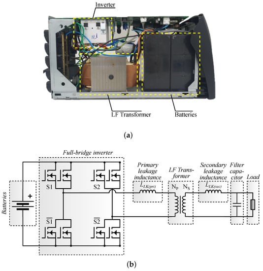
Figure 2.
(a) Commercial line-interactive ferroresonant-based UPS of 1 kW. (b) Offline or line-interactive ferroresonant-based UPS equivalent circuit of operation in backup mode [11].
The three modulation techniques (DM, PS, and DSPLS) are implemented using a dSpace MicroLabBox equipment, base board DS1202. The original microcontroller and control circuits of the commercial UPS are disconnected and replaced by dSpace MicroLabBox via an RJ45 connection to the gate drivers. The use of this equipment allows for alteration of the control and modulation parameters in real time using MATLAB Simulink and Controldesk software. The connection of signals from dSpace via RJ45 is shown in Figure 3.
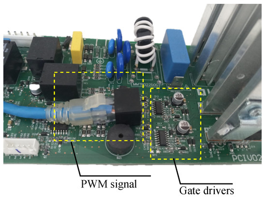
Figure 3.
Connection of signals from dSpace via RJ45 to modify UPS modulation [11].
The UPS is simulated in Simulink, including the inverter topology, the modulation techniques, a model for the transformer impedance, and the resistances of the battery, connectors, and cables. To validate the simulated UPS, Figure 4a,b present the experimental waveforms of current and voltage at the inverter output, with loads of 100 W and 400 W, respectively. Figure 4c,d present the simulated waveforms for the same operation point. In this example, DM is used. The simulated and measured RMS values of voltage and current at the load and at the output of the inverter are compared in Table 1.
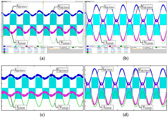
Figure 4.
Waveforms for DM. (a) Experimental 100 W load. (b) Experimental 400 W load. (c) Simulation 100 W load. (d) Simulation 400 W load.

Table 1.
Experimental and simulation RMS voltage and current values, with loads of 100 W and 400 W.
2.2. Losses and Thermal Models
In order to implement the Pareto front analysis, device losses are estimated. MOSFET losses and temperature are mutually dependent, because the drain-source on-state resistance () of the MOSFET is dependent on junction temperature () [30,31,32,33,34]. Thus, accurate models for both are necessary.
Power MOSFET losses may be calculated by analytical methods, SPICE models, or finite element analysis [34,35,36,37]. The use of analytical models is preferable when reduced computational time is desired [32,33,36,37]. In this work, the model presented in [34] is used to estimate conduction and switching losses. Among the models presented in [30,31,34,38,39,40,41], only those presented in [34,38] consider the internal gate resistance, and [34] also takes into account characteristics of the gate driver and the variation of Miller capacitance to determine overlap times. For reverse recovery losses, the model presented in [31] is used.
Device temperature can be estimated using thermal models, which are particular for each application. To obtain the thermal model for the case study UPS, MOSFET temperature variation over time is measured using a Keysight DAQ970A data logger. Thermocouples are placed on the case of the transistor of each pair. The thermocouples used are of the K-type (±2% accuracy).
With the default battery bank of the commercial UPS (7 Ah),the batteries are discharged before the temperature of the MOSFETs reaches a steady-state condition. In order to increase the autonomy of the UPS, an Itech IT7900 programmable voltage source was used to emulate an external battery bank. The resulting MOSFET case temperatures () are shown in Figure 5a,b for the operating points of 400 W and 600 W, respectively.
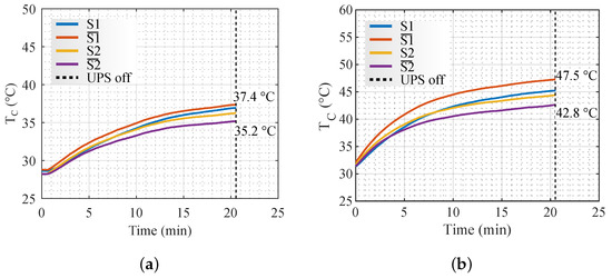
Figure 5.
Temperatures measured in the MOSFETs [11]. (a) 400 W. (b) 600 W.
The behavior of temperature over time is modeled by a parallel RC circuit of equivalent thermal resistance and capacitance [42,43,44,45,46]. The equivalent thermal resistance () is determined using the measured temperature after thermal steady is reached,
at which is the steady state temperature, is the ambient temperature, and P is the device power loss (according to the switching frequency and the power level).
The equivalent thermal capacitance () describes the behavior of temperature as a function of time before a thermal steady-state is reached. This value is determined by extracting an instant in time (t) from the temperature transient,
The values of and obtained from Figure 5 using min are shown in Table 2. Due to the small difference between the values, the average was used. It is observed that in the case that different hardware is used or there are changes in the heat transfer system, and will be different, and thus must be recalculated following the same methodology.
Table 2.
Thermal coefficients calculated [11].
Based on the results presented in Table 2, for the following analysis, the and used for all transistors are 8.4 °C/W and 1 J/°C, corresponding to the respective averages of S1, , S2, and . Thus, only the effect of the modulations on temperatures is analyzed, disregarding the influence of the heat transfer system.
3. Optimization Methodology Considering a Mosfet Database
To evaluate the best cost × efficiency relationship in the full-bridge converter, different part numbers were evaluated. A database with 47 transistors was created (Appendix A), including MOSFETs with rated voltages of 40, 55, and 60 V. All MOSFETs in the database operate safely at the rated power of the UPS system, and two power levels (500 W and 800 W) were used to evaluate the behavior of cost and efficiency in each modulation technique. For the following analysis, all components are compared to the part number that is used in the commercial UPS under study (STP220N6F7). The efficiency of STP220N6F7 is % at 500 W and % at 800 W, and the component costs are normalized with respect to the cost of STP220N6F7 ().
3.1. Discontinuous Modulation
In the Pareto front analysis for DM, two scenarios are considered: (1) all MOSFETs have the same part number, and (2) there are different part numbers for each switching pattern, that is, the transistors in the upper positions are of part number X and the lower ones are of part number Y. Figure 6 depicts these two scenarios.
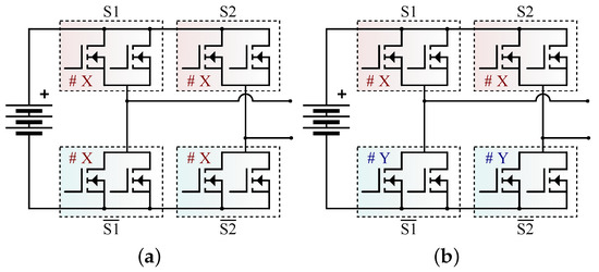
Figure 6.
Inverter part number configuration for DM. (a) Scenario where all MOSFETs have the same part number. (b) Scenario where different part numbers are considered for the different switching patterns.
Figure 7 shows the Pareto front solutions for both scenarios considering the load powers of 500 W and 800 W. The points in red represent the designs relative to scenario 1, and the gray points represent the designs of scenario 2.
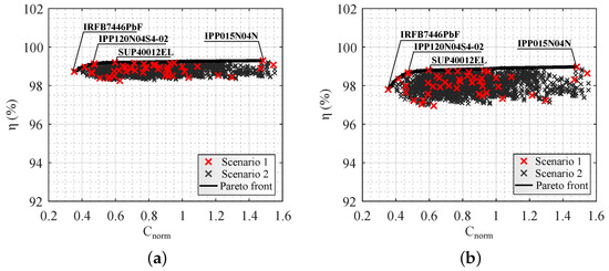
Figure 7.
Pareto front for DM. (a) 500 W. (b) 800 W.
In these, 2209 MOSFET combinations were evaluated. The Pareto front contains the optimal solutions for cost × efficiency. The part numbers on the front are shown in Table 3 and Table 4 for the powers of 500 W and 800 W, respectively, identifying the normalized cost (), efficiency () and junction temperature () for each transistor. The highlighted rows identify the solutions of scenario 1, which uses the same part number in all MOSFETs. These part numbers are presented in Figure 7.
Table 3.
Design details for DM with 500 W.
Table 4.
Design details for DM with 800 W.
The lowest cost solution on the Pareto front for 500 W and 800 W represents 35% of the MOSFET reference cost using the part number IRFB7446PbF. For 500 W, the efficiency achieved is 98.7%, or 0.2% smaller than the reference part number, and for 800 W, % or 0.5% smaller than the reference. The best efficiency condition is obtained with part number IPP015N04N, that being 99.3% in 500 W and 99% in 800 W, with efficiency increases of 0.4% and 0.7% respectively. The cost of this solution is 148% of . The remaining optimal solutions may be selected according to the desired cost × efficiency relationship.
When analyzing , in scenario 1 there is thermal imbalance between the transistors that are off during a half of the fundamental cycle (S1 and S2) and the transistors that are on during a half of the fundamental cycle ( and ). This occurs because DM presents asymmetry in the conduction losses and can result in a reduction in autonomy time according to the operation point [11]. In the optimal designs in scenario 2, the part numbers of the transistors are different, as presented in Figure 6b. The different combinations of MOSFETs result in different losses and consequently differences in behavior. Although and are on during a half of a fundamental cycle, specific combinations of part numbers may result in lower thermal imbalance in the inverter. The lowest difference in is obtained in the design using part number X = IRFB7446PbF and Y = IPP120N04S4-02, where of IRFB7446PbF is 63.4 °C and of IPP120N04S4-02 is 66.9 °C in 800 W.
3.2. Phase-Shifted Modulation
For this modulation technique, the evaluated scenarios are: (1) considering all MOSFETs with the same part number and (2) considering each leg with different part number. Even with symmetric modulation, this scenario is considered in order to evaluate the different combinations of cost × efficiency. Figure 8 shows the configuration of these scenarios for PS modulation: transistors S1 and with part number X and S2 and with part number Y.
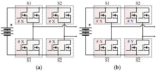
Figure 8.
Inverter part number configuration for PS. (a) Scenario where all MOSFETs have the same part number. (b) Scenario using two different part numbers.
Pareto fronts for PS are shown in Figure 9. The red points represent the designs corresponding to scenario 1, and the green points represent the designs for scenario 2. The part numbers of the optimal solutions are shown in Table 5 and Table 6 for 500 W and 800 W, respectively. The highlighted rows represent the optimal solutions that use the same part number in all MOSFETs.
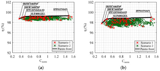
Figure 9.
Pareto front for PS. (a) 500 W. (b) 800 W.
Table 5.
Design details for PS with 500 W.
Table 6.
Design details for PS with 800 W.
The lowest cost solution for 500 W and 800 W is the same as DM, which has 35% of the cost in semiconductors. The best performance condition is also the same as obtained with DM, using part number IPP015N04N. As with the analysis of DM, the remaining optimal solutions may be selected according to the desired cost × efficiency relation.
3.3. Discontinuous Single-Phase Leg Switched Modulation
For DSPLS modulation in scenario 1, all MOSFETs are considered with the same part number, and in scenario 2, different part numbers for each switching pattern (Figure 10). Scenario 2 uses part number X for positions S1 and , which are the transistors that work at the switching frequency (30 kHz), and part number Y for S2 and , which are the transistors that work at the grid frequency.
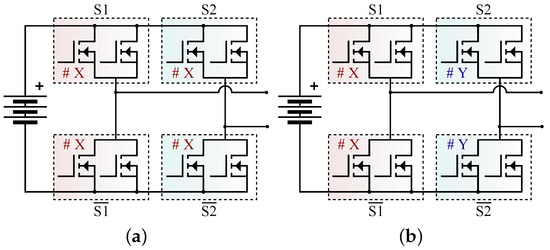
Figure 10.
Inverter part number configuration for DSPLS. (a) Scenario where all MOSFETs have the same part number. (b) Scenario where different part numbers are considered for the different switching patterns.
The Pareto front for DSPLS modulation is shown in Figure 11. The points in red represent the designs corresponding to scenario 1, and the points in blue represent the designs for scenario 2.
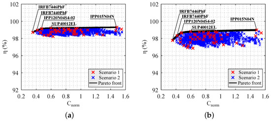
Figure 11.
Pareto front for DSPLS. (a) 500 W. (b) 800 W.
All part numbers of the optimal solutions are shown in Table 7 and Table 8 for the powers of 500 W and 800 W, respectively, identifying the , and obtained with each transistor configuration. The highlighted rows represent the optimal solutions that use only 1 part number in all MOSFETs. These same part numbers are highlighted in Figure 11.
Table 7.
Design details for DSPLS with 500 W.
Table 8.
Design details for DSPLS with 800 W.
The lowest cost MOSFET in the optimal solutions for 500 W and 800 W is the same as the previous modulation techniques, IRFB7446PbF. The highest efficiency optimal solution is obtained with the same part number of DM and PS, IPP015N04N.
For in scenario 1, the lowest thermal imbalance between the high- and low-frequency converter legs at 800 W is 3.3 °C with IRFB7446PbF (). The highest difference in temperature is 6.8 °C with IPP015N04N, even though this is the highest efficiency (99%) optimal solution.
The high efficiency achieved with IPP015N04N is due to its relatively smaller drain-source on-state resistance (). To reduce , manufacturers increase the carrier density and die size, which as a consequence increases internal capacitances. The increase in internal capacitances results in higher switching losses [33], and consequently, there is more thermal imbalance between the legs (only one leg works at high frequency).
In scenario 2 the lowest difference in temperatures between the legs at 800 W is 2.1 °C with part number X = IPP120N04S4-02 and Y = IRFB7440PbF (), and the highest is 15.1 °C with part number X = IRFB7446PbF and Y = IRFB7440PbF ().
4. Comparison of Pareto Front Solutions for the Three Evaluated Modulation Techniques
In the previous sections, the Pareto fronts for each modulation technique were presented as well as several solutions with better efficiencies and attractive costs when compared to the reference. Figure 12 shows the designs and Pareto fronts with the three evaluated modulations together.
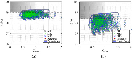
Figure 12.
Pareto front considering all modulation techniques. (a) 500 W. (b) 800 W.
The shaded area contains 403 designs with and . As can be seen in the results of the previous sections, the part numbers found on the front as well as the efficiencies were similar for the three evaluated modulation techniques. However, the analysis of should be used by designers to select the best modulation technique according to the required application. Each modulation technique and part number combination can be exploited according to the heat transfer system used in the converter. For example, thermal imbalance can be desirable if the heat transfer system is asymmetric due to layout constraints.
However, industry applications in general use the same part number in all transistors because of possible advantages in cost (buying in bulk) and uniformity of manufacturing processes. Thus, in this section the analysis of scenario 1 (use of the same part numbers for both converter legs) is emphasized.
In Table 9, the designs with same part numbers in all MOSFETs are shown, detailing the characteristics of voltage rating (), input capacitance (), , , and . The cost is lower than the reference for 80% of selected MOSFETs, being higher only for IPP015N04N. It is possible to identify that as cost increases, decreases and rises. In this evaluation, only transistors with rated voltages of 40 V were selected, instead of 55 V or 60 V transistors. The lower breakdown voltage rating enables smaller die sizes and higher carrier densities in the drift region, which in turn increases electron mobility and reduces the . Thus, the 40 V transistors tend to present higher efficiency and a smaller cost in comparison to 55 V and 60 V transistors. In order to increase the number of solutions, the sub-optimal designs, which are the solutions that are near the Pareto front, are included.
Table 9.
Comparison of optimal solutions with same part number for all MOSFETs with each modulation technique, with 800 W. Reference values: = 1, = 98.23.
Figure 13 shows the designs selected under these conditions, with the center point to the dashed lines being the reference design. The remaining points marked in red are the optimal and sub-optimal designs for scenario 1. Table 10 shows the selected part numbers, detailing the characteristics of , , and . The highlighted rows are the sub-optimal solutions, and the other rows are the optimal solutions that were previously presented.
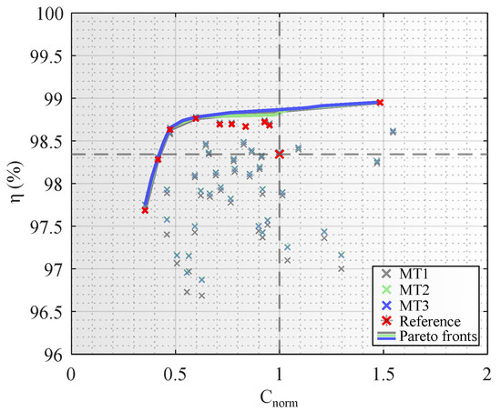
Figure 13.
Pareto front for 800 W considering optimal and sub-optimal designs for scenario 1.
Table 10.
Comparison of optimal and sub-optimal solutions with same part number for all MOSFETs with each modulation technique, for 800 W. Reference values: = 1, = 98.23.
For this evaluation, there are 10 solutions, with 9 having a voltage rating of 40 V, and only one, with the part number SUP50010E, having a voltage rating of 60 V. The normalized cost of this solution is 95% of and improves the efficiency from 98.23% to 98.6%. The 40 V part numbers again were superior in terms of cost × efficiency, as they are manufactured for a lower voltage rating. Among the ten solutions found, once again only the part number IPP015N04N presented a cost higher than .
To evaluate the use of MOSFETs with higher voltage ratings, Figure 14 shows the solutions that use transistors with 40 V. The center point of the dashed lines represents the reference design, and the red line identifies the Pareto front for the transistors with > 40 V. All solutions presented a lower normalized cost than the reference. Table 11 shows the selected part numbers.
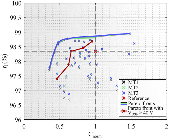
Figure 14.
Pareto front considering MOSFETs with > 40 V, for 800 W.
Table 11.
Comparison of solutions with the same part number in all positions considering only MOSFETs with 40 V for all modulation techniques for 800 W. Reference values: = 1, = 98.23.
The part numbers BUK653R5-55C and IRFB3206PbF showed efficiencies of 0.73% and 0.33% lower than the reference. The normalized costs were 46% and 62%, respectively, which could be an attractive alternative for reducing the cost of semiconductors. The part number IPP024N06N3 showed efficiency similar to the reference value at a cost of 66%. The part numbers SUP50020E and SUP50010E showed a small improvement in efficiency, costing 83% and 95% of the cost, respectively.
5. Conclusions
In this paper, a design of uninterruptible power supply inverters using Pareto front optimization for cost and efficiency was presented. With the use of a MOSFET database, Pareto front analyses were developed considering two different MOSFET combinations in the full-bridge inverter. These were selected according to the switching pattern in DM and DSPLS and considering each leg with a part number in PS in order to evaluate the different combinations of cost × efficiency. In these analyses, the optimal solutions for each modulation technique and its junction temperatures in the MOSFETs were discussed. Based in these results, the designers may select the MOSFET according to the cost, efficiency, and thermal behavior required by the application.
Analysis of scenario 1 (same part numbers for both convert legs) was emphasized in the comparison of the three modulation techniques, because in industry applications, it is the same part number is generally used in all transistors due to advantages in the cost (buying in bulk) and uniformity of the manufacturing processes. The results have showed superior cost × efficiency for MOSFETs manufactured for of 40 V. In order to increase the number of available solutions, sub-optimal solutions were analyzed. Under these conditions, 10 part numbers were selected, where 90% presented of 40 V. In the third analysis, only transistors with 40 V were selected, providing options for applications where there is a demand to use components in this voltage range. Among the three evaluated scenarios and all the solutions found, only the one that uses the IPP015N04N MOSFET has a higher cost than the reference.
Author Contributions
Conceptualization, methodology, validation, writing—original draft, writing—review and editing: E.O.P., P.C.B., H.C.S. and J.R.P.; Supervision: E.O.P., H.C.S. and J.R.P.; Funding acquisition: H.C.S. and J.R.P. All authors have read and agreed to the published version of the manuscript.
Funding
This research was funded by the funding agencies CNPq (process 140848/2020-7) and CAPES (process 88887.597766/2021-00—Financing code 001).
Data Availability Statement
Not applicable.
Conflicts of Interest
The authors declare no conflict of interest. The funders had no role in the design of the study; collection, analyses, or interpretation of data; in the writing of the manuscript, or in the decision to publish the result.
Appendix A
Part numbers in the database are listed: (1) AOT2142L, (2) AUIRF1404Z, (3) AUIRFB8405, (4) DMNH4005SCTQ, (5) STP185N55F3, (6) STP190N55LF3, (7) STP260N6F6, (8) STP220N6F7, (9) FDP020N06-D, (10) FDP025N06-D, (11) FDP030N06B-F102-D, (12) AUIRF1404, (13) IPP120N06S4-H1, (14) IPP015N04N, (15) IPP120N04S4-02, (16) IPP024N06N3, (17) IPP032N06N3, (18) IRFB3206GPbF, (19) IRFB7440PbF, (20) IRFB7446PbF, (21) IRFB3206PbF, (22) IRFB3306PbF, (23) IRL40B215, (24) IPP120N04S3-02, (25) IPP120N04S4-02, (26) AUIRL1404Z, (27) AUIRF3805L, (28) IRL1404PbF, (29) IXTP160N04T2, (30) BUK653R2-55C, (31) BUK653R5-55C, (32) BUK652R6-40C, (33) BUK652R3-40C, (34) PSMN2R1-40PL, (35) PSMN1R5-40PS, (36) PSMN1R9-40PL, (37) PSMN2R0-60PS, (38) PSMN2R5-60PL, (39) PSMN2R6-60PS, (40) PSMN3R9-60PS, (41) PSMN4R2-60PL, (42) SQP120N06-3m5L, (43) SUP40010EL, (44) SUP40012EL, (45) SUP50010E, (46) SUP50020E, (47) SUP50020EL.
References
- IEC62040; Uninterruptible Power Systems (UPS) Part 3: Method of Specifying the Performance and Test Requirements. IEC: Geneva, Switzerland, 1999.
- Kwon, B.H.; Choi, J.H.; Kim, T.W. Improved single-phase line-interactive UPS. IEEE Trans. Ind. Electron. 2001, 48, 804–811. [Google Scholar] [CrossRef]
- Bekiarov, S.B.; Emadi, A. Uninterruptible power supplies: Classification, operation, dynamics, and control. In Proceedings of the APEC. Seventeenth Annual IEEE Applied Power Electronics Conference and Exposition (Cat. No. 02CH37335), Dallas, TX, USA, 10–14 March 2002; Volume 1, pp. 597–604. [Google Scholar]
- Yeh, C.C.; Manjrekar, M.D. A reconfigurable uninterruptible power supply system for multiple power quality applications. IEEE Trans. Power Electron. 2007, 22, 1361–1372. [Google Scholar] [CrossRef]
- Aamir, M.; Kalwar, K.A.; Mekhilef, S. Uninterruptible power supply (UPS) system. Renew. Sustain. Energy Rev. 2016, 58, 1395–1410. [Google Scholar] [CrossRef]
- Iftikhar, M.; Aamir, M.; Waqar, A.; Muslim, F.B.; Alam, I. Line-interactive transformerless uninterruptible power supply (UPS) with a fuel cell as the primary source. Energies 2018, 11, 542. [Google Scholar] [CrossRef]
- Al Kez, D.; Foley, A.M.; Ahmed, F.W.; O’Malley, M.; Muyeen, S. Potential of data centers for fast frequency response services in synchronously isolated power systems. Renew. Sustain. Energy Rev. 2021, 151, 111547. [Google Scholar] [CrossRef]
- Green, P.B. MOSFET Selection for Low Voltage UPS; Infineon Technologies AG: Neubiberg, Germany, 2019; Rev. 1.2. [Google Scholar]
- Green, P.B. Low Frequency Transformer Based SOHO UPS Design; Infineon Technologies AG: Neubiberg, Germany, 2020; Rev. 1.1. [Google Scholar]
- Ahmed, K.M.U.; Bollen, M.H.; Alvarez, M. A Review of Data Centers Energy Consumption And Reliability Modeling. IEEE Access 2021, 9, 152536–152563. [Google Scholar] [CrossRef]
- Prado, E.O.; Bolsi, P.C.; Sartori, H.C.; Pinheiro, J.R. Comparative Analysis of Modulation Techniques on the Losses and Thermal Limits of Uninterruptible Power Supply Systems. Micromachines 2022, 13, 1708. [Google Scholar] [CrossRef] [PubMed]
- Zhou, Z.J.; Zhang, X.; Xu, P.; Shen, W.X. Single-phase uninterruptible power supply based on Z-source inverter. IEEE Trans. Ind. Electron. 2008, 55, 2997–3004. [Google Scholar] [CrossRef]
- Racine, M.S.; Parham, J.D.; Rashid, M. An overview of uninterruptible power supplies. In Proceedings of the 37th Annual North American Power Symposium, Ames, IA, USA, 25 October 2005; pp. 159–164. [Google Scholar]
- Rahmat, M.K.; Jovanovic, S.; Lo, K.L. Reliability estimation of uninterruptible power supply systems: Boolean truth table method. In Proceedings of the INTELEC 06-Twenty-Eighth International Telecommunications Energy Conference, Providence, RI, USA, 10–14 September 2006; pp. 1–6. [Google Scholar]
- Rahmat, M.K.; Jovanovic, S.; Lo, K.L. Reliability and Availability modelling of Uninterruptible Power Supply (UPS) systems using Monte-Carlo simulation. In Proceedings of the 2011 5th International Power Engineering and Optimization Conference, Shah Alam, Malaysia, 6–7 June 2011; pp. 267–272. [Google Scholar]
- Rahmat, M.K.; Karim, A.Z.A.; Salleh, M.N.M. Sensitivity analysis of the AC uninterruptible power supply (UPS) reliability. In Proceedings of the 2017 International Conference on Engineering Technology and Technopreneurship (ICE2T), Kuala Lumpur, Malaysia, 18–20 September 2017; pp. 1–6. [Google Scholar]
- Holmes, D.G.; Lipo, T.A. Pulse Width Modulation for Power Converters: Principles and Practice; John Wiley & Sons: Hoboken, NJ, USA, 2014. [Google Scholar]
- Erickson, R.W.; Maksimovic, D. Fundamentals of Power Electronics; Springer Science & Business Media: Berlin/Heidelberg, Germany, 2007. [Google Scholar]
- Rashid, M.H. Power Electronics: Circuits, Devices, and Applications; Butterworth-Heinemann: Burlington, MA, USA, 2009. [Google Scholar]
- Bernacki, K.; Rymarski, Z. Electromagnetic compatibility of voltage source inverters for uninterruptible power supply system depending on the pulse-width modulation scheme. IET Power Electron. 2015, 8, 1026–1034. [Google Scholar] [CrossRef]
- Busquets-Monge, S.; Crebier, J.C.; Ragon, S.; Hertz, E.; Boroyevich, D.; Gurdal, Z.; Arpilliere, M.; Lindner, D.K. Design of a boost power factor correction converter using optimization techniques. IEEE Trans. Power Electron. 2004, 19, 1388–1396. [Google Scholar] [CrossRef]
- Biela, J.; Kolar, J.W.; Deboy, G. Optimal design of a compact 99.3% efficient single-phase PFC rectifier. In Proceedings of the 2010 Twenty-Fifth Annual IEEE Applied Power Electronics Conference and Exposition (APEC), Palm Springs, CA, USA, 21–25 February 2010; pp. 1397–1404. [Google Scholar]
- Sartori, H.C.; Hey, H.L.; Pinheiro, J.R. An optimum design of PFC Boost Converters. In Proceedings of the 2009 13th European Conference on Power Electronics and Applications, Barcelona, Spain, 8–10 September 2009; pp. 1–10. [Google Scholar]
- Chen, B.; Gu, B.; Zhang, L.; Zahid, Z.U.; Lai, J.S.; Liao, Z.; Hao, R. A high-efficiency MOSFET transformerless inverter for nonisolated microinverter applications. IEEE Trans. Power Electron. 2014, 30, 3610–3622. [Google Scholar] [CrossRef]
- Sartori, H.C.; Baggio, J.E.; Hey, H.L.; Pinheiro, J.R.; Beltrame, F. Integrated methodology design to improve the efficiency and reduce volume of the CCM PFC boost converters with pre-sizing settings. In Proceedings of the 2015 IEEE 24th International Symposium on Industrial Electronics (ISIE), Buzios, Brazil, 3–5 June 2015; pp. 1378–1385. [Google Scholar]
- Bolsi, P.C.; Prado, E.O.; Sartori, H.C.; Lenz, J.M.; Pinheiro, J.R. LCL Filter Parameter and Hardware Design Methodology for Minimum Volume Considering Capacitor Lifetimes. Energies 2022, 15, 4420. [Google Scholar] [CrossRef]
- Kolar, J.W.; Biela, J.; Minibock, J. Exploring the pareto front of multi-objective single-phase PFC rectifier design optimization-99.2% efficiency vs. 7kW/din 3 power density. In Proceedings of the 2009 IEEE 6th International Power Electronics and Motion Control Conference, Wuhan, China, 17–20 May 2009; pp. 1–21. [Google Scholar]
- Louvrier, Y.; Barrade, P.; Rufer, A. Weight and efficiency optimization strategy of an interleaved DC-DC converter for a solar aircraft. In Proceedings of the 2009 13th European Conference on Power Electronics and Applications, Barcelona, Spain, 8–10 September 2009; pp. 1–10. [Google Scholar]
- STMicroelectronics. N-Channel 60 V Power MOSFET in a TO-220 Package, STP220N6F7; STMicroelectronics: Geneva, Switzerland, 2015; Rev. 3. [Google Scholar]
- Lakkas, G. MOSFET power losses and how they affect power-supply efficiency. Analog Appl 2016, 10, 22–26. [Google Scholar]
- Graovac, D.; Purschel, M.; Kiep, A. MOSFET power losses calculation using the data-sheet parameters. Infineon Appl. Note 2006, 1, 1–23. [Google Scholar]
- Prado, E.O.; Sartori, H.C.; Pinheiro, J.R. How to select power transistors for static converters applications? In Proceedings of the 2018 13th IEEE International Conference on Industry Applications (INDUSCON), Sao Paulo, Brazil, 12–14 November 2018; pp. 138–143. [Google Scholar]
- Prado, E.O.; Bolsi, P.C.; Sartori, H.C.; Pinheiro, J.R. An Overview about Si, Superjunction, SiC and GaN Power MOSFET Technologies in Power Electronics Applications. Energies 2022, 15, 5244. [Google Scholar] [CrossRef]
- Prado, E.O.; Bolsi, P.C.; Sartori, H.C.; Pinheiro, J.R. Simple analytical model for accurate switching loss calculation in power MOSFETs using non-linearities of Miller capacitance. IET Power Electron. 2022, 15, 594–604. [Google Scholar] [CrossRef]
- Xiao, Y.; Shah, H.; Chow, T.; Gutmann, R. Analytical modeling and experimental evaluation of interconnect parasitic inductance on MOSFET switching characteristics. In Proceedings of the Nineteenth Annual IEEE Applied Power Electronics Conference and Exposition, 2004. APEC’04, Anaheim, CA, USA, 22–26 February 2004; Volume 1, pp. 516–521. [Google Scholar]
- Ren, Y.; Xu, M.; Zhou, J.; Lee, F.C. Analytical loss model of power MOSFET. IEEE Trans. Power Electron. 2006, 21, 310–319. [Google Scholar]
- de Paula, W.J.; Tavares, G.H.M.; Soares, G.M.; Almeida, P.S.; Braga, H.A.C. Switching losses prediction methods oriented to power MOSFETs–a review. IET Power Electron. 2020, 13, 2960–2970. [Google Scholar] [CrossRef]
- Brown, J. Modeling the switching performance of a MOSFET in the high side of a non-isolated buck converter. IEEE Trans. Power Electron. 2006, 21, 3–10. [Google Scholar] [CrossRef]
- Sartori, H.C.; Beltrame, F.; Figueira, H.H.; Baggio, J.E.; Pinheiro, J.R. Power density comparative analysis concerning to three transistor technologies applied to a CCM PFC BOOST converter using optimization techniques. In Proceedings of the 2013 Brazilian Power Electronics Conference, Gramado, Brazil, 27–31 October 2013; pp. 1317–1323. [Google Scholar]
- Beltrame, F.; Dupont, F.H.; Sartori, H.C.; Cancian, E.C.; Rech, C.; Pinheiro, J.R. Efficiency optimization of DC/DC boost converter applied to the photovoltaic system. In Proceedings of the IECON 2013-39th Annual Conference of the IEEE Industrial Electronics Society, Vienna, Austria, 10–13 November 2013; pp. 706–711. [Google Scholar]
- Guo, J.; Ge, H.; Ye, J.; Emadi, A. Improved method for MOSFET voltage rise-time and fall-time estimation in inverter switching loss calculation. In Proceedings of the 2015 IEEE Transportation Electrification Conference and Expo (ITEC), Dearborn, MI, USA, 14–17 June 2015; pp. 1–6. [Google Scholar]
- Seshasayee, N. Understanding Thermal Dissipation and Design of a Heatsink; Texas Instruments: Dallas, TX, USA, 2011; pp. 1–4. [Google Scholar]
- Chen, H.; Ji, B.; Pickert, V.; Cao, W. Real-time temperature estimation for power MOSFETs considering thermal aging effects. IEEE Trans. Device Mater. Reliab. 2013, 14, 220–228. [Google Scholar] [CrossRef]
- Yang, K.; Guo, J.; Ge, H.; Bilgin, B.; Loukanov, V.; Emadi, A. Transient electro-thermal analysis for a MOSFET based traction inverter. In Proceedings of the 2014 IEEE Transportation Electrification Conference and Expo (ITEC), Beijing, China, 31 August–3 September 2014; pp. 1–6. [Google Scholar]
- On Semiconductor. Heat Sink Selection Guide for Thermally Enhaced SO8-FL; On Semiconductor: Phoenix, AZ, USA, 2015; Rev. 1. [Google Scholar]
- Melito, M.; Gaito, A.; Sorrentino, G. Thermal effects and junction temperature evaluation of Power MOSFETs. DocID028570 Rev. 2015, 1, 141. [Google Scholar]


Disclaimer/Publisher’s Note: The statements, opinions and data contained in all publications are solely those of the individual author(s) and contributor(s) and not of MDPI and/or the editor(s). MDPI and/or the editor(s) disclaim responsibility for any injury to people or property resulting from any ideas, methods, instructions or products referred to in the content. |
© 2023 by the authors. Licensee MDPI, Basel, Switzerland. This article is an open access article distributed under the terms and conditions of the Creative Commons Attribution (CC BY) license (https://creativecommons.org/licenses/by/4.0/).