Article

A Triple Boost Seven-Level Common Ground Transformerless Inverter Topology for Grid-Connected Photovoltaic Applications

by
Narayanan Pandurangan Gopinath
1,
Krishnasamy Vijayakumar
1,
Jagabar Sathik Mohd Ali
2,*,
Kumutha Raghupathi
3 and
Sivakumar Selvam
2
1
Department of Electrical and Electronics Engineering, SRM Institute of Science and Technology, Kattankulathur, Chennai 603203, India
2
Renewable Energy Lab, College of Engineering, Prince Sultan University, Riyadh 11586, Saudi Arabia
3
Department of Physics, S.A. Engineering College, Chennai 600077, India
*
Author to whom correspondence should be addressed.
Energies 2023, 16(8), 3428; https://doi.org/10.3390/en16083428
Submission received: 8 March 2023 / Revised: 24 March 2023 / Accepted: 7 April 2023 / Published: 13 April 2023

Abstract

:
This article proposes a single-stage, seven-level (7L), switched-capacitor-based grid-connected inverter architecture with a common ground feature. This topology has the ability to boost the output voltage up to three times the input voltage. The proposed topology can diminish the leakage current in grid-connected photovoltaic (GC-PV) applications, and its capacitor voltages are self-balanced without any additional control strategies. The different operating modes are described in detail with their related mathematical expressions. The design of passive components and a detailed power loss analysis are presented. The merits of the proposed structure are demonstrated using a detailed comparative assessment. The grid-connected operation of the proposed inverter structure is simulated in the MATLAB/Simulink environment, and the results are presented. The laboratory prototype of 935 W is built and analyzed to validate the performance of the proposed structure.

1. Introduction

The multilevel inverters are well matured and developed technology for various applications [1,2,3,4]. In recent years, transformerless (TL) inverters have replaced transformers in GC-PV systems due to their decreased cost, smaller size, and improved efficiency [5]. The removal of transformers, however, results in leakage current flow, which causes several issues, such as increased current harmonic distortion, personal safety, power quality, and electromagnetic interferences [6]. Additionally, in PV energy applications, the input voltage needs to be boosted, which gets rid of the front-end boost converter and makes the whole system more efficient. Thus, extensive research efforts have been carried out in recent years to develop TL inverter topologies with the inherent voltage-boosting ability and to eliminate the leakage current in photovoltaic applications [7]. Many TL inverter topologies have been proposed, such as the mid-point clamping method and decoupling (DC and AC) methods. However, they cannot eliminate the leakage current and can also not boost the input voltage [8,9]. A neutral point clamp-based quasi-Z-Source T-Type inverter using eight switches, four inductors, four capacitors, and four diodes was presented in [10]. This topology requires EMI filters to minimize high-frequency variation in CMV, increasing the cost of the inverter. Additionally, it requires a high number of power components to generate a five-level AC output voltage waveform with unity voltage gain. In [11], switched-boost inverter (SBI) topologies are proposed. It uses only half of the passive components compared to impedance-source inverters. However, the high voltage stress on the capacitor and lower boost factor than the impedance source topologies are the demerits of the SBI topologies. In [12], the quasi-switched-boost inverter (qSBI)-type topology was presented. When comparing the qSBI with qZSI, the capacitance of qZSI is fourfold that of qSBI, and the DC-link boost factor of qSBI is higher than that of qZSI. However, the high common-mode voltage generation in qSBI topologies makes them unsuitable for transformerless PV applications [13]. The common ground (CG)-type TL inverter topologies effectively eliminate the leakage current in GC-PV systems [14,15]. Here, the neutrality of the grid and negative terminal of the input PV source are connected to a common ground, as shown in Figure 1. In addition to leakage current elimination, the other aim, i.e., voltage boosting ability in transformerless inverter topology, is achieved by incorporating switched capacitors (SCs) into its structure. In [16], a family of flying capacitor-based CG-TL (type-I, type-II, and Type-III) inverter topologies are presented. Here, the maximum number of output voltage levels is three, and the maximum output voltage is equal to the input voltage. The topology [17] proposes a charge pump concept in the transformerless inverter. Since the negative output voltage level solely depends on this charge pump circuit, that may result in a requirement of the DC to offset compensation. CG-TL inverter topology based on a flying capacitor is presented in [18] to eliminate leakage current. It generates a five-level (5L) output voltage with unity voltage gain using six switches, one diode, and two capacitors. Here, to balance their capacitor voltages, their design needs to employ additional control approaches.
The author of [18] proposed another 5L CG-TL inverter topology [19] that uses seven switches and three capacitors. However, the voltage gain is still one, requiring additional sensors for their capacitor voltage balancing, which increases the cost. The topology proposed in [20] can eliminate leakage current but does not increase output voltage; additionally, like topologies [18,19], this requires voltage sensors to balance their capacitor voltage, which increases the cost. The topology suggested in [21] uses two capacitors, one of which is a switched capacitor and the other is a flying capacitor. Here, a small inductor is inserted in the capacitor charging loop; thereby, reducing the inrush current. Even though the topologies presented in [16,17,18,19,20,21] effectively eliminate leakage current due to their CG-type structure, they fail to boost the output voltage. In recent years, various topologies [22,23,24,25,26,27] with boosting ability have been proposed to address this shortcoming. Although the topology [22] can increase the voltage up to twice the input voltage, it suffers from high-current stresses on the semiconductor devices and necessitates high-rated capacitors. In [23], a dual boost CG-type inverter topology with soft charging is presented. This reduces the charging current ripples across the capacitors. The topologies [24,25,26,27] are similar and generate double voltage boosting at the inverter output terminals. The above topologies require either one of the capacitor voltages to be rated twice that of the input voltage. In topologies [24,25], the maximum blocking voltage (MBV) across four switches is double the source voltage, while three switches have an MBV of twice the input voltage [26,27]. Recently, CG-TL topologies with integrated boost cells have been proposed [28,29,30]. In these topologies, dynamic voltage boosting is achieved by varying the duty cycle of the integrated boost cell switch. The topology [28] uses seven switches, two diodes, and three capacitors to achieve a 5L output voltage. Since the duty cycle of the integrated boost cell switch is kept at 50%, the boosting factor of this topology is 4. Here, each of the three switched capacitors has to be rated at twice the input voltage, and the maximum blocking voltage of the semiconductor switch is four times the source voltage. Similar to topology [28], the topology presented in [29] also generates 5L output voltage at the cost of an increased number of semiconductor devices. In this case, the main cons are the maximum blocking voltage and the rating of switched capacitors. Another 5L CG-TL structure with an integrated boost cell is proposed in [30]. Here, keeping the duty cycle of the integrated boost cell switch at 50% yields a voltage gain of 2, which is equivalent to 4 in topologies [28,29]. Additionally, five of the eight power semiconductor switches have a voltage stress equal to the boosted output voltage, and the voltage stress on the capacitors is uneven. The CG-TL inverter topologies presented in [31,32] generate a 9L waveform with a voltage gain of 2. Here, also, the voltage stress on the utilized capacitors is uneven. Another 9L CG-type topology is proposed in [33]. This topology is capable of a voltage boosting of 4. The drawbacks of this topology are higher switch voltage stress and uneven voltage stress on the utilized capacitors. To overcome the shortcomings of the voltage boosting ability, the higher voltage stress on switches, and the uneven voltage stress on capacitors, this article is proposing the following key features:
(i).
Single-phase single-stage 7L CG-type inverter that can diminish the leakage current.
(ii).
The voltage gain is 3.
(iii).
The voltage stress of capacitors is even, i.e., equal to the input voltage, Vin.
(iv).
The MBV is equal to 2/3 of the output voltage.
(v).
Capacitors are self-balanced.
(vi).
The proposed topology is capable of reactive power support.

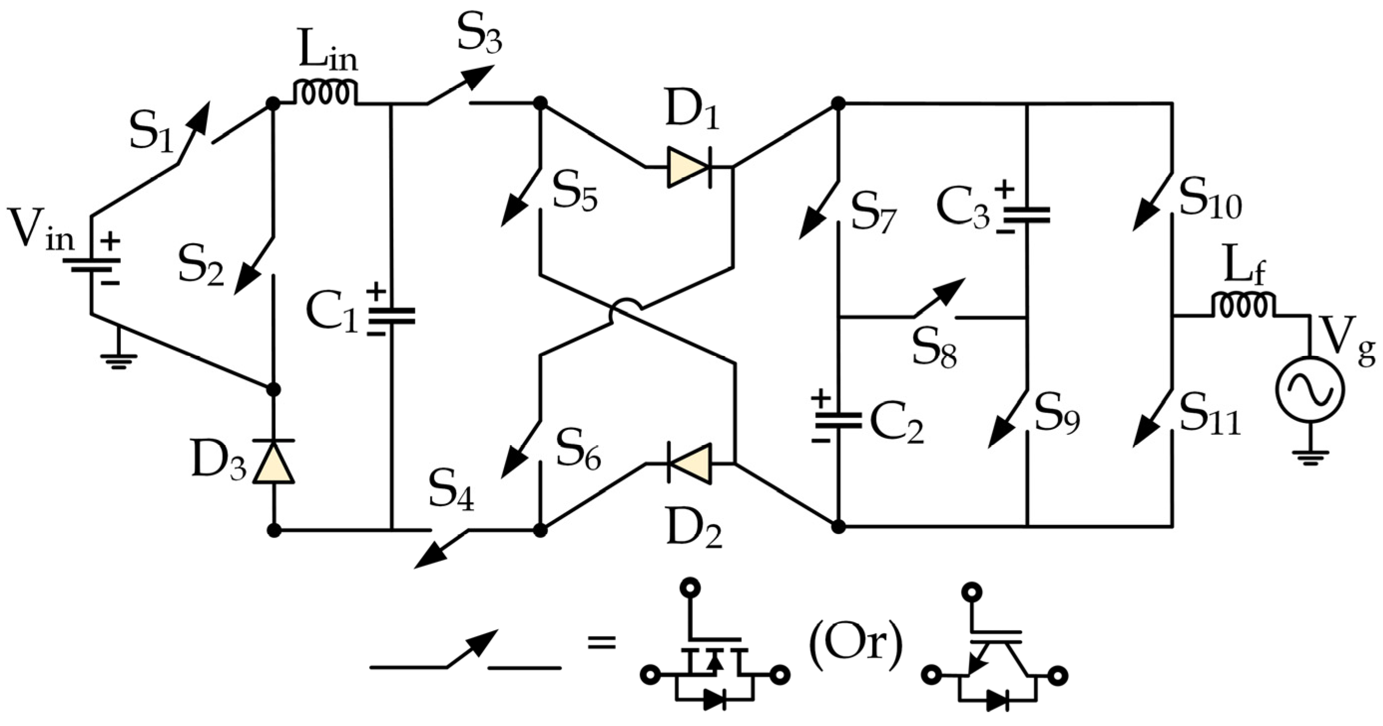
2. Proposed 7LCG-TL Inverter

2.1. Description of 7LCG-TL Inverter

Figure 2 depicts the proposed 7LCG-TL inverter topology. The proposed structure utilizes eleven unidirectional power semiconductor switches (S1–S11), three diodes (D1–D3), and three switched capacitors (C1–C3) to generate 7L output voltage with levels of +3Vin, +2Vin, +Vin, 0, −Vin, −2Vin, and −3Vin. When switch S1 is ON, and S2 is OFF, the parallel connection of the source and SC-C1 charges the capacitor to the input voltage Vin. Similarly, the other two SCs C2 and C3 are also charged up to the input voltage Vin when they are connected in parallel with the source. Since the proposed topology integrates the utility grid and photovoltaic system, the PV panel is considered the source of the inverter.

2.2. Description of Modes of Operation

As per the switching sequence given in Table 1, all seven levels of the 7LCG-TL with its conductive path are shown in Figure 3a–g. The values ‘0’ and ‘1’ in Table 1, represent the OFF and ON states of corresponding switches. The charging path of the capacitor C1 is represented by the purple dotted line and the other two capacitors C2 and C3 are represented by the green dotted line. The functioning of various operating modes of the proposed topology is described as follows:

2.2.1. Maximum Positive Output Voltage Level (+3Vin)

Figure 3a depicts the proposed inverter’s maximum output voltage level. Here, the SC-C1 is in parallel with the source via the switch S1 and diode D3 and is, therefore, charged to Vin. During this mode of operation, the source voltage Vin is connected in series with the capacitors C1 and C2 to generate a maximum output voltage of +3Vin.
This can be achieved by turning on the switches S1, S3, S5, S8, and S10. The mathematical expression for output voltage is written as
V o = V i n + V C 2 + V C 3 = 3 V i n
The current stress of the switches is written as
i S 3 = i S 5 = i S 8 = i S 10 = i g d ( t ) i g d ( t ) = I g , p k sin ( ω t ) i S 1 = i i n = I c h a r , C 1 + i g d ( t )
where  i g d ( t ) I g , p k  are the grid current and its peak value, and  I c h a r , C 1  is the capacitor C1 charging current.

2.2.2. Second Positive Output Voltage Level (+2Vin)

This mode of operation is obtained using the series connection between the input and the capacitor C2 voltage. The switches S1, S3, S5, S7, and S10 are turned ON as shown in Figure 3b. The inverter’s output voltage is mathematically written as
V o = V i n + V C 2 = 2 V i n
The current stress of the switches is written as
i S 3 = i S 5 = i S 7 = i S 10 = i g d ( t ) i g d ( t ) = I g , p k sin ( ω t ) i S 1 = i i n = I c h a r , C 1 + i g d ( t )

2.2.3. First Positive Output Voltage Level (+Vin)

The equivalent circuit to generate the first positive output voltage level is shown in Figure 3c. This level is achieved by triggering ON the switches S1, S3, and S10. Additionally, the switches S4, S7, and S9 are triggered ON to charge the capacitors C2 and C3. The mathematical expression for the output voltage is
V o = V i n V C 2 = V C 3 = V i n
The current stress of the switches is written as
i S 3 = i S 5 = i S 7 = i S 10 = i g d ( t ) i g d ( t ) = I g , p k sin ( ω t ) i S 1 = i i n = I c h a r , C 1 + i 1 i 1 = I c h a r , C 2 + I c h a r , C 3 + i g d ( t ) i 7 = I c h a r , C 2 ;   i 9 = I c h a r , C 3

2.2.4. Zero Output Voltage Level (0)

In this mode of operation, the zero-output voltage is obtained by turning ON the switches S4 and S11 as shown in Figure 3d. Additionally, switches S1, S3, S7, and S9 are triggered ON to charge the three SCs.
The current stress of the switches is written as
i S 11 = i g d ( t ) = I g , p k sin ( ω t ) i S 1 = i i n = I c h a r , C 1 + i 1 i 1 = I c h a r , C 2 + I c h a r , C 3 i 7 = I c h a r , C 2 ;   i 9 = I c h a r , C 3

2.2.5. First Negative Output Voltage Level (−Vin)

Figure 3e illustrates this mode of operation. The capacitor C2 is discharged to generate this first negative output voltage by switching ON the switches S4, S6, S7, and S11. The SC-C1 is charged through switch S1, whereas the capacitor C3 is bypassed from the circuit. Here, the inverter output voltage equation is
V o = V C 2 = V i n
The current stress of the switches is written as
i S 4 = i S 6 = i S 7 = i S 11 = i g d ( t ) i g d ( t ) = I g , p k sin ( ω t ) i S 1 = i i n = I c h a r , C 1

2.2.6. Second Negative Output Voltage Level (−2Vin)

The current flow path for this mode of operation is illustrated in Figure 3f. The capacitors C1 and C3 are connected in series through the switches S2, S4, S6, S9, and S11, and the inverter output voltage equation is written as
V o = ( V C 1 + V C 3 ) = 2 V i n
The current stress of the switches is written as
i S 2 = i S 4 = i S 6 = i S 9 = i S 11 = i g d ( t ) i g d ( t ) = I g , p k sin ( ω t )

2.2.7. Maximum Negative Output Voltage Level (−3Vin)

The negative maximum voltage level of the proposed structure is obtained, as depicted in Figure 3g. Here, the capacitors C1, C3, and C3 are connected in series to supply power to the grid. This can be achieved by the on-state switches S2, S4, S6, S8, and S11. The output voltage equation is expressed as follows:
V o = ( V C 1 + V C 2 + V C 3 ) = 3 V i n
The current stress equations of the switches are expressed as
i S 2 = i S 4 = i S 6 = i S 8 = i S 11 = i g d ( t ) i g d ( t ) = I g , p k sin ( ω t )
The voltage stress of all switches during different operating modes is summarized and presented in Table 2. From the working of the proposed structure and Table 2, the MBV and total standing voltage per unit (TSVp.u.) can be obtained as
M B V = 2 V i n
T S V p . u . = x = 1 11 V s x V o , m x = 5

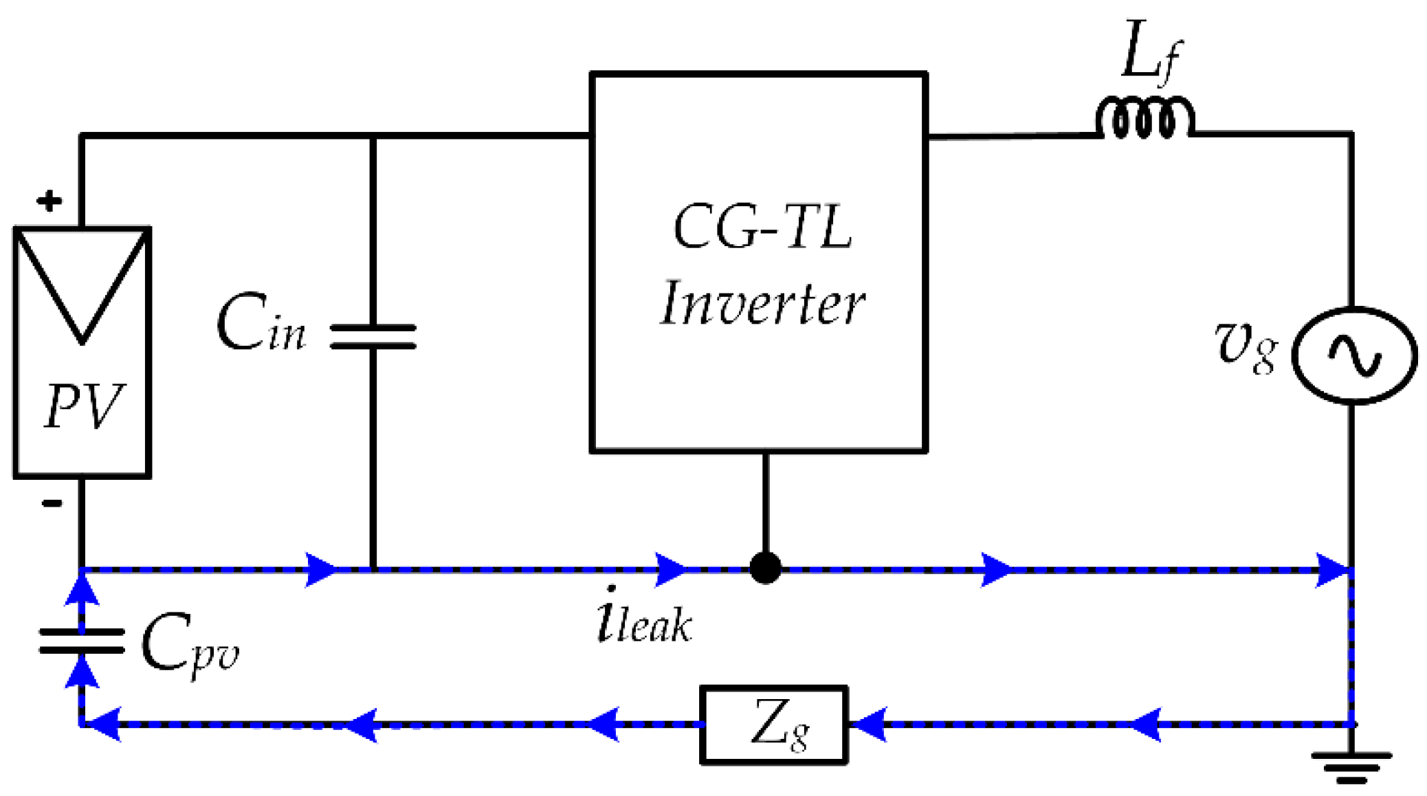
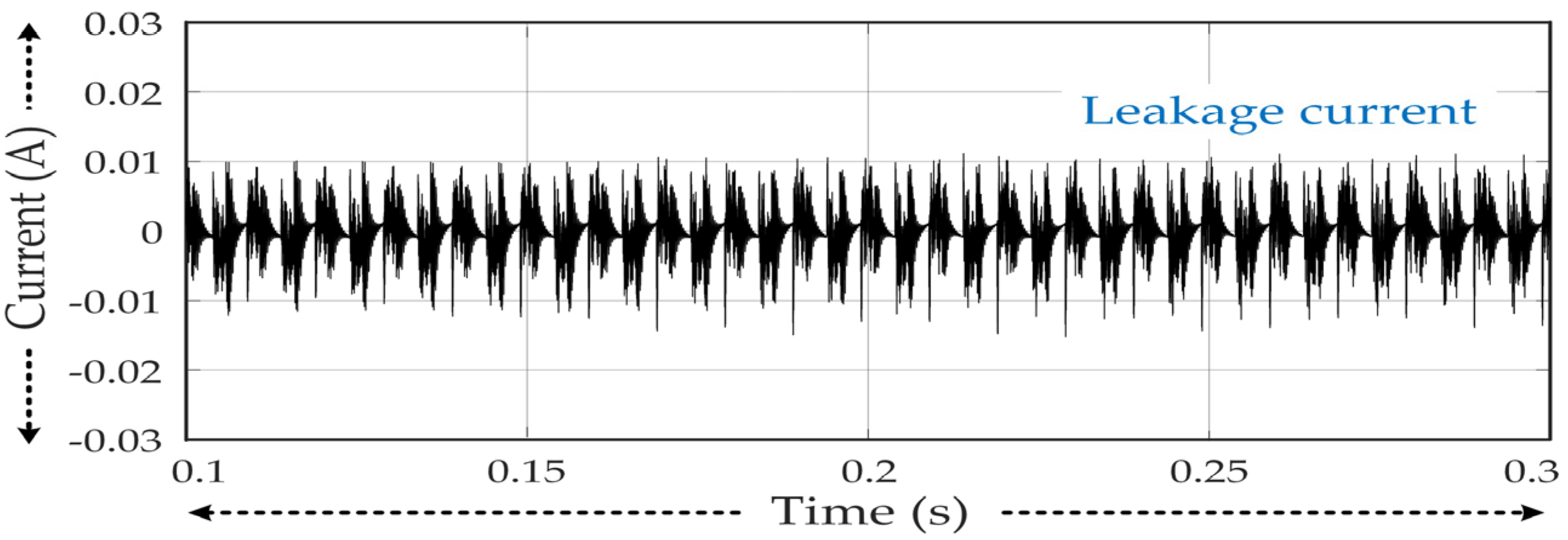
2.3. Common Mode Analysis

The common-mode behavior of the proposed topology is analyzed using a generalized common-mode circuit [6], as shown in Figure 4a. Concerning the voltage between the output terminals x and y and a common reference N, as shown in Figure 4a, the common mode voltage of the converter is expressed as [19]
V C M = V x N + V y N 2 + V x N V y N L n L m 2 ( L n + L m )
where x and y represent the output terminals of the inverter and N is the common reference. As can be seen from Figure 4b, the negative terminal of the proposed topology is directly connected to the neutral of the grid resulting in VyN = 0. Additionally, there is only one output inductor, i.e., Ln = 0, as shown in Figure 4b. By assuming the low ground impedance Zg, the parasitic capacitance CPV from the PV side to the earth is connected by the common AC and DC ground. By substituting VyN = 0 and Ln = 0 in (16), the common voltage VCM synthesized by the inverter is obtained as follows
V C M = V x N V x N 2 = 0
It is clear from (17) that the suggested topology produces a constant zero common-mode voltage and does not exhibit any high-frequency component; the inverter practically ensures the suppression of the ground current.

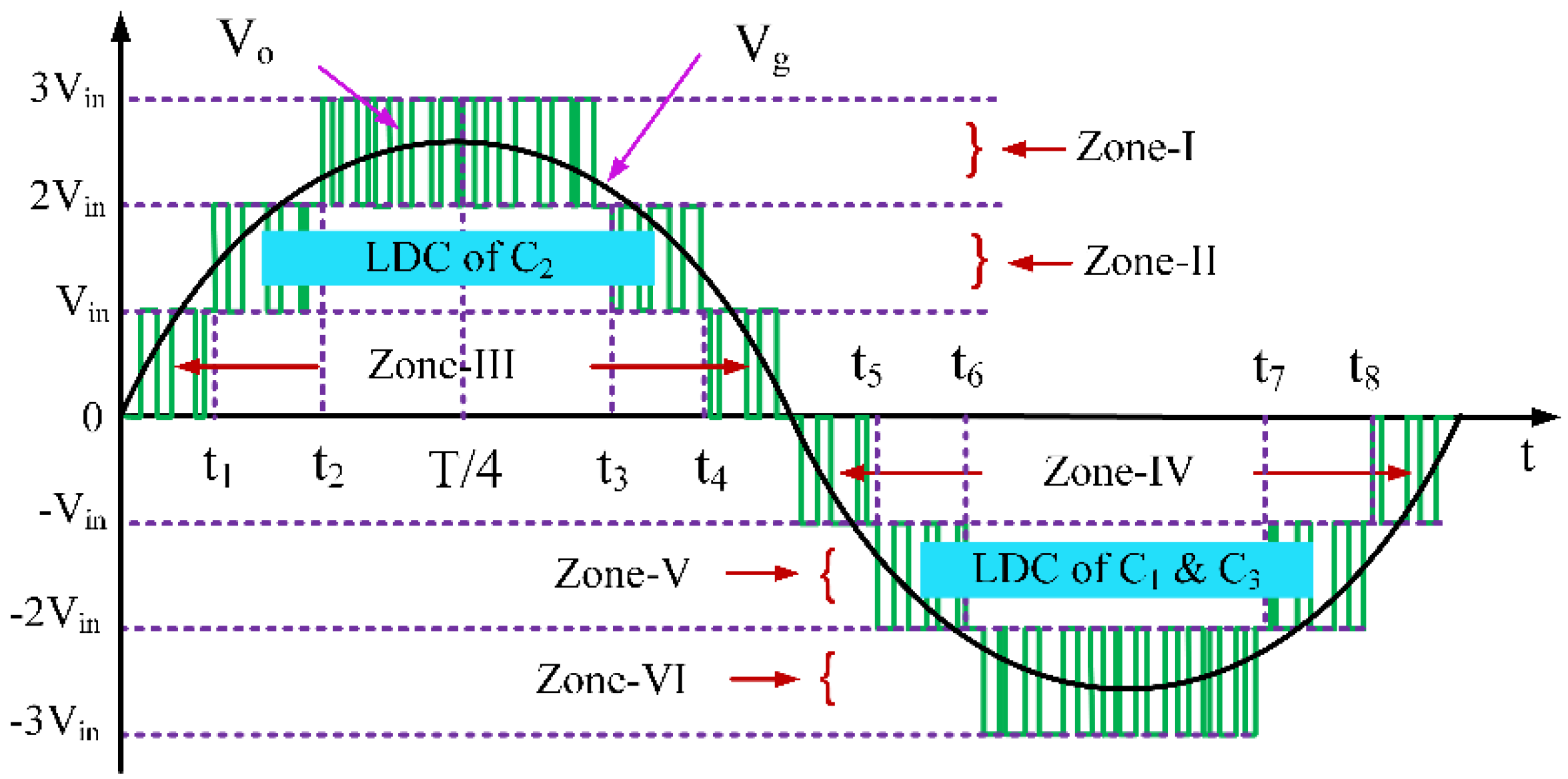
3. Calculation of Duty Cycle of Switches

Figure 5 shows the 7L inverter output voltage (Vo) along with the grid-voltage (Vg) waveform. It can be seen that there are six operating zones (Zone-I to Zone-VI). The control method [25] of the proposed topology is obtained based on Figure 3. By applying the inductor volt-second balanced (V-S B) principle for the output inductor over one full operating time period (Ts), the duty cycle of the switches in different operating zones can be calculated. The grid voltage and grid current equations can be written as
v g ( t ) = V g , p k sin ( ω t ) i g d ( t ) = I g , p k sin ( ω t )
where  V g , p k ,   and   I g , p k  represent the peak value of grid voltage and current.

3.1. Zone-I

As seen in Figure 5, the output voltage varies between 0 and Vin during Zone-I. By using the (V-S B) law for inductor  L f , the duty cycle (d1) for the operating zone-I can be calculated as (19) and (20):
0 d 1 T s ( V i n v g )   d t + d 1 T s T s ( v g )   d t = 0 ;   0 t t 1
d 1 ( t ) = v g V i n   = V g , p k sin ( ω t ) V i n ;   0 t t 1

3.2. Zone-II

As seen in Figure 5, during the time interval  t 1   to   t 2   and   t 3   to   t 4 , i.e., Zone-II, the inverter’s output voltage varies between Vin and 2Vin. By using the (V-S B) law for inductor  L f , the duty cycle (d2) for the operating zone-II can be calculated as (21) and (22):
0 d 2 T s ( 2 V i n v g )   d t + d 2 T s T s ( V i n v g )   d t = 0 ;   t 1 t t 2
d 2 ( t ) = v g V i n 1   = d 1 ( t ) 1 = V g , p k sin ( ω t ) V i n 1 ;   t 1 t t 2

3.3. Zone-III

It is observed from Figure 5 that, during the interval  t 2   to   t 3 , i.e., Zone-III, the output voltage of the inverter varies in between 2Vin and 3Vin. By using the (V-S B) law for inductor  L f , the duty cycle (d3) for the operating zone-III can be calculated as (23) and (24):
0 d 3 T s ( 3 V i n v g )   d t + d 3 T s T s ( 2 V i n v g )   d t = 0 ;   t 2 t t 3
d 3 ( t ) = v g V i n 2   = d 1 ( t ) 2 = V g , p k sin ( ω t ) V i n 2 ;   t 2 t t 3

4. Design of Passive Elements

To obtain the value of the output inductor filter  L f  based on the current flowing through the filter inductor  i L f ( t ) , the output inductor current ripple is written as
i L f = i L f ( t = d 3 T s ) i L f ( 0 ) = 3 V i n v g d 3 L f f s ;   t 2 t t 3
From Equations (24) and (25):
L f   = 1 i L f f s   5 V g , p k sin ( ω t ) 6 V i n V 2 g , p k sin 2 ( ω t ) V i n
The inductor current ripple is maximum when the grid voltage is at its peak value, and, thus, the respective  L f  value can be calculated as
L f   = 1 i L f , m x   × f s   5 V g , p k 6 V i n V 2 g , p k V i n
The required values of the utilized capacitors C1, C2, and C3 are calculated based on their longest discharge duration (LDC) over one full cycle. Figure 3a–g and Figure 4 show that the LDC of the capacitors C1 and C3 is between    t 5   and   t 8   , and C2 is between    t 1   and   t 4 . Thus, the charge on capacitors C1, C2, and C3 during their LDC time can be written as
Q C 2 = t 1 t 4 I g , p k sin ( ω t ) Q C 1 = Q C 3 = t 5 t 8 I g , p k sin ( ω t ) = t 1 t 4 I g , p k sin ( ω t )
Q C = Q C 1 = Q C 2 = Q C 3 =   I g , p k ω × cos ( ω t 1 ) cos ( ω t 4 )
Q C x = C x × V C x
C = C 1 = C 2 = C 3 = Q C V C = I g , p k ω × V C × cos ( ω t 1 ) cos ( ω t 4 )
where  V C  is the maximum voltage ripple of capacitors.

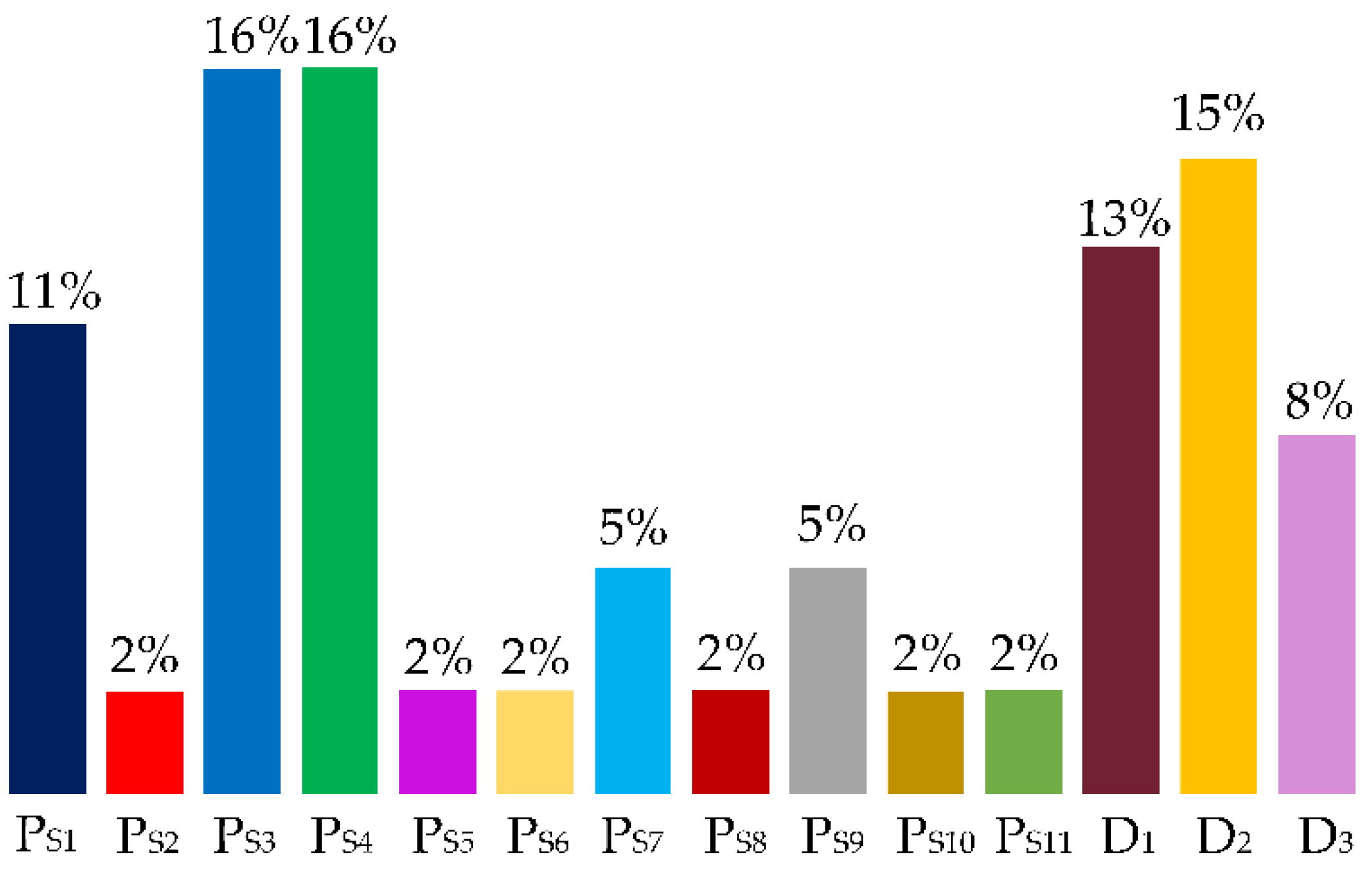
5. Power Loss Analysis

This section discusses the proposed topology’s conduction and switching power losses [34]. This aim is achieved using the current grid value  I o i  during its ith voltage level. Based on this, the RMS value of the grid current  I o 1  in the first voltage level (Zone-I) is calculated as
I o 1 = 1 ω t 1 0 ω t 1 I g , p k 2 sin 2 ( ω t )   d ( ω t ) = I g , p k 2 ω t 1 sin ( 2 ω t 1 ) 4 ω t 1
Additionally, the RMS value of the grid current  I o 2 , I o 3  in the second and third voltage levels (Zone-II and Zone-III) is calculated as
I o 2 = 1 ω t 2 ω t 1 ω t 1 ω t 2 I g , p k 2 sin 2 ( ω t )   d ( ω t ) = I g , p k 1 ω t 2 ω t 1 × 1 2 ω t 2 ω t 1 + 1 4 sin ( 2 ω t 2 ) sin ( 2 ω t 1 )
I o 3 = 1 π ω t 2 ω t 2 ω t 2 π ω t 2 I g , p k 2 sin 2 ( ω t )   d ( ω t ) = I g , p k 1 π 2 ω t 2 × π 2 ω t 2 + sin ( 2 ω t 2 ) 2
where  t 1 = 1 ω sin 1 V i n v g , p k   and   t 2 = 1 ω sin 1 2 V i n v g , p k .

5.1. During the Time Interval  ( 0 , ω t 1 )

The power loss of switch S10 can be calculated as follows:
i S 10 ( 0 , ω t 1 ) = I o 1 ; 0 t d 1 T s   0 ;   d 1 T s t 0
From Equation (35), the RMS value of the switch current  i S 10 , R M S  is calculated as
i S 10 , R M S = I o 1 ω t 1 × d 1 π
By using the above Equation (34), the conduction loss  P C L , S 10  and switching loss  P S W , S 10  of the switch  S 10  is calculated as follows:
P C L , S 10 ( 0 , ω t 1 ) = R n S 10 × i S 10 , R M S ( 0 , ω t 1 ) 2 = R n S 10 × I o 1 2 ω t 1 × d 1 π
P S W , S 10 ( 0 , ω t 1 ) = 1 6 V S 10 × I S 10 × t o n + t o f f × 2 N S W 1 × f g

5.2. During the Time Interval  ( ω t 1 , ω t 2 )

As the switch  S 10  remains ON throughout this time interval, no switching losses are incurred; therefore, only conduction losses are present. Here, the current equation  i S 10 ( ω t , ω t 2 )  is written as
i S 10 ( ω t 1 , ω t 2 ) = I o 2 ; 0 t d 2 T s I o 2 ; d 2 T s t d 2
From Equation (35), the RMS value of the switch current  i S 10 , R M S  in this time interval is calculated as
i S 10 , R M S = I o 2 ω t 2 ω t 1 π
By using the above Equation (37), the conduction loss  P C L , S 10  of the switch  S 10  in this interval is calculated as follows:
P C L , S 10 ( ω t 1 , ω t 2 ) = R n S 10 × i S 10 , R M S ( ω t 1 , ω t 2 ) 2 = R n S 10 × I o 2 2 ω t 2 ω t 1 π

5.3. During the Time Interval  ( ω t 2 , π 2 )

As the switch  S 10  continues to operate, i.e., ON during this time interval, no switching losses are incurred; therefore, only conduction losses are present. Here, the current equation  i S 10 ( ω t , π 2 )  is written as
i S 10 ( ω t , π 2 ) = I o 3 ; 0 t d 3 T s I o 3 ; d 3 T s t d 3
From Equation (35), the RMS value of the switch current  i S 10 , R M S  in this time interval is calculated as
i S 10 , R M S = I o 2 π 2 ω t 2 2 π
By using the above Equation (43), the conduction loss  P C L , S 10  of the switch  S 10  in this interval is calculated as follows:
P C L , S 10 ( ω t 2 , π / 2 ) = R n S 10 × i S 10 , R M S ω t 2 , π / 2 2 = R n S 10 × I o 3 2 π 2 ω t 2 2 π
The total power loss of the switch  S 10  is obtained as (35)–(44):
P S 10 = P C L , S 10 ( 0 , ω t 1 ) + P C L , S 10 ( ω t 1 , ω t 2 ) + P C L , S 10 ( ω t 2 , π / 2 ) + P S W , S 10 ( 0 , ω t 1 )
In the same way, the conduction and switching losses of the remaining semiconductor switches and diodes can be calculated. Using thermal modeling in PLECS/MATLAB-based simulation software, the power loss distribution of the employed semiconductor devices for various operating powers is calculated and shown in Table 3. The switch model IKW30N60DTP and a constant ambient temperature of 25 °C with a uniform temperature distribution across the heatsink were used to calculate the power losses. Figure 6 depicts the bar chart of the power loss distribution percentage of the semiconductors in the proposed topology at rated power. It can be seen that the power loss of switches S3 and S4 in the capacitor charging path is higher due to their parallel path with the source.

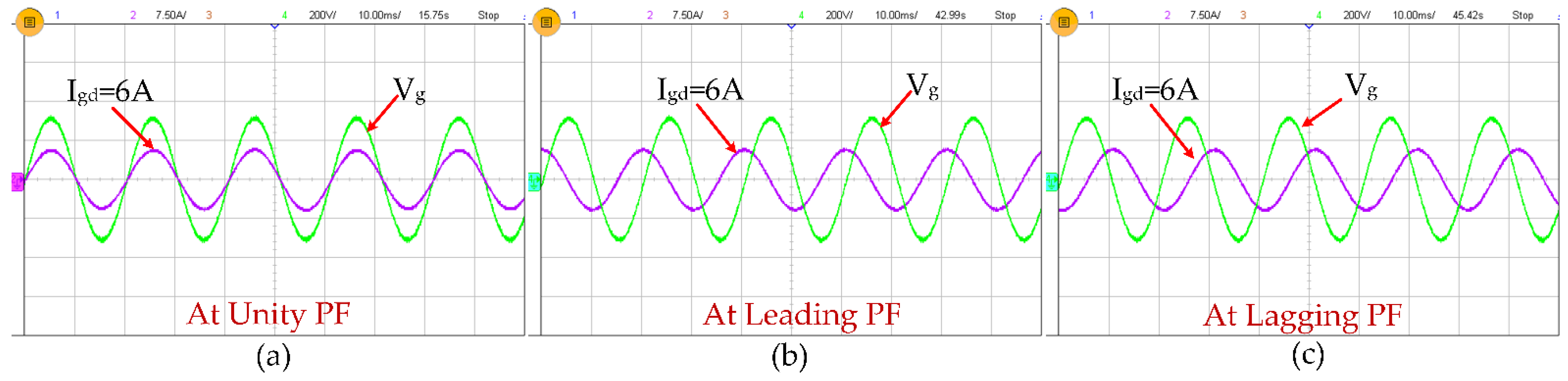
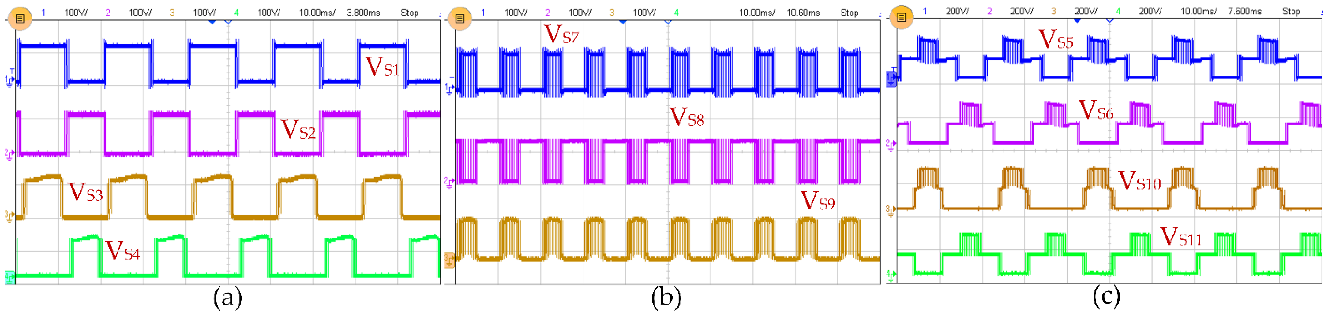
6. Result and Discussion

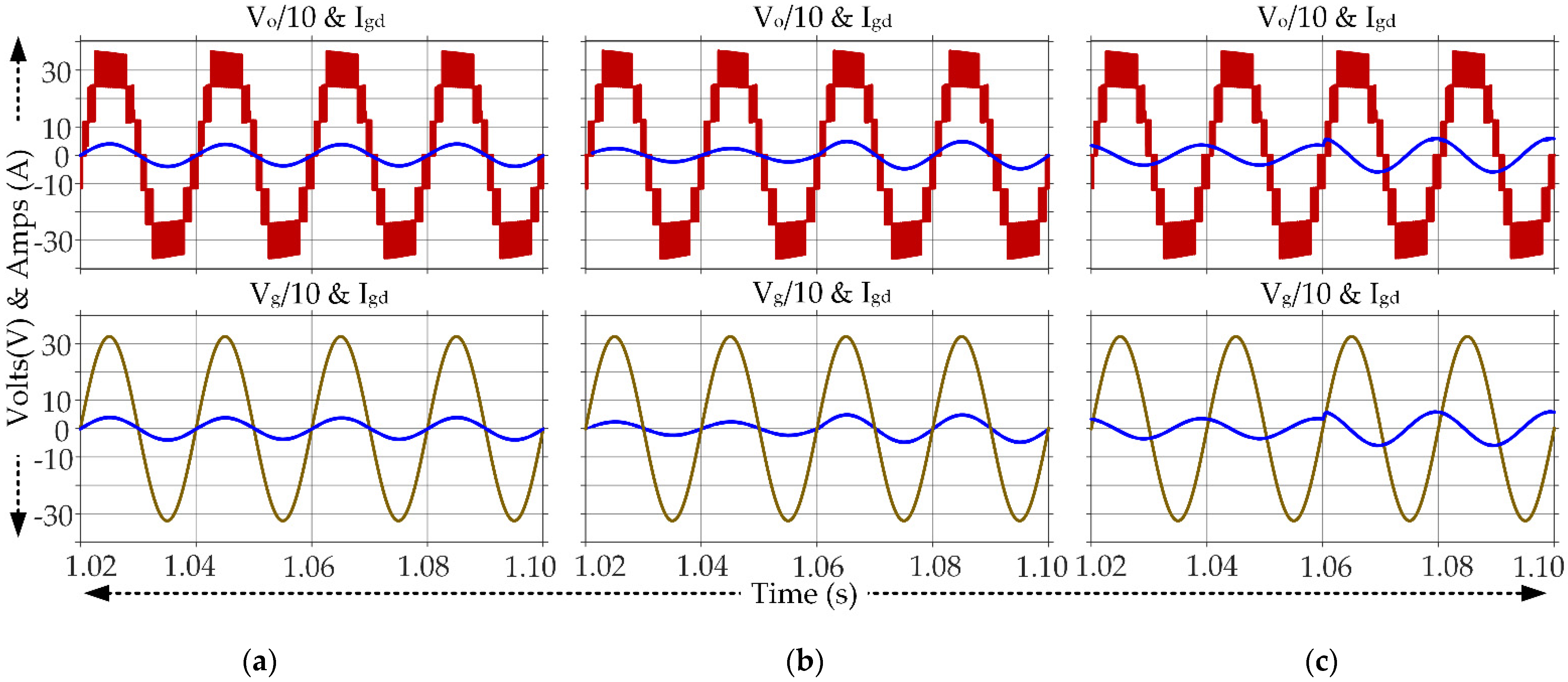
6.1. Simulation Results

The proposed structure is simulated using MATLAB/Simulink environment, and the performance is verified. Here, the input voltage of 125 V is connected into a 220 V (RMS) and 50 Hz grid power system. The proposed inverter generates a seven-level output voltage waveform of 375 V in steps of 125 V, as shown in Figure 7. Additionally, it verifies the boosting ability of the proposed structure. All voltage waveforms in the simulation results are scaled down by 0.1. The performance of 7LCG-TL under grid-connected mode is seen in Figure 7a. It is seen that the maximum value of the injected grid current is 4 A, and the corresponding injected power is 625 W at the unity power factor. When the magnitude of reference current (iref) is changed, a variation of grid current is seen from 3 A to 6 A as shown in Figure 7b. At this unity power factor operating condition, the respective injected power to the grid is 465 W to 935 W. Similarly, the results of a step change in the reactive power mode are illustrated in Figure 7b. It is noticed that, while changing the magnitude of the reference current, the injected power varies from 625 VA to 935 VA. Furthermore, to test the proposed inverter’s performance under varying input voltage conditions, the input voltage is varied from 105 V to 125 V. The respective inverter output voltage, grid voltage, and grid current waveforms at 935 W unity power factor are shown in Figure 8b–d. The inverter output voltage and grid voltage waveforms are scaled down by 0.1. From Figure 8b, it is observed that the inverter output voltage changes from 315 V to 375 V while changing the input from 105 V to 125 V. However, the grid voltage and current remain the same for the 935 W unity power factor. The leakage current suppression capability of the proposed 7LCG-TL topology is tested at 935 W injected power as shown in Figure 9. Here, a 75-nF capacitor has been utilized to figure out the effect of CPV and the obtained maximum RMS value of leakage current (ileak) is around 8.5 mA.

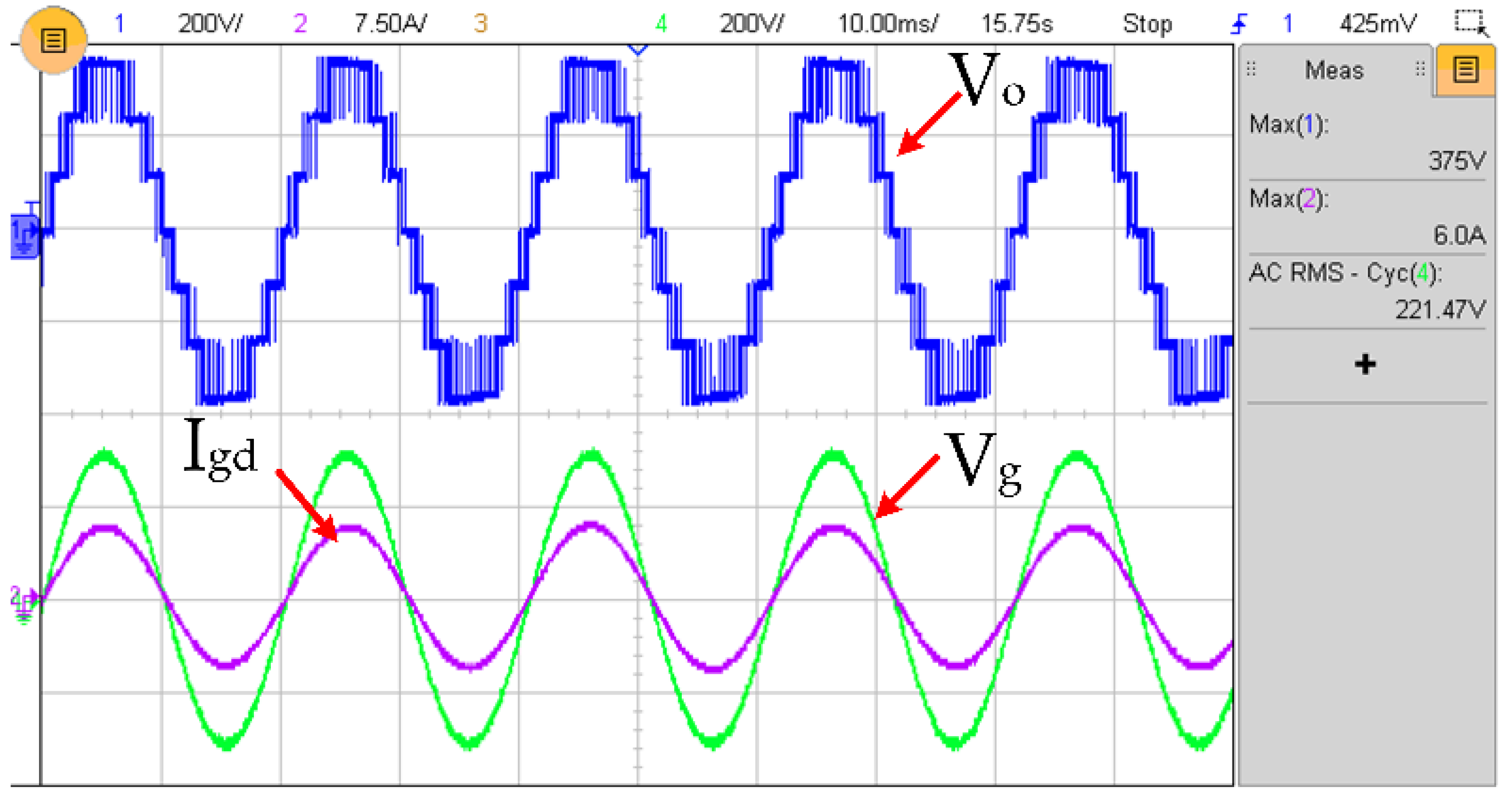
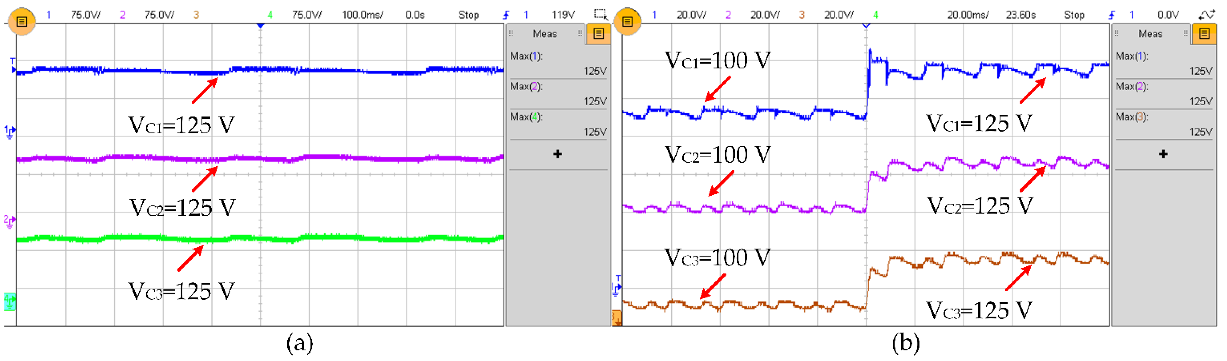
6.2. Experimental Results

The performance of the proposed topology is validated experimentally using a 935 W laboratory setup. The details of the components and their specifications used for the laboratory prototype are given in Table 4. Here, an input voltage of 125 V is applied to generate a seven-level peak output voltage of magnitude 375 V. Figure 10 shows the waveforms of the seven-level inverter output voltage, the gird-voltage, and the injected grid-current. It can be seen that the peak value of the inverter’s output voltage is 375 V and the peak value of the injected grid current is 6 A at unity power factor.
Figure 11a,b shows the voltage across capacitors C1, C2, and C3 when the input is set to 125 V and when it is changed from 100 V to 125 V. From Figure 11a,b, it is clear that the capacitor voltages are well balanced at the source voltage without any extra control circuits. Furthermore, the operability of the proposed topology under different power factor conditions such as unity, leading, and lagging is verified, and the corresponding grid-voltage and injected grid-current waveforms are shown in Figure 12a–c. Figure 13a–c shows the different values of power 465 W, 700 W, and 780 W injected into the grid. The grid current value is changed from 3 A to 6 A when the step change in magnitude of reference current (iref) is applied, verifying the dynamic operating characteristic of the proposed structure. As seen in Figure 14, the injected grid power varies between 465 W and 935 W during these dynamic variation conditions. During experimentation, a small inductor of 40 uH is inserted in the capacitor charging loop to reduce the high inrush current. The voltage stress of power semiconductor switches is shown in Figure 15a–c. According to Figure 15a–c, the maximum voltage stress for switches S1–S4 and S7–S9 equals the source voltage, whereas switches S5, S6, S10, and S11 are subjected to double the source voltage. Figure 16 shows the efficiency graph between experimental versus simulation at a unity power factor condition. The simulation efficiency is 97.85%, with a total loss of 12 W for ~545 W of output power. However, in the experimental setup, the efficiency is ~97.18% for the unity pf, as depicted in Figure 16.

7. Comparative Study

A comprehensive comparison of the proposed structure against recent seven-level inverter structures has been performed and is provided in Table 5. The comparison is performed based on features such as the number of power semiconductor devices, total standing voltage per unit, boosting ability, maximum blocking voltage, leakage current alleviation, and efficiency. As seen from Table 5, it is clear that the topologies [35,36] use a lower number of devices than the proposed topology to generate the triple voltage gain. However, they require four higher rating switches due to the utilization of the H-bridge structure at their back-end. The topologies [37,38,39,40,41,42,43] also use lower power components than the proposed inverter, but their voltage gain is only 1.5. Additionally, the total standing voltage of the proposed structure is 5, which is the lowest value in the comparison study. The MBV of the proposed structure is 2Vin, which is the second lowest in the comparison table. Even though the proposed topology and topology [44] both have the same number of power components, [44] has a higher peak inverse voltage, so the ratio of MBV to maximum output voltage is also high. For the same seven-level triple voltage gain, the topology [45] uses a higher number of components than the proposed structure, and their TSV, MBV, and ratio of MBV to maximum output voltage are also high. The MBV and TSV of the topology [46] is higher than the proposed topology. Similar to the proposed topology, the topologies presented in [47,48] are also of the common ground-type structure where the neutral terminal of the grid is directly connected to the negative terminal of the DC source. Due to this structure, the leakage current can be alleviated. This feature is absent in all other topologies listed in Table 5. Though the topology [47] offers a common ground feature similar to the proposed topology, they use three capacitors, out of which two capacitors are of the voltage rating Vin and the rating of the third capacitor is 2Vin, whereas the proposed topology uses three capacitors of the same voltage rating Vin.
By keeping the duty cycle of the switch S1 of the structure presented in [48] at 50%, it will generate an output voltage with a voltage gain of 2. Still, the MBV is equal to the output voltage. So, even if the duty cycle changes to increase the boosting factor, 5 out of 10 switches have to withstand voltage equal to the output voltage.

8. Conclusions

This article presents a novel 7L transformerless inverter topology with a common ground feature and voltage boosting. The common ground-type structure ensures the elimination of leakage current. The proposed topology uses three switched capacitors of the same voltage rating, i.e., equal to the input, to generate the triple boost output voltage. Additionally, the capacitors are balanced without any additional control requirements. The obtained experimental results prove that the voltages across all the switches were lower than the maximum output voltage, avoiding the use of high-voltage semiconductor devices. The ability to handle reactive power with the grid’s lagging/leading pf condition is verified from the experimental results. The RMS value of the leakage current is 8 mA for the proposed topology, which verifies its leakage current suppression capability. Furthermore, the design of passive components and power loss analysis have been presented. The outcome of a comprehensive comparison against other 7L topologies has been presented to show the merits of the proposed structure. Furthermore, to validate the performance of the proposed structure, experimental results were obtained from a 935 W laboratory prototype. Both simulation and experimental results are in good agreement, confirming the feasibility of the proposed topology. At ~935 W, 96.5% is the efficiency value while using PLECS simulation software, and 95.8% is an experimental value. Given the benefits highlighted in this study, the proposed structure is a strong candidate for grid-connected PV applications.

Author Contributions

Conceptualization, N.P.G., K.V. and J.S.M.A.; methodology, N.P.G., K.V. and J.S.M.A.; software, N.P.G. and S.S.; validation, K.V. and J.S.M.A.; formal analysis, K.V.; investigation, K.V. and J.S.M.A.; resources, K.V., J.S.M.A. and K.R.; data curation, J.S.M.A. and S.S.; writing—original draft preparation, N.P.G. and S.S.; writing—review and editing, K.V., J.S.M.A. and K.R.; supervision, K.V.; project administration, K.V. and J.S.M.A. All authors have read and agreed to the published version of the manuscript.

Funding

This research received no external funding.

Data Availability Statement

All data generated or analyzed during this study are included in this article.

Acknowledgments

The authors would like to acknowledge the support of Prince Sultan University for paying the Article Processing Charges (APC) of this publication.

Conflicts of Interest

The authors declare no conflict of interest.

Nomenclature

CGCommon Groundis (1,2,3…11)Current stress of switches S1,2,3…11
GC-PVGrid-connected photo voltaic systemd1, d2, and d3Duty cycle for the operation Zones I, II and III
SCSwitched Capacitor   V o , m x Maximum value of the inverter output voltage
7LCG-TLSeven-Level Common Ground-Transformerless   i L f ,   V C Inductor current and capacitor voltage ripple
C1, C2 and C3CapacitorsMBVMaximum blocking voltage
VC1, VC2, VC3Voltage across capacitors C1, C2 and C3TSVTotal standing voltage
Vin, and VoInput and Output voltage LDCLongest discharge period
  v g ( t ) , i g d ( t ) Grid voltage and current   P C L , S 10 ,   P S W , S 10 Conduction and switching loss of switch S10
  V g , p k ,   I g , p k Peak value of grid voltage and current   i S 10 , R M S RMS value of the switch current
  I o 1 ( o 2 , o 3 ) RMS value of grid current in Zone I, II and III   P S ( 1 , 2 , 11 ) Power loss of switches S(1,1…11)
  I c h a r , C 1 ( C 2 , C 3 ) Capacitor charging current of C1, C2 and C3. L f Filter inductor

References

  1. Subramaniam, U.; Bhaskar, S.M.; Almakhles, D.J.; Padmanaban, S.; Leonowicz, Z. Investigations on EMI Mitigation Techniques: Intent to Reduce Grid-Tied PV Inverter Common Mode Current and Voltage. Energies 2019, 12, 3395. [Google Scholar] [CrossRef] [Green Version]
  2. Bayrak, G.; Ghaderi, D.; Subramaniam, U. Leakage current repression and real-time spectrum analysis with chirp Z-transform for a novel high-efficiency PV-based inverter applicable in micro-grids. Electr. Eng. 2020, 102, 2041–2057. [Google Scholar] [CrossRef]
  3. Sunddararaj, S.P.; Rangarajan, S.S.; Nallusamy, S.; Subramaniam, U.; Collins, E.R.; Senjyu, T. Design of Novel HG-SIQBC-Fed Multilevel Inverter for Standalone Microgrid Applications. Appl. Sci. 2022, 12, 9347. [Google Scholar] [CrossRef]
  4. Ghoudelbourk, S.; Azar, A.T.; Dib, D.; Omeiri, A. Selectivee harmonic elimination strategy in the multilevel inverters for grid connected photovoltaic system. Int. J. Adv. Intell. Paradig. 2020, 15, 317–339. [Google Scholar] [CrossRef]
  5. Sandeep, N.; Sathik, M.J.; Yaragatti, U.R.; Krishnasamy, V.; Verma, A.K.; Pota, H.R. Common-Ground-Type Five-Level Transformerless Inverter Topology with Full DC-Bus Utilization. IEEE Trans. Ind. Appl. 2020, 56, 4071–4080. [Google Scholar] [CrossRef]
  6. Gubía, E.; Sanchis, P.; Ursúa, A.; López, J.; Marroyo, L. Ground currents in single-phase transformerless photovoltaic systems. Prog. Photovolt Res. Appl. 2007, 15, 629–650. [Google Scholar] [CrossRef]
  7. Duong, T.D.; Nguyen, M.K.; Tran, T.T.; Vo, D.V.; Lim, Y.C.; Choi, J.H. Topology Review of Three-Phase Two-Level Transformerless Photovoltaic Inverters for Common-Mode Voltage Reduction. Energies 2022, 15, 3106. [Google Scholar] [CrossRef]
  8. Vosoughi Kurdkandi, N.; Ghavipanjeh Marangalu, M.; Husev, O.; Aghaie, A.; Islam, M.R.; Siwakoti, Y.; Muttaqi, K.; Hosseini, S.H. A New Seven-Level Transformer-Less Grid-Tied Inverter with Leakage Current Limitation and Voltage Boosting Feature. IEEE J. Emerg. Sel. Top. Ind. Electron. 2022, 4, 228–241. [Google Scholar] [CrossRef]
  9. Kibria, M.F.; Elsanabary, A.; Tey, K.S.; Mubin, M.; Mekhilef, S. A Comparative Review on Single Phase Transformerless Inverter Topologies for Grid-Connected Photovoltaic Systems. Energies 2023, 16, 1363. [Google Scholar] [CrossRef]
  10. Das, C.K.; Annamalai, K.; Tirumala, S.V. A Quasi Z-Source Based Five-Level PV Inverter with Leakage Current Reduction. IEEE Trans. Ind. Appl. 2021, 58, 400–412. [Google Scholar] [CrossRef]
  11. Mishra, S.; Adda, R.; Joshi, A. Inverse Watkins–Johnson Topology-Based Inverter. IEEE Trans. Power Electron. 2012, 27, 1066–1070. [Google Scholar] [CrossRef]
  12. Nguyen, M.-K.; Le, T.-V.; Park, S.-J.; Lim, Y.-C. A Class of Quasi-Switched Boost Inverters. IEEE Trans. Ind. Electron. 2015, 62, 1526–1536. [Google Scholar] [CrossRef]
  13. Barath, J.N.; Soundarrajan, A.; Stepenko, S.; Husev, O.; Vinnikov, D.; Nguyen, M.-K. Topological Review of Quasi-Switched Boost Inverters. Electronics 2021, 10, 1485. [Google Scholar] [CrossRef]
  14. Gaafar, M.A.; Orabi, M.; Ibrahim, A.; Kennel, R.; Abdelrahem, M. Common-Ground Photovoltaic Inverters for Leakage Current Mitigation: Comparative Review. Appl. Sci. 2021, 11, 11266. [Google Scholar] [CrossRef]
  15. Jahan, H.K.; Kurdkandi, N.V.; Abapour, M.; Zare, K.; Hosseini, S.H.; Yang, Y.; Blaabjerg, F. Common-Ground-Type Single-Source High Step-up Cascaded Multilevel Inverter for Transformerless PV Applications. Mathematics 2020, 8, 1716. [Google Scholar] [CrossRef]
  16. Siwakoti, Y.P.; Blaabjerg, F. Common-Ground-Type Transformerless Inverters for Single-Phase Solar Photovoltaic Systems. IEEE Trans. Ind. Electron. 2018, 65, 2100–2111. [Google Scholar] [CrossRef]
  17. Ardashir, J.F.; Sabahi, M.; Hosseini, S.H.; Blaabjerg, F.; Babaei, E.; Gharehpetian, G.B. A Single-Phase Transformerless Inverter with Charge Pump Circuit Concept for Grid-Tied PV Applications. IEEE Trans. Ind. Electron. 2017, 64, 5403–5415. [Google Scholar] [CrossRef]
  18. Grigoletto, F.B. Five-Level Transformerless Inverter for Single-Phase Solar Photovoltaic Applications. IEEE J. Emerg. Sel. Top. Power Electron. 2020, 8, 3411–3422. [Google Scholar] [CrossRef]
  19. Grigoletto, F.B. Multilevel Common-Ground Transformerless Inverter for Photovoltaic Applications. IEEE J. Emerg. Sel. Top. Power Electron. 2021, 9, 831–842. [Google Scholar] [CrossRef]
  20. Kadam, A.; Shukla, A. A Multilevel Transformerless Inverter Employing Ground Connection Between PV Negative Terminal and Grid Neutral Point. IEEE Trans. Ind. Electron. 2017, 64, 8897–8907. [Google Scholar] [CrossRef]
  21. Pandurengan, G.N.; Krishnasamy, V.; Mohamed, J.S.; Almakhles, D.; Engineering, E.; Nadu, T.; Arabia, S.; Nadu, T.; Arabia, S. Five-Level Transformerless Common Ground Type Inverter with Reduced Device Count. Inf. MIDEM-J. Microelectron. Electron. Compon. Mater. 2022, 51, 71–82. [Google Scholar] [CrossRef]
  22. Vosoughi, N.; Hosseini, S.H.; Sabahi, M. A New Transformer-Less Five-Level Grid-Tied Inverter for Photovoltaic Applications. IEEE Trans. Energy Convers. 2020, 35, 106–118. [Google Scholar] [CrossRef]
  23. Anand, V.; Singh, V.; Ali, J.S.M. Dual Boost Five-Level Switched-Capacitor Inverter with Common Ground. IEEE Trans. Circuits Syst. II Express Briefs 2023, 70, 556–560. [Google Scholar] [CrossRef]
  24. Kumari, S.; Verma, A.; Sandeep, N.; Yaragatti, U.; Pota, H. A Five-Level Transformer-Less Inverter with Self-Voltage Balancing and Boosting Ability. IEEE Trans. Ind. Appl. 2021, 57, 6237–6245. [Google Scholar] [CrossRef]
  25. Kumari, S.; Verma, A.K.; Sandeep, N.; Yaragatti, U.R.; Pota, H.R. Multilevel common-ground inverter with voltage boosting for PV applications. IET Power Electron. 2021, 14, 901–911. [Google Scholar] [CrossRef]
  26. Kumari, S.; Sandeep, N.; Verma, A.; Yaragatti, U.R.; Pota, H. Design and Implementation of Transformer-Less Common-Ground Inverter With Reduced Components. IEEE Trans. Ind. Appl. 2022, 9994, 1–10. [Google Scholar] [CrossRef]
  27. Marangalu, M.G.; Hosseini, S.H.; Kurdkandi, N.V.; Khoshkbar-Sadigh, A. A New Five-Level Switched-Capacitor-Based Transformer-Less Common-Grounded Grid-Tied Inverter. IEEE J. Emerg. Sel. Top. Power Electron. 2022. [Google Scholar] [CrossRef]
  28. Sathik, M.J.; Almakhles, D.J. Common Ground Type Five Level Inverter with Voltage Boosting for PV Applications. Sci. Rep. 2022, 12, 2–11. [Google Scholar] [CrossRef]
  29. Mohamed Ali, J.S.; Hota, A.; Sandeep, N.; Almakhles, D.J. A Single-Stage Common Ground-Type Transformerless Five-Level Inverter Topology. IEEE J. Emerg. Sel. Top. Power Electron. 2022, 10, 837–845. [Google Scholar] [CrossRef]
  30. Barzegarkhoo, R.; Farhangi, M.; Aguilera, R.P.; Lee, S.S.; Blaabjerg, F.; Siwakoti, Y.P. Common-Ground Grid-Connected Five-Level Transformerless Inverter With Integrated Dynamic Voltage Boosting Feature. IEEE J. Emerg. Sel. Top. Power Electron. 2022, 10, 6661–6672. [Google Scholar] [CrossRef]
  31. Almakhles, D.J.; Sathik, M.J. Single—Phase Transformerless Nine—Level Inverter with Voltage Boosting Ability for PV Fed AC Microgrid Applications. Sci. Rep. 2022, 12, 13442. [Google Scholar] [CrossRef]
  32. Gopinath, N.P.; Vijayakumar, K. Common Ground Nine-Level Boost Inverter for Grid-Connected PV Applications. Front. Energy Res. 2022, 10, 922786. [Google Scholar] [CrossRef]
  33. Chen, M.; Yang, Y.; Loh, P.C.; Blaabjerg, F. A Single-Source Nine-Level Boost Inverter with a Low Switch Count. IEEE Trans. Ind. Electron. 2022, 69, 2644–2658. [Google Scholar] [CrossRef]
  34. Kurdkandi, N.V.; Marangalu, M.G.; Mohammadsalehian, S.; Tarzamni, H.; Siwakoti, Y.P.; Islam, M.R.; Muttaqi, K.M. A New Six-Level Transformer-Less Grid-Connected Solar Photovoltaic Inverter with Less Leakage Current. IEEE Access 2022, 10, 63736–63753. [Google Scholar] [CrossRef]
  35. Chen, J.; Wang, C.; Li, J. A Single-Phase Step-Up Seven-Level Inverter with a Simple Implementation Method for Level-Shifted Modulation Schemes. IEEE Access 2019, 7, 146552–146565. [Google Scholar] [CrossRef]
  36. Shahsavar, T.H.; Babaei, E.; Sabahi, M.; khoshkbar-Sadigh, A. A New Boost Type Single Source Seven-Level Switched-Capacitor Based Inverter with Reduced Current Stress over the Components. Comput. Electr. Eng. 2022, 101, 108160. [Google Scholar] [CrossRef]
  37. Liu, J.; Zhu, X.; Zeng, J. A Seven-Level Inverter With Self-Balancing and Low-Voltage Stress. IEEE J. Emerg. Sel. Top. Power Electron. 2020, 8, 685–696. [Google Scholar] [CrossRef]
  38. Lee, S.S.; Member, S.; Lee, K.; Member, S. Dual-T-Type Seven-Level Boost Active-Neutral-Point-Clamped Inverter. IEEE Trans. Power Electron. 2019, 34, 6031–6035. [Google Scholar] [CrossRef]
  39. Sathik, M.J.; Sandeep, N.; Blaabjerg, F. High Gain Active Neutral Point Clamped Seven-Level Self-Voltage Balancing Inverter. IEEE Trans. Circuits Syst. II Express Briefs 2020, 67, 2567–2571. [Google Scholar] [CrossRef]
  40. Kakar, S.; Arif, M.; Ayob, S.M.; Nordin, N.; Mekhilef, S.; Seyedmahmoudian, M.; Stojcevski, A. An Improved Seven-Level Switched-Capacitor-Based Neutral-Point Clamped Inverter. Front. Energy Res. 2022, 10, 1–10. [Google Scholar] [CrossRef]
  41. Zhao, J.; Chen, Y.; Zeng, J.; Liu, J. Low-Voltage Stress Seven-Level Inverter Based on Symmetrical Capacitors. IEEE J. Emerg. Sel. Top. Power Electron. 2022, 10, 3033–3044. [Google Scholar] [CrossRef]
  42. Agarwal, R.; Gupta, K.K.; Singh, S. Switched capacitors-based single-phase seven-level photovoltaic inverter with self-voltage balancing. Electr. Eng. 2022, 104, 3107–3117. [Google Scholar] [CrossRef]
  43. Gao, Y.; Zhang, W.; Naderi Zarnaghi, Y.; Vosoughi Kurdkandi, N.; Zhang, C. A New Boost Switched Capacitor Seven-Level Grid-Tied Inverter. IET Power Electron. 2021, 14, 268–279. [Google Scholar] [CrossRef]
  44. He, L.; Sun, J.; Lin, Z.; Cheng, B. Capacitor-Voltage Self-Balance Seven-Level Inverter with Unequal Amplitude Carrier-Based APODPWM. IEEE Trans. Power Electron. 2021, 36, 14002–14013. [Google Scholar] [CrossRef]
  45. Chen, M. Novel Cascaded Seven-Level Inverter With Embedded Voltage Boosting for Renewable Energy Applications. CPSS Trans. Power Electron. Appl. 2022, 7, 58–70. [Google Scholar] [CrossRef]
  46. Roy, T.; Tesfay, M.W.; Nayak, B.; Panigrahi, C.K. A 7-Level Switched Capacitor Multilevel Inverter with Reduced Switches and Voltage Stresses. IEEE Trans. Circuits Syst. II Express Briefs 2021, 68, 3587–3591. [Google Scholar] [CrossRef]
  47. Grigoletto, F.B.; de Vilhena Moura, P.H.; Chaves, D.B.; Vilaverde, J.D.S. Step-Up Seven-Level Common-Ground Transformerless Inverter. In Proceedings of the 2021 14th IEEE International Conference on Industry Applications (INDUSCON), São Paulo, Brazil, 15–18 August 2021; pp. 716–722. [Google Scholar] [CrossRef]
  48. Barzegarkhoo, R.; Farhangi, M.; Lee, S.S.; Aguilera, R.P.; Siwakoti, Y.P. A Novel Seven-Level Switched-Boost Common-Ground Inverter with Single-Stage Dynamic Voltage Boosting Gain. In Proceedings of the 2022 International Power Electronics Conference (IPEC-Himeji 2022- ECCE Asia), Himeji, Japan, 15–19 May 2022; pp. 873–877. [Google Scholar] [CrossRef]
  49. Siddique, M.D.; Mekhilef, S.; Mekhilef, S.; Shah, N.M.; Ali, J.S.M.; Blaabjerg, F. A New Switched Capacitor 7L Inverter with Triple Voltage Gain and Low Voltage Stress. IEEE Trans. Circuits Syst. II Express Briefs 2020, 67, 1294–1298. [Google Scholar] [CrossRef]
Figure 1. Grid-tied common ground transformerless inverter with leakage current path.
Energies 16 03428 g001
Figure 2. Proposed 7LCG-TL topology.
Energies 16 03428 g002
Figure 3. Conductive path of output voltage levels (a) +3Vin, (b) +2Vin, (c) +Vin, (d) 0, (e) −Vin, (f) −2Vin, and (g) −3Vin.
Energies 16 03428 g003
Figure 4. (a) Generalized common mode circuit of a transformerless inverter; (b) proposed common ground-type topology.
Energies 16 03428 g004
Figure 5. The inverter output voltage, grid voltage, and operating zones of the proposed inverter.
Energies 16 03428 g005
Figure 6. PLECS loss analysis at rated power and 20 kHz fixed switching frequency.
Energies 16 03428 g006
Figure 7. MATLAB results of the: (a) inverter’s voltage, grid voltage, and injected grid current, (b) inverter’s voltage, grid voltage, and injected current when variation in reference current is applied at unity pf, and (c) inverter’s voltage, grid voltage, and injected grid current when the change in reference current is applied at leading pf.
Energies 16 03428 g007
Figure 8. Response when input voltage change is applied, (a) input change from 105 V to 125 V, (b) inverter output voltage, (c) grid voltage, and (d) grid current.
Energies 16 03428 g008
Figure 9. Leakage current waveform.
Energies 16 03428 g009
Figure 10. Experimental result of inverter’s voltage, grid voltage, and injected grid-current at unity power factor.
Energies 16 03428 g010
Figure 11. Experimental result of (a) capacitor voltages VC1, VC2, and VC3 and (b) capacitor voltages VC1, VC2, and VC3 when step input change is applied.
Energies 16 03428 g011
Figure 12. Experimental result of grid voltage and injected grid-current at different pf: (a) unity, (b) leading, and (c) lagging.
Energies 16 03428 g012
Figure 13. Experimental result of grid voltage and injected grid-current at (a) 465 W output power, (b) 700 W output power, and (c) 780 W output power.
Energies 16 03428 g013
Figure 14. Experimental result of inverter’s voltage, grid voltage, and injected grid-current when change of reference current is applied.
Energies 16 03428 g014
Figure 15. Voltage stress across the switches (a) Switch S1–S4, (b) Switch S7–S9 and (c) S5, S6, S10, and S11.
Energies 16 03428 g015
Figure 16. Efficiency at unity power factor.
Energies 16 03428 g016
Table 1. Switching sequence.
LevelStatus of SwitchesStatus of
Capacitors
Output
Voltage
S1S2S3S4S5S6S7S8S9S10S11C1C2C3
+310101001010CDD+3Vin
+210101010010CD-+2Vin
+110110010110CCC+1Vin
010110010101CCC0
−110010110001CD-−Vin
−201010100101D-D−2Vin
−301010101001DDD−3Vin
Table 2. Voltage stress of switches.
Voltage
Level
Voltage Stress of Switches
S1S2S3S4S5S6S7S8S9S10S11
+30   V i n 0   V i n 0   2 V i n   V i n 0   V i n 0   2 V i n
+20   V i n 0   V i n 0   V i n 0   V i n 00   V i n
+10   V i n 00   V i n   V i n 0   V i n 00   V i n
00   V i n 00   V i n   V i n 0   V i n 0   V i n 0
−10   V i n   V i n 0   V i n 00   V i n 0   V i n 0
−2   V i n 0   V i n 0   V i n 00   V i n 0   V i n 0
−3   V i n 0   V i n 0   2 V i n 0   V i n 0   V i n   2 V i n 0
Table 3. The power loss of semiconductor devices of the proposed topology.
Output Power (W)PS1PS2PS3PS4PS5PS6PS7PS8PS9PS10PS11PD1PD2PD3
5451.3000.2801.7851.7940.1930.2290.6010.2490.5990.3000.1941.5651.8831.027
6251.8810.3802.7242.7270.2740.3150.8950.3520.8950.3930.2742.4842.9441.460
7802.6690.5584.0263.9960.3820.4471.2810.4841.2810.5850.3793.1703.6892.054
9353.7280.8155.7545.6620.5300.6351.7950.6631.7920.8700.5224.3405.0452.850
Table 4. Experimental specifications.
DeviceSpecification
IGBT switchesSKM75GB063D, 600 V/75 A
Capacitors C1, C2, and C3SAMWHA HK, 1000 uF/450 V
Diodes D1, D2, and D3RHRG3060-F085, 600 V/30 A
Inductor LfFerrite core, 2.6 mH
Gate DriverTLP250-IC
Digital ControllerTMS320F28379D
Input Voltage (Vin)125 V
Output Voltage (Vo)375 V
Output power (W)935 W
Grid Voltage220 V (RMS)
Switching Frequency20 kHz
Local Grid Frequency50 Hz
Table 5. Comparative study against recent 7L topologies.
TopologyABCDFGHIJKLMN (%)
[37]10803Vin5.31:1.510.67NoYesNoNR
[38]10804Vin7.31:1.521.33NoYesNo[email protected] kW
[39]10903Vin61:1.510.67NoYesNo96@1 kW,
[35]9912Vin5.71:331YesYesNo92.81@150 W
[36]109112Vin7.331:331YesYesNo96.68@210 W
[44]121204Vin5.51:441NoYesNo97.62@200 W
[40]1211440.5Vin81:1.521.33NoYesNo[email protected] kW
[45]1210442Vin7.31:341.33NoYesNo94.9@500 W
[41]108020.5Vin5.31:1.510.67NoYesNo97.6@400 W
[42]99040.5Vin5.31:1.510.67NoYesNoNR
[49]121102Vin5.31:320.67NoYesNo95@1 kW
[46]9923Vin5.7 1:331NoYesNo93.1@313 W
[43]108040.5Vin5.71:1.510.67NoYesNoNR
[47]88432Vin5.31:331NoNoYesNR
[48]101003Vin6.81:221NoNoYesNR
Proposed111133Vin51:320.67NoNoYes96.5@935 W
A—Switch Count, B—Gate Driver Count, C—Diode Count, D—Capacitor Count, E—Maximum No. of. ON Switches, F—Maximum Capacitor Voltage Rating, G—TSV (per unit), H—Boost factor (Vin:Vo), I—MBV (×Vin), J—MBV/Maximum output voltage (should be low), K—H-Bridge, L—Leakage Current, M—CG Structure, N—Efficiency η (%), NR—Not Reported.
Disclaimer/Publisher’s Note: The statements, opinions and data contained in all publications are solely those of the individual author(s) and contributor(s) and not of MDPI and/or the editor(s). MDPI and/or the editor(s) disclaim responsibility for any injury to people or property resulting from any ideas, methods, instructions or products referred to in the content.

