Abstract
This paper investigates the current sink capacitor technique as a method to minimize the turn-off power losses of SiC MOSFETs operated with zero-voltage switching (ZVS). The method is simple and is based on adding auxiliary capacitors in parallel to the transistors, allowing the sink capacitor to take over part of the channel current, thus limiting the power loss while also advantageously lowering the ratio. The technique is validated and experimentally studied based on a single-pulse test setup with 1200 V-rated SiC MOSFETs, with several capacitances and gate resistance values, at various switched currents up to roughly 60 A. It is shown that by employing even very small capacitances, in the range of nanofarads, the turn-off power loss can be reduced by over tenfold, with a negligible impact on the volume and complexity of the system. Thus, the presented method can be effectively employed to improve soft-switched power converters.
1. Introduction
Considering the superior switching performance of SiC MOSFETs compared to their Si counterparts, namely, lower power loss and faster switching speeds, SiC transistors have already been successfully introduced as the power switch of choice in modern power electronics aiming for high efficiency or power density [1,2,3]. When low-volume solutions are regarded, notable operating frequencies, even in the range of hundreds of kHz, need to be employed [4,5]. Thus, even though the switching losses in SiC devices are already relatively low, they are still a limiting factor for constructing highly compact converters. Hence, soft switching concepts are considered, e.g., in the form of zero-voltage switching (ZVS) [6,7]. Nevertheless, these approaches usually limit the turn-on switching loss only, while the turn-off process, even though it exhibits lower losses in general, is still a substantial hindrance for constructing high-power-density power converters [8,9,10], as it may lead to enlarged cooling requirements or lower energy efficiencies.
Achieving soft turn-off in SiC MOSFETs to maximize the switching frequency has been a research target for several years now, and a number of publications have presented analytical models for the turn-off process, which also include the impact of stray inductances on switching behavior [9,11,12,13]. Principally, soft turn-off can be realized via the gate driver [14] or through auxiliary snubber-like circuits in parallel to the switch [15]. The first considered approach is based on the idea that if a specific high current is delivered to the gate during turn-off, the process is largely shortened, and in practice, soft turn-off with minimal power losses is reached [11]. However, as near-short-circuit gate driver currents are required for high-switched MOSFET currents, designing such drivers is a challenging task. Furthermore, this driver behavior leads to extremely fast switching of the SiC device, leading to colossal and ratios. These, combined with circuit parasitics, even if vastly minimized through the careful design of the power circuit, result in significant issues with EMI generation, as well as increased power losses. However, there are solutions that rely on passive components to improve the switch-off performance, either with conventional RC snubbers [15], more advanced active circuits [16], or streamlined circuits with an auxiliary capacitor as the sole addition [17,18].
Taking into account the simplest solution, with the lowest impact on the volume of the system, a current sink capacitor technique employing an auxiliary capacitor in parallel to the SiC device is considered in this paper. Essentially, the extra capacitor sinks the channel current during the turn-off process and leads to notably reduced turn-off power losses, shorter transition times, and reduced transient overvoltages and oscillations [18]; while the concept has already been presented and analyzed in prior studies, it was either considered for a specific application [18], aimed at more complex circuit structures [16], or focused on modeling while lacking experimental validation with regard to the turn-off loss reduction [17]. To this end, in this paper, a thorough experimental study, taking into account several auxiliary capacitance values, is exhibited, validating the current sink capacitor technique as a general method to minimize the turn-off switching losses of zero-voltage-switched (ZVS) transistors. Therefore, the efficiency of the converters can be maximized, and the cooling requirements for the systems may be lowered.
The article is constructed as follows: After a concise introduction, a theoretical investigation of the turn-off process of SiC MOSFETs with the associated power losses is given in Section 2, focusing on the impact of the suggested current sink capacitor technique. Furthermore, a laboratory test setup is exhibited, along with the experimental study validating the suggested concept. Finally, the paper is concluded in Section 4, establishing the proposed method as a simple technique to limit power losses in ZVS-operated power converters.
2. SiC MOSFET Zero Turn-Off Loss Process Phenomena
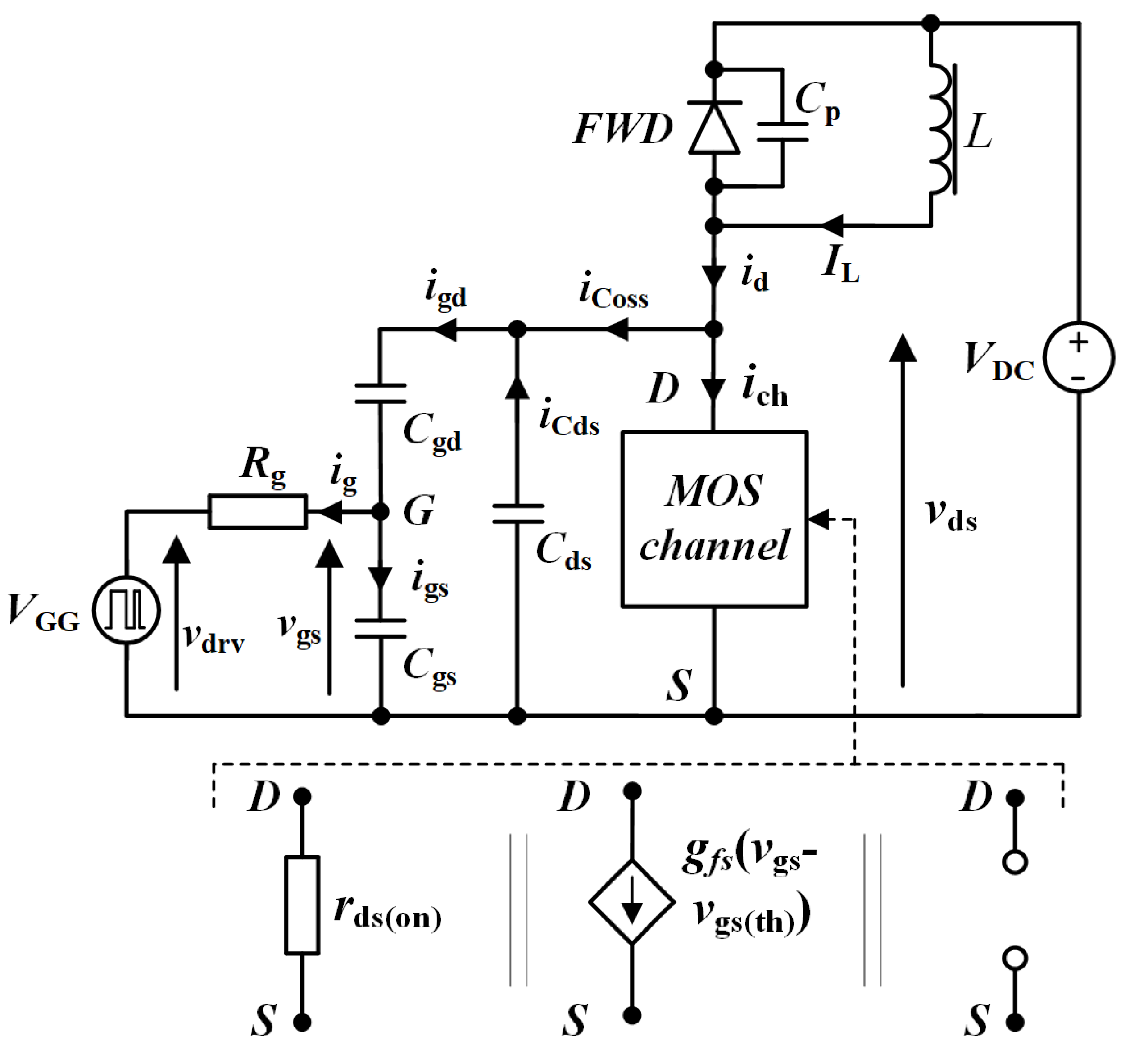
The turn-off process of SiC MOSFETs differs from the waveforms described in the literature for traditional Si MOSFETs [19]. This is due to the superior parameters of SiC devices in comparison to Si, in particular, lower junction capacitances [2,20]. To analyze the turn-off of a SiC MOSFET, an equivalent model with a driving circuit included in the transient in-pulse test setup is introduced in Figure 1. Apart from parasitic junction capacitances (, , and ), the presented model consists of a MOSFET channel that can be represented as a resistance, , voltage-dependent current source described with a transconductance parameter or an open circuit, depending on the stage of the turn-off process. The driving circuit involves gate resistance , which is the sum of the transistor internal and external resistances, and voltage source , which could take positive and negative values. Additionally, the circuit includes a DC voltage source , freewheeling diode (FWD), and inductor L, as in a standard pulse test arrangement. It is assumed that over the entire examined period, the inductor current takes a constant value.
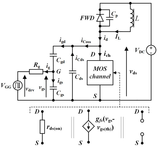
Figure 1.
The SiC MOSFET model during turn-off.
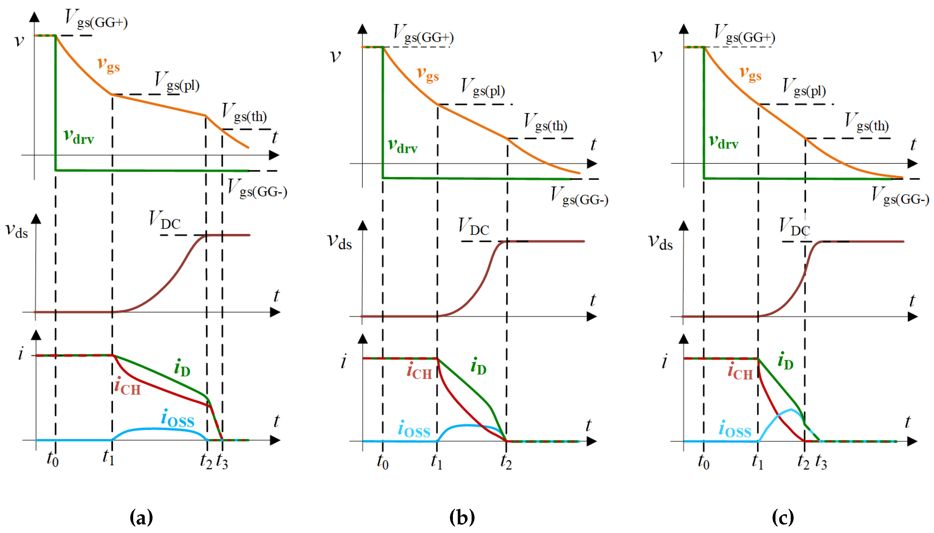
In the case of a SiC MOSFET, the turn-off waveforms depend on the switching conditions. Three general instances of the turn-off process can be distinguished. The first is a conventional one. In this case, the transistor’s voltage rises to the value before the channel current collapses to zero. The second option is a border case in which the voltage reaches and the current reaches zero at the same time. In the last one, the current reaches zero before the voltage rises to the value. The last two of the mentioned cases could be achieved for low and/or a low transistor turn-off current . Moreover, for the second and third instances, the turn-off loss is reduced [11,16,21]. The described cases are depicted in Figure 2a–c.
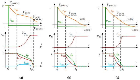
Figure 2.
The SiC MOSFET turn-off switching waveforms under different conditions: (a) standard turn-off, (b) under low current/gate resistance, and (c) with additional capacitance.
The turn-off process of an SiC MOSFET begins at the time when the off signal from the master controller is changed, at . The driving voltage source takes a value equal to (negative). In all three cases, the gate current charges the input capacitance (the sum of and , where is discharging, and is charging). This interval ends when the gate–source voltage reaches a plateau value at , which is described as:
where is the threshold voltage of the MOSFET. After in each case, the voltage starts to rise with a slew rate, according to the following formula:
where is the output capacitance of the MOSFET (the sum of and ). During the voltage rising time (between and ), some parts of the current charge the parasitic capacitance () of FWD. Therefore, the drain current of the MOSFET decreases (see Figure 2). Simultaneously, the gate current continues charging , as shown below:
However, unlike in Si MOSFETs, where, in the plateau region, is assumed to be approximately constant, in SiC MOSFETs, because of the lower values of , the voltage decreases during this period. The channel current is controlled via voltage :
which also lowers. Nevertheless, in a standard turn-off event, at the end of the voltage rising time, the voltage is above the level. Therefore, after the voltage reaches the value of , is greater than 0. The waveforms presented in Figure 2b,c show a situation with lowered and/or with a low turn-off current . The decreased value of increases the gate current (see Equation (3)), which accelerates the closing of the MOSFET channel. In the case of reduced , a large part of the current flows through the capacitance, which reduces the current and causes it to reach a zero value faster. Therefore, in the cases presented in Figure 2b,c, the voltage reaches the level during the voltage rising time. Consequently, reaches 0 at , which corresponds to the voltage reaching the level (see Figure 2b) or even before the end of the increase (see Figure 2c). In the last stage of the turn-off process (after ), the remaining part of falls until it reaches 0. Nonetheless, in the standard case, the current flows through the channel of the transistor (equal ) at , even with voltage; as in the case presented in Figure 2b, the current falls to 0 at ( is equivalent to ), and in the case presented in Figure 2c, between and , is a capacity current equal to under a voltage lower than .
The SiC MOSFET turn-off losses are equal to the integral of the current and voltage during the – periods, as depicted in the simplified waveforms in Figure 2 and according to Equation (5). Simultaneously, the turn-off losses, following those in Figure 2, may be reduced by shortening the turn-off time using a lower gate resistance. However, shortening the turn-off time increases the ddt and ddt ratios, which leads to enlarged electromagnetic interference (EMI) and transistor voltage overshoots due to parasitic inductances. Moreover, using a low gate resistance also requires a gate driver with high-current capability.
Finally, the MOSFET turn-off time could be reduced without inducing additional turn-off losses by adding an auxiliary capacitor in parallel to the transistor, as studied further in this paper. In such a circuit, the behaviors of the transistor, parasitic capacitance currents, and transistor voltages are similar to those in normal operation, as shown in Figure 2, albeit with replacing the capacitance as the sum of capacitances and . The auxiliary capacitor takes over part of the transistor current and reduces the ddt ratio, which further leads to lowered turn-off losses, according to Equation (5). Based on the concept that the auxiliary capacitor absorbs part of the transistor current, the technique is named the sink capacitor technique (SCT).
3. Laboratory Model and Experimental Results
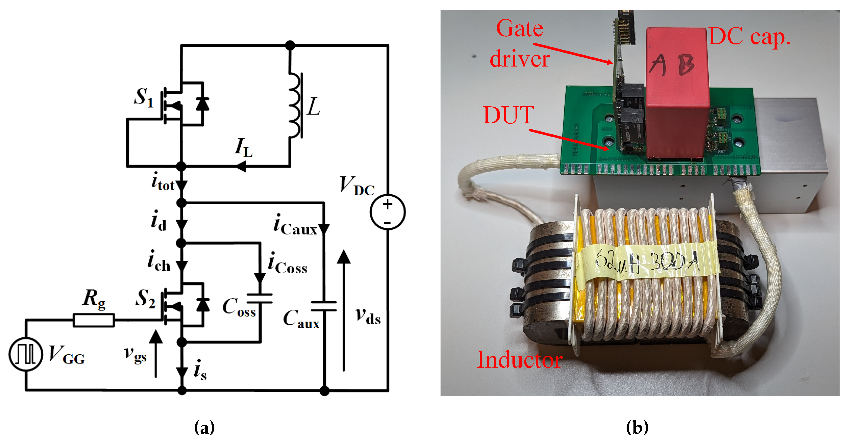
To verify the theoretical considerations on reducing turn-off losses by using an additional capacitor connected in parallel to power a MOSFET SiC transistor, a one-pulse laboratory model was built. A simplified schematic of the test setup is shown in Figure 3a, while a photo of the prototype is shown in Figure 3b. To build the laboratory model, 1200 V 40 m SiC MOSFET transistors (MSC040SMA120B4) encapsulated in TO-247-4 were used as the device under testing (DUT) and the freewheeling diode, as they are characterized by low capacitances ( = 1990 pF, = 17 pF, and = 156 pF), which is beneficial for the SCT technique, especially considering the output capacitance . Furthermore, the setup consisted of a 62 H inductor and a gate driver (UCC21750). For testing, a Tektronix oscilloscope (MSO46) with voltage probes (THDP0100; accuracy ± 2%) and a CWT Mini50HF rogowski coil were used for the measurement of the current (a typical accuracy of ±2.0%). Experiments were carried out for the different values of the transistor turn-off currents, gate resistors, and sink capacitors. Specific data on the built one-pulse laboratory test setup are listed in Table 1.

Figure 3.
One-pulse test circuits: (a) simplified schematic, (b) laboratory model.

Table 1.
Parameters of the OPT.
The testing procedure was as follows: During experiments, transistor (FWD) was turned off, while transistor (DUT) was switched via one-pulse signal. When the switch is turned on, the transistor current flows through the voltage source , inductor L, and transistor . The transistor turn-off current is determined using its turn-on time, as the current is proportional to the transistor turning on time, in accordance with Equation (6). After the transistor turns off, the current flows mainly through inductor L, and the forward-biased body diode of transistor (until the inductor current reduces to zero). Apart from this, the current flows through the auxiliary and parasitic capacitances of the laboratory model components.
where is transistor turn-on time.
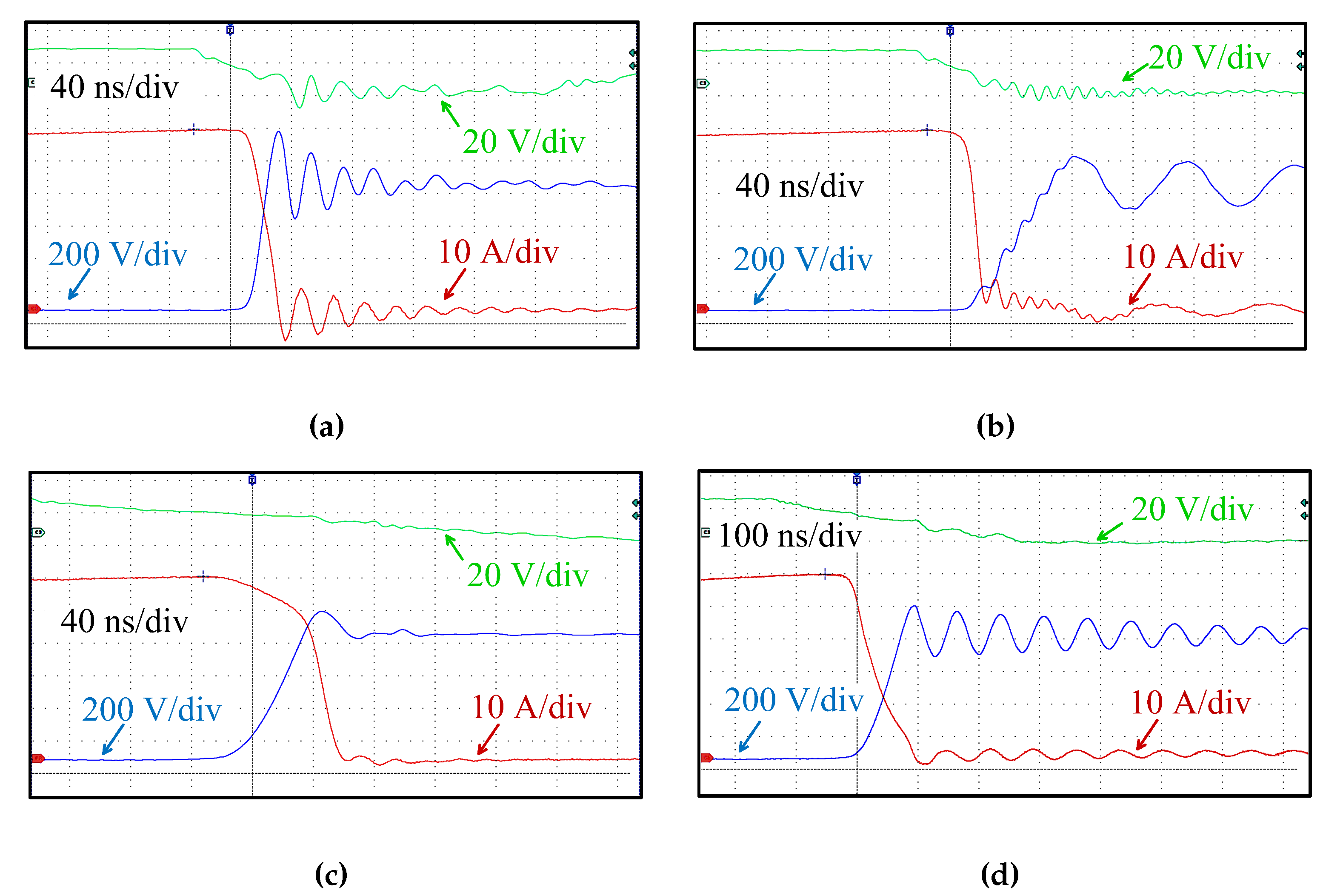
During testing, the following values were measured and recorded: transistor drain current , transistor drain–source voltage , and transistor gate–source voltage . The experiments were carried out with two different values of sink capacitances = 1 nF and 3 nF, as well as without a sink capacitor. Furthermore, three different external gate resistances were considered, as well as a supply voltage of = 800 V, with various transistor turn-off currents, with a maximum current of roughly = 60 A. Four waveforms for two different gate resistance values and two different auxiliary capacitances are shown in Figure 4.
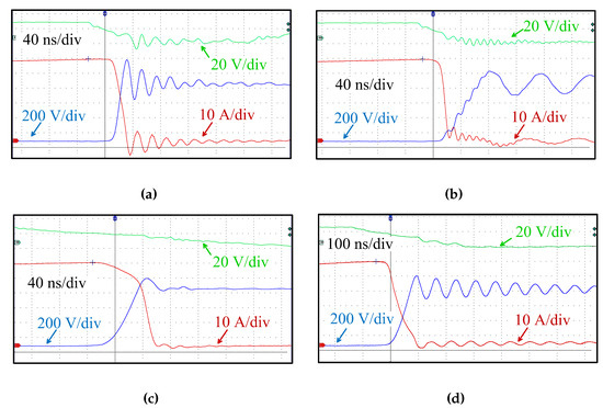
Figure 4.
Waveforms of transistor turn-off process for the different values in gate resistance and sink capacitor: (a) , (b) nF, (c) , (d) nF.
In accordance with the theoretical analysis, the value of gate resistance exerts a large effect on the voltage rising time (defined as the time required to increase the voltage from 10% to 90% of its steady-state value during the turning off of the transistor). These intervals are approximately 12 ns for and roughly 37 ns for in the case without auxiliary capacitance (Figure 4). As can be seen, the voltage rising time depends greatly on the sink capacitor value. For , due to the use of capacitance, an increase in rising time from 12 ns to 35 ns was observed. Similarly, for , the time increases from 37 ns to 48 ns. However, the enlarged voltage rising time using an additional capacitor did not have a negative effect on transistor turn-off losses. On the contrary, these were lowered—the transistor current slope ddt depends not only on the transistor gate circuit but also differs based on whether the sink capacitor is employed or not. When it is used, the transistor current drops to zero faster. Simultaneously, as previously mentioned, using an additional auxiliary capacitance increases the voltage rising time. These two reasons resulted in lower turn-off losses for the transistor when using the sink capacitor technique, which is accordance with Equation (5). To prove this, an analysis of transistor turn-off losses, circuit currents, and voltages is presented in the following sections.
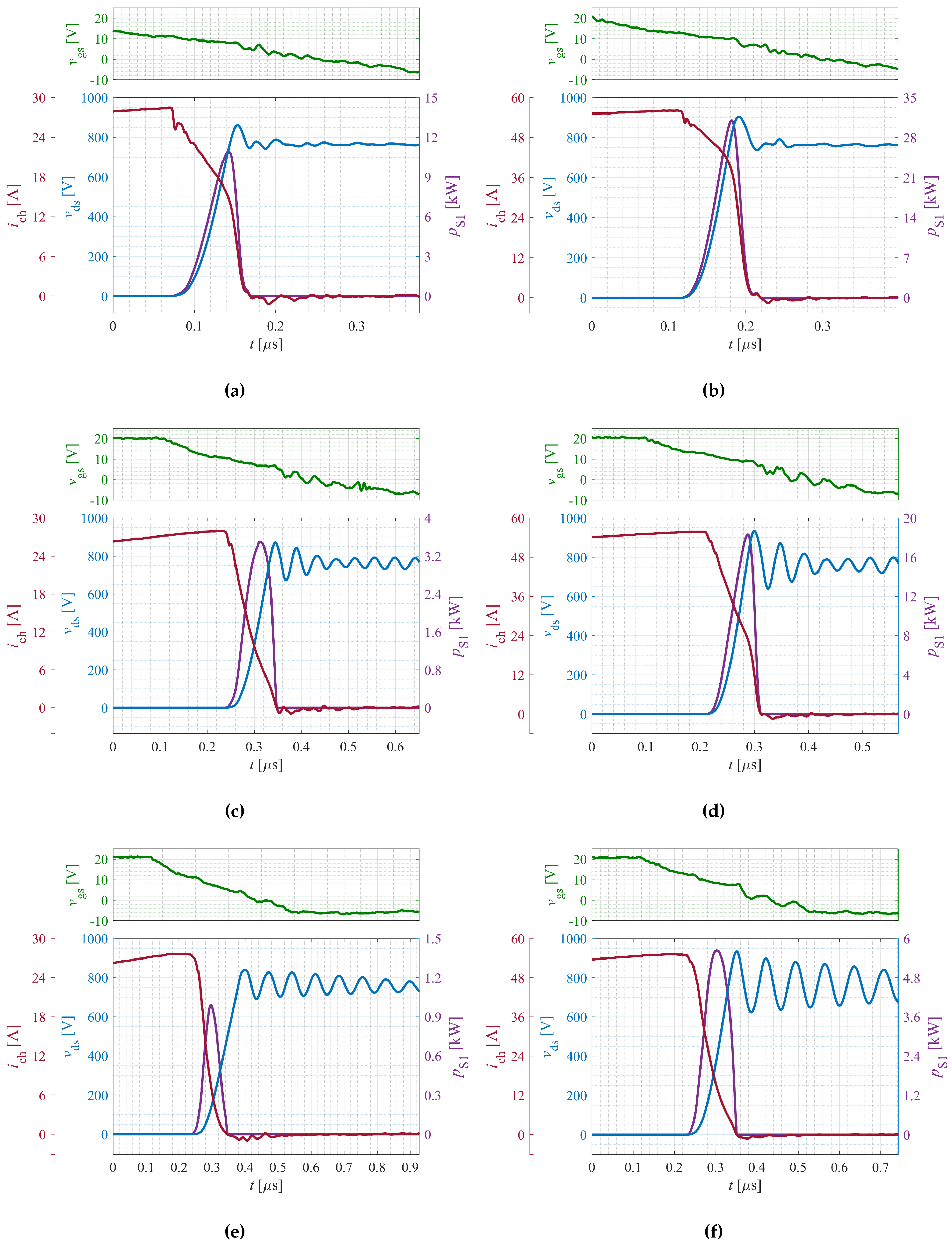
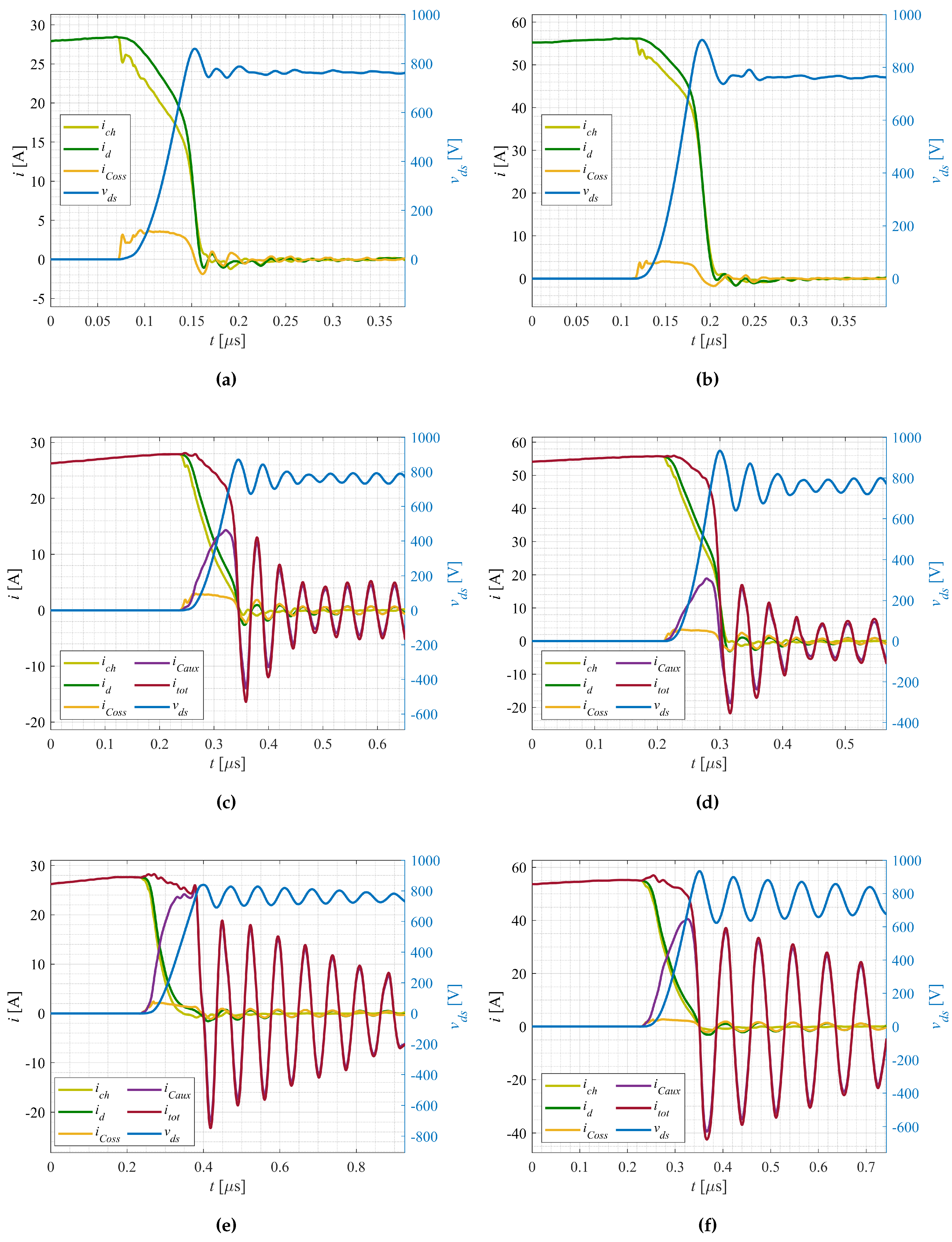
Figure 5 and Figure 6 show waveforms obtained via one-pulse laboratory tests and processed using MATLAB 2023b software. Here, the drain current was measured during experiments, while the currents and were estimated on the basis of the and capacitances and the measured voltage, according to Equations (7) and (8). The output capacitance was estimated using the datasheet-based characteristic, taking into account the capacitance dependence on the voltage. Figure 5 and Figure 6 show the results for the gate resistance , the two different transistor turn-off currents A, and a circuit with and without sink capacitances ( nF). The turn-off power is calculated following Equation (11).
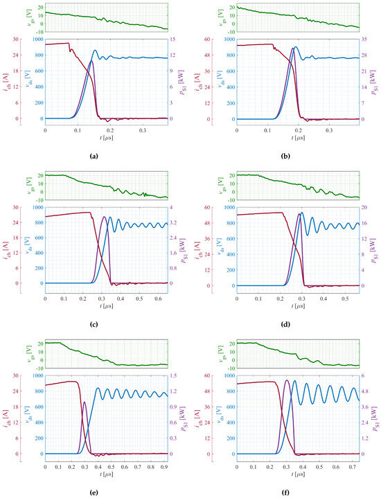
Figure 5.
Transistor (green) and (blue) voltages, (red) current and power (violet) during turn-off process for ; different values of current and sink capacitor: (a) A, , (b) A, , (c) A, nF, (d) A, nF, (e) A, nF, (f) A, nF.
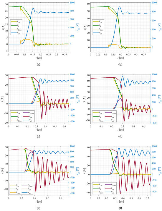
Figure 6.
One-pulse test circuit currents and voltage during transistor turn-off process for ; different current and auxiliary capacitor values: (a) A, , (b) A, , (c) A, nF, (d) A, nF, (e) A, nF, (f) A, nF.
The channel current is calculated as the difference between the measured current and the estimated current, as in Equation (9):
The sum of the total calculated current is given by:
Turn-off power is calculated in accordance with Equation (11):
As depicted in Figure 5, transistor turn-off losses decrease with an increasing value in the capacitance and decrease with transistor turn-off currents. Moreover, a higher value of leads to reduced ddt and ddt ratios. The change in the current shape mainly occurs during the increase in the voltage. For example, for a case without a sink capacitor and a transistor turn-off current equal to 60 A, the current during the process of increasing voltage increases from 0 to 800 V and the transistor channel current reduces from 56 A to 45 A. However, for sink capacitances equal to 1 nF and 3 nF, the established current variances were from 59 A to 24 A and 57 A to 3 A, respectively. That difference in transistor current reduction causes a substantial effect on turn-off losses.
Figure 5 shows the transistor voltage and measured and estimated currents. For the analyzed cases, it can be stated that there is a minor influence of the employed sink capacitance on the shape of the current . However, the value of the capacitance is crucial considering the value of the capacitance current . Thus, during commutation, the channel current changes significantly, according to Equation (10). Simply, the sink capacitance takes over part of the transistor current during turning off, lowering the channel current, and as the channel current is the crucial source of power losses [22], these are also advantageously limited. However, a notable drawback of the described technique for achieving soft switching behavior is the excessive ringing of the voltage after the turn-off process has resolved. This is caused by a resonance between the capacitances of the power semiconductor devices and the sink capacitance and the parasitic inductances inevitably apparent in the circuit, e.g., because of the connections. The resonant currents, as shown in Figure 5, are of notable values. For example, considering a case with nF, the current overshoots exceeded 50% of the switched currents. Nevertheless, these currents can be eliminated through conventional snubber circuits [15,19].
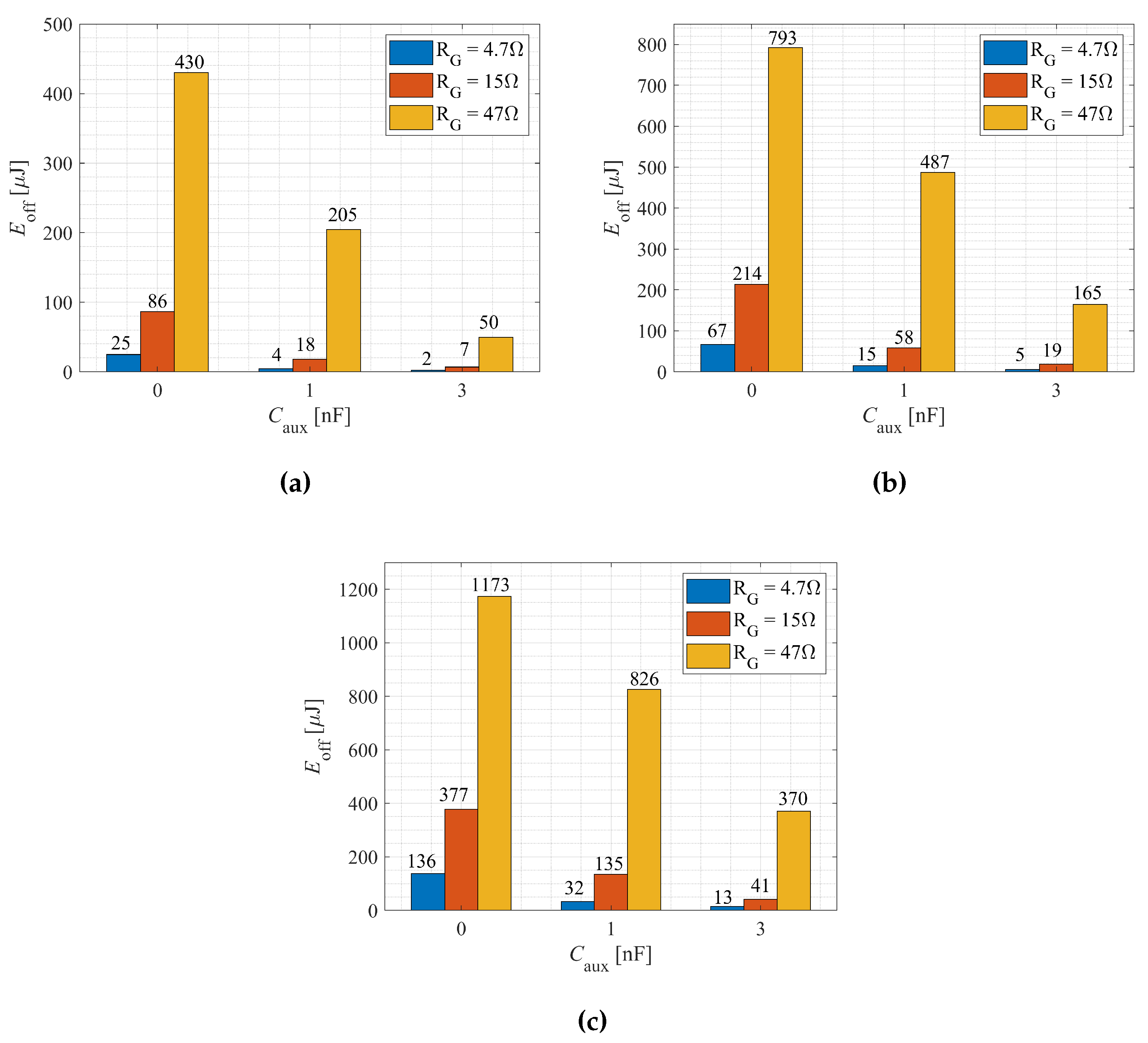
A power loss comparison is depicted in Figure 7. Here, the turn-off losses are shown for three values of gate resistance , with and without two different sink capacitances , as well as for three different switched currents. For a case with a 60 A turn-off switched current and the highest considered gate resistance , the turn-off losses are J with the sink capacitor , and J and J for auxiliary capacitance at 1 nF and 3 nF, respectively. For the smallest tested gate resistance , the losses for different capacitance values are J, J, and J. When a sink capacitor nF was employed for the experiment with a gate resistance of , a turn-off power loss reduction by slightly over threefold was achieved. For the identical sink capacitance used for the test with , the loss reduction was higher than tenfold. The proportions between the turn-off losses for different configurations are similar for the three studied switched currents and two tested gate resistances and . This was not the case for , as for such a high gate resistance, the transistor’s channel current is still higher than zero, even though the voltage has already reached its nominal value (case depicted in Figure 2a). All in all, as shown based on the experiments, the current sink capacitor technique can be effectively employed to diminish the turn-off power losses to a great extent.
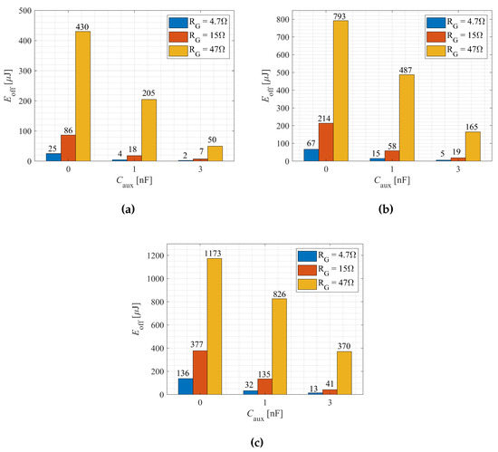
Figure 7.
Transistor turn-off loss comparison for different turn-off currents: (a) A, (b) A, (c) A.
4. Discussion
In [17], the authors state that the soft turn-off limit of the transistor is reached when, during the turn-off process, the channel current reaches zero and the voltage equals the supply voltage value (800 V in the conducted studies) at the same moment. This scenario is illustrated in Figure 5c. However, as demonstrated based on the experimental study, additional increases in capacitance or decreases in the gate resistor value beyond the suggested soft turn-off limit in [17] allowed for a further reduction in turn-off losses. In Figure 7a, for the considered critical case, the turn-off losses were 205 µJ; reducing the gate resistor from to and enabled a significant reduction in turn-off losses to 18 µJ and 4 µJ, respectively. Similarly, increasing the sink capacitor from nF to nF resulted in a decrease in losses from 205 µJ to 50 µJ. Thus, the choice of optimal current sink capacitance is not trivial.
Fully appropriate and accurate models of the turn-off process of SiC MOSFETs have still not been presented in the literature, as taking into account all parasitic elements present in the circuit and the various phenomena still hindering SiC MOSFETs, such as charge traps [23] or drain-induced barrier lowering (DIBL) [24], is a very challenging task [20,21]. Therefore, we recommend an experimental approach to choosing the proper capacitance value. Considering that the single-pulse test setup is very simple to arrange and experiment with and that many engineers perform such tests prior to designing full converters to estimate the power losses anyway, conducting transistor turn-off tests for various sink capacitors in real-world circuits would help to establish the optimal capacitance for each specific application.
5. Conclusions
In this paper, an experimental study on turn-off power loss reduction employing a small auxiliary capacitor connected in parallel to the transistor is conducted. The described current sink capacitor technique is aimed at circuits operating with ZVS switching, e.g., converters controlled with triangular current mode (TCM) or a quasi-square wave (QSW). Based on experiments with 1200 V SiC MOSFETs, it is shown that applying the current sink capacitor technique, a turn-off power loss reduction of over tenfold can be attained. The scale of the improvement is highly dependent on the gate resistance, as well as the value of the sink capacitor. Furthermore, to maximize the power loss reduction potential, the technique should be used with advanced gate drivers with high-current capability.
In summary, the technique can be effectively used to minimize the turn-off power losses by a substantial value. The method is especially attractive as it is very simple and requires only very small capacitors, with values in the range of single nanofarads, e.g., C0G SMD capacitors could be employed. Thus, considering whole power converters, the volume increase is essentially negligible, thereby limiting the impact of the converter’s power density. Therefore, using the current sink capacitor technique may be deemed beneficial for constructing high-performing, high-power-density soft-switched converters.
Author Contributions
Conceptualization, M.H., R.K. and P.T.; methodology, M.H., R.K. and P.T.; software, M.H. and R.M.; hardware preparation, M.H. and R.M.; experimental validation, M.H., R.K. and P.T.; original draft preparation, M.H., R.K. and P.T.; writing—review and editing, M.H., R.K. and P.T.; visualization, M.H., R.K. and P.T.; supervision, J.R.; project administration, J.R.; funding acquisition, J.R. All authors have read and agreed to the published version of the manuscript.
Funding
The research leading to these results received funding from EEA/Norway Grants 2014–2021.
Data Availability Statement
Data are contained within the article.
Conflicts of Interest
The authors declare no conflicts of interest.
References
- She, X.; Huang, A.Q.; Lucia, O.; Ozpineci, B. Review of Silicon Carbide Power Devices and Their Applications. IEEE Trans. Ind. Electron. 2017, 64, 8193–8205. [Google Scholar] [CrossRef]
- Zhang, L.; Yuan, X.; Wu, X.; Shi, C.; Zhang, J.; Zhang, Y. Performance Evaluation of High-Power SiC MOSFET Modules in Comparison to Si IGBT Modules. IEEE Trans. Power Electron. 2019, 34, 1181–1196. [Google Scholar] [CrossRef]
- Gonzalez, J.O.; Wu, R.; Jahdi, S.; Alatise, O. Performance and Reliability Review of 650 V and 900 V Silicon and SiC Devices: MOSFETs, Cascode JFETs and IGBTs. IEEE Trans. Ind. Electron. 2020, 67, 7375–7385. [Google Scholar] [CrossRef]
- Wang, Z.; Wu, Y.; Mahmud, M.H.; Zhao, Z.; Zhao, Y.; Mantooth, H.A. Design and Validation of A 250-kW All-Silicon Carbide High-Density Three-Level T-Type Inverter. IEEE J. Emerg. Sel. Top. Power Electron. 2020, 8, 578–588. [Google Scholar] [CrossRef]
- Li, H.; Zhang, Z.; Wang, S.; Tang, J.; Ren, X.; Chen, Q. A 300-kHz 6.6-kW SiC Bidirectional LLC Onboard Charger. IEEE Trans. Ind. Electron. 2020, 67, 1435–1445. [Google Scholar] [CrossRef]
- Zeng, J.; Zhang, G.; Yu, S.S.; Zhang, B.; Zhang, Y. LLC resonant converter topologies and industrial applications—A review. Chin. J. Electr. Eng. 2020, 6, 73–84. [Google Scholar] [CrossRef]
- Pahlevani, M.; Jain, P.K. Soft-Switching Power Electronics Technology for Electric Vehicles: A Technology Review. IEEE J. Emerg. Sel. Top. Ind. Electron. 2020, 1, 80–90. [Google Scholar] [CrossRef]
- Hazra, S.; Madhusoodhanan, S.; Moghaddam, G.K.; Hatua, K.; Bhattacharya, S. Design Considerations and Performance Evaluation of 1200-V 100-A SiC MOSFET-Based Two-Level Voltage Source Converter. IEEE Trans. Ind. Appl. 2016, 52, 4257–4268. [Google Scholar] [CrossRef]
- Christen, D.; Biela, J. Analytical Switching Loss Modeling Based on Datasheet Parameters for mosfets in a Half-Bridge. IEEE Trans. Power Electron. 2019, 34, 3700–3710. [Google Scholar] [CrossRef]
- Rąbkowski, J.; Zdanowski, M.; Kopacz, R.; Gonzalez-Hernando, F.; Villar, I.; Larrañaga, U. From the Measurement of C OSS – VDS Characteristic to the Estimation of the Channel Current in Medium Voltage SiC MOSFET Power Modules. IEEE Trans. Instrum. Meas. 2023, 72, 1–10. [Google Scholar] [CrossRef]
- Xie, Y.; Chen, C.; Yan, Y.; Huang, Z.; Kang, Y. Investigation on Ultralow Turn-off Losses Phenomenon for SiC MOSFETs with Improved Switching Model. IEEE Trans. Power Electron. 2021, 36, 9382–9397. [Google Scholar] [CrossRef]
- Fritz, N.; Engelmann, G.; Stippich, A.; Ludecke, C.; Philipps, D.A.; Doncker, R.W.D. Toward an In-Depth Understanding of the Commutation Processes in a SiC MOSFET Switching Cell Including Parasitic Elements. IEEE Trans. Ind. Appl. 2020, 56, 4089–4101. [Google Scholar] [CrossRef]
- Roy, S.K.; Basu, K. Analytical Model to Study Hard Turn-off Switching Dynamics of SiC mosfet and Schottky Diode Pair. IEEE Trans. Power Electron. 2021, 36, 861–875. [Google Scholar] [CrossRef]
- Cao, J.; Zhou, Z.K.; Shi, Y.; Zhang, B. On-Chip Active Turn-Off Driving Technique to Prevent Channel Current From Disappearing Prematurely in SiC MOSFET’s Applications. IEEE Trans. Circuits Syst. II Express Briefs 2023, 70, 660–664. [Google Scholar] [CrossRef]
- Yang, X.; Xu, M.; Li, Q.; Wang, Z.; He, M. Analytical Method for RC Snubber Optimization Design to Eliminate Switching Oscillations of SiC MOSFET. IEEE Trans. Power Electron. 2022, 37, 4672–4684. [Google Scholar] [CrossRef]
- Song, S.; Peng, H.; Chen, X.; Xin, Q.; Kang, Y. Determination and Implementation of SiC MOSFETs Zero Turn Off Loss Transition Considering No Miller Plateau. IEEE Trans. Power Electron. 2023, 38, 15509–15521. [Google Scholar] [CrossRef]
- Roy, S.K.; Basu, K. Analytical Model to Study Turn-OFF Soft Switching Dynamics of SiC MOSFET in a Half-Bridge Configuration. IEEE Trans. Power Electron. 2021, 36, 13039–13056. [Google Scholar] [CrossRef]
- Kopacz, R.; Harasimczuk, M.; Trochimiuk, P.; Rąbkowski, J. Investigation of Soft-Switching QSW Technique in DC/DC SiC-Based Flying Capacitor Converter with Q2L Control. IEEE Trans. Ind. Electron. 2023, 70, 9035–9045. [Google Scholar] [CrossRef]
- Mohan, N.; Undeland, T.; Robbins, W. Power Electronics: Converters, Applications, and Design, 3rd ed.; John Wiley & Sons: Hoboken, NJ, USA, 2002. [Google Scholar]
- Chen, K.; Zhao, Z.; Yuan, L.; Lu, T.; He, F. The Impact of Nonlinear Junction Capacitance on Switching Transient and Its Modeling for SiC MOSFET. IEEE Trans. Electron Devices 2015, 62, 333–338. [Google Scholar] [CrossRef]
- Agrawal, B.; Preindl, M.; Bilgin, B.; Emadi, A. Estimating switching losses for SiC MOSFETs with non-flat miller plateau region. In Proceedings of the 2017 IEEE Applied Power Electronics Conference and Exposition (APEC), Tampa, FL, USA, 26–30 March 2017; pp. 2664–2670. [Google Scholar] [CrossRef]
- Rabkowski, J.; Gonzalez-Hernando, F.; Zdanowski, M.; Villar, I.; Larranaga, U. Real E OFF as a factor in design of soft-switched DC-DC converters with SiC MOSFET power modules. In Proceedings of the 2022 IEEE Energy Conversion Congress and Exposition (ECCE), Detroit, MI, USA, 9–13 October 2022; pp. 1–6. [Google Scholar] [CrossRef]
- Chaturvedi, M.; Dimitrijev, S.; Haasmann, D.; Moghadam, H.A.; Pande, P.; Jadli, U. Comparison of Commercial Planar and Trench SiC MOSFETs by Electrical Characterization of Performance-Degrading Near-Interface Traps. IEEE Trans. Electron Devices 2022, 69, 6225–6230. [Google Scholar] [CrossRef]
- Hofstetter, P.; Maier, R.W.; Bakran, M.M. Influence of the Threshold Voltage Hysteresis and the Drain Induced Barrier Lowering on the Dynamic Transfer Characteristic of SiC Power MOSFETs. In Proceedings of the 2019 IEEE Applied Power Electronics Conference and Exposition (APEC), Anaheim, CA, USA, 17–21 March 2019; pp. 944–950. [Google Scholar] [CrossRef]
Disclaimer/Publisher’s Note: The statements, opinions and data contained in all publications are solely those of the individual author(s) and contributor(s) and not of MDPI and/or the editor(s). MDPI and/or the editor(s) disclaim responsibility for any injury to people or property resulting from any ideas, methods, instructions or products referred to in the content. |
© 2023 by the authors. Licensee MDPI, Basel, Switzerland. This article is an open access article distributed under the terms and conditions of the Creative Commons Attribution (CC BY) license (https://creativecommons.org/licenses/by/4.0/).