Article

A Spread-Spectrum Modulation Scheme for a 3 × 6 Indirect Matrix Converter Based on a Current Ripple Model

1
Tianjin Key Laboratory of Intelligent Control of Electrical Equipment, Tiangong University, Tianjin 300387, China
2
Zhejiang University Advanced Electrical Equipment Innovation Center, Hangzhou 311107, China
*
Author to whom correspondence should be addressed.
Energies 2024, 17(11), 2546; https://doi.org/10.3390/en17112546
Submission received: 8 April 2024 / Revised: 16 May 2024 / Accepted: 23 May 2024 / Published: 24 May 2024
(This article belongs to the Special Issue Advanced Power Electronics Technology)

Abstract

:
Focused on addressing harmonic suppression in multiphase indirect matrix converters (IMCs), this study explores spread-spectrum modulation technology through ripple analysis calculations. We introduce a current ripple spread-spectrum modulation (CR-SSM) method tailored for multiphase IMC systems. In this approach, a 3 × 6-phase IMC is modeled as a two-port network, and a small-signal model of the output side is established. The transfer function is utilized to analyze the two-port network in the complex frequency domain (s-plane). The time-domain expression of the output current ripple is derived in vector form. Subsequently, the distribution of the output ripple and locus are determined based on specified constraints. The carrier frequency is dynamically adjusted online according to the specified ripple locus. Compared to classical periodic PWM methods, this approach offers a broader range of frequency variations and achieves a more uniform output spectrum. Furthermore, CR-SSM optimizes system efficiency and enhances spread-spectrum modulation. Experimental results demonstrate that this method effectively enhances the quality of input and output waveforms in multiphase IMC systems.

1. Introduction

The indirect matrix converter (IMC) represents a form of “all-silicon” AC/AC direct power converter [1]. This converter achieves efficient power conversion without requiring an energy storage link, owing to its compact structure, ability to deliver sinusoidal input–output waveforms, adjustable input power factor, low harmonic distortion, flexible phase adjustment of input current, and other noteworthy features. The IMC has proven highly effective in applications within the green energy sector [2,3].
In a three-phase system, the conventional configuration of a matrix converter (MC) is referred to as a direct matrix converter (DMC), featuring a 3 × 3 bidirectional switch array [4]. A multiphase indirect matrix converter (IMC) comprises a three-phase rectifier stage and a six-phase inverter stage, each divided into distinct structural and functional segments. As illustrated in Figure 1, the rectifier stage of the IMC resembles a current source rectifier (CSR). Conversely, the inverter stage of the IMC is designed to function as two two-level voltage source inverters (VSIs) [5]. The clamper circuit is specifically implemented for protective purposes and does not actively facilitate energy transfer. The inherent design of the IMC allows for direct energy transfer between input and output, but it also enables the transmission of harmonic distortion from one side of the converter to the other. The study by [6] enhances the understanding of IMC topology, indicating that the input filter plays a critical role in the converter system by attenuating high-frequency harmonics to prevent interference with the normal operation of other equipment at their common connection point. Additionally, it assists in smoothing out discrete input current to generate a continuous sinusoidal current waveform on the source side. One fundamental and widely used method for improving waveform quality in frequency converters is by increasing the carrier frequency of the controller. Recent advancements in wide bandgap semiconductors, such as silicon carbide (SiC), have significantly expanded the feasible carrier frequency of power converters [7,8,9]. Various approaches have been proposed to enhance the effectiveness of power converters using pulse-width modulation (PWM), including optimization techniques for vector selection among available vectors [10], reduction in common-mode components in modulation waves [11,12], refinement of switch sequences [13,14,15], and enhancement of carrier properties [16,17,18].
Spread-spectrum modulation (SSM) is an ideal strategy for reducing EMI in multiphase IMC systems. Common SSM strategies currently include random PWM, programmed PWM, and periodic PWM. In comparison to random PWM, periodic PWM uses a predetermined frequency density function to dynamically change the carrier frequency, achieving a fixed EMI spectrum [19]. By varying the carrier frequency, periodic PWM introduces additional modulation flexibility. Typical carrier waveforms encompass sinusoidal, exponential, and triangular shapes. Dual Fourier analysis of inverter output voltages reveals that triangular wave frequency density functions offer smoother spectral performance compared to sinusoidal and exponential carriers, which exhibit distinct spectral peaks at specific frequencies [20]. Research on the variation pattern of periodic signal frequency and waveform under equal maximum frequency deviation is explored in [21], which derives an optimal segmented modulation signal for superior EMI suppression by optimizing a combination of three frequency density functions. Furthermore, reference [22] employs a variable density sawtooth carrier to implement periodic PWM, thus achieving a spread-spectrum effect while reducing inverter switch frequencies. Reference [23] explores a spread-spectrum modulation scheme by varying switch frequencies according to uniform distribution, exponential distribution, and normal distribution and derives corresponding equations. Experimental results demonstrate that the proposed spread-spectrum modulation scheme can reduce EMI by 20 dB. Reference [24] proposes an algorithm using sinusoidal-wave pulse-width modulation (PWM) to suppress conducted-mode (CM) EMI in large-scale networks. This method minimizes switch frequency overlap between converters, thereby reducing total EMI levels. The authors of [25,26] focus on using Σ-Δ modulation for voltage source converters. The proposed modulation techniques significantly reduce switching losses and reduce lower-order harmonics by varying switch frequencies. Additionally, Y. Huang utilizes a variable frequency density sawtooth carrier to achieve periodic PWM, thereby achieving spread-spectrum effects while reducing inverter switch frequencies [27]. Reference [28] presents an optimized periodic PWM scheme that minimizes motor vibration frequency response peaks by considering the motor’s vibration frequency response function. Reference [29] details the impact of periodic PWM on the current harmonics of permanent magnet synchronous motors (PMSMs). Experimental evidence demonstrates that periodic PWM disperses high-frequency harmonics across wider frequency bands, thereby suppressing peak harmonics. Reference [30] proposes a spectral analysis method based on periodic PWM and dual Fourier series to reduce current harmonics in active power filters. Reference [31] introduces a novel PWM strategy based on uniform distribution PWM and experimentally verifies its effectiveness in eliminating EMI peaks, reducing conducted EMI, and minimizing switch losses. Reference [32] analyzes the suppression of harmonics and common-mode EMI using periodic PWM, validating the accuracy of theoretical analysis and the effectiveness of algorithms through experiments.
However, the widespread implementation of current-ripple-based spread-spectrum modulation (CR-SSM) in multiphase inverter motor control (IMC) systems still encounters several challenges. Firstly, variations in vector amplitudes of the rectifier and inverter stages within the IMC, influenced by the DC-link voltage, pose difficulties in establishing a consistent ripple model. Secondly, the presence of input filters can affect waveform quality at the grid side and complicate the analysis of the impact of input switching sequences and transmission ratios on the output current ripple locus. Additionally, the resonant frequency and bandwidth of filters impose limitations on the range of carrier frequency variations.
To address these challenges, this study investigates the combined impact of the rectifier and inverter stages in a 3 × 6-phase inverter motor control (IMC) system [33,34]. It involves an analysis of a small-signal model at the output stage to derive a time-domain expression for the output current ripple. Finally, based on the constraints related to ripple distribution and ripple index, the CR-SSM (current ripple spread-spectrum modulation) method is proposed. This method allows for a broader range of frequency fluctuations while ensuring safe commutation and achieving higher-quality spread-spectrum modulation. The main contributions of this paper are outlined as follows:
  • Through the establishment of a small-signal model on the output side, the locus of the output current ripple can be determined. Furthermore, dynamically adjusting the carrier frequency based on the ripple locus can effectively broaden the harmonic spectrum, improve total harmonic distortion, and enhance output modulation efficiency.
  • The CR-SSM method dynamically adjusts the carrier frequency based on the ripple locus. The CR-SSM method is based on the output current ripple, and thus the debugging process of traditional periodic PWM is eliminated. It standardizes the construction of carrier frequencies, providing clear numerical indicators and improving frequency fluctuation efficiency. Furthermore, it reduces harmonic spikes at specific frequency bands and optimizes system efficiency.
The remainder of this paper is structured as follows: In Section 2, we provide a brief overview of multiphase IMC basic modulation strategies. Section 3 analyzes the voltage error locus and establishes small-signal models for multiphase IMC outputs to derive time-domain expressions for the current ripple. Subsequently, we explore achieving improved total harmonic distortion (THD) and efficiency by implementing online adjustment of carrier frequencies along the ripple locus. Section 4 presents experimental results comparing CR-SSM and classical period PWM. Finally, Section 5 summarizes the key conclusions drawn from this study.

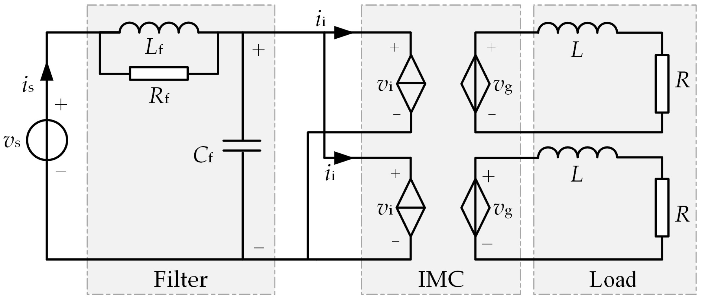
2. Modulation Method of Multiphase IMC

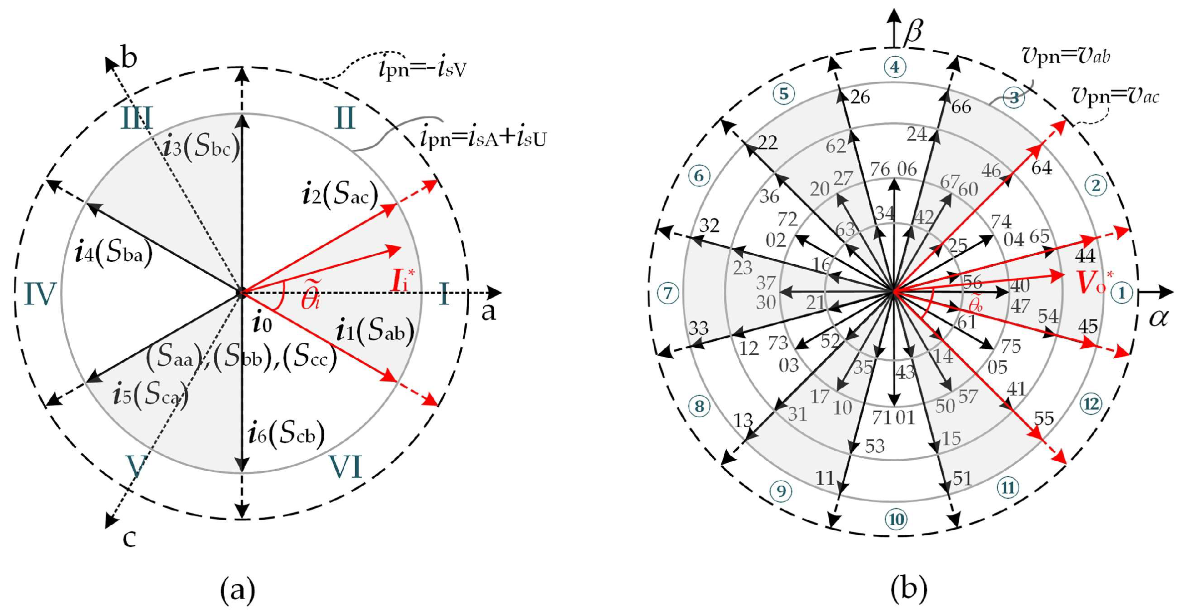
2.1. Space Vector Modulation

To enhance the utilization of input voltage and facilitate the commutation action of the switching device, we employed the indirect space vector modulation method for the multiphase IMC. Specifically, the rectifier stage adopts zero-free vector modulation based on the expected input current vector Ii*, while the inverter stage utilizes a maximum four-vector SVPWM modulation according to the anticipated output voltage vector Vo*, as illustrated in Figure 2. In this paper, the moment represented by the vector position in Figure 2 is presented as an example. The red color arrows represent the vector of the rectifier stage in the Ι sector and the inverter stage in the ① sector.
As shown in Figure 2a, the space vector plane of the rectifier is divided into six sectors, labeled as I, II, …, VI. The symbols ix (x = 1, 2, …, 6) represent the rectifier active vectors, and θ ˜ i represents the angle included between Ii* and the starting vector position of the sector.
i x = 2 3 i pn   e j ( 2 x 3 ) π / 6
I i * = 2 3 ( i a + i b   e j 2 π / 3 + i c e j 4 π / 3 )
where ipn is the DC-link current, which is related to the load current and the inverter switching state. The rectifier stage is usually modulated by two effective vectors adjacent to Ii*. The rectifier stage is responsible for synthesizing vpn and regulating the Ii* phase, and the Ii* amplitude is determined by the output current. The rectifier stage duty cycle is
d μ = sin ( π 3 θ ˜ i ) / cos ( π 6 θ ˜ i ) d υ = sin ( θ ˜ i ) / cos ( π 6 θ ˜ i )
where dμ is the duty cycle of the vector iμ (vector i1 in Figure 2); dν is the duty cycle of the vector iν (vector i2 in Figure 2). When the effective current vector iμ acts, the DC-link voltage is vab (corresponding to the input Sab), and when the effective current vector iν is acted upon, the DC-link voltage is vac (corresponding to the input Sac). Vim is the amplitude of the three-phase sinusoidal input voltage so that the average DC-link voltage can be expressed as follows:
v pn = v μ d μ + v ν d ν = 3 V im 2 cos ( π / 6 θ ˜ i )
In Figure 2a, the switching state Sab corresponds to the DC-link voltage vab. Figure 2b is a schematic diagram of the inverter stage output voltage space vector. The space vector plane of the inverter is divided into 12 sectors, labeled as ①, ②, …., ⑫. The symbols vy (y = 1, 2, …, 12) represent the inverter active vectors; v0 and v7 are the zero voltage vectors; Vo* is the desired output voltage vector; θ ˜ o represents the angle included between Vo* and the starting vector position of the sector; and vpn is the DC-link voltage.
v y = 2 3 v pn e j ( 2 y 1 ) π / 12
V o * = 2 3 ( v a + v b e j 2 π / 3 + v c e j 4 π / 3 + v u e j π / 6 + v v e j 5 π / 6 + v w e j 3 π / 2 )
The IMC voltage transmission ratio q is defined as follows:
q = V om / V im
where Vom and Vim are the desired output and input voltage vector amplitudes.
According to the vector space decoupling (VSD) transformation, each voltage vector of the inverter stage can be projected to the α-β plane and the harmonic plane x-y. Each plane contains 60 valid vectors and 4 zero vectors. While synthesizing the α-β plane fundamental voltage, it is necessary for the x-y plane output voltage to be zero [34]. Thus, a minimum of four basic vectors are required to fulfill the modulation requirements, as expressed below.
d 1 d 2 d 3 d 4 = v 1 α v 2 α v 3 α v 4 α v 1 β v 2 β v 3 β v 4 β v 1 x v 2 x v 3 x v 4 x v 1 y v 2 y v 3 y v 4 y 1 v α * v β * 0 0
where d1~d4 donate the duty cycles of the four basic vectors, namely V1(55), V2(45), V3(44), and V4(64), which are required to synthesize the output reference vector Vo*. To ensure output voltage utilization, V1, V2, V3, and V4 can be selected as four vectors that are adjacent to Vo*, d0 = 1 − d1d2d3d4 donates the duty cycle of zero vectors. Table 1 provides the applied times of voltage vectors and the switch selection of the inverter sectors ①, ②, …. ⑫ within Tc/2. V0 and V7 are zero vectors.
Given that the rectifier and inverter stages are directly cascaded, it is necessary to ensure coordination between the switching sequences of the two stages. In order to reduce switching losses, each power device is switched only once in each PWM cycle. In this paper, symmetrical triangular carrier PWM is adopted. The rectifier stage vector sequence is divided into 3 segments, and the inverter stage sequence is divided into 13 segments. The vector action sequence is shown in Figure 3. To minimize the switching action, the rectifier stage vector sequence needs to be switched from iμ-iν-iμ to iν-iμ-iν when Ii* turns from an odd sector to an even sector. Similarly, the inverter stage follows the principle of minimum switching action. Tc is a carrier cycle; dμ = Tc dμ and dν = Tc dν is the duration time of rectifier vector iμ and iν, respectively; d = Tcdμd2 is the duration time when rectifier vector iμ and inverter vector v2 are implemented.

2.2. Classical Periodic PWM

In the classical periodic PWM modulation, the carrier frequency of the multiphase IMC inverter stage is no longer constant [35,36,37,38] but varies periodically around a specific center frequency according to certain mathematical rules.
f c ( t ) = f c 0 ± Δ f c v m ( t )
where fc0 represents the center frequency of the time-varying carrier frequency, while Δfc denotes the maximum frequency deviation from the time-varying carrier frequency to the center frequency. Furthermore, vm(t) stands for a periodic signal with an amplitude within [−1, 1]. Typically, sine wave, triangular wave, and exponential wave are selected as modulation signals, which can be expressed as follows:
m ( t ) = M m sin ( 2 π f m t )
0 < t < k s T m 2 ,   m ( t ) = M m f m 2 k s t k s T m 2 < t < ( 1 k s 2 ) T m ,   m ( t ) = M m ( 1 k s ) ( 1 2 f m t ) ( 1 k s 2 ) T m < t < T m ,   m ( t ) = M m 2 k s ( f m t 1 )
where ks is the symmetry index in the range (0, 1).
0 < t < T m 4 ,   m ( t ) = M m ( e p 4 f m 1 ) ( e p t 1 ) T m 4 < t < T m 2 ,   m ( t ) = M m ( e p 4 f m 1 ) ( e p 2 f m e p t 1 ) T m 2 < t < 3 T m 4 ,   m ( t ) = M m ( e p 4 f m 1 ) ( 1 e p 2 f m e p t ) 3 T m 4 < t < T m ,   m ( t ) = M m ( e p 4 f m 1 ) ( 1 e p f m e p t )
where p is the concavity coefficient.
According to the Parseval theorem, in order to ensure constant frequency energy, the peak harmonic amplitude decreases as the bandwidth of the harmonic increases [39]. By using periodic PWM modulation, the carrier frequency is no longer fixed, so the high-frequency harmonics of multiphase IMC will not concentrate near a fixed frequency. This can greatly reduce the amplitude of high-frequency current harmonics, but there still exists some harmonic content.

3. Spread-Spectrum Modulation Based on Current Ripple

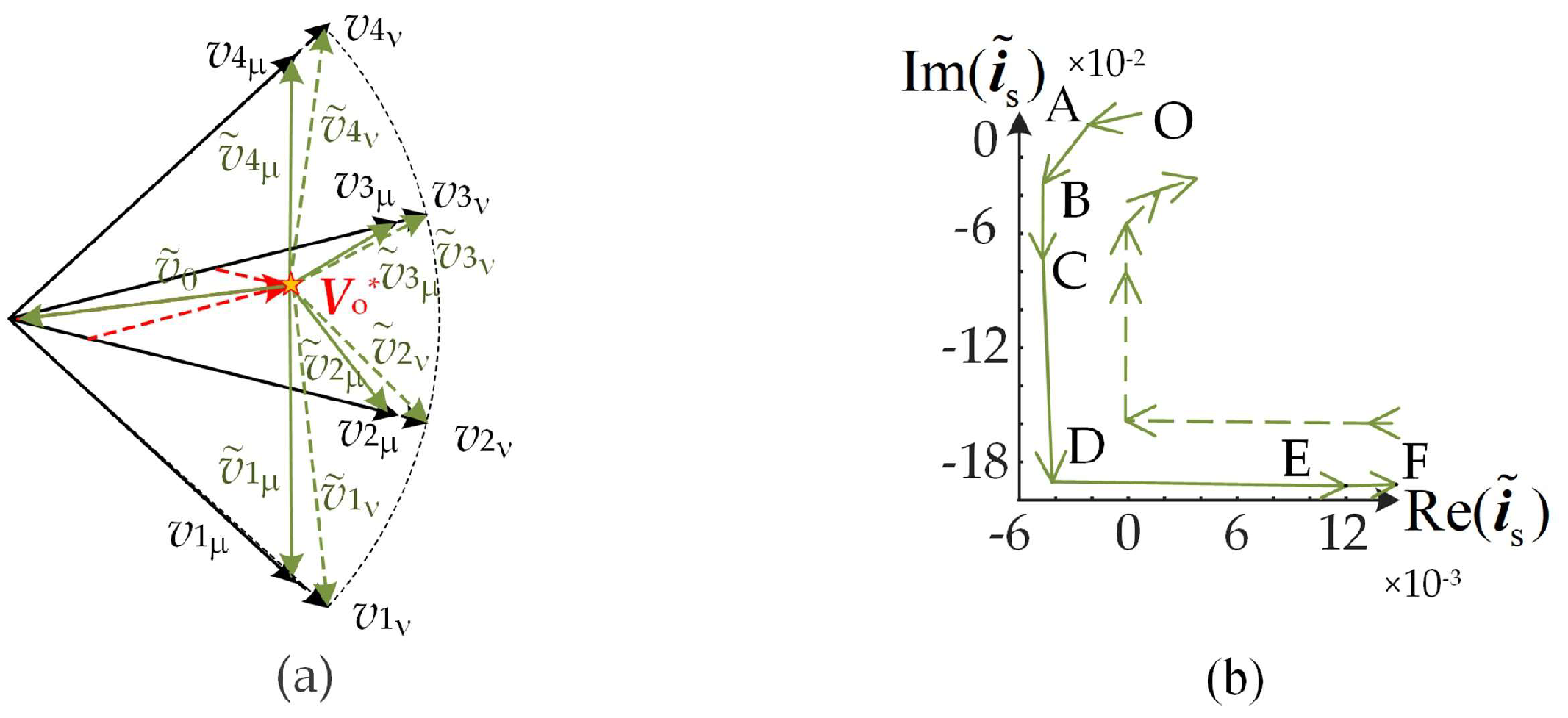
3.1. Output Voltage Error Locus

The equilibrium operating points of the vectors vs, is, vi, and ii are the grid voltage sampling value vector Vs, the average grid-side current vector Is, the average input voltage vector Vi, and the input-side current expectation vector Ii* per unit switching cycle. The disturbance signals are the ripple vectors v ˜ s , i ˜ s , and v ˜ i , and the input current error vector i ˜ i .
Space vector modulation utilizes fundamental voltage vectors and zero vectors to synthesize the continuously varying reference voltage Vo*. When there is a variance between the actual output voltage of the multiphase indirect matrix converter and the reference voltage, a vector model can be established to represent the error in voltage between the reference and actual output voltages [39,40].
V ˜ s ( t ) = v o V o *
where V ˜ s ( t ) represents the voltage fluctuation quantity, vo represents the actual output voltage vector, and Vo* is the reference voltage. Taking Vo* located in the first sector as an example, V1, V2, V3, and V4 are required to synthesize this vector, corresponding to inverter stages V55, V45, V44, and V64.
Taking Vo* located in the first sector as an example, V1, V2, V3, and V4 required to synthesize this vector correspond to the inverter levels V55, V45, V44, and V64, and the magnetic chain fluctuations will be presented as five dimensions in the unit switching period, which are v, v, v, v, v, v, and v, v, along the V1~V4. As shown in the PWM vector sequence, within one switching cycle, the actual input current vector is composed of five instantaneous vectors: the direction of iμα, iμβ along the direction of i1, and iνα, iνβ along the direction of i2, as well as the zero vector i0. Correspondingly, there are five types of error current vectors, as depicted in Figure 4a.
From this, the locus of the output current ripple vector is obtained, as shown in Figure 4b. At the beginning of the carrier cycle, t = t0, vo coincides with Vo*, and the voltage ripple vector corresponds to point O in Figure 4b; during the time period of t0~t7, the locus departs from point O and forms the polygon OABCDEFO along the direction of the arrow; from the vector sequence layout in Figure 2, it can be seen that the vector locus during the time period of t0~t7 is the same as that during the time period of t7~t14. It needs to be noted that the ratio of unit length on the Re-Im axis is set to 1:10, which is due to the fact that it is a qualitative rather than a quantitative calculation of ripples and does not mislead the understanding of its properties.

3.2. Small-Signal Model

Based on the principle of high-frequency synthesis, the space vector method employs a finite number of effective and zero vectors to continuously synthesize desired vectors with varying values. The discrepancy between the actual and desired vectors results in the input and output of the IMC containing numerous high-frequency voltage harmonics, ultimately contributing to the formation of high-frequency ripple components. It should be noted that Ii* is usually synthesized by the two boundary current vectors in the rectifier stage. In Figure 3, one section is the action time of the boundary current vector iμ, and the other sector is the action time of the boundary current vector iν. Thus, the chopper DC-link voltage of the multiphase IMC will be in a two-level fluctuation state along the three-phase sine envelope. This implies that the output current ripple of the IMC is not solely determined by the switching sequence of the inverter stage but is also affected by the switching sequence of the rectifier stage. In order to mitigate its impact on grid-side waveform quality, a second-order RLC low-pass filter is implemented at the input side to provide an independent low-impedance flow path for the ripple current. This facilitates the analysis of the output current ripple locus in relation to various factors such as output/input switching sequences and converter regulation system influence [41].
The input current of the IMC is generated by chopping the load current, resulting in a waveform characterized by a sequence of intermittent current pulses. To ensure the stability of the input voltage, a parallel filter capacitor Cf is required at the input terminal of the IMC. Furthermore, a series filter inductor Lf is necessary to attenuate the transmission of high-frequency harmonic components of the input current between the power supply and the IMC input. As a result, the high-frequency harmonic current primarily flows through the low-impedance path provided by Cf, which forms a loop and reduces its impact on the waveform quality of the source. Collectively, Cf, Lf, along with a damping resistor Rf, constitute the input filter. A single-phase equivalent circuit of the IMC system is shown in Figure 5, where the filter is a typical two-port network.
Using transfer functions, the following analysis is performed on the two-port network in the complex frequency domain of the s-plane: The source voltage vs. and the MC input-side current ii are selected as the independent variables of the port network; then, the source current is and the input-side voltage vi can be expressed using the hybrid parametric equation (h-equation) as follows:
v i s i s s = h 11 h 12 h 21 h 22 i i s v s s = h i i s v s s
The values of the elements of the hybrid parameter matrix h are as follows:
h 11 = v i s i i s v s s = 0 = 2 s R f L f s 2 R f L f C f + s L f + R f h 12 = v i s v s s i i s = 0 = s L f + R f s 2 R f L f C f + s L f + R f h 21 = i s s i i s v s s = 0 = h 12 h 22 = i s s v s s i i s = 0 = s L f + R f s C f s 2 R f L f C f + s L f + R f
where Lf, Cf, and Rf are the filter inductance, capacitance, and damping resistance, respectively.
Appropriate filter parameters are a prerequisite for the reliable operation of the IMC.
The input voltages iiA, iiB, and iiC result from the high-frequency modulation of the output current from the switching matrix. Furthermore, in the multiphase indirect matrix converter discussed in this paper, a low-pass filter is integrated between the input side and the grid side. This setup aims to curb the ingress of high-frequency harmonic components from the input current into the power grid. By doing so, it alleviates interference with other equipment at the common connection point and effectively filters out undesirable high-frequency harmonics.
The design of the filter necessitates careful consideration of its limitations and device selection criteria [30], which are evaluated based on the IMC equivalent circuit model illustrated in Figure 5. Initially, it is crucial to address the constraints regarding switching ripple and low-frequency harmonics. Since the fifth and seventh harmonics exhibit the highest amplitudes in the grid voltage, for simplification purposes, we will exclude the seventh harmonic from actual calculations. As depicted in Figure 5, the filter amplifies the harmonic component of the low-frequency voltage on the grid side. Therefore, it is imperative to restrict the low-frequency voltage gain coefficient of the filter to suppress low-frequency harmonics in the input voltage.
G j 7 ω b 2   dB
where wb represents the input fundamental angular frequency. Similarly, to effectively suppress the ripple component of the current carrier frequency on the grid side, it is necessary to adjust the current gain coefficient of the filter at the carrier angular frequency wc.
G j ω c 26   dB
Secondly, it is important to consider the limitations of inductor voltage drop and capacitor current. The ability to regulate the power factor is dependent on restricting the fundamental current of the filter capacitor. Therefore, it is crucial to take into account these limitations when designing the system for optimal performance.
I ω b   C f   v s 0.2 I i rated
where I i rated is the effective value of input current fundamental wave under rated load. To meet the voltage utilization requirements, it is necessary to limit the maximum fundamental voltage drop across the filtering inductance, under rated load conditions.
v ω b L f I 2 + I i rated 2 0.03 V s
where Vs is the RMS value of the gride-side voltage. At the same time,
I i rated = P i rated 3 V s = V o rated 2 R o 3 V s = 85   V 2 × 10   Ω 3 × 100   V 8.76   A
where P i rated is the rated active power, and V o rated is the RMS of the rated output voltage. From the above equation, the upper limit of the filter capacitance and inductance is as follows:
C f 55.8   μ F L f 1.09   mH
Finally, the damping resistance Rf is carefully chosen to prevent oscillation in the CL filter. It is crucial to limit the maximum power loss of the damping resistor Rf.
3 R f i R 2 0.01 P i rated
where iR is the filter resistor current. Based on the above analysis, the main performance indicators considered in the filter design process are determined according to the required parameters and comprehensive practical considerations as follows:
  • The attenuation ratio for high-order harmonics should be no less than 26 dB;
  • The gain of the seventh and lower-order harmonics must be limited to 2 dB;
  • The voltage drop in the inductor must not exceed 3% of the fundamental amplitude;
  • Reactive current flowing into the capacitor shall not exceed 20% of the rated current;
  • The loss on the Rf is less than 1% of the rated power.
Similarly, the output voltage vg and input current ii are chosen as the independent variables of the port network, and the output current ig and input voltage vi can be expressed using a mixed parameter equation (h-equation).
i g s v i s = h 11 h 12 h 21 h 22 i i s v g s = h i i s v g s
The values of the elements of the hybrid parameter matrix h are as follows:
h 11 = v i s i i s v s s = 0 = 2 s R f L f s 3 R f L f 2 C f + s 2 ( R f 2 L f C f + L f 2 ) + 2 s L f R f + R f 2 h 12 = v i s v s s i i s = 0 = 1 s L f + R f h 21 = i s s i i s v s s = 0 = 2 s R f L f s 2 R f L f C f + s L f + R f h 22 = i s s v s s i i s = 0 = 1 q

3.3. Current Ripple Model

As mentioned above, the SVM used in the IMC uses a limited number of active and zero vectors to generate a continuously changing target vector. The difference between the actual and targeted vectors results in the presence of numerous high-frequency harmonics in the input and output of the IMC. These harmonic components, which are filtered by the inductor/capacitor filter, manifest as output current ripples.
With the help of the Clarke transformation, the six-phase current quantities can be transformed into vector forms on the abc plane. The output current vector ig can be represented as follows:
i g = 2 3 1 1 e j 2 π / 3 e j 4 π / 3 e j π / 6 e j 5 π / 6 e j 3 π / 2 i A i B i C i U i V i W T
where iA, iB, iC, iU, iV, and iW are the six-phase current on the output side, and the superscript T denotes matrix transpose. Similarly, the output voltage vector vg, input current vector ii, and input current vector vi can be obtained. From this, it is easy to see that by generalizing the variables in (18) to vectors, the equation form remains unchanged.
Using small-signal analysis methods, the vector-expanded form of the nonlinear Equation (18) can be linearized. Thereafter, by defining small variations i ˜ g ( s ) = i g ( s ) I g ( s ) , v ˜ g ( s ) = v g ( s ) V g ( s ) , i ˜ i ( s ) = i i ( s ) I i ( s ) , and v ˜ i ( s ) = v i ( s ) V i ( s ) around equilibrium points Ig(s), Vg(s), Ii(s), and Vi(s), and assuming that the ripple of input current i ˜ i = 0 when the power supply is stable, it is possible to derive the small-signal model of the output side as follows:
i ˜ g ( s ) = 1 s L f + R f v ˜ g ( s )
Taking the inverse Laplace transform of (19), we can obtain the time-domain integral form of the output current ripple vector expression as follows:
i ˜ g ( s ) = 1 L f 0 t v ˜ g   d τ
Combined with the PWM switching sequence shown in Figure 3, the integration Equation (27) can be discretized as follows:
i ˜ g = 1 L f 0 t v ˜ g   d τ = i ˜ g , k + v ˜ g , k L f ( t t k 1 )
i ˜ g , k = i ˜ g , k + v ˜ g , k L f T k = n = 1 k v ˜ g ,   k L f T n
where k = 1, 2, …, 14, t ∈ (tk−1, tk) (indicated as O, A, B…in Figure 3), i ˜ g , k 1 is the output current ripple vector at t = tk−1 and i ˜ g , 0 = 0 ; v ˜ g , k is the output voltage error vector within (tk−1, tk); Tk = tktk−1.
The evaluation of the output current quality is typically conducted through quantification of the total harmonic distortion (THD). Nevertheless, the THD represents a frequency-domain metric that entails significant computational effort. The ripple constitutes a time-domain variable that incorporates all harmonic components of the output current. Consequently, the RMS value of the ripple signal can serve as an effective equivalent for characterizing the THD; that is, within a carrier cycle, the THD of the output current can be defined as follows:
T H D T c = 1 π 0 π i ˜ g , rms 2 d t i g fund × 100 %
where i g fund refers to the fundamental magnitude of the output current, and i ˜ g rms represents the RMS of output current ripple within unit carrier frequency cycle Tc, which is defined as follows:
i ˜ g , rms = i ˜ gA rms 2 + i ˜ gB rms 2 + i ˜ gC rms 2 + i ˜ gU rms 2 + i ˜ gV rms 2 + i ˜ gW rms 2
where i ˜ gA rms , i ˜ gB rms , i ˜ gC rms , i ˜ gU rms , i ˜ gV rms , and i ˜ gW rms denote the RMS of the six-phase source ripple currents. The maximum value of the ripple is limited to
i ˜ g , max = max O A , O B O F = max ( i ˜ g , k )
where max ( i ˜ g , k ) is the maximum value representing the output ripple vector, which is used to analyze the dynamic changes in the output current ripple locus.

3.4. Spread-Spectrum Modulation Based on Current Ripple Vectors

As depicted in Figure 4b, the locus of the output current ripple in the multiphase IMC is correlated with the amplitude and phase of the input–output voltages, among other factors. The fluctuation of the DC-link voltage vpn directly determines the output ripple vector. The carrier frequency based on the dynamic variation in the ripple locus no longer fluctuates within a specific range and has unique advantages in the spread spectrum. Matching high carrier frequencies in the high ripple range can expand the energy concentrated at specific frequencies to a wider spectrum, effectively reducing the THD. Simultaneously, matching low carrier frequencies in the low ripple range improves system efficiency while achieving the spread spectrum.
By combining the two principles mentioned above, the correspondence between the ripple locus and carrier frequency is further established. From (22), it can be seen that the length of each segment of the locus is only related to the carrier period Tc. It can be inferred that the scale of the ripple can be easily manipulated by modulating the carrier frequency. Therefore, in this section, by dynamically changing the carrier frequency with the ripple locus, the variation is no longer based on a fixed magnitude. This method aims to optimize the output spectrum and enhance system operational efficiency.
The variable Tc appears in each term of the ripple expression in (22). Hence, (25) can be rewritten as follows:
i ˜ g , max = max ( n = 1 k v ˜ g , k L f ) T n = max ( n = 1 k v ˜ g , k d n L f ) T c
where k = 1, 2, …, 14; dn = Tn/Tc. This demonstrates that the output current ripple is proportional to the carrier period Tc.
Within each carrier cycle, the carrier frequency is modified to maintain the modulation index i ˜ g , max at its specified value i ˜ g , max * . It is evident that the carrier frequency fc,carrier may be computed uniquely once the amplitude limit of the input voltage ripple vector in each cycle is known.
f c , carrier = max ( n = 1 k v ˜ g , k d n L f ) / i ˜ i ,   max * × 20   kHz
The RMS of the current ripple can be used in place of the THD as a standard indicator for assessing the quality of the current on the output side. Given that THD is a physical quantity that has been established over a long period of time, a suitable method must be used to assess if it complies with design criteria. In particular, it is sufficient to verify that the RMS of the output current ripple of any carrier period i ˜ g , rms satisfies the pertinent THD requirement after averaging over a certain time interval (typically equals to a fundamental period Tb).
T H D = 1 T b 0 T b i ˜ g , rms 2 d t i g rate
The traditional periodic PWM carrier frequencies fluctuate within a specific range. However, the carrier frequency defined by (19) no longer specifies a range of variation; instead, it dynamically adjusts with the trajectory of the ripple. This modification leads to a more standardized usage and eliminates the debugging process inherent in classical periodic PWM. It also facilitates clearer numerical indexes, thereby enhancing efficiency in carrier frequency fluctuation. Consequently, this approach can further reduce harmonic spikes near specific switching frequencies and promote a more uniform energy distribution within each frequency band.

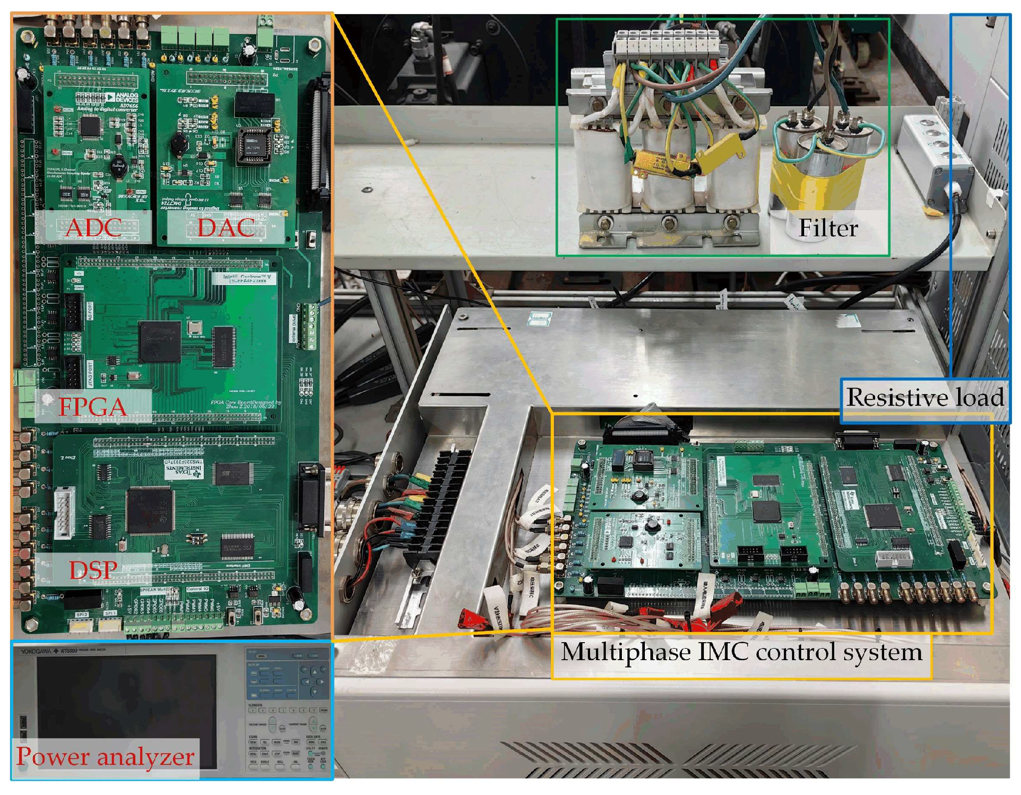
4. Experimental Results

To assess the impact and effectiveness of the proposed CR-SSM method in terms of spreading spectrum, enhancing power quality, and improving efficiency for multiphase IMC systems, a 3 × 6-phase IMC system prototype was utilized for simulation and experimental validation. Furthermore, to further confirm the efficacy of the proposed CR-SSM method, it was compared with various conventional periodic PWM strategies such as triangular (TWPWM), sinusoidal (SWPWM), and exponential (EWPWM) periodic PWM.
The experimental prototype of the IMC platform is shown in Figure 6. The controller was a DSP (TI F28379D) + FPGA (Intel 5CEFA4) architecture, where the SVM modulation algorithm was completed independently by FPGA. And DSP was used for the online calculation of the carrier frequency. The rectifier circuit consisted of six Infineon FF200R12KT3 power modules, while the inverter circuit included two two-level IPM modules PM25CLA120 from the MITSUBISHI. Measurement equipment such as oscilloscopes and power analyzers (WT5000) were all from the Yokogawa corporation, Tokyo, Japan. The specific system parameters are shown in Table 2.

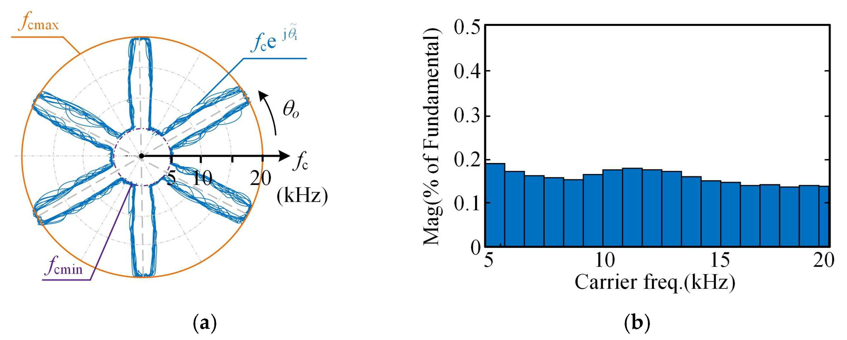
4.1. Analysis of Harmonic Suppression

To demonstrate the change in carrier frequency in terms of distribution characteristics, with respect to the input voltage phase angle θ ˜ i , the scalar value of fc was assigned the same phase information as θ ˜ i and converted to the vector form, i.e.,
f c = f c   e j θ i
The waveform of the vectorized carrier frequency fc can be represented using a polar coordinate system. In this system, the radial distance represents the value of the carrier frequency fc, and the angular coordinate represents the phase angle θ ˜ i of the input voltage vector. The orange and purple circles in Figure 7a, respectively, show the carrier frequency waveform for the CR-SSM method when fc = fc,max = 20 kHz and fc = fc,min = 5 kHz. The annular region between the two circles represents the feasible range of carrier frequency modulation. In order to visualize the distribution of the modulated carrier frequency in each frequency band, Figure 7b illustrates the histogram of the output harmonic distribution under the CR-SSM method in the 5–20 kHz band. The abscissa represents the harmonic frequency band, and it is divided into 17 equal segments to show the actual output of 5–20 k. The ordinate represents the approximate harmonic amplitude distribution in this band.
A comparison of three types of periodic PWM with the proposed CR-SSM method was performed for further evaluation of the effectiveness of the proposed method. The vectorized waveform of the frequency-modulated wave and the harmonic spectrum near 10 k for the other three types of periodic PWM methods are shown in Figure 8. The following observations can be made:
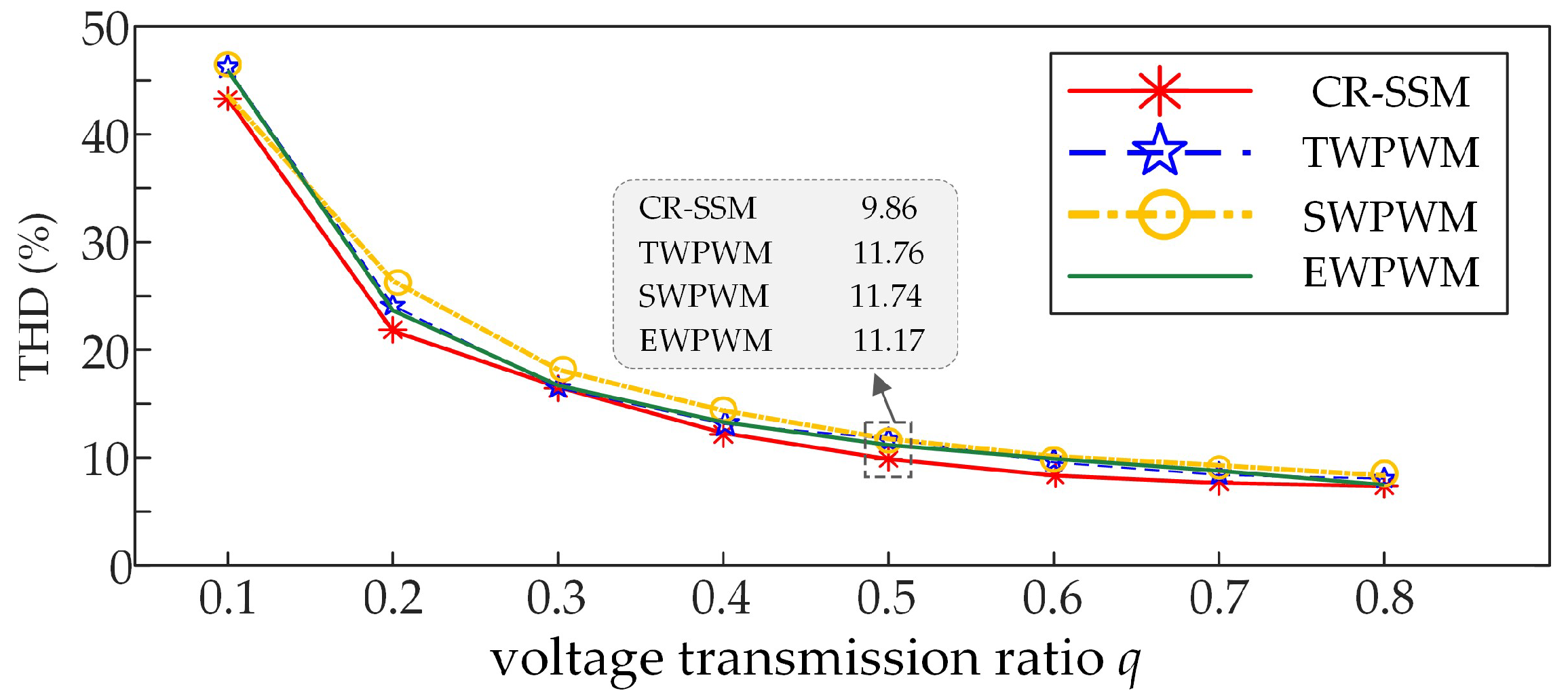
  • The strategy of periodic PWM to reduce the carrier frequency always results in a lower range of carrier frequencies compared to the CR-SSM method while maintaining the same limit on output current ripple. It can be seen that the classical periodic PWM still has harmonic spikes near the carrier frequency of 10 kHz, the variable band energy is still more concentrated, and the THD value is higher. The proposed CR-SSM method has better spectral characteristics, no harmonic spikes at specific frequencies, uniform high-frequency energy distribution, and better THD values.
  • The carrier frequency waveform displays periodicity along the direction of the output voltage vector angle θ ˜ o , but its locus is affected by the input frequency θ ˜ i , and it does fully coincide with the previous cycle after a complete cycle ( θ ˜ o = 2π).

4.2. Experimental Analysis of the Converter Efficiency

As the carrier frequency of the IMC system decreases, so do the losses. The efficiency of IMC can be improved by modulating the carrier frequency with CR-SSM, which employs a wider range of carrier frequency variations compared to the classical periodic PWM method. Therefore, it is necessary to conduct further experimental verification to determine the effect of CR-SSM and periodic PWM methods on the efficiency of IMC systems. Figure 9 shows the operational efficiency of the system under different methods. A comprehensive analysis of the data reveals the following observations:
  • The efficiency of the CR-SSM method is always lower than that of the periodic PWM method at different voltage transmission ratios q;
  • As the voltage transfer ratio q increases, the efficiency of the system also increases.
Figure 9 illustrates the three periodic PWMs (EWPWM, TWPWM, and SWPWM) and the operational efficiency of the multiphase IMC system under the proposed CS-SSM strategy. As depicted, the system efficiency of the CS-SSM method escalates from 27.5% to 94.5%; in SWPWM, it increases from 23.1% to 92.1%; in EWPWM, it increases from 23.3% to 91.9%; and in TWPWM, it increases from 22.8% to 92.2%. Notably, at modulation 0.8, the CR-SSM method boosts efficiency by 2.4%, 2.3%, and 2.6% compared to EWPWM, TWPWM, and SWPWM, respectively. Similarly, at modulation 0.6, the CR-SSM method enhances efficiency by 2.7%, 2.3%, and 2.9% compared to EWPWM, TWPWM, and SWPWM, respectively. The conjunction of these findings with Figure 9 demonstrates that the proposed CR-SSM method not only ensures a spread-spectrum effect but also enhances the operational efficiency of the multiphase IMC system by leveraging the carrier frequency density function based on the current ripple.

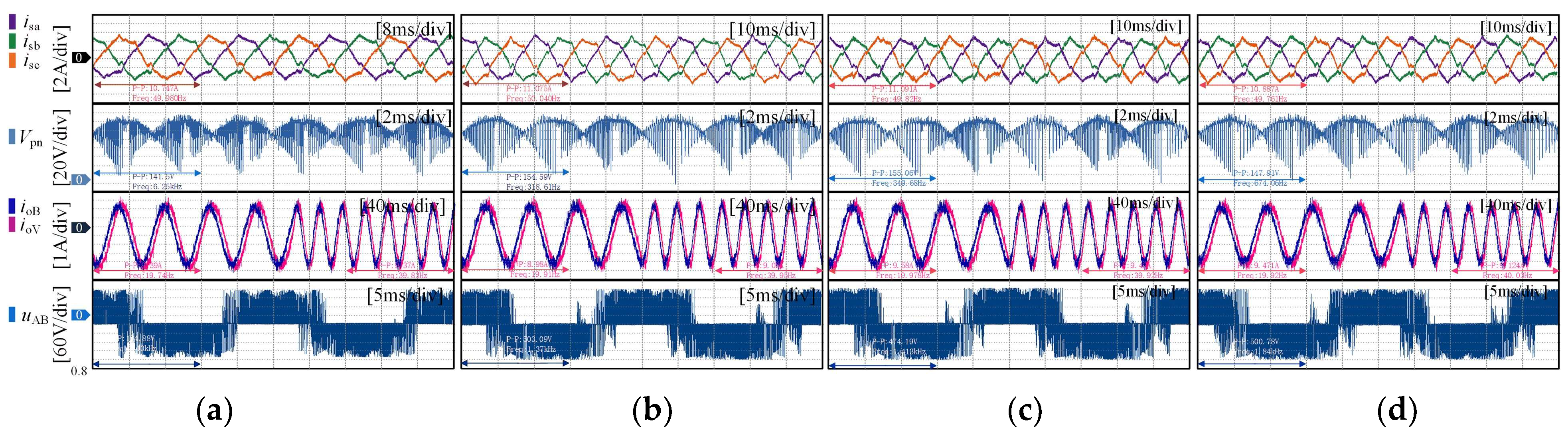
4.3. Experimental Results on Input–Output Waveform Quality

Figure 10 illustrates a comparison of the total harmonic distortion (THD) of load current under the CR-SSM method and periodic PWM. It can be observed that, under different voltage transfer ratio q conditions, the THD of the load current under the proposed CR-SSM method is lower than that of the periodic PWM method. This indicates that the carrier frequency modulation technique can effectively reduce the harmonic level of the IMC load current. Furthermore, as the modulation depth increases, the THD of the proposed CR-SSM is always lower than that of the periodic PWM method.
As depicted in Figure 10, the total harmonic distortion (THD) of the output current diminishes with increasing modulation. Notably, employing the proposed CR-SSM strategy results in a significant reduction in THD from 41.34% to 7.32%. Similarly, the THD for the TWPWM method decreases from 41.34% to 7.65%, while for the SWPWM method, it decreases from 43.09% to 7.89%, and for the EWPWM method, it decreases from 43.75% to 7.67%. At a modulation index of 0.5, the THD for CR-SSM is 9.86%, while for TWPWM, SWPWM, and EWPWM, it stands at 11.76%, 11.74%, and 11.17%, respectively. This trend underscores that, across all modulation methods, the THD of the proposed CR-SSM strategy remains consistently lower than the other three periodic PWM methods. The findings from Figure 4, Figure 5, Figure 6, Figure 7 and Figure 8 corroborate that the proposed CR-SSM strategy enhances the output current of the multiphase IMC system while ensuring the desired spread-spectrum effect.
The time-domain waveforms of the source current, DC-link voltage, input line voltage, and load current under various methods are shown in Figure 11. Figure 12 depicts the dynamic experimental waveforms using four different methods as the output frequency varies from 20 Hz to 40 Hz. It can be observed from Figure 11 and Figure 12 that the proposed CR-SSM method ensures a balanced sinusoidal three-phase source current, DC-link voltage, and load current without significant fluctuations. Moreover, it effectively suppresses harmonic amplitude at switching frequencies.

5. Conclusions

This study analyzes output current ripple to construct a carrier frequency density function and proposes a CR-SSM method suitable for multiphase IMC systems. The method selectively modulates carrier frequency without requiring changes to other modules, thus serving as a complementary tool to optimize PWM modulators like SVM and carrier modulation. CR-SSM utilizes output current ripple as an indicator to build a switch frequency density function, addressing the limitations of traditional periodic PWM in center frequency control. It offers a standardized application, eliminates the debugging process associated with classic periodic PWM, and defines clear numerical indicators. Additionally, it improves switch frequency efficiency, reducing harmoni2c peaks near specific switch frequencies. This promotes a more even energy distribution across frequency bands and optimizes system efficiency by correlating switch frequencies with output ripple heights. By distributing the power spectrum over a broader frequency range, the system’s output current spectrum is optimized. Experimental results demonstrate that compared to periodic PWM, the CR-SSM strategy effectively reduces system total harmonic distortion (THD) while enhancing operational efficiency in achieving spread-spectrum operation modes.

Author Contributions

Conceptualization, Z.Z.; data curation, L.X.; formal analysis, L.X.; funding acquisition, Z.Z.; investigation, C.L.; methodology, L.X.; project administration, Z.Z.; resources, Z.Z.; software, Z.Z.; supervision, Z.Z. and Q.G.; validation, L.X.; visualization, L.X.; writing—original draft preparation, L.X. All authors have read and agreed to the published version of the manuscript.

Funding

This research was funded by the “Zhejiang Provincial Natural Science Foundation of China under Grant No. LY24E070001”.

Data Availability Statement

The original contributions presented in the study are included in the article, further inquiries can be directed to the corresponding author.

Conflicts of Interest

The authors declare no conflicts of interest.

References

  1. Wang, R.; Lin, Z.; Du, J.; Wu, J.; He, X. Direct sequence spread spectrum-based PWM strategy for harmonic reduction and communication. IEEE Trans. Power Electron. 2016, 32, 4455–4465. [Google Scholar] [CrossRef]
  2. Raghuram, M.; Chauhan, A.K.; Singh, S.K. High-Gain-Integrated Switched Capacitor Indirect Matrix Converter. IEEE J. Emerg. Sel. Top. Power 2019, 3, 1846–1853. [Google Scholar] [CrossRef]
  3. Shi, T.; Wang, Z.; Ma, C.; Yan, Y.; Song, P. A Variable Switching Frequency PWM Method for Indirect Matrix Converters. In Proceedings of the 10th International Conference on Power Electronics, Machines and Drives (PEMD 2020), Online Conference, 15–17 December 2020; pp. 943–948. [Google Scholar]
  4. Padhee, V.; Sahoo, A.K.; Mohan, N. Modulation techniques for enhanced reduction in common-mode voltage and output voltage distortion in indirect matrix converters. IEEE Trans. Power Electron. 2016, 32, 8655–8670. [Google Scholar] [CrossRef]
  5. Nguyen, H.N.; Lee, H.H. An effective SVM method for matrix converters with a superior output perfor-mance. IEEE Trans. Ind. Electron. 2017, 65, 6948–6958. [Google Scholar] [CrossRef]
  6. Empringham, L.; Kolar, J.W.; Rodriguez, J.; Wheeler, P.W.; Clare, J.C. Technological Issues and Industrial Application of Matrix Converters: A Review. IEEE Trans. Ind. Electron. 2013, 60, 4260–4271. [Google Scholar] [CrossRef]
  7. Chen, J.; Sha, D.; Zhang, J. Current ripple prediction and DPWM-based variable carrier frequency control for full ZVS range three-phase inverter. IEEE Trans. Ind. Electron. 2020, 68, 1412–1422. [Google Scholar] [CrossRef]
  8. Casadei, D.; Serra, G.; Tani, A.; Zarri, L. Optimal use of zero vectors for minimizing the output current distortion in matrix converters. IEEE Trans. Ind. Electron. 2008, 56, 326–336. [Google Scholar] [CrossRef]
  9. Casadei, D.; Serra, G.; Tani, A.; Zarri, L. Theoretical and experimental analysis for the RMS current ripple minimization in induction motor drives controlled by SVM techniqu. IEEE Trans. Ind. Electron. 2004, 51, 1056–1065. [Google Scholar] [CrossRef]
  10. Attia, H.; Freddy, T.; Che, H.; Hew, W.; Elkhateb, A. Confined band variable carrier frequency pulse width modulation (CB-VSF PWM) for a single-phase inverter with an LCL filter. IEEE Trans. Power Electron. 2016, 32, 8593–8605. [Google Scholar] [CrossRef]
  11. Qin, X.; Zhou, B.; Wei, J.; Lei, J.; Liu, X.; Han, N. Distortion Analysis and Duty Ratio Correction Algorithm for Asymmetric Modulation of Two-Stage Matrix Converter. IEEE Trans. Ind. Electron. 2014, 62, 351–362. [Google Scholar] [CrossRef]
  12. Xie, L.; Ruan, X.; Zhu, H.; Lo, Y.-K. Common-Mode Voltage Cancellation for Reducing the Common-Mode Noise in DC–DC Converters. IEEE Trans. Ind. Electron. 2021, 5, 3887–3897. [Google Scholar] [CrossRef]
  13. Onederra, O.; Kortabarria, I.; De Alegria, I.M.; Andreu, J.; Gárate, J.I. Three-Phase VSI Optimal Switching Loss Reduction Using Variable Carrier frequency. IEEE Trans. Power Electron. 2016, 32, 6570–6576. [Google Scholar] [CrossRef]
  14. Marouani, K.; Baghli, L.; Hadiouche, D.; Kheloui, A.; Rezzoug, A. A New PWM Strategy Based on a 24-Sector Vector Space Decomposition for a Six-Phase VSI-Fed Dual Stator Induction Motor. IEEE Trans. Ind. Electron. 2008, 5, 1910–1920. [Google Scholar] [CrossRef]
  15. Gamoudi, R.; Elhak Chariag, D.; Sbita, L. A Review of Spread-Spectrum-Based PWM Techniques—A Novel Fast Digital Implementation. IEEE Trans. Power Electron. 2018, 12, 10292–10307. [Google Scholar] [CrossRef]
  16. Cano, J.M.; Navarro-Rodriguez, A.; Suarez, A.; Garcia, P. Variable Carrier frequency Control of Distributed Resources for Improved System Efficiency. IEEE Trans. 2018, 54, 4612–4620. [Google Scholar]
  17. Jamal, H.; Albatran, S.; Smadi, I. Variable carrier frequency algorithm for optimal tradeoff between switching losses and total demand distortion in grid-tied three-phase voltage-source inverter. In Proceedings of the 2016 IEEE Energy Conversion Congress and Exposition (ECCE), Milwaukee, WI, USA, 18–22 September 2016; IEEE: Piscataway, NJ, USA, 2016; pp. 1–7. [Google Scholar]
  18. Jiang, D.; Wang, F. Variable carrier frequency PWM for three-phase converters based on current ripple prediction. IEEE Trans. Power Electron. 2013, 28, 4951–4961. [Google Scholar] [CrossRef]
  19. Atamaniuk, V.; Kuznyetsov, O.; Lunkova, H. Driving the PWM-Controlled System to Monostable Behavior by Periodic Modulation of a Carrier Signal. In Proceedings of the 2022 IEEE 4th International Conference on Modern Electrical and Energy System (MEES), Kremenchuk, Ukraine, 20–22 October 2022; pp. 1–6. [Google Scholar]
  20. Shan, Y.; Pei, X.; Sun, T.; Zhang, M.; Zhou, P.; Jiang, D. Space spread-spectrum strategy for MMC to reduce the conducted EMI. IEEE Trans. Ind. Electron. 2021, 69, 10807–10818. [Google Scholar] [CrossRef]
  21. Chen, J.; Jiang, D.; Shen, Z.; Sun, W.; Fang, Z. Uniform distribution pulsewidth modulation strategy for three-phase converters to reduce conducted EMI and switching loss. IEEE Trans. Ind. Electron. 2019, 67, 6215–6226. [Google Scholar] [CrossRef]
  22. Li, Q.; Jiang, D.; Zhang, Y. Analysis and calculation of current ripple considering inductance saturation and its application to variable carrier frequency PWM. IEEE Trans. Ind. Electron. 2019, 34, 12262–12273. [Google Scholar]
  23. Chen, J.; Jiang, D.; Sun, W.; Shen, Z.; Zhang, Y. A Family of Spread-Spectrum Modulation Schemes Based on Distribution Characteristics to Reduce Conducted EMI for Power Electronics Converters. IEEE Trans. Ind. Applicat. 2020, 56, 5142–5157. [Google Scholar] [CrossRef]
  24. Le, D.; Choi, S. Network CM EMI Reduction Using Sinusoidal Frequency Modulated Carrier Wave Indexing. In Proceedings of the 2023 11th International Conference on Power Electronics and ECCE Asia (ICPE 2023-ECCE Asia), Jeju Island, Republic of Korea, 22–25 May 2023; Volume 38, pp. 3321–3326. [Google Scholar]
  25. Lumbreras, D.; Zaragoza, J.; Berbel, N.; Mon, J.; Gálvez, E.; Collado, A. Comprehensive Analysis of Hexagonal Sigma-Delta Modulations for Three-Phase High-Frequency VSC Based on Wide-Bandgap Semiconductors. IEEE Trans. Power Electron. 2021, 36, 7212–7222. [Google Scholar] [CrossRef]
  26. Menon, M.A.; Jacob, B. A New Space Vector Pulse Density Modulation Scheme for Two-Level Five Phase Induction Motor Drive. IEEE Trans. Ind. Electron. 2022, 69, 12077–12085. [Google Scholar]
  27. Huang, Y.; Xu, Y.; Zhang, W.; Zou, J. Modified Single-Edge SVPWM Technique to Reduce the Switching Losses and Increase PWM Harmonics Frequency for Three-Phase VSIs. IEEE Trans. Power Electron. 2020, 35, 10643–10653. [Google Scholar] [CrossRef]
  28. Ji, Z.; Cheng, S.; Li, X.; Lv, Y.; Wang, D. An Optimal Periodic Carrier Frequency PWM Scheme for Suppressing High-Frequency Vibrations of Permanent Magnet Synchronous Motors. IEEE Trans. Power Electron. 2023, 38, 13008–13018. [Google Scholar] [CrossRef]
  29. Ji, Z.; Cheng, S.; Ren, Q.; Li, X.; Lv, Y.; Wang, D. The Effects and Mechanisms of Periodic-Carrier-Frequency PWM on Vibrations of Multiphase Permanent Magnet Synchronous Motors. IEEE Trans. Power Electron. 2023, 38, 8696–8706. [Google Scholar] [CrossRef]
  30. Chen, N.; Yu, S.; Gao, L.; Huang, Y.; Chen, R. Suppressing Interference Peak in an Active Power Filter via Periodic Carrier Frequency Modulation Based on a Spectrum Analysis Approach. IEEE Trans. Electromagn. Compat. 2019, 61, 1760–1770. [Google Scholar] [CrossRef]
  31. Xu, J.; Nie, Z.; Zhu, J. Characterization and Selection of Probability Statistical Parameters in Random Slope PWM Based on Uniform Distribution. IEEE Trans. Power Electron. 2021, 1, 1184–1192. [Google Scholar] [CrossRef]
  32. Ma, Y.; Yang, M.; Lyu, Z.; Li, S.; Xu, D. Application of Periodic Carrier Frequency Modulation for Harmonic and EMI Reduction in GaN-Based Motor Drive. In Proceedings of the 2020 23rd International Conference on Electrical Machines and Systems (ICEMS), Hamamatsu, Japan, 24–27 November 2020; pp. 778–782. [Google Scholar]
  33. Nguyen, T.D.; Lee, H.-H. Dual Three-Phase Indirect Matrix Converter With Carrier-Based PWM Method. IEEE Trans. Power Electron. 2014, 2, 569–581. [Google Scholar] [CrossRef]
  34. Benson, M.; Dornala, A.; Andleeb, M.; Lee, K.; Lee, W. Simple and Robust Carrier-Based PWM Technique for Single-Stage Three-phase Rectifier Indirect Matrix Converter. In Proceedings of the 2024 IEEE Applied Power Electronics Conference and Exposition (APEC), Long Beach, CA, USA, 25–29 February 2024; pp. 691–697. [Google Scholar]
  35. Park, H.P.; Kim, M.; Jung, J.H. Spread spectrum technique to reduce EMI emission for an LLC resonant converter using a hybrid modulation method. IEEE Trans. Power Electron. 2017, 33, 3717–3721. [Google Scholar] [CrossRef]
  36. Dasgupta, A.; Sensarma, P. Filter design of direct matrix converter for synchronous applications. IEEE Trans. Ind. Electron. 2014, 61, 6483–6493. [Google Scholar] [CrossRef]
  37. Qiu, Z.; Chen, Y.; Kang, Y.; Liu, X.; Gu, F. Investigation into periodic signal-based dithering modulations for suppression sideband vibro-acoustics in PMSM used by electric vehicles. IEEE Trans. Energy Convers. 2020, 36, 1787–1796. [Google Scholar] [CrossRef]
  38. Leoncini, M.; Bertolini, A.; Melillo, P.; Gasparini, A.; Levantino, S.; Ghioni, M. Spread-spectrum frequency modulation in a DC/DC converter with time-based control. IEEE Trans. Power Electron. 2022, 38, 4207–4211. [Google Scholar] [CrossRef]
  39. Kumar, A.B.; Narayanan, G. Variable-Carrier frequency PWM Technique for Induction Motor Drive to Spread Acoustic Noise Spectrum with Reduced Current Ripple. IEEE Trans. Ind. Appl. 2016, 52, 3927–3938. [Google Scholar] [CrossRef]
  40. Li, Q.; Jiang, D. Variable Carrier frequency PWM Strategy of Two-Level Rectifier for DC-Link Voltage Ripple Control. IEEE Trans. Power Electron. 2017, 33, 7193–7202. [Google Scholar] [CrossRef]
  41. Xu, C.; Lu, S. Practical Online Modulation Method for Current Ripple and Switching Losses Reduction in the Three-Phase Voltage Source Inverters. IEEE Trans. Power Electron. 2021, 2, 1475–1490. [Google Scholar] [CrossRef]
Figure 1. A 3 × 6 IMC system.
Energies 17 02546 g001
Figure 2. The vectors diagram of 3 × 6 IMC drives: (a) rectifier stage; (b) α-β.
Energies 17 02546 g002
Figure 3. Switching pattern of 3 × 6 IMC.
Energies 17 02546 g003
Figure 4. Error vectors and their locus in the IMC output side in Section ①: (a) output voltage–error vectors. (b) output current ripple vectors.
Energies 17 02546 g004
Figure 5. A double-phase equivalent of the IMC system.
Energies 17 02546 g005
Figure 6. The experimental 3 × 6 IMC platform.
Energies 17 02546 g006
Figure 7. Plot of carrier frequency with CR-SSM of (a) vectorized waveform and (b) distribution histogram.
Energies 17 02546 g007
Figure 8. Comparison of the frequency variation locus between classic periodic PWM and CR-SSM switching method.
Energies 17 02546 g008
Figure 9. Operating efficiency of various methods under different working conditions.
Energies 17 02546 g009
Figure 10. THD comparison of CR-SSM and three classical periodic PWM methods.
Energies 17 02546 g010
Figure 11. Comparison between the proposed CR-SSM and classic periodic PWM: (a) CR-SSM; (b) TWPWM; (c) SWPWM; (d) EWPWM.
Energies 17 02546 g011
Figure 12. Comparison between the proposed CR-SSM and classic periodic PWM dynamics: (a) CR-SSM; (b) TWPWM; (c) SWPWM; (d) EWPWM.
Energies 17 02546 g012
Table 1. Voltage vectors and switch selection of the inverter sectors.
SecSecSecSecSecSec
V0000000000000
V2454426221311
V1554566263313
V7777777777777
V4646632335155
V3446422321151
V7777777777777
SecSecSecSecSecSec
V0000000000000
V1446422321151
V2646632335155
V7777777777777
V3662633135545
V4262213114544
V7777777777777
Table 2. Parameter settings.
ParametersSymbolValues
Effective value of grid-side phase voltage Vs100 V
Grid-side voltage frequencyfs50 Hz
Grid-side filter capacitorsCf35 μF
Grid-side filter inductorsLf1.37 mH
Grid-side filter resistorsRf10 Ω
Load resistance R10 Ω
Load inductance L30 mH
Output voltage frequencyfo20 Hz
Fixed carrier frequencyfc010 kHz
Disclaimer/Publisher’s Note: The statements, opinions and data contained in all publications are solely those of the individual author(s) and contributor(s) and not of MDPI and/or the editor(s). MDPI and/or the editor(s) disclaim responsibility for any injury to people or property resulting from any ideas, methods, instructions or products referred to in the content.

