Abstract
This paper investigates the behavior of SiC MOSFETs body diode reverse recovery as a function of different operating conditions. The knowledge of their effects is crucial to properly designing and driving power converters based on SiC devices, in order to optimize the MOSFETs commutations aiming at improving efficiency. Indeed, reverse recovery is a part of the switching transient, but it has a significant role due to its impact on recovery energy and charge. The set of different operating conditions has been properly chosen to prevent or force the snappy recovery of the device under testing. The experimental results and specific software simulations have revealed phenomena unknown in the literature. More specifically, the analysis of the reverse recovery charge, Qrr, revealed two unexpected phenomena at high temperatures: it decreased with increasing gate voltage; the higher the device threshold, the higher the Qrr. TCAD-Silvaco (ATLAS v. 5.29.0.C) simulations have shown that this is due to a displacement current flowing in the drift region due to the output capacitance voltage variation during commutation. From the analysis of the snappy recovery, it has emerged that there is a minimum forward current slope, below which the reverse recovery cannot be snappy, even for a high current level. Once this current slope is reached, Qrr varies with the forward current only.
1. Introduction
The body diode reverse recovery phenomenon is an important research topic [1,2,3,4,5,6,7,8,9,10,11,12,13,14], since its study is fundamental to improving the prediction of the performance of power converters adopting SiC MOSFETs. Indeed, the reverse recovery impacts the device switching speed and, as a consequence, the device operating voltage level due to the potential generation of over-voltages. Reverse recovery depends on a combination of factors related to the operating conditions such as DC-link voltage, load current, transient speed, and temperature, as well as on the MOSFET structure, which can be planar or trench. These operating conditions and the structure influence the occurring reverse recovery, which can be soft, hard or snappy [15]. Many studies compare the performance of Si and SiC MOSFETs [16,17,18,19,20,21,22,23,24,25,26,27,28,29]. Other studies have shown the response of the latter at varying operating conditions, such as gate-source voltage, temperature, drain current, current slope and so on [30,31,32,33,34,35,36,37,38,39,40,41,42]. However, the effects of the working conditions during snappy recovery have hardly been investigated and experimentally verified so far [43,44,45,46]. A double pulse test (DPT) with inductive load has been executed at different operating conditions to compare reverse recovery on different SiC MOSFET technologies: planar and trench [47,48]. The results show that the ringing and peak reverse current is highest in the planar SiC MOSFET, and the difference increases with increasing temperature. In both technologies, the reverse recovery shows a small dependency on the forward current and the blocking voltage. At high current, the body diode recovery performance of the planar SiC MOSFET is better than the trench one, since it presents a lower forward voltage (Vf).
In this paper, the analysis is focused on investigating the impacts of operating conditions variation on reverse recovery, and then on analyzing the limit conditions between the hard and snappy recovery of third-generation planar SiC MOSFET 750 V 11 mΩ devices made by STMicroelectronics in the HIP247-4L package. The paper contributes to increasing the knowledge about reverse recovery in SiC MOSFETs. More specifically, the measurements and TCAD simulations have revealed two unexpected phenomena at high temperatures. First, the reverse recovery charge, Qrr, decreases as the gate voltage increases. Moreover, the higher the threshold of the SiC MOSFET, the higher the Qrr. TCAD simulations have shown that the phenomenon is due to a displacement current flowing in the drift region due to the output capacitance voltage variation during commutation. An additional contribution is made by the deep analysis of the snappy recovery phenomenon, which has highlighted a set of conditions that the designer must consider in order to set or prevent its occurrence. Moreover, the experimental analysis has shown that below a given forward current slope, the snappy recovery phenomenon does not occur regardless of the current level. In particular, Qrr depends only on the forward current when the aforesaid current slope is forced. The paper is organized as follows. A brief description of the theoretical concepts regarding soft, hard and snappy recovery and the correlated issues are reported in Section 1. Section 2 recalls the basic concepts of reverse recovery for completeness, while Section 3 describes the experimental setup and reports some experimental results and TCAD simulations. Further results are reported in Section 4, which highlight the conditions for snappy recovery occurrence. Finally, the main conclusions are summarized in the last section.
2. Reverse Recovery Theoretical Concepts
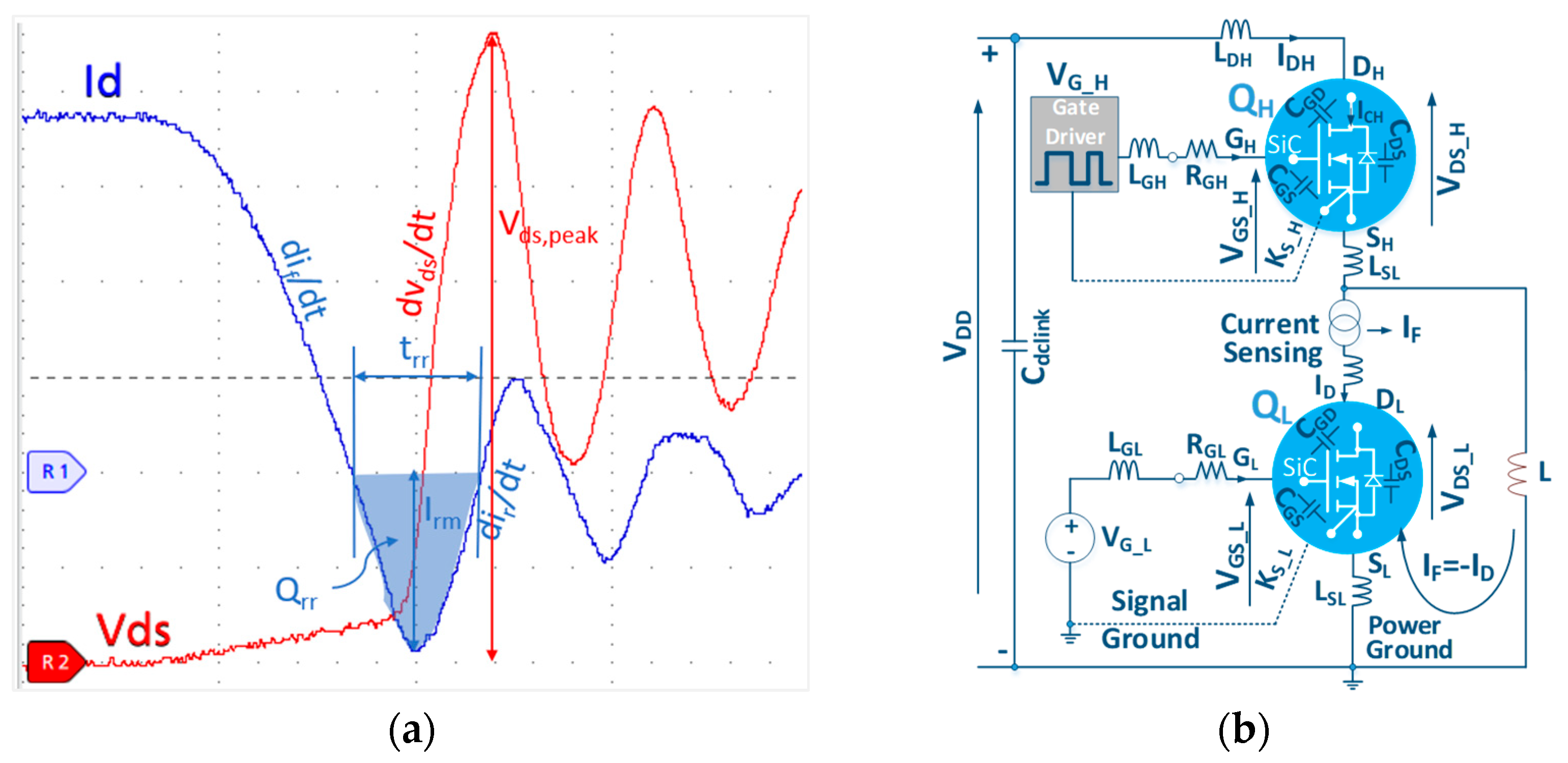
Reverse recovery occurs when the MOSFET body diode is switched off because of a positive voltage across device drain-source terminals (Vds). Before the switching-off, the charges in the drift region must be removed by a current that flows from the drain to the source, named the reverse recovery current [49]. Figure 1a shows an example of the body diode current and voltage during the switching-off and the quantities of interest that impact the reverse recovery analysis. The waveforms are obtained considering a classical half-bridge converter, as shown in Figure 1b.
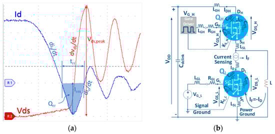
Figure 1.
Reverse recovery waveforms: (a) electrical signal and factors of interest, (b) equivalent electrical scheme of half-bridge configuration.
The body diode of the low side (LS) device begins the reverse recovery when the complementary one (high side device—HS) is turning on. Since the reverse recovery of the LS device is investigated, a negative constant voltage VG_L is applied to its gate through a gate resistance RGL to keep it off. On the contrary, the HS device is driven by a double pulse signal applied to its gate through a gate resistance RGH. In order to measure the reverse recovery current, a current sensor is placed in series with the device under test (DUT). The electrical scheme also reports all the parasitic inductances and capacitances of the devices responsible for overvoltages and oscillations, and consequently impacting device switching speed.
Of particular interest are the reverse current slope dir/dt and the forward current slope dif/dt, whose ratio (called snappiness factor, S) determines the kind of reverse recovery:
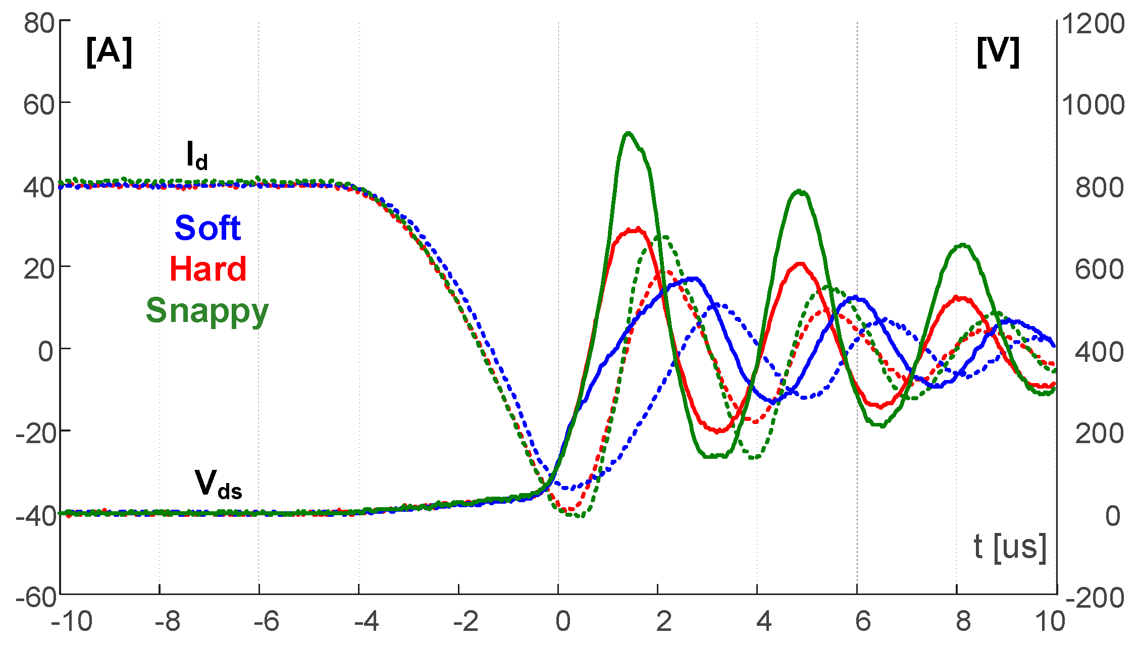
If S < 1, then the recovery is soft, else the recovery is hard, and when S is very high (S >> 1), the recovery is snappy (SR) [44]. Figure 2 reports the waveforms occurring in the three cases. The recovery is soft when the reverse current recovers to zero slowly and without oscillations impacting on the smooth rising of the drain-source voltage of the device working as a freewheeling diode. The recovery is hard when the current recovers to zero quickly, involving oscillations due to the resonant circuit formed by the stray circuit inductance and diode depletion layer capacitance. In this case, the diode reverse recovery can lead to serious voltage spikes. The recovery is snappy when these voltage spikes present an increment in the slope before reaching the peak. This increment is due to a faster charge removal. An experimental example of these three kinds of reverse recovery is reported in Figure 2.
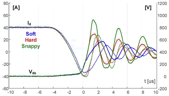
Figure 2.
Soft, hard and snappy recovery waveform examples.
How the current recovers to zero must always be investigated during device characterization, considering different parameters such as the forward current, the gate-source voltage, the temperature, and the forward and reverse slopes. This investigation is important in order to prevent oscillation and high voltage spikes that may lead to overpassing the breakdown voltage (BV) of the device.
Snappy recovery mainly occurs in SiC MOSFETs with high breakdown voltage (≥1700 V), which are designed to work at very high dc-link voltage, and consequently, very high drain-source voltage slopes could arise [44].
Three main factors mainly affect the SR. A factor is the junction capacitance, which depends on the MOSFET’s geometrical and process parameters. Another factor is the parasitic inductances of the power loop layout and the package of the converter. Finally, the switching speed also affects the SR. During the reverse recovery phase, the SR occurs if the free charges leave the junction before the current extinction. As a result, the current immediately “snaps” to 0. In this case, the interaction among the sudden change of current slope together with the layout’s parasitic elements and the diode’s depletion layer capacitance could lead to sustained voltage oscillations across the SiC MOSFET drain-source terminals [30,46].
3. Experimental Analysis and TCAD Simulation of Reverse Recovery
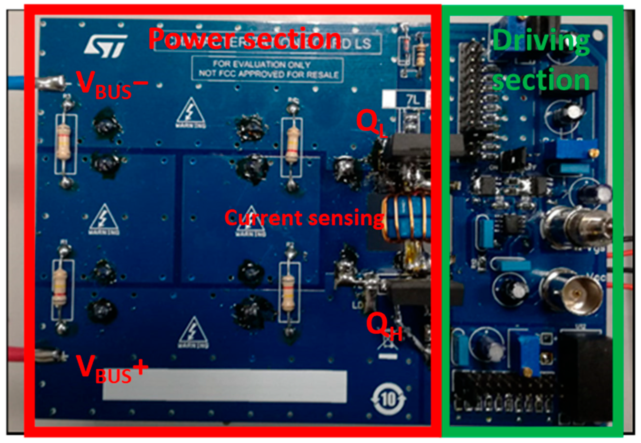
Figure 3 shows the characterization board used to analyze the reverse recovery, where the driving section and the power section are highlighted.
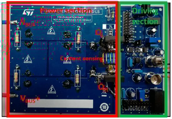
Figure 3.
Reverse recovery characterization board.
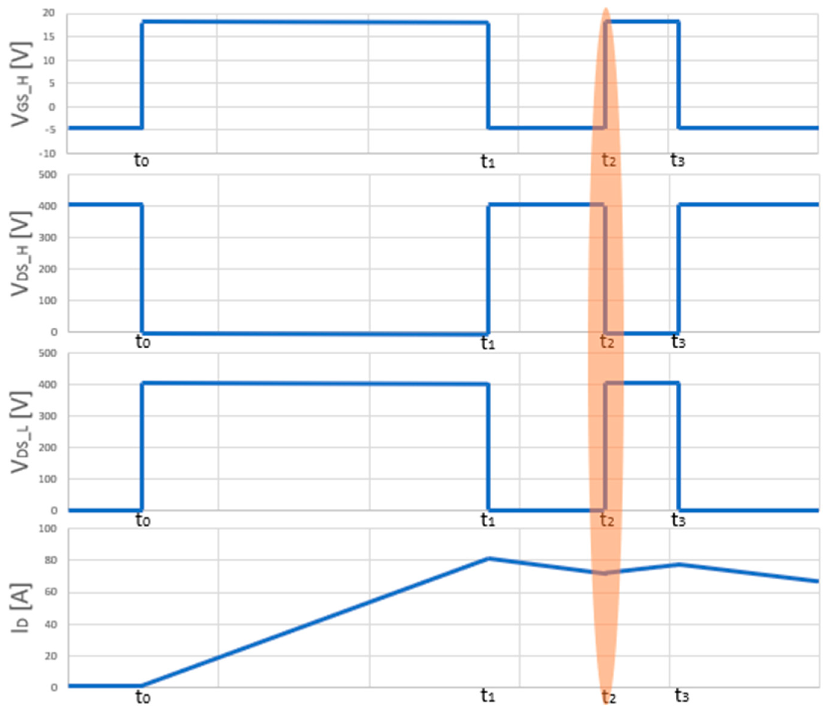
As reported in the electric scheme in Figure 2, the high-side device is used as a driver, and at its gate is applied a double pulse signal. The low side device is the DUT, and it is kept off by a negative voltage VG_L. Figure 4 shows the trends of double pulse test signals Vgs and Vds of the high-side MOSFET, the Vds of the low-side MOSFET and the load current. The front at which reverse recovery occurs is highlighted by the shaded orange area (t2). During the first pulse (t0–t1), the inductor L is charged. During the dead time between the two pulses (t1–t2), the inductor forces a current to flow through the body diode of the low-side MOSFET, and, in the rising edge of the second pulse (t2), a positive VDS_L is applied to the body diode, so its current decreases to zero and then flows in the opposite direction in order to carry out the charges stored in the drift region (reverse recovery current). The device used for this analysis is a Gen 3 750 V SiC MOSFET 11 mΩ. Three samples have been selected considering the distribution of static parameters among a sample of 200 devices. The devices under tests belong to three different values of threshold voltage, according to the statistical distribution reported in Figure 5. Considering that 50% of devices have Vth between 2.15 V and 2.25 V, this group has been considered to select the device (“Typ”) with typical Vth. The device (“Min”) with minimum Vth has been selected from the group 1.75 V–1.85 V, while the device (“Max”) with maximum Vth has been selected from the group 2.45 V–2.55 V. These three values of Vth have been chosen in order to investigate how parasitic turn-on (PTO) and snappy recovery (SR) are influenced by the threshold voltage of the device.

Figure 4.
Double pulse test.
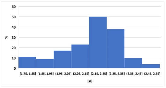
Figure 5.
Threshold voltage statistical distribution at 5 mA, 25 °C.
The aim of the experimental tests is the evaluation of the reverse recovery response by looking at the trend of the following recovery parameters (Figure 1a):
- Qrr reverse recovery charge;
- trr reverse recovery time;
- Irm negative peak current;
- Erec reverse recovery losses.
For each of the three devices, a set of measurements has been executed by varying three external operating settings:
- Temperature, Tc, (25 °C and 175 °C);
- Load current, Id, (40 A, 75 A and 120 A);
- Gate voltage, VG_L, (−8 V, −5 V, −3 V and 0 V).
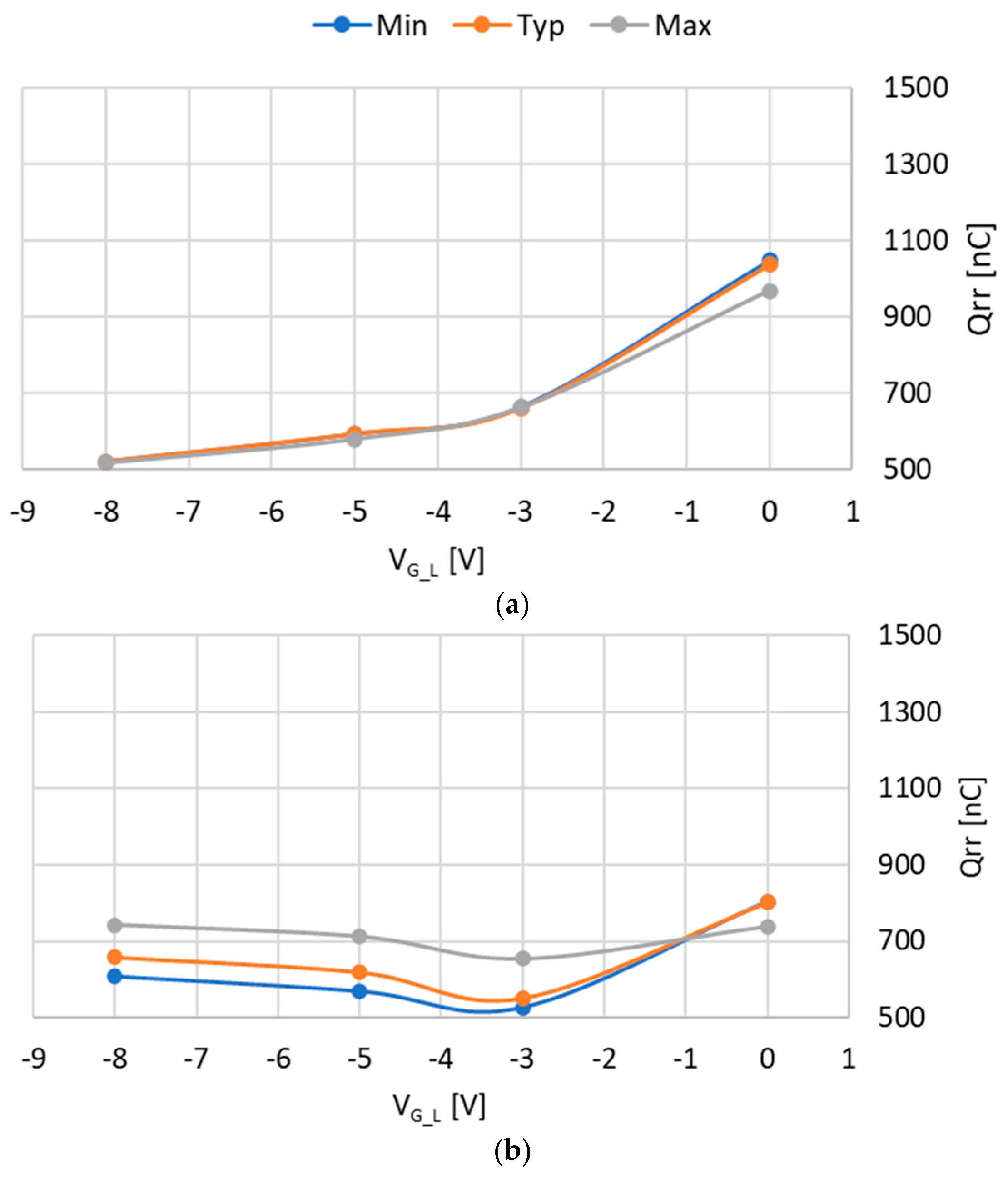
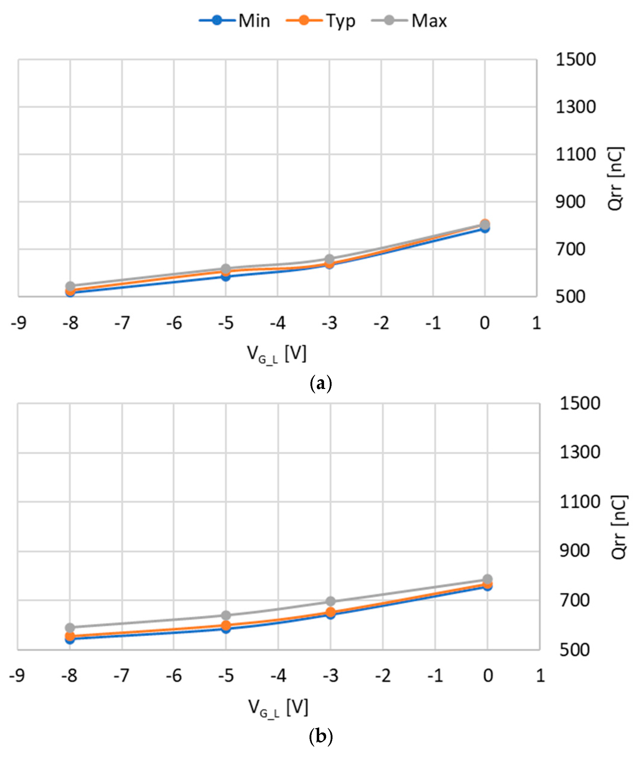
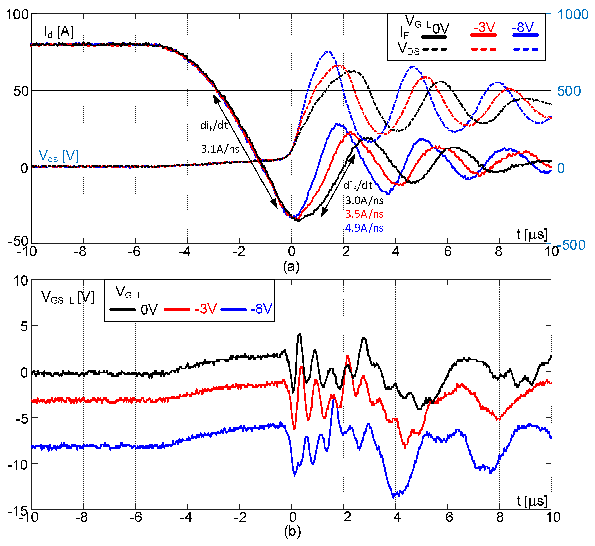
Since Qrr is the area of the current waveform during trr and it is also impacted by Irm, it is possible to summarize the reverse recovery performance by looking principally at Qrr. According to this, Figure 6 shows the reverse recovery charge as a function of VG_L at two different temperatures (25 °C and 175 °C) for the three devices, Min, Typ and Max, while keeping the current constant at 40 A. The DC bus voltage is set to 400 V and the current slope is regulated to around 2.5 A/ns. These tests verify that at 25 °C (Figure 6a), Qrr increases with the increment of VG_L. This behavior is expected at VG_L equal to zero, where PTO (parasitic turn-on) more easily occurs with a high injection of charges (coming from the channel) in the drift region, with a consequent increment of Qrr. For the case at VG_L equal to −8 V, PTO action can be excluded, and Qrr is basically related to minority carrier charges that at 25 °C have low average life time. On the contrary, at VG_L = 0 V, the operative conditions of the test (forward current and di/dt) lead to the injection of charges that are, in part, due to the PTO, which appears as though Qrr would be larger. The Qrr data for an intermediate value of VG_L, such as −3 V, experimentally show a different value of Qrr than the one at −8 V due to the non-ideal body-drain junction and drop voltage across parasitic inductors. Moreover, there is a different charge distribution due to the modulation of the depletion region next to the gate due to the different (negative) gate voltage. This means that in this intermediate case, due to the MOSFET structure, the combination of a limited injection of charges from the channel and the different charge distribution is responsible for an apparent Qrr increment. This behavior is confirmed by the waveforms shown in Figure 7 that highlight increased values of trr and Irm for higher VG_L levels. It is translated also in the form of a higher rising slope of the VDS_L as the VG_L is lower, since it is strictly correlated with the reverse recovery current slope.
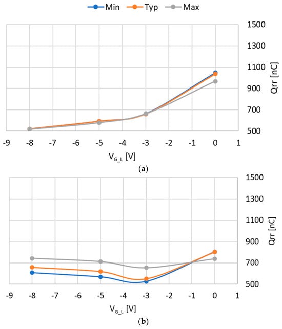
Figure 6.
Qrr vs. VG_L for the three devices, Min, Typ and Max, at 40 A, (a) 25 °C, (b) 175 °C.
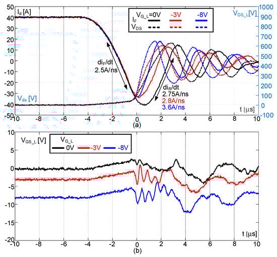
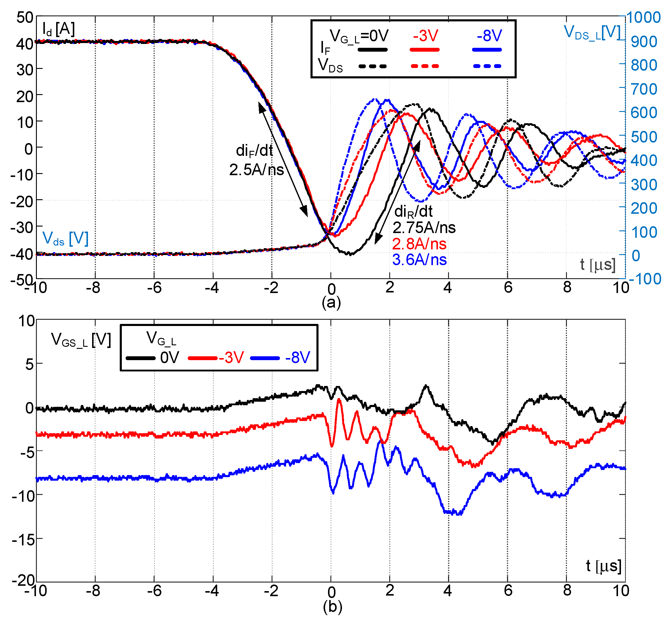
Figure 7.
(a) Id, Vds and (b) VGS_L of device “Typ” at 40 A, 25 °C, and different values of VG_L.
At 175 °C, Figure 6b, the average lifetime of minority carriers is longer, and consequently, this modifies the Qrr values and action of PTO according to VG_L values. Therefore, considering the working conditions adopted to evaluate the results reported in Figure 6a,b, the response of Qrr will be different because it depends on the temperature and VG_L value. Qrr shows a decrement from VG_L = −8 V to −3 V and then an increment from −3 V to 0 V. The most oscillatory recovery of the current waveforms at high temperatures reported in Figure 8 is amplified for lower values of VG_L (−8 V), causing a higher Irm compared to VG_L = −3 V and VG_L = 0 V. On the contrary, at VG_L = 0 V, the PTO causes a longer recovery time trr that determines a higher Qrr compared to VG_L = −8 V.
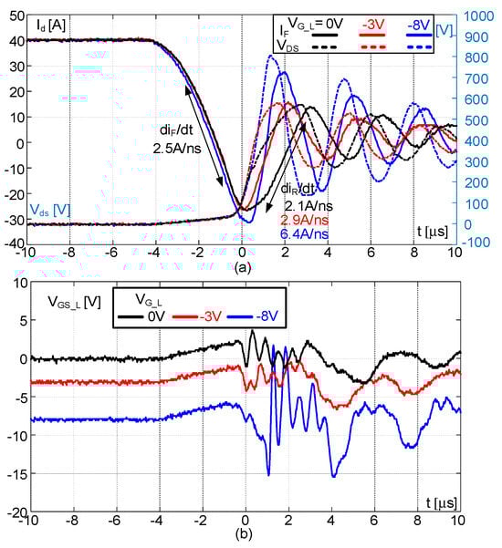
Figure 8.
(a) Id, Vds and (b) VGS_L of Typ at 40 A of forward current, 175 °C (junction temperature) and different values of VG_L.
Comparing Figure 6a,b, the most significant result is related to Qrr values at VG_L = 0, where Qrr is higher at 25 °C than 175 °C, despite VGS_L overvoltages being higher at 175 °C than 25 °C. This means that at high temperature, Qrr trends cannot be justified only by PTO. The Qrr reduction at 175 °C and VG_L = 0 is reasonable, since Irm here is also lower than the case at 25 °C (−40 A at 25 °C and −25 A at 175 °C).
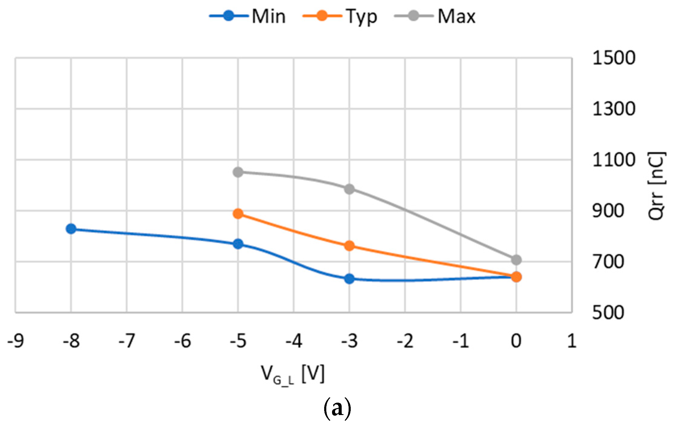
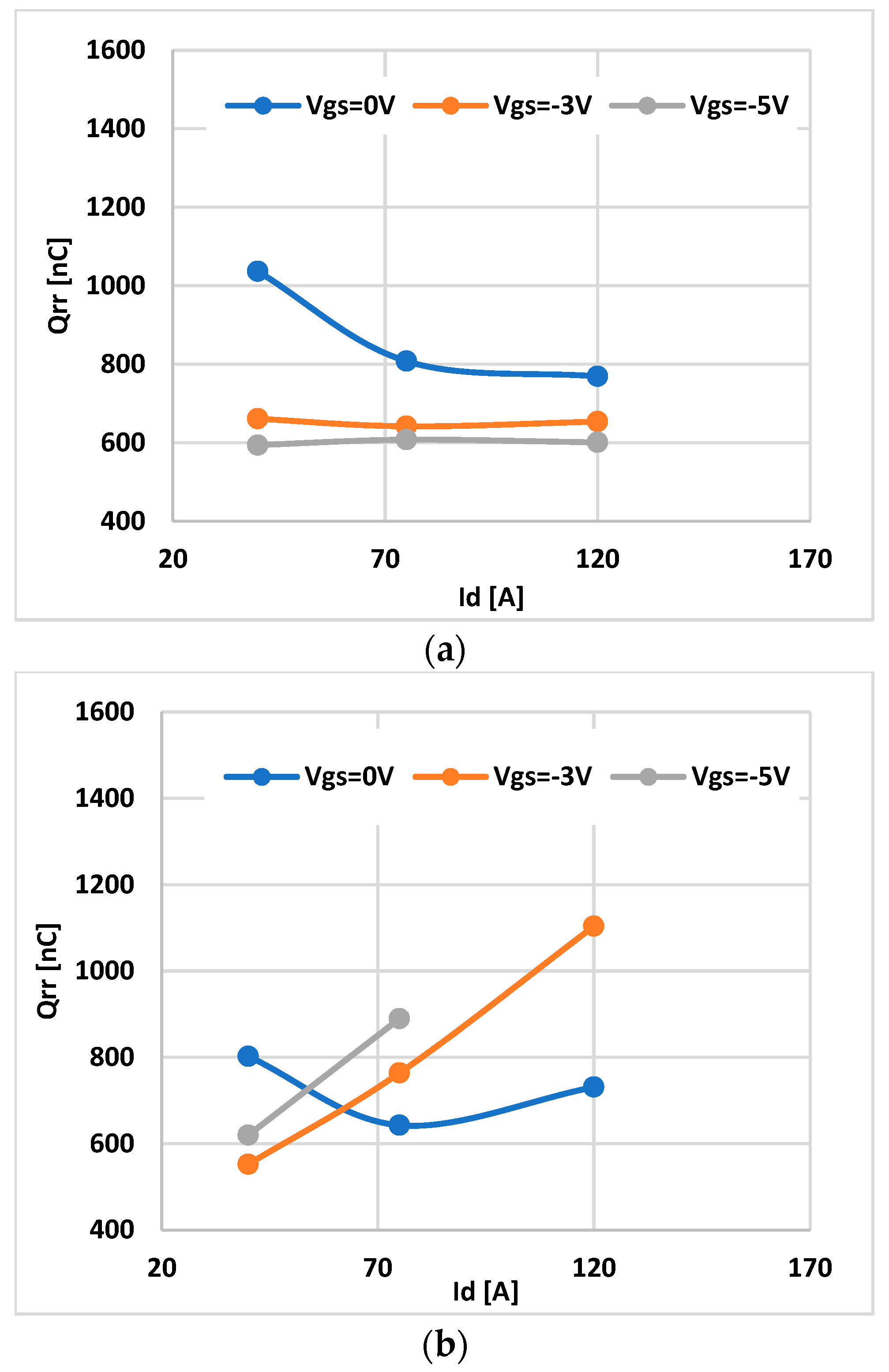
The reverse recovery response, inferred from the Qrr trendline at 25 °C, 40 A, in Figure 6a, is also confirmed at high currents, as verified by the results illustrated in Figure 9a,b, respectively, at 75 A and 120 A for the same devices under test: “Min”, “Typ” and “Max”. The Qrr in these two cases varies from 500 nC (VG_L = −8 V) to 800 nC (VG_L = 0 V) against the variation observed at 40 A, where it reaches a value of 1000 nC (VG_L = 0 V).
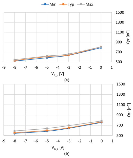
Figure 9.
Qrr vs. VG_L for the three devices Min, Typ and Max at 25 °C, (a) 75 A, (b) 120 A.
In this structure, with a high current, the drift region is more quickly emptied than in the low-current case. Indeed, by comparing the waveforms of Figure 7a and Figure 10a, the higher the forward current, the higher the reverse recovery current slope (dir/dt).
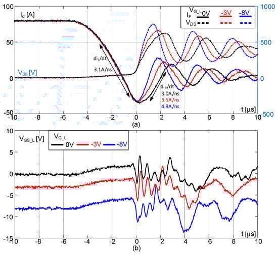
Figure 10.
(a) Id, Vds and (b) VGS_L of device “Typ” at 75 A of forward current, 25 °C and different values of VG_L.
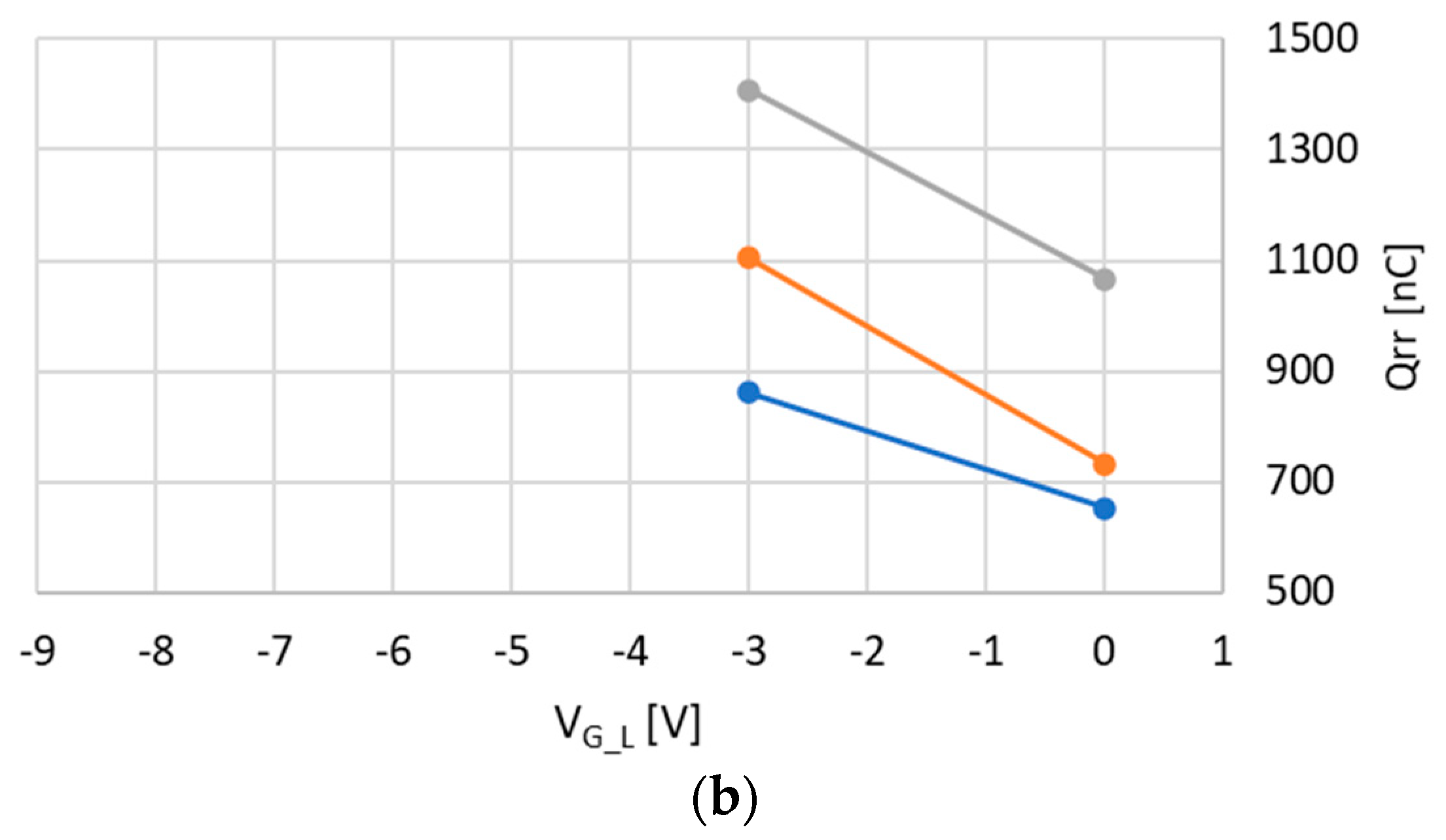
Figure 11 shows an opposite trend of Qrr vs. VG_L for the three devices Min, Typ and Max, compared to Figure 9, evaluated only by changing the temperature to 175 °C. In fact, at this temperature, Qrr decreases with the increment of VG_L. It is an unexpected behavior, and in order to understand it, some simulations based on TCAD-Silvaco have been executed. The results related to some working conditions are not reported because they have not been executed to avoid a drain-source voltage overshoot exceeding the breakdown voltage.
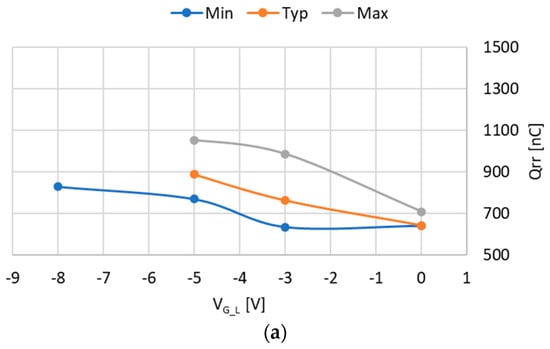
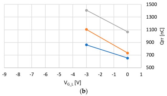
Figure 11.
Qrr vs. VG_L at 175 °C for three devices Min, Typ and Max for different values of forward current. (a) 75 A (b) 120 A.
Figure 12 reports Qrr as a function of the forward current at different VG_L and temperature values for device “Typ”. The temperature influences the average lifetime of minority carriers and, consequently, drastically changes the Qrr trendline, providing very different response depending on the operative conditions.
Figure 12.
Qrr vs. forward current for “Typ” device for different values of VG_L at (a) 25 °C, (b) 175 °C.
To support and better understand the mechanism of reverse recovery of the device under test, the half-bridge configuration has been developed in TCAD-Silvaco software, and the electrical parameters of the devices used to set the model are included in Table 1. The physics model used in the simulation was the Schottky–Read–Hall (SRH), for recombination, bandgap narrowing, incomplete ionization of the dopant, the ATLCVT mobility model and anisotropic impact ionization (IMPACT ANISO). The material specification of 4H-SiC and dielectric properties are reported in the ATLAS SILVACO manual (Silvaco International (2015) ATLAS User’s Manual Device Simulation Software Silvaco International, Santa Clara), and some of those used in this model are reported in Table 1.

Table 1.
Material specifications for 4H-SiC, ATLAS SILVACO manual.
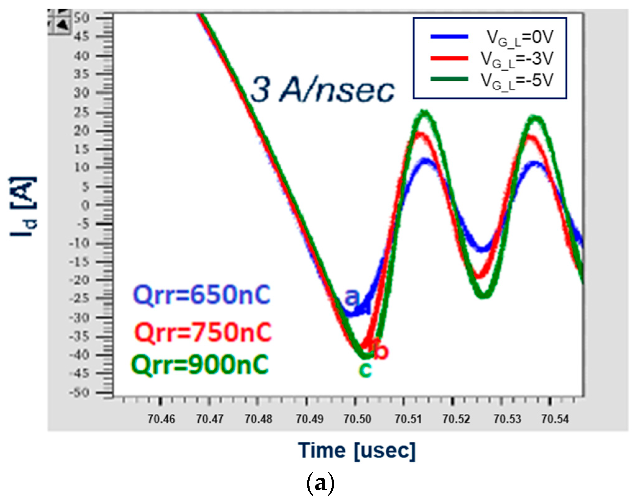
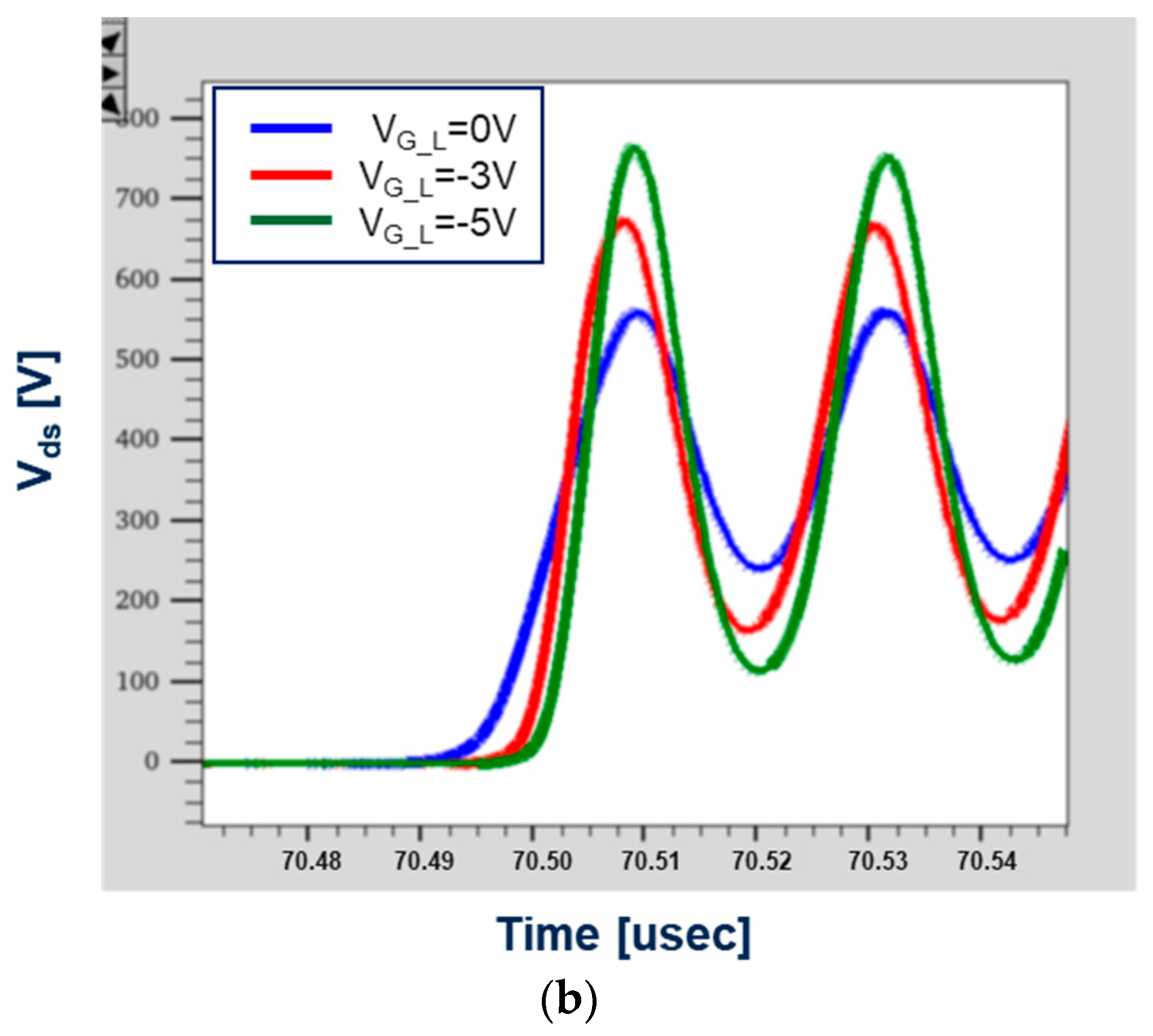
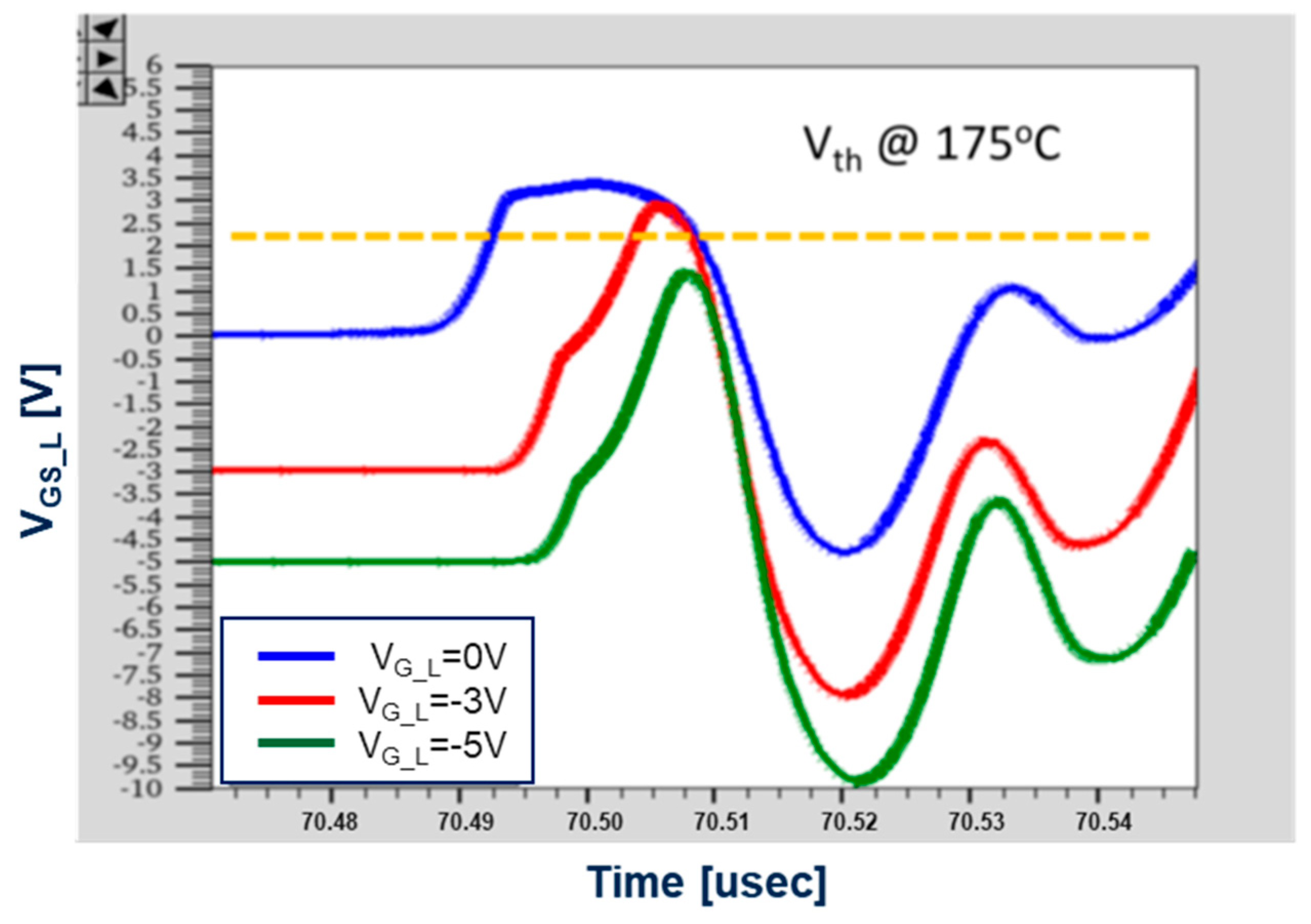
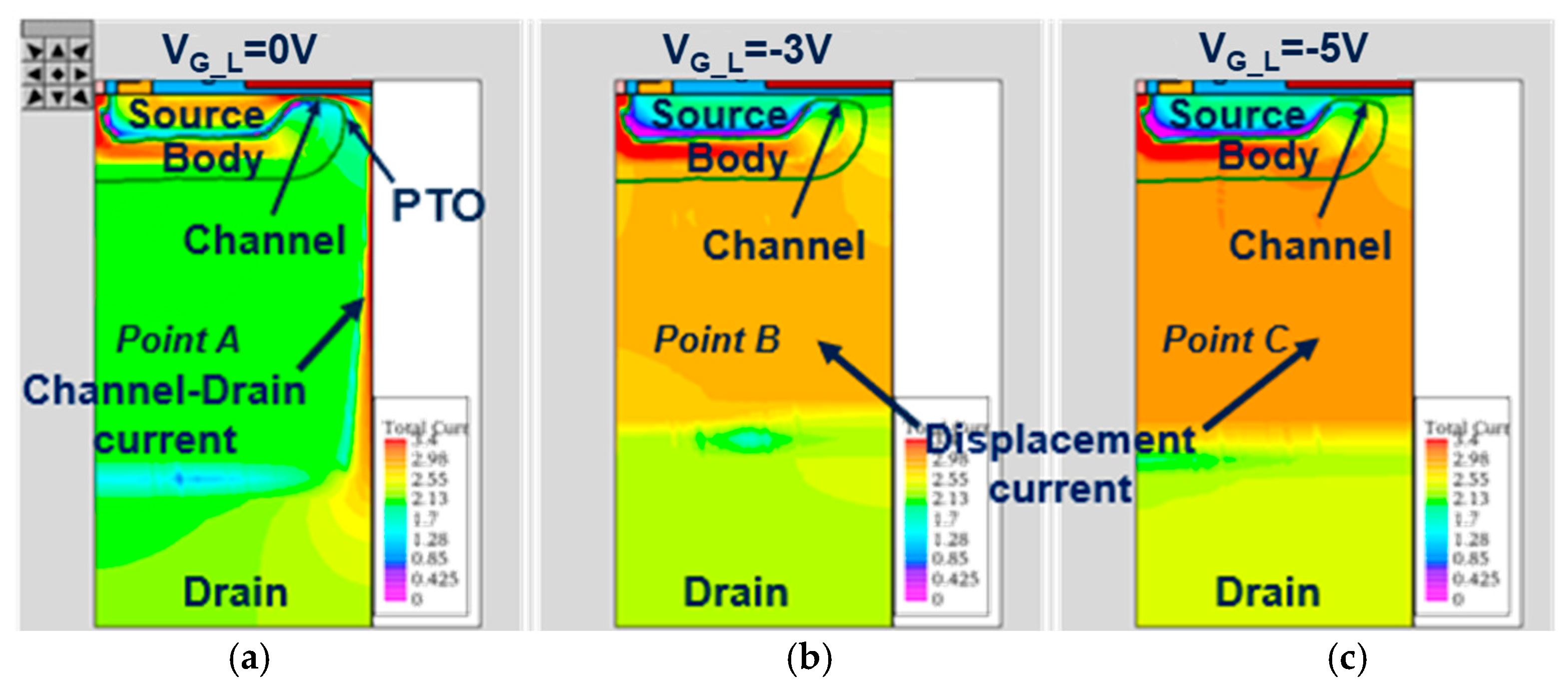
Figure 13a reports the magnification of the simulated body diode current (at 75 A) and Figure 13b reports the simulated Vds voltage for VG_L = 0 V, −3 V and −5 V at Tj = 175 °C. Figure 14 shows the gate-source voltage of the device operating as a freewheeling diode. The TCAD simulations confirm that Qrr decreases from 900 nC to 650 nC; hence, the higher the VG_L (shown in Figure 11), the lower Qrr. This happens despite the VG_L peak voltage, measured in correspondence with the maximum negative peak of the current Irm (points a, b and c in Figure 13a), overpassing the threshold voltage for a period sufficient to cause a PTO in the worst case (i.e., VG_L = 0 V). In addition, the color maps of the current density (Figure 15) (related to the maximum negative peak of Irm shown in Figure 13a) also confirm that there is a higher current density in the drift region when VG_L = −3 V and VG_L = −5 V than when VG_L = 0 V. This counterintuitive behavior of the current density in Figure 15b,c is due to a displacement current, which flows in the drift region due to the variation of the parasitic output capacitance voltage during the commutation of the high-side device. This current causes an increment of charges in the drift region and, consequently, a higher Qrr with respect to the case at VG_L = 0 V. It is also worth noting that the device with a higher threshold voltage (Max) presents the highest Qrr, as evident from Figure 11.
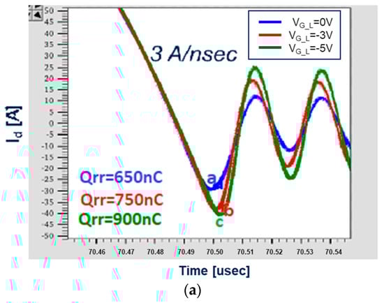
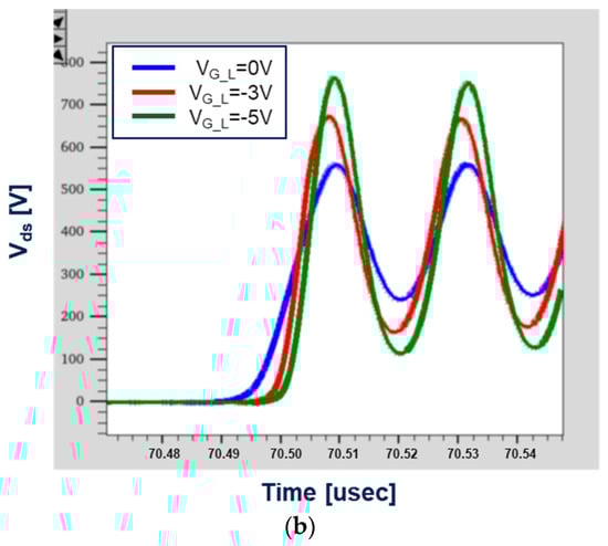
Figure 13.
Body diode (a) current and (b) voltage for VG_L = 0 V, VG_L = −3 and VG_L = −5 V simulated with TCAD (at 75 A).
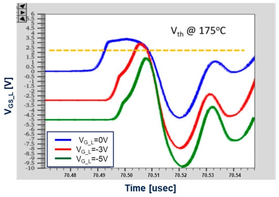
Figure 14.
Instantaneous gate-source voltage of DUT during turning on of the complementary device.
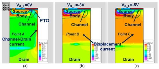
Figure 15.
Current density color map [A/cm2] in logarithmic scale during commutation for (a) VG_L = 0, (b) VG_L = −3 V and (c) VG_L = −5 V relative to the minimum current value of Figure 13a, indicated with “a”, “b”, “c”.
To sum up, the experimental results and TCAD simulations demonstrate that there is not a unique response of the intrinsic body diode during reverse recovery. Considering the operating conditions related to VDD and dif/dt, it is possible to separate the behavior at the low current, with VG_L changing from −8 V to 0 V (where Qrr increases at low temperatures (25 °C) and high temperatures (175 °C)), from the behavior at high current. In this last case, at a low temperature, Qrr increases when VG_L moves from −8 V to 0 V, while, at a high temperature, it decreases despite the possible effect related to the triggering of PTO, especially at VG_L = 0. However, the worsening of the operative conditions, in terms of forward current level and temperature, does not impart reverse recovery with a strong oscillatory behavior; instead, it is possible to see VDS voltage waveforms with limited oscillations.
4. Analysis of Snappy Recovery Limits
In this section, we investigate the reverse recovery response when the extremization of the operative conditions is responsible for the generation of significant drain-source overvoltage. This behavior is usually called “snappy recovery” [44].
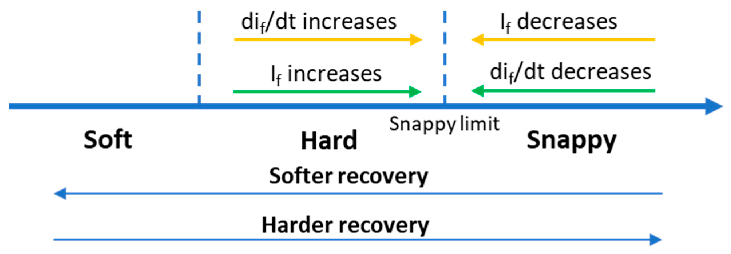
It is desirable to have fast recovery, and this can be achieved with a high current and voltage slope. However, in this case, the reverse recovery will belong to the “hard” type, as indicated in the JEDEC standard [15]. Unlike soft recovery, where voltage and current profiles do not present significant overvoltage and/or overcurrent, in this case, oscillatory behavior during the recovery is expected. The hard recovery can become snappy for specific values of forward current, slope, temperature or VG_L. Hence, it is useful to change these operating conditions to identify when this phenomenon is triggered. A representation of this occurrence has been illustrated in Figure 16.
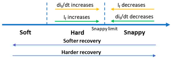
Figure 16.
Identification of “snappy limit condition”.
To find the conditions leading to snappy recovery (snappy limit defined in Figure 16), dedicated measurements have been executed for the DUT, at different values of:
- -
- Temperature (175 °C and 200 °C);
- -
- Gate-source voltage (−5 V and −8 V).
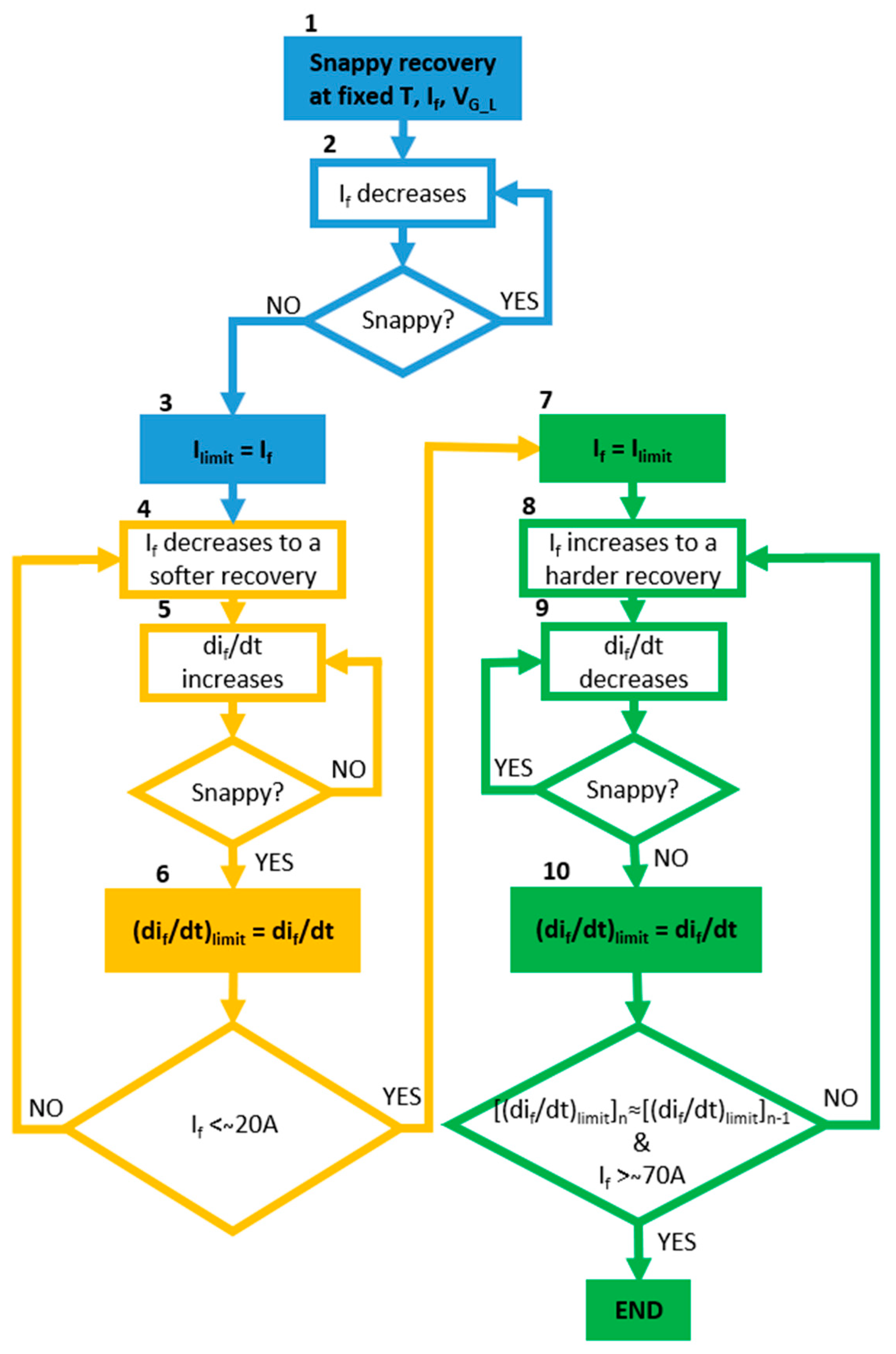
The procedure is reported in the flow chart of Figure 17. Starting from a condition of Tj, If and VG_L where the recovery is surely snappy (point 1), the forward current is decreased (point 2) until the snappy recovery is maintained. Once a current value that precludes snappy recovery is found, this value represents the limit current, set as Ilimit (point 3), which determines a limit condition between hard and snappy recovery. It is worth noticing that dif/dt is lower than at the beginning. Starting from this value of current, Ilimit (where the recovery is hard), the forward current is reduced until a softer recovery is reached (point 4), hence the dif/dt is a little reduced. Therefore, the dif/dt that is set by the active device is increased (point 5) by changing its gate resistance, to come back again to the limit between the hard and snappy recovery. The dif/dt at which this occurs is the (dif/dt)limit (point 6). The snappy recovery boundary is asymptotically reached by considering forward current reduction and increasing of dif/dt. This procedure is iterated until If reaches low values (set to about 20 A for this device), at which an even higher dif/dt cannot trigger snappy recovery. Once the iteration is concluded, the forward current is set to the Ilimit value (point 7) found in point 3, and the process is repeated by increasing the value of If (point 8), moving to a harder recovery. Hence, the dif/dt is decreased (point 9) to reach again the limit between hard and snappy recovery (point 10). This process is iterated as long as the gap between the (dif/dt)limit at the n iteration is almost equal to the (dif/dt)limit at the n − 1 iteration. However, the process is interrupted if a high current is reached (set to about 70 A for this device) to avoid stressing the device.
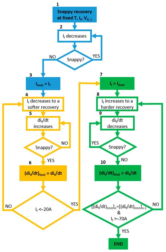
Figure 17.
Snappy limit flow chart.
The research process of determining the snappy recovery limit condition and the relation between Ilimit and dif/dt can be repeated by varying the temperature and the gate-source voltage of the device used as a freewheeling diode. The experimental results derived to study this behavior have been collected for the three devices (Min, Typ, Max) under test, considering the most stressful temperatures 175 °C and 200 °C and VG_L = −8 V and −5 V, since these operating conditions can easily trigger snappy recovery.
According to the aforementioned procedure, we establish the current values Id where the devices operate in snappy recovery, and these are reported in Table 2. From these values, we take Ilimit as the starting point of the research process of snappy recovery limit conditions. The experimental application of the algorithm shown in Figure 17 has allowed us to identify the dif/dt that determines the snappy limit conditions (associated with a specific Ilimit current value), which can be correlated to reverse recovery charge Qrr.
Table 2.
Limit current between hard and snappy recovery at different conditions of Vth, VG_L, Tj and Id.
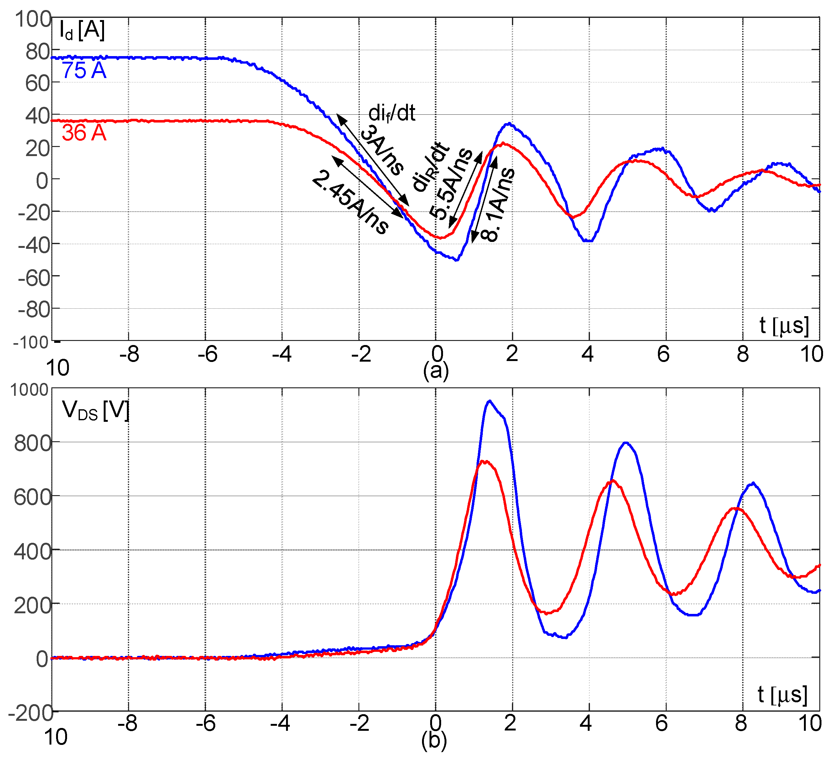
Figure 18 shows the Id and Vds waveforms of the Min at Tj = 175 °C, and VG_L= −8 V at the starting current Id = 75 A, where the device operates in snappy recovery, as well as the limit current Ilimit = 36 A where the recovery is no longer snappy. Figure 19 shows a set of curves of Qrr trend vs. dif/dt for different combinations of VG_L and Tj values for the three devices (a) Min, (b) Typ and (c) Max. According to the flow chart of Figure 17, the increasing dif/dt and consequently decreasing If are correlated with the applications of the procedure described in points 3-4-5-6, while the snappy limit conditions where dif/dt decreases and If increases correspond to the application of points 7-8-9-10 of the aforementioned flow chart. It is important to note that each point of the curves of Qrr with respect to dif/dt is obtained at a different value of forward current, since they are points that define the limit condition for snappy recovery. In particular, the higher the dif/dt, the lower the If. The procedure described in the flow chart is applied in Figure 19 when VG_L = −8 V/Tc = 175 °C and VG_L = −8 V/Tc = 200 °C. When VG_L = −5 V/Tc = 175 °C, it is not possible to reach the snappy condition at a low value of current because it requires a too-high dif/dt.
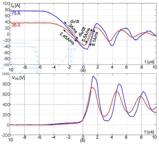
Figure 18.
(a) If and (b) Vds of device “Min” at VG_L = −8 V, Tc = 175 °C and two current values: one causing snappy behavior (75 A) and one at the snappy limit condition (36 A).
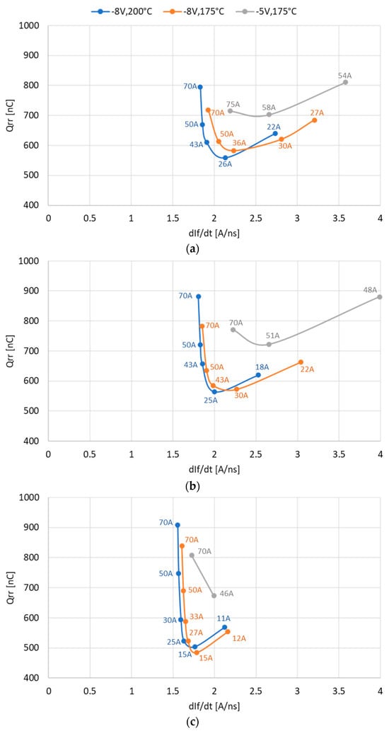
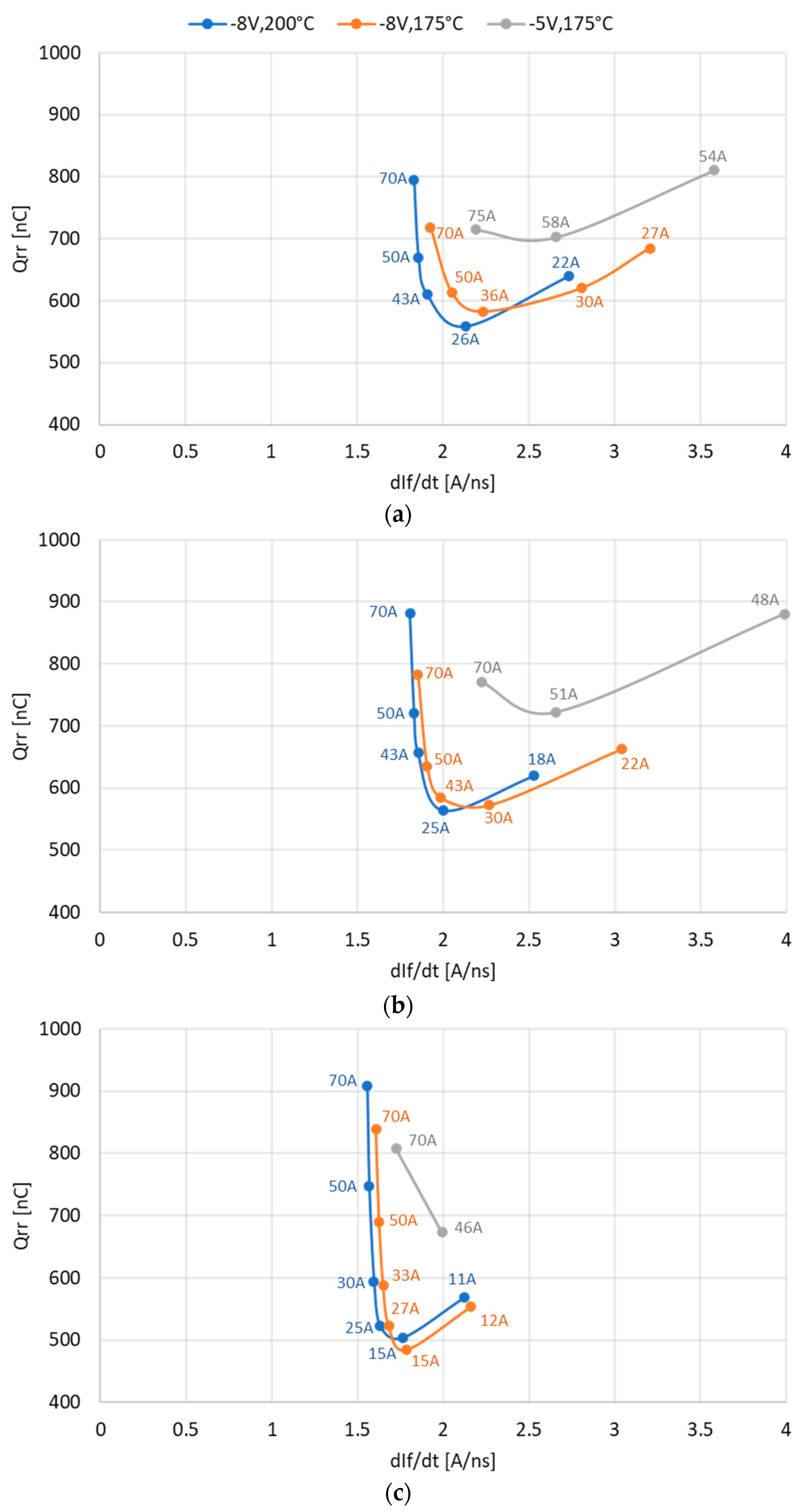
Figure 19.
Qrr evaluation at the snappy recovery limit condition as a function of dif/dt and If for three devices: (a) “Min”, (b) “Typ” and (c) “Max”.
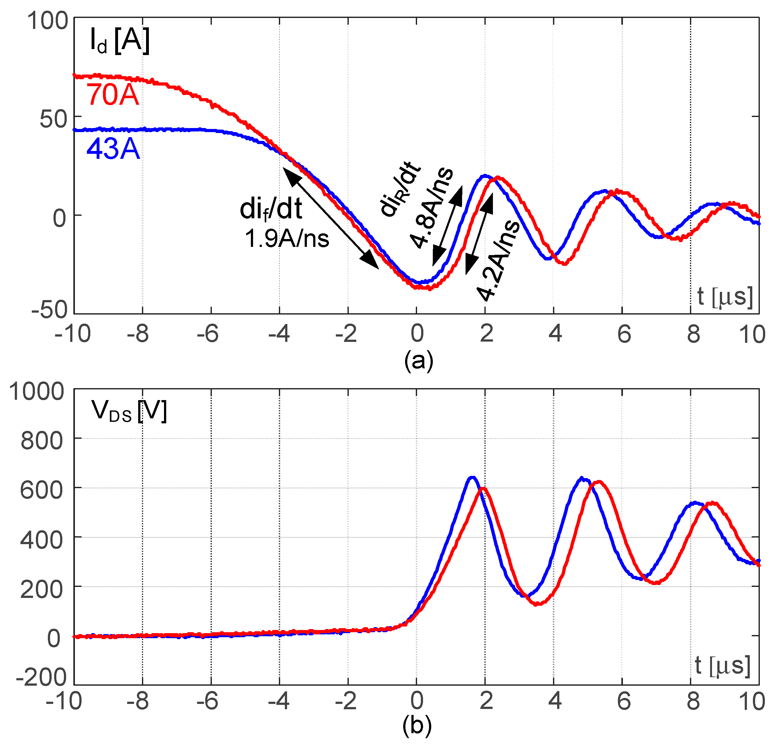
Figure 20 highlights the current and the Vds voltage of the typical device at VG_L = −8 V, Tj = 200 °C and two different conditions of forward current (43 A and 70 A), as already shown in Figure 19b. Both cases are snappy limit cases and, although they have different values of current, they have almost the same dif/dt. This analysis has highlighted the presence of a (dif/dt)min below which the recovery is not snappy, even for a high current level. Moreover, once (dif/dt)min is reached, Qrr depends only on If. It must be noted that this behavior is true in the case of VG_L = −8 V and Tc equal to 175 °C and 200 °C. In the case of VG_L = −5 V and Tc = 175 °C, the trend is quite different, since very high current and dif/dt are needed, so the condition of a (dif/dt)min is not reached. This limit is lower when the temperature (Figure 19) and the Vth (Figure 21) of the device are higher.
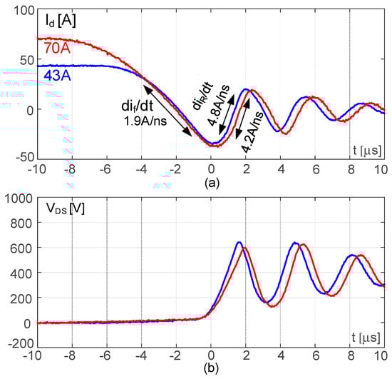
Figure 20.
(a) Forward current and (b) Vds voltage of device “Typ” at Tj = 200 °C, VG_L = −8 V and forward current of 43 A and 70 A.
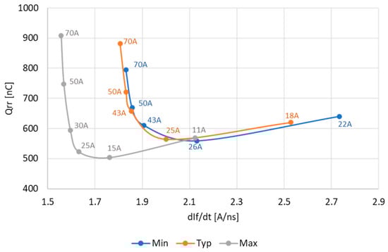
Figure 21.
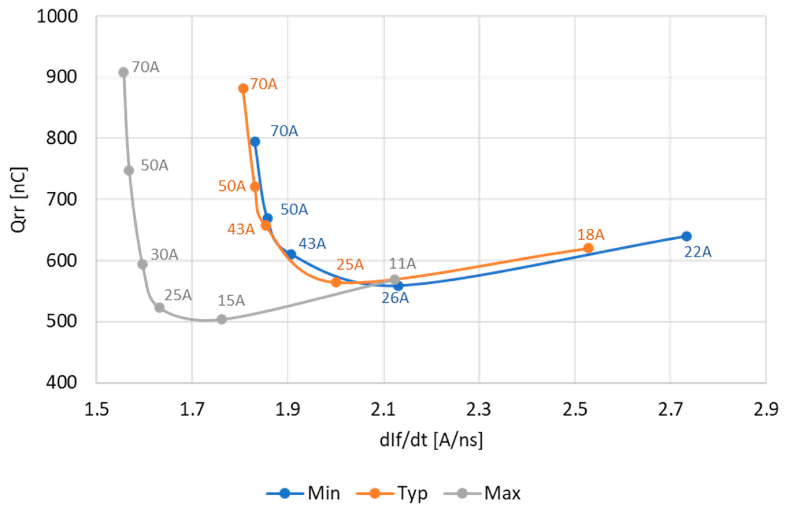
Qrr vs. dif/dt of three devices Min, Typ and Max at VG_L = −8 V and Tj = 200 °C.
This analysis allows us to understand the condition of a fast recovery at the operative condition boundary, and of the avoidance of the snappy recovery working region. According to the selected devices and their static parameters (in particular, the threshold voltage), snappy recovery can be triggered at a lower dif/dt and current when the Vth is higher. This aspect must be taken into account, especially in case of devices connected in parallel, as is usually the case in power modules.
In the analysis reported in Figure 19 and Figure 21, Qrr varies as a function of the forward current and dif/dt. There is a “valley” in the Qrr curves because Qrr decreases as the current decreases, while it increases as dif/dt increases, and the snappy condition occurs at high dif/dt and low current. More specifically, at low current, a further current reduction requires a very large increment in dif/dt to obtain snappy conditions, thus the effect of the latter is prevalent, showing an increment in Qrr, and consequently there is a “valley” in the curve. For example, in Figure 19a, at VG_L = −5 V/Tc = 175 °C (grey curve), to obtain the snappy condition passing from a current of 58 A to 54 A, it is necessary to increase the dif/dt by about 40%. Therefore, the reduction in the current (−6.9%) is smaller than the dif/dt increment, thus the overall effect is a Qrr increment, accounting for the “valley”.
5. Conclusions
The reverse recovery charge (Qrr) at different operating conditions and the limit conditions at which snappy recovery occurs have been analyzed in this paper. More specifically, the analysis of the reverse recovery charge, Qrr, revealed two unexpected phenomena at high temperatures: it decreases with increasing gate voltage; the higher the device threshold, the higher the Qrr. TCAD-Silvaco simulations have shown that this is due to a displacement current flowing in the drift region due to the output capacitance voltage variation during commutation. From the analysis of the snappy recovery, it emerged that there is a minimum forward current slope, below which the reverse recovery cannot be snappy, even for a high current level. Once this current slope is reached, Qrr varies with the forward current only.
This analysis is useful in defining a set of conditions in order to be able to force or avoid snappy recovery occurrence. Although these results are noteworthy, further investigations on this topic are necessary. One interesting research path in this field is the development of models that help us better understand and explain the phenomena in other devices. Another is to provide formula of the reverse recovery loss and snappy conditions. From this perspective, it is necessary to check the reverse recovery response for each SiC MOSFET, since it depends on many parameters, on the technology structure (planar, trench, etc.) and the generation (on the market there are now devices of different suppliers belonging to the third or fourth generation, and typically, from one generation to the next one, there are modifications in technical properties).
The results of this work suggest that it is important to check static parameters as well as evaluate Qrr trends and threshold limits of snappy recovery in real systems. This aspect is crucial in some applications, such as power modules for traction inverters where different SiC MOSFETs are connected in parallel, to ensure a balanced response during reverse recovery.
Author Contributions
Conceptualization, G.P., M.P., A.G.S., L.S. and S.A.R.; data curation, G.P., M.P., A.G.S., L.S. and S.C.; formal analysis, G.P., M.P. and N.S.; investigation, G.P. and M.P.; methodology, G.P., M.P., A.G.S., L.S. and A.L.; supervision, M.P. and S.A.R.; validation, M.P., A.G.S., L.S. and S.C.; visualization, G.P. and S.C.; writing—original draft, G.P., M.P. and N.S.; writing—review and editing, G.P., M.P., A.L. and S.A.R. All authors have read and agreed to the published version of the manuscript.
Funding
This research received no external funding.
Data Availability Statement
The original contributions presented in the study are included in the article, further inquiries can be directed to the corresponding author.
Conflicts of Interest
Giuseppe Pennisi, Mario Pulvirenti, Luciano Salvo, Angelo Giuseppe Sciacca and Salvatore Cascino were employed by the company ST Microelectronics Co., Ltd. Antonio Laudani, Nunzio Salerno and Santi Agatino Rizzo declare that the research was conducted in the absence of any commercial or financial relationships that could be construed as a potential conflict of interest.
References
- Eskandari, S.; Peng, K.; Tian, B.; Santi, E. Accurate Analytical Switching Loss Model for High Voltage SiC MOSFETs Includes Parasitics and Body Diode Reverse Recovery Effects. In Proceedings of the IEEE Energy Conversion Congress and Exposition, Portland, OR, USA, 23–27 September 2018; pp. 1867–1874. [Google Scholar]
- Rahimo, M.T. A comprehensive study of failure mode in IGBT applications due to freewheeling diode snappy recovery. In Proceedings of the Conference Record of 1998 IEEE Industry Applications Conference. Thirty-Third IAS Annual Meeting (Cat. No.98CH36242), St. Louis, MO, USA, 12–15 October 1998; Volume 2, pp. 840–847. [Google Scholar]
- Kumar, A.; Vechalapu, K.; Bhattacharya, S.; Veliadis, V.; Van Brunt, E.; Grider, D.; Sabri, S.; Hull, B. Effect of capacitive current on reverse recovery of body diode of 10 kV SiC MOSFETs and external 10 kV SiC JBS diodes. In Proceedings of the IEEE 5th Workshop on Wide Bandgap Power Devices and Applications (WiPDA), Albuquerque, NM, USA, 30 October–1 November 2017; pp. 208–212. [Google Scholar]
- Xue, P.; Maresca, L.; Riccio, M.; Breglio, G.; Irace, A. Self-sustained Oscillation of Superjunction MOSFET Intrinsic Diode During Reverse Recovery Transient. In Proceedings of the 31st International Symposium on Power Semiconductor Devices and ICs (ISPSD), Shanghai, China, 19–23 May 2019. [Google Scholar]
- Khorasani, A.E.; Griswold, M.; Alford, T.L. Gate-Controlled Reverse Recovery for Characterization of LDMOS Body Diode. IEEE Electron Device Lett. 2014, 35, 1079–1081. [Google Scholar] [CrossRef]
- Lindberg-Poulsen, K.; Petersen, L.P.; Ouyang, Z.; Andersen, M.A.E. Practical investigation of the gate bias effect on the reverse recovery behavior of the body diode in power MOSFETs. In Proceedings of the International Power Electronics Conference (IPEC-Hiroshima 2014—ECCE ASIA), Hiroshima, Japan, 18–21 May 2014. [Google Scholar]
- Choo, V.L.; Pfost, M.; Gessner, J.; Heinrich, K.; Eckoldt, U.; Liew, M.; Hao, Y. Reverse Recovery and Carrier Lifetime in Body Diodes of LDMOS Transistors. In Proceedings of the 2021 33rd International Symposium on Power Semiconductor Devices and ICs (ISPSD), Nagoya, Japan, 30 May–3 June 2021. [Google Scholar]
- Ferrara, A.; Siemieniec, R.; Medic, U.; Hutzler, M.; Blank, O.; Henson, T. Evolution of reverse recovery in trench MOSFETs. In Proceedings of the 2020 32nd International Symposium on Power Semiconductor Devices and ICs (ISPSD), Vienna, Austria, 13–18 September 2020. [Google Scholar]
- Xue, Z.; Zhu, M.; Cui, H.; Yang, F.; Pei, Y.; Wang, L. TCAD Modeling of Temperature-Dependent Reverse Recovery Characteristics of 1.2-kV SiC MOSFETs’ Body Diode. In Proceedings of the 2023 IEEE Energy Conversion Congress and Exposition (ECCE), Nashville, TN, USA, 29 October–2 November 2023. [Google Scholar]
- Li, P.; Ma, R.; Yang, Z.; Guo, J.; Lin, Z.; Hu, S. A Novel Approach to Suppress the Inhomogeneous Reverse Recovery Behavior of the Body Diode in Superjunction MOSFET. In Proceedings of the 2022 IEEE 16th International Conference on Solid-State & Integrated Circuit Technology (ICSICT), Nangjing, China, 25–28 October 2022. [Google Scholar]
- Qian, C.; Wang, Z.; Zhou, D.; Ge, Y.; Zhou, Y.; Xingyuan, Y.; Xin, G.; Shi, X. Investigation of Reverse Recovery Phenomenon for SiC MOSFETs in High-Temperature Applications. IEEE Trans. Power Electron. 2023, 38, 14375–14387. [Google Scholar] [CrossRef]
- An, J.; Hu, S. Heterojunction Diode Shielded SiC Split-Gate Trench MOSFET With Optimized Reverse Recovery Characteristic and Low Switching Loss. IEEE Access 2019, 7, 28592–28596. [Google Scholar] [CrossRef]
- Huang, M.; Li, R.; Yang, Z.; Ma, Y.; Li, Y.; Zhang, X.; Gong, M. A Multiepi Superjunction MOSFET With a Lightly Doped MOS-Channel Diode for Improving Reverse Recovery. IEEE Trans. Electron Devices 2021, 68, 2401–2407. [Google Scholar] [CrossRef]
- Liu, F.; Ruan, X. Analysis of the Body Diode Reverse Recovery of MOSFETs in ZVS PWM Combined Three-level Converter. In Proceedings of the 2007 IEEE Power Electronics Specialists Conference, Orlando, FL, USA, 17–21 June 2007. [Google Scholar]
- Bernal, C.; Jimenez, M. Adherence of a high-speed RRP LDMOS characterization setup to JESD 24-10 standard. In Proceedings of the IEEE 8th Latin American Symposium on Circuits & Systems (LASCAS), Bariloche, Argentina, 20–23 February 2017. [Google Scholar]
- Kanemoto, M.; Aoki, M.; Mochizuki, A.; Murakami, Y.; Tsunoda, M.; Yoshinari, G.; Nakano, N. Comparison of thermal stress under TCT between SiC and Si power devices using direct chip-bonding with ag sintered layer on Cu plate. In Proceedings of the 2017 IEEE Electrical Design of Advanced Packaging and Systems Symposium (EDAPS), Haining, China, 14–16 December 2017. [Google Scholar]
- Zhou, X.; Jia, Y.; Hu, D.; Wu, Y. A Simulation-Based Comparison Between Si and SiC MOSFETs on Single-Event Burnout Susceptibility. IEEE Trans. Electron Devices 2019, 66, 2551–2556. [Google Scholar] [CrossRef]
- Chen, J.; Deng, E.; Zhao, Z.; Wu, Y.; Huang, Y. Power Cycling Capability Comparison of Si and SiC MOSFETs under Different Conduction Modes. In Proceedings of the 2020 32nd International Symposium on Power Semiconductor Devices and ICs (ISPSD), Vienna, Austria, 13–18 September 2020. [Google Scholar]
- Naik, H.; Chow, P.T. Comparison of AC I-V characteristic of Si and SiC MOSFETs. In Proceedings of the 2012 Lester Eastman Conference on High Performance Devices (LEC), Providence, RI, USA, 7–9 August 2012. [Google Scholar]
- Qi, F.; Fu, L.; Xu, L.; Jing, P.; Zhao, G.; Wang, J. Si and SiC power MOSFET characterization and comparison. In Proceedings of the 2014 IEEE Conference and Expo Transportation Electrification Asia-Pacific (ITEC Asia-Pacific), Beijing, China, 31 August–3 September 2014. [Google Scholar]
- Bouchetob, E.; Nadji, B.; Mahdi, I. Efficiency comparison of silicon and silicon carbide MOSFETs in a PV system application. In Proceedings of the 2023 International Conference on Advances in Electronics, Control and Communication Systems (ICAECCS), BLIDA, Algeria, 6–7 March 2023. [Google Scholar]
- Sachdev, N.; Bhat, A.K.S. Performance comparison of Si and SiC MOSFETs in a bidirectional dual half-bridge series resonant converter. In Proceedings of the 2018 International Conference on Power, Instrumentation, Control and Computing (PICC), Thrissur, India, 18–20 January 2018. [Google Scholar]
- Kibushi, R.; Hatakeyama, T.; Yuki, K.; Unno, N.; Ishizuka, M. Comparison of thermal properties between Si and SiC power MOSFET using electro-thermal analysis. In Proceedings of the 2017 International Conference on Electronics Packaging (ICEP), Yamagata, Japan, 19–22 April 2017. [Google Scholar]
- Bhat, A.; Bhatt, N. Design and Performance Comparison of Si and SiC MOSFETs for Dual Tank LCL-Type Series Resonant Converter. In Proceedings of the 2019 IEEE Conference on Energy Conversion (CENCON), Yogyakarta, Indonesia, 16–17 October 2019. [Google Scholar]
- Blinov, A.; Chub, A.; Vinnikov, D.; Rang, T. Feasibility study of Si and SiC MOSFETs in high-gain DC/DC converter for renewable energy applications. In Proceedings of the IECON 2013—39th Annual Conference of the IEEE Industrial Electronics Society, Vienna, Austria, 10–13 November 2013. [Google Scholar]
- Jordan, J.; Esteve, V.; Sanchis-Kilders, E.; Dede, E.J.; Maset, E.; Ejea, J.B.; Ferreres, A. A Comparative Performance Study of a 1200 V Si and SiC MOSFET Intrinsic Diode on an Induction Heating Inverter. IEEE Trans. Power Electron. 2014, 29, 2550–2562. [Google Scholar] [CrossRef]
- Gui, H.; Zhang, Z.; Ren, R.; Chen, R.; Niu, J.; Tolbert, L.M.; Wang, F.; Blalock, B.J.; Cositinett, D.J.; Choi, B.B. SiC MOSFET Versus Si Super Junction MOSFET-Switching Loss Comparison in Different Switching Cell Configurations. In Proceedings of the 2018 IEEE Energy Conversion Congress and Exposition (ECCE), Portland, OR, USA, 23–27 September 2018. [Google Scholar]
- Kibushi, R.; Hatakeyama, T.; Yuki, K.; Unno, N.; Ishizuka, M. Comparison of hot spot temperature between Si and SiC power MOSFET using electro-thermal analysis. In Proceedings of the 2017 16th IEEE Intersociety Conference on Thermal and Thermomechanical Phenomena in Electronic Systems (ITherm), Orlando, FL, USA, 30 May–2 June 2017. [Google Scholar]
- Chen, Z.; Boroyevich, D.; Li, J. Behavioral comparison of Si and SiC power MOSFETs for high-frequency applications. In Proceedings of the 2013 Twenty-Eighth Annual IEEE Applied Power Electronics Conference and Exposition (APEC), Long Beach, CA, USA, 17–21 March 2013. [Google Scholar]
- Pulvirenti, M.; Sciacca, A.G.; Salvo, L.; Nania, M.; Scelba, G.; Scarcella, G. Body Diode Reverse Recovery Effects on SiC MOSFET Half-Bridge Converters. In Proceedings of the IEEE Energy Conversion Congress and Exposion (ECCE), Detroit, MI, USA, 11–15 October 2020; pp. 2871–2877. [Google Scholar]
- Nayak, D.P.; Yakala, R.K.; Kumar, M.; Pramanick, S.K. Temperature-Dependent Reverse Recovery Characterization of SiC MOSFETs Body Diode for Switching Loss Estimation in a Half-Bridge. IEEE Trans. Power Electron. 2022, 37, 5574–5582. [Google Scholar] [CrossRef]
- Liu, X.; Li, X.; Hermann, C.; Blaser, T. The Impact of the Dead-Time on the Reverse Recovery Behavior of SiC-MOSFET Body Diodes. In Proceedings of the International Symposium on Power Semiconductor Devices and ICs (ISPSD), Hong Kong, China, 28 May–1 June 2023. [Google Scholar]
- Kumar, A.; Bhattacharya, S.; Baliga, J. Influence of the Inverter Dead-time on the Reverse Recovery Characteristics of 3.3-kV SiC MOSFETs and JBSFETs. In Proceedings of the IEEE Energy Conversion Congress and Exposition (ECCE), Detroit, MI, USA, 9–13 October 2022. [Google Scholar]
- Qi, J.; Tian, K.; Mao, Z.; Yang, S.; Song, W.; Zhang, A. Dynamic Characterization of 1.2 kV SiC Power MOSFET Body Diode at Cryogenic and High Temperatures. In Proceedings of the 1st Workshop on Wide Bandgap Power Devices and Applications in Asia (WiPDA Asia), Xi’an, China, 16–18 May 2018. [Google Scholar]
- Hou, X.; Boroyevich, D.; Burgos, R. Characterization on latest-generation SiC MOSFET’s body diode. In Proceedings of the 4th Workshop on Wide Bandgap Power Devices and Applications (WiPDA), Fayetteville, AR, USA, 7–9 November 2016. [Google Scholar]
- Zhang, D.; Horii, K.; Hata, K.; Takamiya, M. Digital Gate Driver IC with Real-Time Gate Current Change by Sensing Drain Current to Cope with Operating Condition Variations of SiC MOSFET. In Proceedings of the 2023 11th International Conference on Power Electronics and ECCE Asia (ICPE 2023—ECCE Asia), Jeju Island, Republic of Korea, 22–25 May 2023. [Google Scholar]
- Roy, S.K.; Basu, K. An Energy based Approach to Calculate Actual Switching Loss for SiC MOSFET from Experimental Measurement. In Proceedings of the 2021 IEEE 12th International Symposium on Power Electronics for Distributed Generation Systems (PEDG), Chicago, IL, USA, 28 June–1 July 2021. [Google Scholar]
- Ahmed, M.R.; Todd, R.; Forsyth, A.J. Switching performance of a SiC MOSFET body diode and SiC schottky diodes at different temperatures. In Proceedings of the 2017 IEEE Energy Conversion Congress and Exposition (ECCE), Cincinnati, OH, USA, 1–5 October 2017. [Google Scholar]
- Cameron, A.; Hopkins, A.; Simpson, N.; Mellor, P. Low Temperature Loss-Analysis of SiC MOSFETs for Integrated Motor Drive Applications. In Proceedings of the 2023 IEEE Energy Conversion Congress and Exposition (ECCE), Nashville, TN, USA, 29 October–2 November 2023. [Google Scholar]
- Sarnowska, A.; Rabkowski, J. Hard and soft switching operation of the half-bridge based on 900V SiC MOSFETs. In Proceedings of the IECON 2016—42nd Annual Conference of the IEEE Industrial Electronics Society, Florence, Italy, 23–26 October 2016. [Google Scholar]
- Chen, X.; Jiang, S.; Chen, Y.; Gou, H.; Xie, Q.; Shen, B. Transient Modeling and Loss Analysis of SiC MOSFETs at Cryogenic and Room Temperatures. IEEE Trans. Appl. Supercond. 2021, 31, 1400404. [Google Scholar] [CrossRef]
- Song, Q.; Wang, W.; Zhang, S.; Li, Y.; Ahmad, M. The analysis of power losses of power inverter based on SiC MOSFETs. In Proceedings of the 2019 1st Global Power, Energy and Communication Conference (GPECOM), Nevsehir, Turkey, 12–15 June 2019. [Google Scholar]
- Rashid, A.U.; Brooks, B.; Manz, S.; Lichtenwalner, D.J.; Ryu, S.-H. Modeling of the Snappy, and Soft Reverse Recovery of SiC MOSFET’s Body Diode. In Proceedings of the IEEE BiCMOS and Compound Semiconductor Integrated Circuits and Technology Symposium (BCICTS), Monterey, CA, USA, 16–18 October 2023. [Google Scholar]
- Di Luca Cardillo, G.; Salvo, L.; Pulvirenti, M.; Sciacca, A.G.; Cascino, S.; Rizzo, S.A.; Scelba, G.; Salerno, N. Investigation of the limit conditions of SiC MOSFET body diode reverse recovery. In Proceedings of the IEEE Energy Conversion Congress and Exposition (ECCE), Nashville, TN, USA, 29 October–2 November 2023. [Google Scholar]
- Marz, A.; Schonewolf, S.; Nagel, A.; Rauh, M.; Bakran, M.-M. Deadtime optimization eliminating snap-off of 3.3kV SiC MOSFET bodydiodes. In Proceedings of the 2023 25th European Conference on Power Electronics and Applications (EPE’23 ECCE Europe), Aalborg, Denmark, 4–8 September 2023. [Google Scholar]
- Li, X.; Xiao, F.; Luo, Y.; Wang, R.; Duan, Y. Modeling of High-Voltage Nonpunch-Through PIN Diode Snappy Reverse Recovery and Its Optimal Suppression Method Based on RC Snubber Circuit. IEEE Trans. Ind. Electron. 2022, 69, 5700–5712. [Google Scholar] [CrossRef]
- Karout, M.A.; Taha, M.; Fisher, C.A.; Deb, A.; Mawby, P.; Alatise, O. Impact of Diode Characteristics on 1.2 kV SiC MOSFET and Cascode JFET Efficiency: Body Diodes Vs SiC Schottky Barrier Diodes. In Proceedings of the 2023 IEEE Applied Power Electronics Conference and Exposition (APEC), Orlando, FL, USA, 19–23 March 2023. [Google Scholar]
- Awwad, A.E.; Dieckerhoff, S. Operation of planar and trench SiC MOSFETs in a 10kW DC/DC-converter analyzing the impact of the body diode. In Proceedings of the 2017 IEEE Energy Conversion Congress and Exposition (ECCE), Cincinnati, OH, USA, 1–5 October 2017. [Google Scholar]
- Ahmed, M.R.; Todd, R.; Forsyth, A.J. Predicting SiC MOSFET Behavior Under Hard-Switching, Soft-Switching, and False Turn-On Conditions. IEEE Trans. Ind. Electron. 2017, 64, 9001–9011. [Google Scholar] [CrossRef]


Disclaimer/Publisher’s Note: The statements, opinions and data contained in all publications are solely those of the individual author(s) and contributor(s) and not of MDPI and/or the editor(s). MDPI and/or the editor(s) disclaim responsibility for any injury to people or property resulting from any ideas, methods, instructions or products referred to in the content. |
© 2024 by the authors. Licensee MDPI, Basel, Switzerland. This article is an open access article distributed under the terms and conditions of the Creative Commons Attribution (CC BY) license (https://creativecommons.org/licenses/by/4.0/).