
A Family of 5-Level Boost-Active Neutral-Point-Clamped (5L-BANPC) Inverters with Full DC-Link Voltage Utilization Designed Using Half-Bridges

Abstract
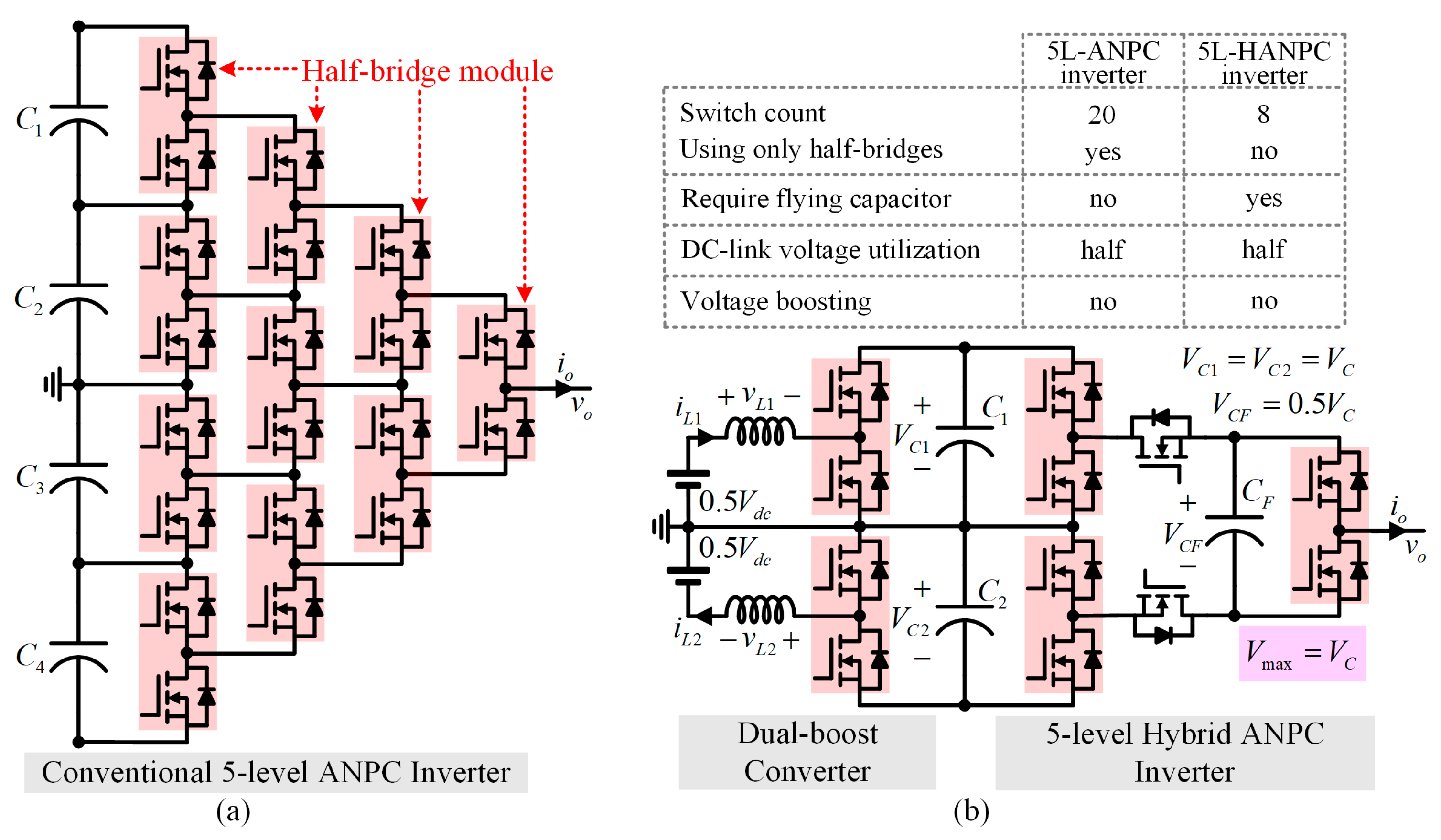
:1. Introduction
- (1)
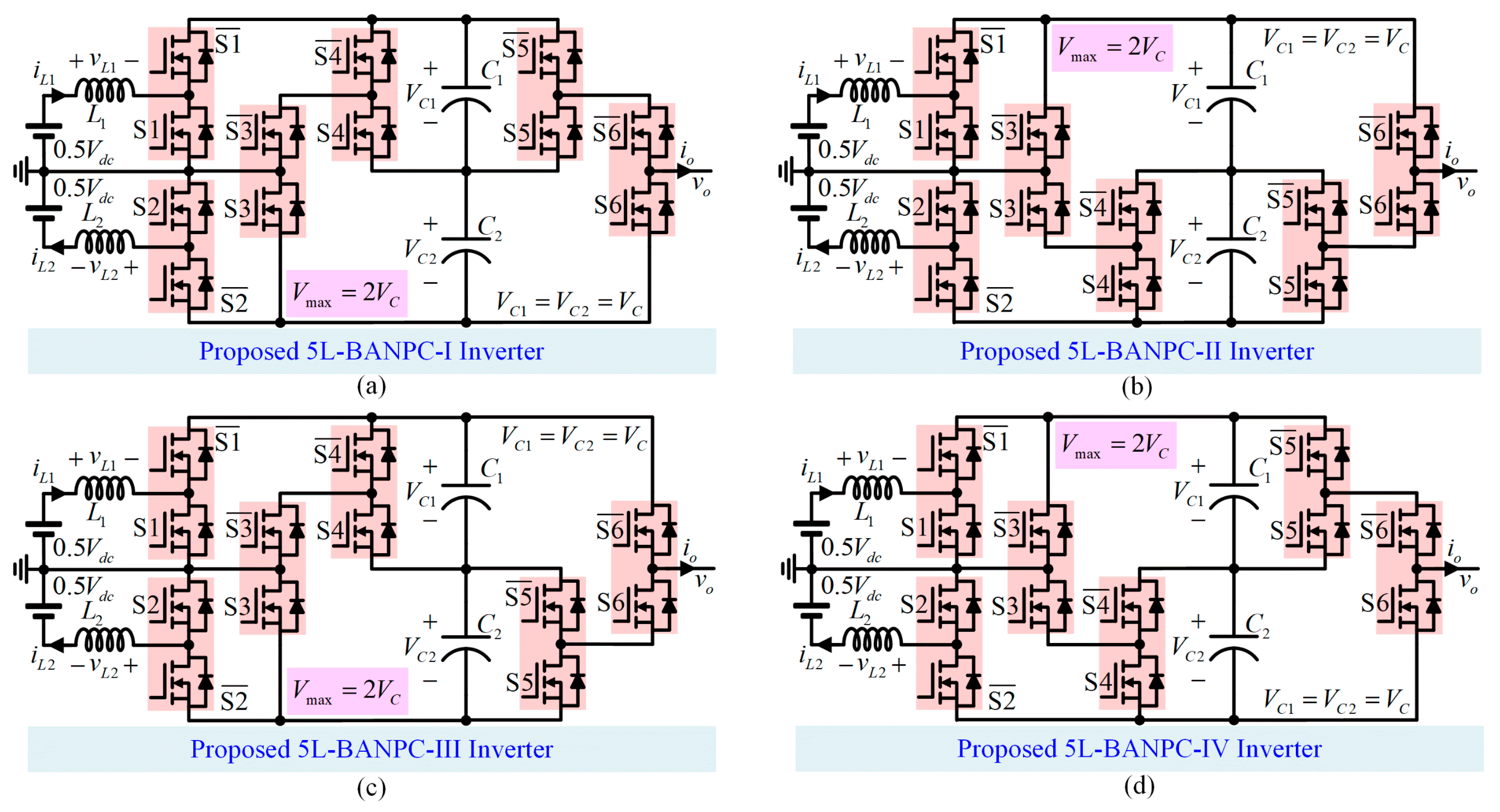
- Only two dc-link capacitors are sufficient for generating five voltage levels without requiring any flying capacitors.
- (2)
- The voltage across dc-link capacitors is naturally balanced without requiring any controllers or sensors.
- (3)
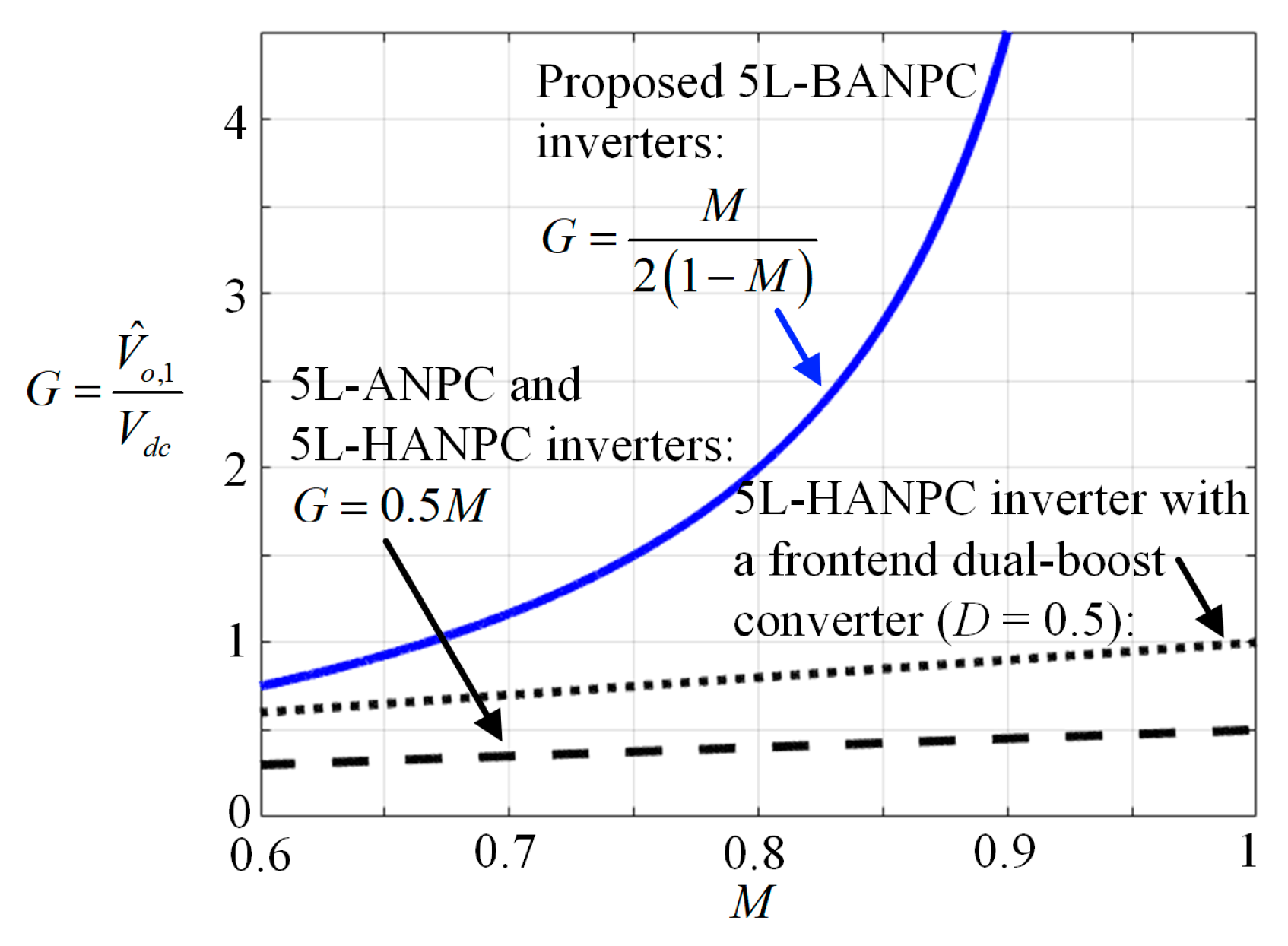
- Full dc-link voltage utilization with the maximum voltage level is generated by the entire dc-link voltage 2VC which is double that of the existing 5L-ANPC and 5L-HANPC topologies.
- (4)
- The proposed topologies achieved dynamic voltage boosting using only 12 switches. They can be easily implemented using six commercial half-bridge cells/modules without requiring a dedicated power circuit design.
- (5)
- All benefits are achieved without using the concept of an SC circuit; therefore, they resolve the issues associated with the existing SC-based ANPC inverters, such as current spikes.
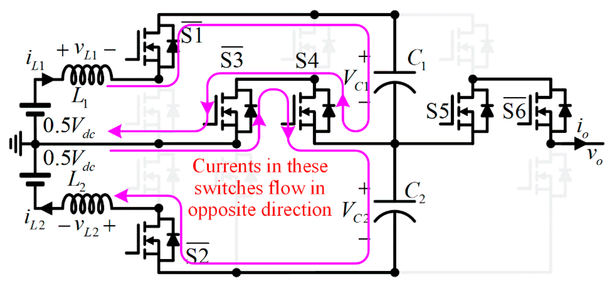
2. Proposed 5-Level Boost ANPC Inverters
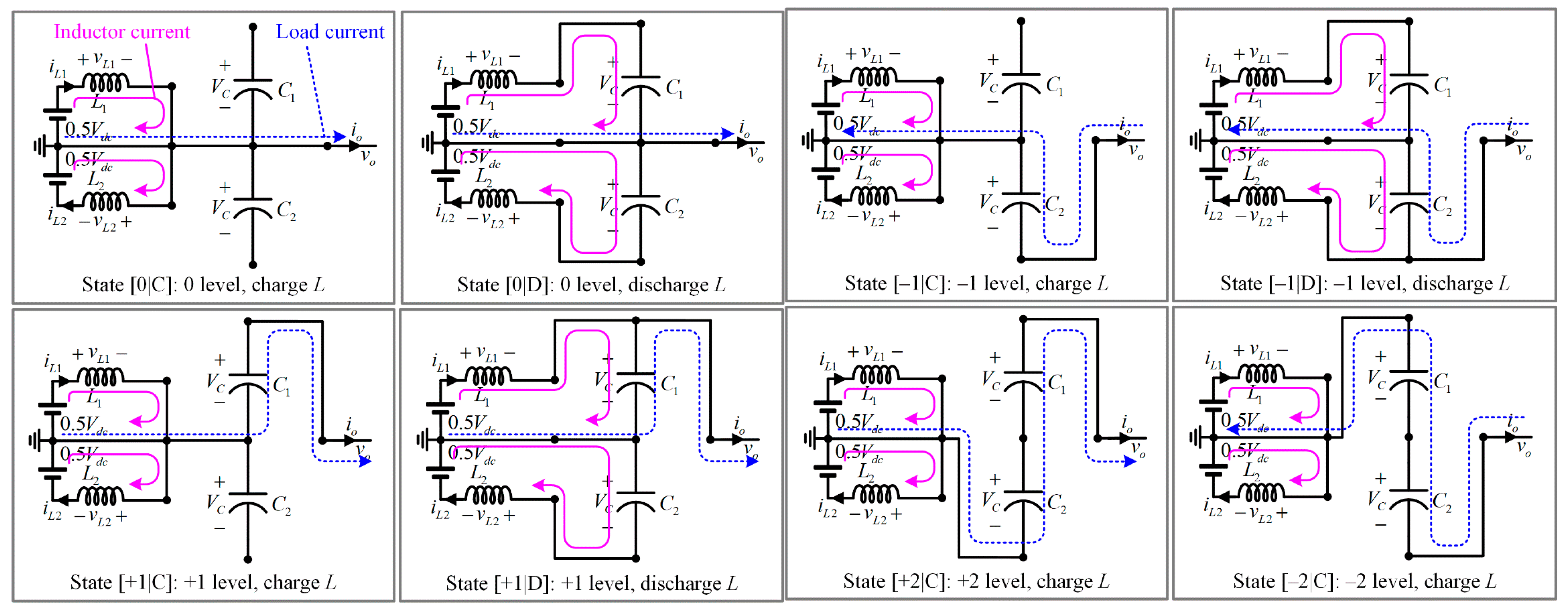
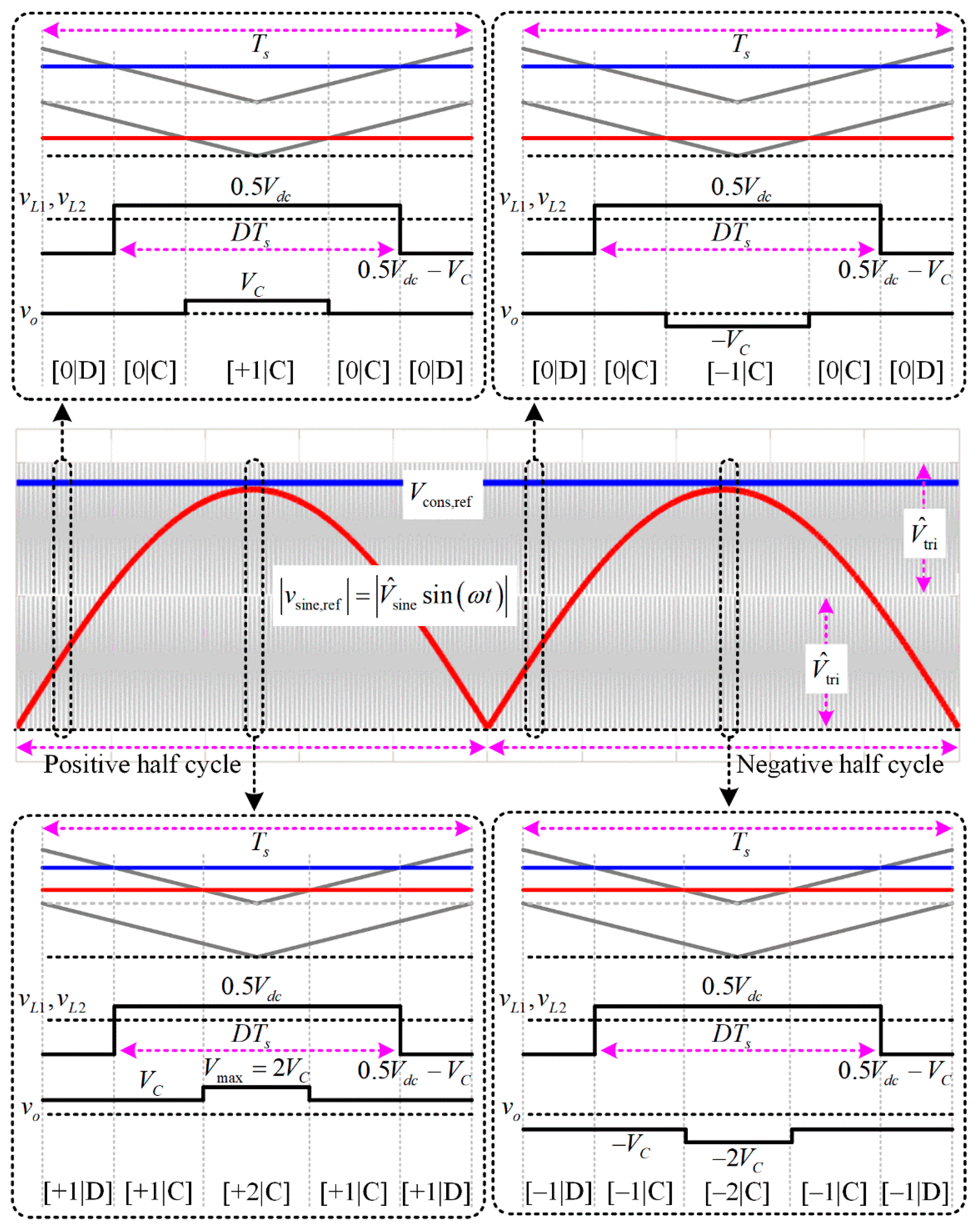
2.1. Operating Principle
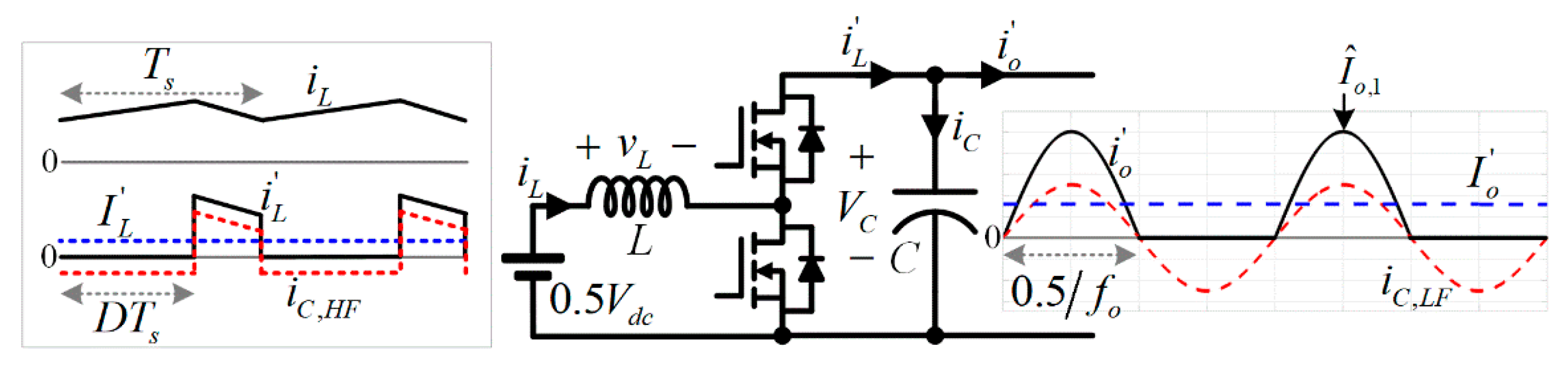
2.2. Ripple Analysis
2.3. Current Stress Analysis
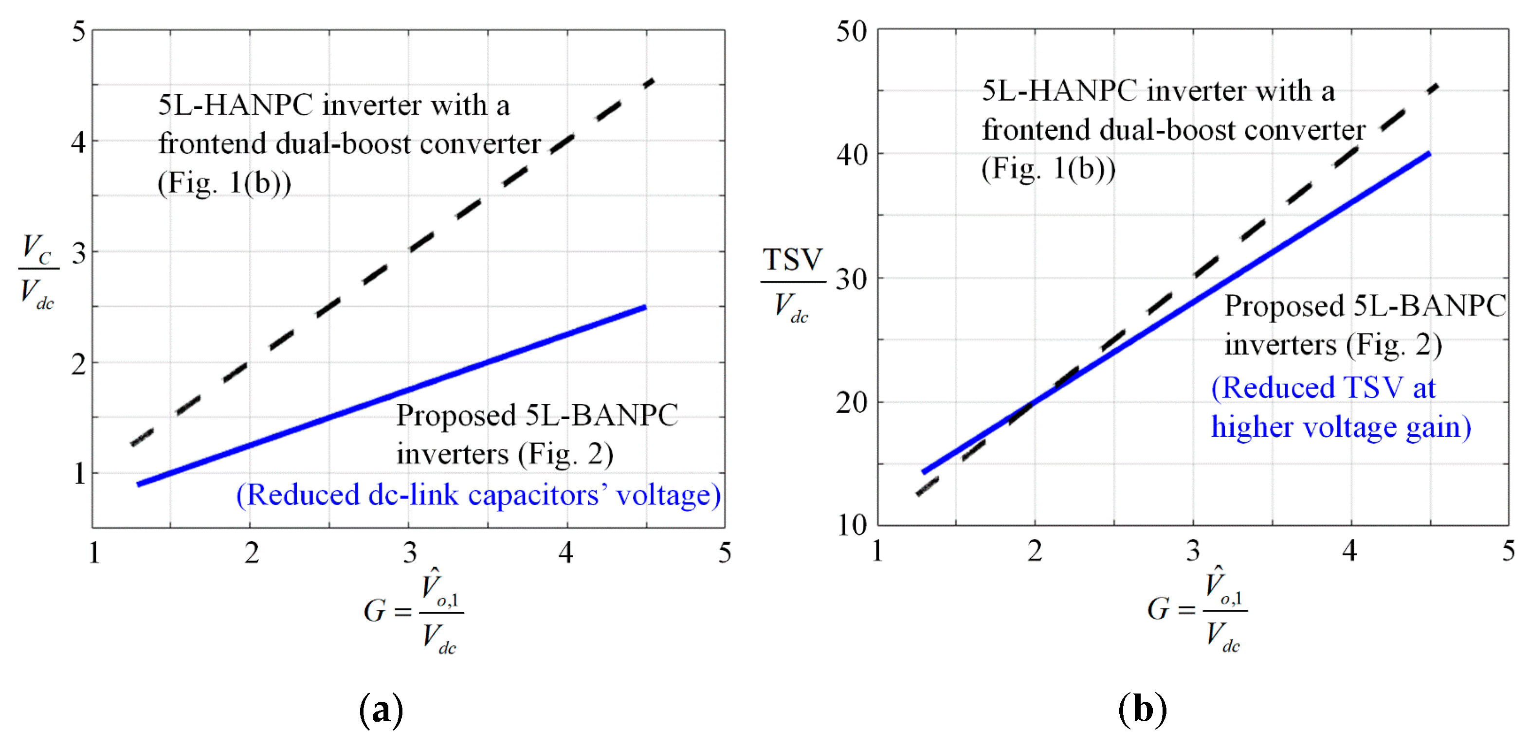
2.4. Voltage Stress Analysis
2.5. Comparison with the Latest 5-Level ANPC Topologies
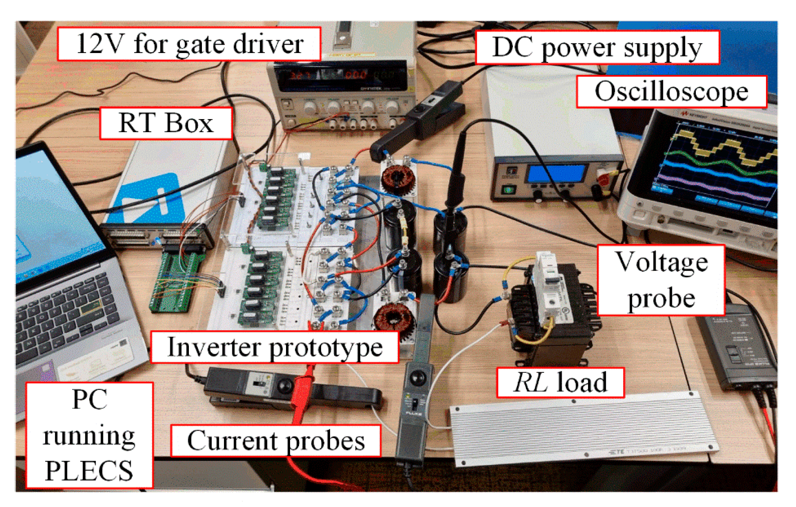
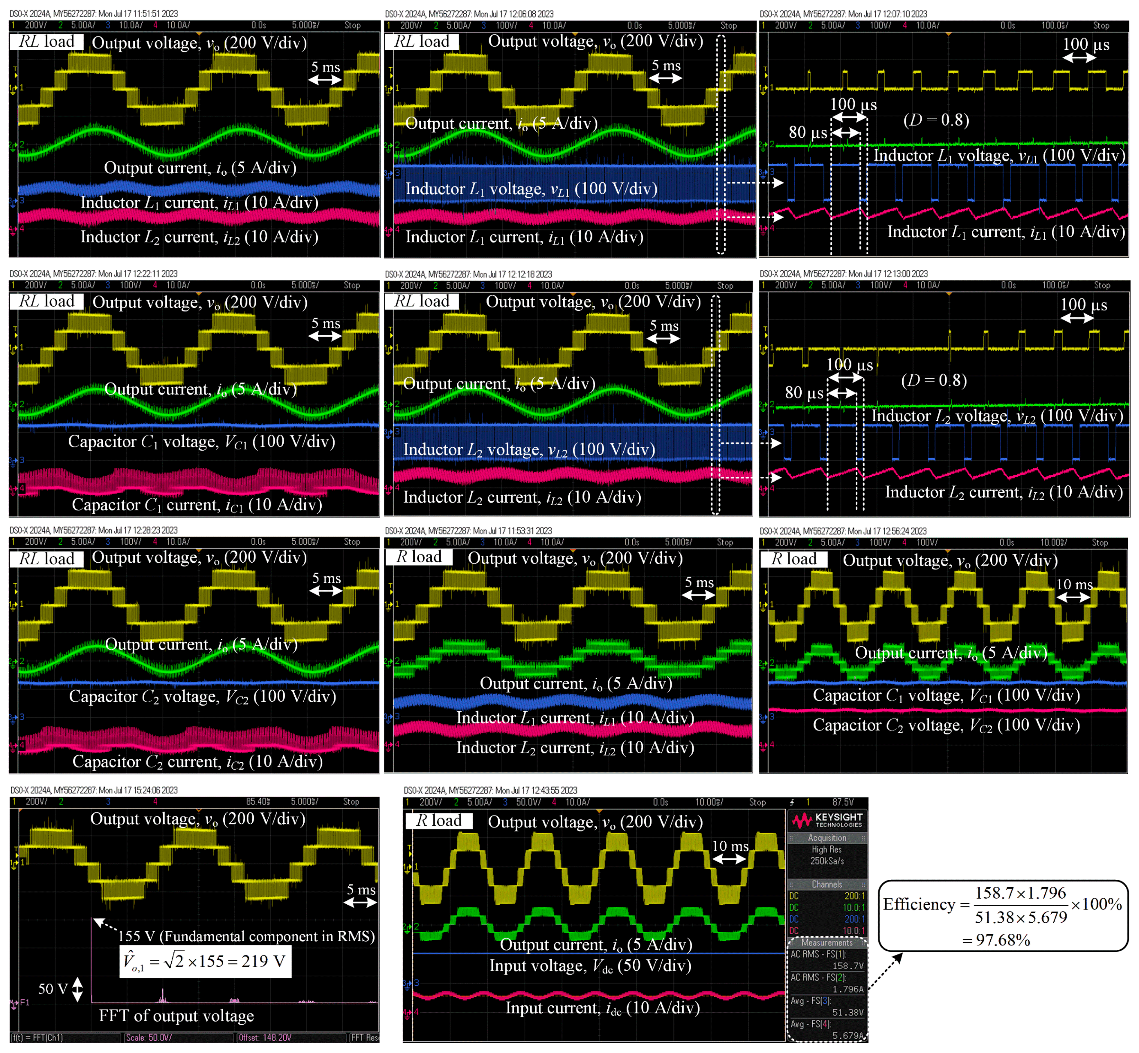
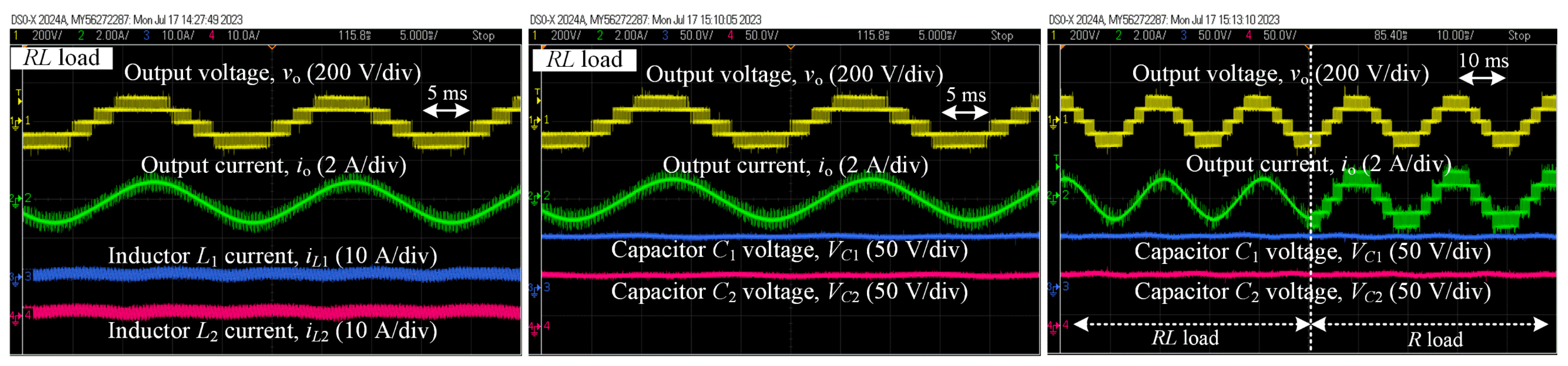
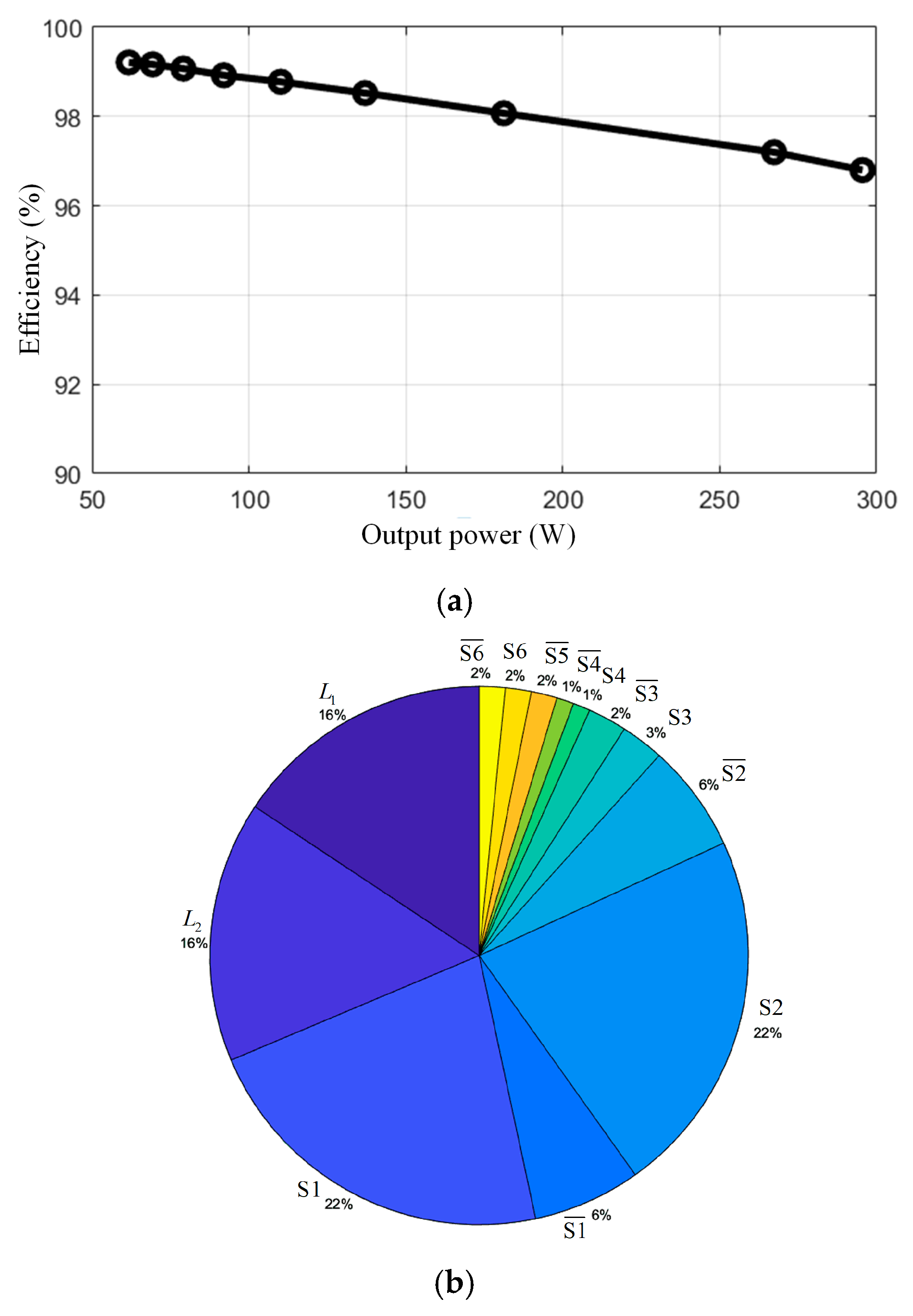
3. Results
4. Conclusions
Funding
Data Availability Statement
Acknowledgments
Conflicts of Interest
References
- Nabae, A.; Takahashi, I.; Akagi, H. A New Neutral-Point-Clamped PWM Inverter. IEEE Trans. Ind. Appl. 1981, IA-17, 518–523. [Google Scholar] [CrossRef]
- Akagi, H. Multilevel Converters: Fundamental Circuits and Systems. Proc. IEEE 2017, 105, 2048–2065. [Google Scholar] [CrossRef]
- Li, Y.; Li, Y.W. The Evolutions of Multilevel Converter Topology: A Roadmap of Topological Invention. IEEE Ind. Electron. Mag. 2021, 16, 11–18. [Google Scholar] [CrossRef]
- Kouro, S.; Leon, J.I.; Vinnikov, D.; Franquelo, L.G. Grid-Connected Photovoltaic Systems: An Overview of Recent Research and Emerging PV Converter Technology. IEEE Ind. Electron. Mag. 2015, 9, 47–61. [Google Scholar] [CrossRef]
- Leon, J.I.; Vazquez, S.; Franquelo, L.G. Multilevel Converters: Control and Modulation Techniques for Their Operation and Industrial Applications. Proc. IEEE 2017, 105, 2066–2081. [Google Scholar] [CrossRef]
- Bruckner, T.; Bemet, S. Loss balancing in three-level voltage source inverters applying active NPC switches. In Proceedings of the 2001 IEEE 32nd Annual Power Electronics Specialists Conference (IEEE Cat. No. 01CH37230), Vancouver, BC, Canada, 17–21 June 2001; pp. 1135–1140. [Google Scholar]
- Li, Y.; Tian, H.; Li, Y.R. Matrix-Based Approach for Open-Circuit Fault-Tolerant Analysis and PWM Design of Active Neutral-Point-Clamped Converters. IEEE Trans. Power Electron. 2022, 37, 14706–14719. [Google Scholar] [CrossRef]
- Wodajo, E.T.; Wodajo, E.T.; Elbuluk, M.E.; Elbuluk, M.E.; Choi, S.; Choi, S.; Abu-Rub, H.; Abu-Rub, H. Three Parts Modulation and Hybrid DC Capacitor Voltage Balancing for a Single-Phase Two-Leg Five-Level NPC Inverter. IEEE Trans. Ind. Electron. 2022, 70, 6765–6775. [Google Scholar] [CrossRef]
- Barbosa, P.; Steimer, P.; Meysenc, L.; Winkelnkemper, M.; Steinke, J.; Celanovic, N. Active neutral-point-clamped multilevel converters. In Proceedings of the 2005 IEEE 36th Power Electronics Specialists Conference, Dresden, Germany, 16 June 2005; pp. 2296–2301. [Google Scholar]
- Wang, H.; Kou, L.; Liu, Y.-F.; Sen, P.C. A Seven-Switch Five-Level Active-Neutral-Point-Clamped Converter and Its Optimal Modulation Strategy. IEEE Trans. Power Electron. 2016, 32, 5146–5161. [Google Scholar] [CrossRef]
- Wang, H.; Kou, L.; Liu, Y.-F.; Sen, P.C. A New Six-Switch Five-Level Active Neutral Point Clamped Inverter for PV Applications. IEEE Trans. Power Electron. 2016, 32, 6700–6715. [Google Scholar] [CrossRef]
- Alsofyani, I.M.M.; Lee, K.-B. Simple Capacitor Voltage Balancing for Three-Level NPC Inverter Using Discontinuous PWM Method With Hysteresis Neutral-Point Error Band. IEEE Trans. Power Electron. 2021, 36, 12490–12503. [Google Scholar] [CrossRef]
- Cui, D.; Ge, Q. A Novel Hybrid Voltage Balance Method for Five-Level Diode-Clamped Converters. IEEE Trans. Ind. Electron. 2018, 65, 6020–6031. [Google Scholar] [CrossRef]
- Siwakoti, Y.P.; Palanisamy, A.; Mahajan, A.; Liese, S.; Long, T.; Blaabjerg, F. Analysis and Design of a Novel Six-Switch Five-Level Active Boost Neutral Point Clamped Inverter. IEEE Trans. Ind. Electron. 2020, 67, 10485–10496. [Google Scholar] [CrossRef]
- Ye, Y.; Hua, T.; Chen, S.; Wang, X. Neutral-Point-Clamped Five-Level Inverter with Self-Balanced Switched Capacitor. IEEE Trans. Ind. Electron. 2021, 69, 2202–2215. [Google Scholar] [CrossRef]
- Zhang, W.; Wang, H.; Zhu, X.; Wang, H.; Deng, X.; Yue, X. A Three-Phase Five-Level Inverter with High DC Voltage Utilization and Self-Balancing Capacity of Floating Capacitor. IEEE Trans. Power Electron. 2022, 37, 10609–10619. [Google Scholar] [CrossRef]
- Lee, S.S.; Lee, K.-B. Dual-T-Type Seven-Level Boost Active-Neutral-Point-Clamped Inverter. IEEE Trans. Power Electron. 2019, 34, 6031–6035. [Google Scholar] [CrossRef]
- Pal, P.K.; Jana, K.C.; Siwakoti, Y.P.; Majumdar, S.; Blaabjerg, F. An Active-Neutral-Point-Clamped Switched-Capacitor Multilevel Inverter With Quasi-Resonant Capacitor Charging. IEEE Trans. Power Electron. 2022, 37, 14888–14901. [Google Scholar] [CrossRef]
- Lee, S.S.; Lim, C.S.; Lee, K.-B. Novel Active-Neutral-Point-Clamped Inverters with Improved Voltage-Boosting Capability. IEEE Trans. Power Electron. 2019, 35, 5978–5986. [Google Scholar] [CrossRef]
- Barzegarkhoo, R.; Forouzesh, M.; Lee, S.S.; Blaabjerg, F.; Siwakoti, Y.P. Switched-Capacitor Multilevel Inverters: A Comprehensive Review. IEEE Trans. Power Electron. 2022, 37, 11209–11243. [Google Scholar] [CrossRef]
- Rech, C.; Castiblanco, W.A.P. Five-Level Switched-Capacitor ANPC Inverter with Output Voltage Boosting Capability. IEEE Trans. Ind. Electron. 2022, 70, 29–38. [Google Scholar] [CrossRef]
- Lee, S.S.; Siwakoti, Y.P.; Barzegarkhoo, R.; Lee, K.-B. Five-Level Unity-Gain Active Neutral-Point-Clamped Inverters Designed Using Half-Bridges. IEEE Trans. Ind. Appl. 2023, 59, 3520–3529. [Google Scholar] [CrossRef]


| Switching State | Operation of Half-Bridges: S1 S2 S3 S4 S5 S6 | |||
|---|---|---|---|---|
| 5L-BANPC-I Inverter | 5L-BANPC-II Inverter | 5L-BANPC-III Inverter | 5L-BANPC-IV Inverter | |
| [0|C] | 110110 | 111001 | 110101 | 111010 |
| [0|D] | 000110 | 001001 | 000101 | 001010 |
| [+1|C] | 110100 | 111000 | 110100 | 111000 |
| [+1|D] | 000100 | 001000 | 000100 | 001000 |
| [−1|C] | 110111 | 111011 | 110111 | 111011 |
| [−1|D] | 000111 | 001011 | 000111 | 001011 |
| [+2|C] | 111100 | 111100 | 111100 | 111100 |
| [−2|C] | 110011 | 110011 | 110011 | 110011 |
| Switch | Voltage Stress | |||
|---|---|---|---|---|
| 5L-BANPC-I Inverter | 5L-BANPC-II Inverter | 5L-BANPC-III Inverter | 5L-BANPC-IV Inverter | |
| VC | VC | VC | VC | |
| 2VC | 2VC | 2VC | 2VC | |
| VC | VC | VC | VC | |
| 2VC | 2VC | 2VC | 2VC | |
| 2VC | VC | 2VC | VC | |
| VC | 2VC | VC | 2VC | |
| VC | VC | VC | VC | |
| VC | VC | VC | VC | |
| VC | VC | VC | VC | |
| VC | VC | VC | VC | |
| 2VC | VC | VC | 2VC | |
| VC | 2VC | 2VC | VC | |
| Topology | (a) | (b) | (c) | (d) | (e) | (f) | (g) | (h) |
|---|---|---|---|---|---|---|---|---|
| [15] | No | 5 | 2 | 4 | 1 | No | 0.5M | No |
| [16] | No | 10 | 2 | 3 | 1 | Yes | M | No |
| [21] | No | 8 | 0 | 3 | 0 | Yes | M | No |
| [22] | Yes | 8 | 2 | 3 | 0 | Yes | M | No |
| Figure 1b | No | 12 | 0 | 3 | 2 | No | Yes | |
| Proposed 5L-BANPC | Yes | 12 | 0 | 2 | 2 | Yes | Yes |
| Parameter | Value |
|---|---|
| Input voltage, Vdc | 50 V |
| Output power | 300 W |
| Inductor: L1, L2 | 500 µH |
| Capacitor: C1, C2 | 1000 μF |
| Carrier frequency | 10 kHz |
| Load resistor | 100 Ω |
| Load inductor | 100 mH |
| Output frequency | 50 Hz |
| Component/Equipment | Part Number |
|---|---|
| DC Supply | EA-PS 5200-10 A |
| Inductor: L1, L2 | NAC-13-0501 |
| Capacitor: C1, C2 | LNY2W102MSEF |
| Power MOSFET | C2M0080120D |
| Digital oscilloscope | DSO-X 2024A |
| Differential voltage probe | Fluke DP120 |
| Current probe | Fluke 80i-110s |
Disclaimer/Publisher’s Note: The statements, opinions and data contained in all publications are solely those of the individual author(s) and contributor(s) and not of MDPI and/or the editor(s). MDPI and/or the editor(s) disclaim responsibility for any injury to people or property resulting from any ideas, methods, instructions or products referred to in the content. |
© 2024 by the author. Licensee MDPI, Basel, Switzerland. This article is an open access article distributed under the terms and conditions of the Creative Commons Attribution (CC BY) license (https://creativecommons.org/licenses/by/4.0/).
Share and Cite
Lee, S.S. A Family of 5-Level Boost-Active Neutral-Point-Clamped (5L-BANPC) Inverters with Full DC-Link Voltage Utilization Designed Using Half-Bridges. Energies 2024, 17, 2798. https://doi.org/10.3390/en17122798
Lee SS. A Family of 5-Level Boost-Active Neutral-Point-Clamped (5L-BANPC) Inverters with Full DC-Link Voltage Utilization Designed Using Half-Bridges. Energies. 2024; 17(12):2798. https://doi.org/10.3390/en17122798
Chicago/Turabian StyleLee, Sze Sing. 2024. "A Family of 5-Level Boost-Active Neutral-Point-Clamped (5L-BANPC) Inverters with Full DC-Link Voltage Utilization Designed Using Half-Bridges" Energies 17, no. 12: 2798. https://doi.org/10.3390/en17122798