Review

Non-Linear Phenomena in Voltage and Frequency Converters Supplying Non-Thermal Plasma Reactors

by
Grzegorz Karol Komarzyniec
,
Henryka Danuta Stryczewska
* and
Oleksandr Boiko
Department of Electrical Engineering and Superconductivity Technologies, Lublin University of Technology, 38A Nadbystrzycka Street, 20-618 Lublin, Poland
*
Author to whom correspondence should be addressed.
Energies 2024, 17(12), 2846; https://doi.org/10.3390/en17122846
Submission received: 29 March 2024 / Revised: 3 June 2024 / Accepted: 6 June 2024 / Published: 9 June 2024
(This article belongs to the Special Issue Energy, Electrical and Power Engineering 2024)

Abstract

:
Atmospheric pressure cold plasmas have recently been the subject of intense research and applications for solving problems in the fields of energy, environmental engineering, and biomedicine. Non-thermal atmospheric pressure plasma sources, with dielectric barrier discharges, plasma jets, and arc discharges, are non-linear power loads. They require special power systems, which are usually designed separately for each type of plasma reactor, depending on the requirements of the plasma-chemical process, the power of the receiver, the type of process gas, the current, voltage and frequency requirements, and the efficiency of the power source. This paper presents non-linear phenomena accompanying plasma generation in the power supply plasma reactor system, such as harmonic generation, resonance, and ferroresonance of currents and voltages, and the switching of overvoltages and pulse generation. When properly applied, this can support the operation of the above-mentioned reactors by providing improved discharge ignition depending on the working gas, thus increasing the efficiency of the plasma process and improving the cooperation of the plasma-generation system with the power supply.

1. Introduction

Atmospheric pressure cold plasma (APCP), produced by electrical discharge, is finding increasing application in such interdisciplinary scientific and technological fields as energy, environment, agriculture, and medicine. However, plasma technology is constantly being developed. Its energy efficiency cannot be directly compared with mature thermal and chemical conversion technologies.
Plasma technology facilities are more compact, have shorter response times and are relatively inexpensive compared to conventional solutions such as CO2 conversion, energy storage, and non-CO2 natural gas reforming. These processes use only air, water, and renewable energy sources as feedstock and have all the advantages of plasma technology as an environmentally friendly solution. A target efficiency of 60% has been proposed in the literature to make plasma CO2 conversion competitive with existing processes, and some types of plasma reactors, such as gliding arc discharge (GAD) plasma reactors, are very promising in this respect [1,2].
The aim of this review is to prove that phenomena unfavourable for the power supplies of non-linear plasma receivers, such as the generation of higher current and voltage harmonics, resonance and ferroresonance phenomena, and the switching of overvoltages and energy pulses, which we usually deal with in voltage and frequency converters, can be used to improve the operating parameters of the power supply plasma reactor system on the basis of selected examples, including from our own research and those of other authors dealing with the issue of power supplies for plasma reactors.
Reactors for the production of APCP are non-linear electrical energy receivers that use various types of electrical discharge and, depending on the application, have different power outputs, from several hundred watts (in medical and agricultural applications) to as much as several dozen kilowatts (for energy and environmental engineering applications).
Such plasma reactors (PRs) can be supplied with DC—pulsed and sinusoidal voltages at frequencies ranging from a few hertz—through radio frequency (RF) in the order of several kilohertz or even hundreds of megahertz (microwave reactors). The power supplies of such plasma reactors include voltage converters (high-voltage transformers, magnetic switches, and chokes) and frequency converters (thyristor and transistor inverters, pulse generators and magnetic frequency converters). Such power supply systems (PSS) can be classified as static voltage and/or frequency converters (VFC). They must meet the specific requirements of atmospheric pressure cold plasma (APCP) reactors, which include the following: (1) The type of discharge used to generate the plasma; (2) The composition and physical and chemical parameters of the gas; (3) The pressure in the discharge chamber; (4) The geometrical parameters of the discharge elements (volume of the discharge plenum, type of dielectric or lack thereof; (5) The need to ensure ignition of the discharge and to maintain cyclic operation of the PR after ignition; (6) The power, voltage, frequency, number of phases and impedance of the power supply system; elements improving the interaction of the power supply with the mains, like frequency filters and reactive power compensators.
Recently, pulsed power supplies (PPS) have been increasingly used to supply energy to the PR. PPS enable stable discharge conditions at high pressure and low temperature and very often do not require a cooling system, which relatively simplifies the construction of the plasma reactor. Pulsed power (PP) is delivered to the discharge chamber only during the ionisation and recombination processes when active particles are produced, which in the air are responsible for initiating electron reactions of dissociation with oxygen, nitrogen, ions, and UV radiation. These active particles, such as atomic oxygen O, superoxide anion O2, ozone O3, singlet oxygen 1O2, nitric oxide NO, dinitrogen oxide N2O, nitrite ion N O 2 nitrate ion N O 3 , and many others, are used in plasma-chemical processes for sterilisation, disinfection, removal of sulphur dioxide (SO2) from flue gases and volatile organic substances (VOCs) emitted in industrial painting processes, and the decomposition of carbon dioxide (CO2) [3].
In PSS, the discharge power, which is a measure of the efficiency of the PR, is regulated by the voltage, current, and frequency value, depending on the type of electric discharge. The overview of APCP sources presented in this paper includes reactors with dielectric barrier discharges (DBDs), which are present in classic dielectric barrier (DB) discharge reactors as well as in atmospheric pressure plasma jets (APPJs) and with two- and multi-electrode gliding arc discharges (GADs), which can also be used as two-electrode APPJs.
The factors for this choice are the following: these types of electrical discharge produce APCPs; the design of the reactors is relatively simple; and the potential area of application is large, ranging from energy conversion processes and environmental clean-up to materials science, bioengineering, agriculture and medicine [4,5,6,7,8,9].

2. Plasma Reactors as Electrical Energy Receivers

The PSS discussed in this article are used to power plasma reactors (PRs) with DBDs, APPJs and GADs. Recently, they have been the most widely used in practical applications. APCP sources, depending on the type of discharge used to generate plasma, represent different loads for PSS.
In the following subsections, APCP reactors with DBDs, GADs, and APPJs are presented as energy loads. It is pointed out that these loads, depending on the presence or absence of a dielectric barrier in the reactor design, require an energy source with the characteristics of a real voltage source or a real current source, respectively. In addition, due to the non-linearity of the PR-PSS system, the phenomena of higher harmonic generation, resonance and ferroresonance of currents (IFR) and voltages (UFR), switching overvoltage (SO) and pulsed power generation (PP) may occur. These phenomena are usually considered detrimental to the performance of the PR-PSS and its interaction with the mains, but when properly exploited, as described in Section 4, they can improve the performance of APCP generation systems, as well as their interaction with the mains, which is particularly important in industrial systems.

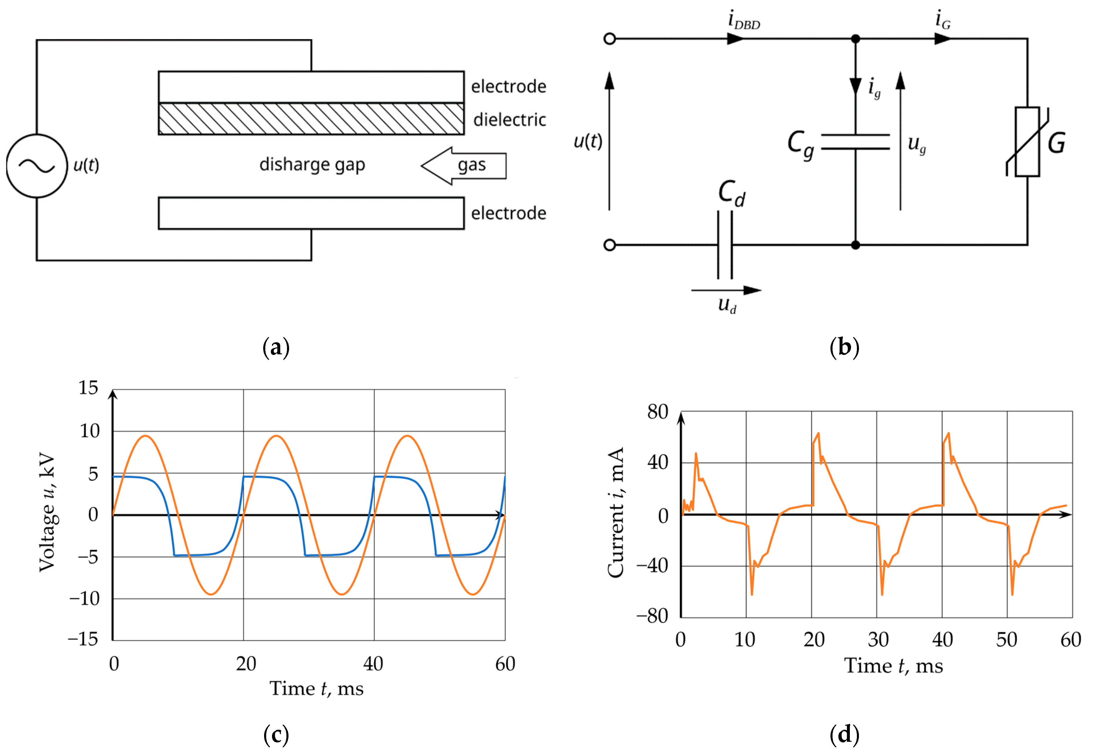
2.1. Plasma Reactor with DBD

The DBD reactor, for the power system, is a capacitive-resistive receiver with variable capacitance and non-linear post-ignition conductance of the discharge. When the voltage reaches the discharge ignition value, gas ionisation occurs, and the discharge gap loses its insulating properties. Figure 1 schematically shows the structure of the DBD PR (a) and its equivalent diagram (b).
DBD reactors do not require an additional discharge ignition system. The power of discharges and the energy efficiency of plasma generation in the DBD PRs depend on the following:
-
Geometric parameters of the discharge elements (shape, dimensions and surface Quality of electrodes, type and thickness of dielectric);
-
Physical and chemical parameters of the input gas (type and composition of gas, presence of impurities, temperature, humidity);
-
Electrical parameters of the power supply system (voltage value, frequency and shape, internal impedance).
The process of ozone and active particle formation during DBD is divided into three main stages. The first stage involves very fast ionisation and dissociation processes, lasting no longer than the time of a single current pulse, i.e., dozens of nanoseconds. The next stage, called recombination, in which active molecules are formed, is much slower and lasts a few microseconds. If, at this stage, all the oxygen atoms (in DBD in oxygen) were used to form ozone, the efficiency of the process would be maximised. As research has shown [10,11], this is only possible in the case of very weak micro-discharges. During stronger discharges, additional reactions begin to occur. As a result, oxygen atoms combine into bimolecular oxygen and react with the newly produced ozone, thus reducing the efficiency of the synthesis. The last stage of the cycle in question is diffusion, during which ozone molecules leave the gap. This stage lasts a few milliseconds and determines the duration of the entire synthesis cycle. The next pulse (voltage) of energy should appear only after this stage is completed; otherwise, the ozone particles formed during the recombination process will be destroyed, and the efficiency of the process will significantly decrease. Therefore, the supply voltage ensuring the ozone synthesis process with close to maximum efficiency should have the shape of a dozen-nanosecond voltage pulse with a frequency ranging from 50 Hz to several thousand Hz. A higher frequency also means more homogeneity of discharge (called glow) without sparking or arcing.
The efficiency of DBD discharges, which is measured by the active power P of a single discharge element, shown by Equation (1), depends on the voltage and frequency, as well as on the geometrical parameters of the discharge element of PR, the relative electrical permeability of the dielectric barrier (DB) and the type of gas for discharge.
P = 4 f C d U i g U m C g C r U i g C r = C g C d C g + C d ,
where f—frequency of PS, Cd—capacity of the DB, Cg—capacity of the discharge gap, Um—voltage magnitude, Uig—ignition voltage, Cr—the resultant capacity of the series-connected Cd and Cg.
The performance of the DBD reactor, as can be seen from Equation (1), can be improved by increasing the frequency of the supply voltage, but the increase in gas temperature in the discharge gap, which usually worsens the synthesis of particles and radicals in plasma processes and necessitates the use of special electrode cooling systems, must be taken into account. In industrial practice, frequencies of 150, 600 and 750 Hz are used. Higher supply voltage frequencies require both cooling of electrodes and the use of media other than water to cool the discharge elements.
The PSS for PR with discharges in the presence of DB have the characteristics of a voltage source, often at high frequencies, which makes it possible to reduce the supply voltage at which discharges occur and ensure their uniformity [12,13,14,15,16].

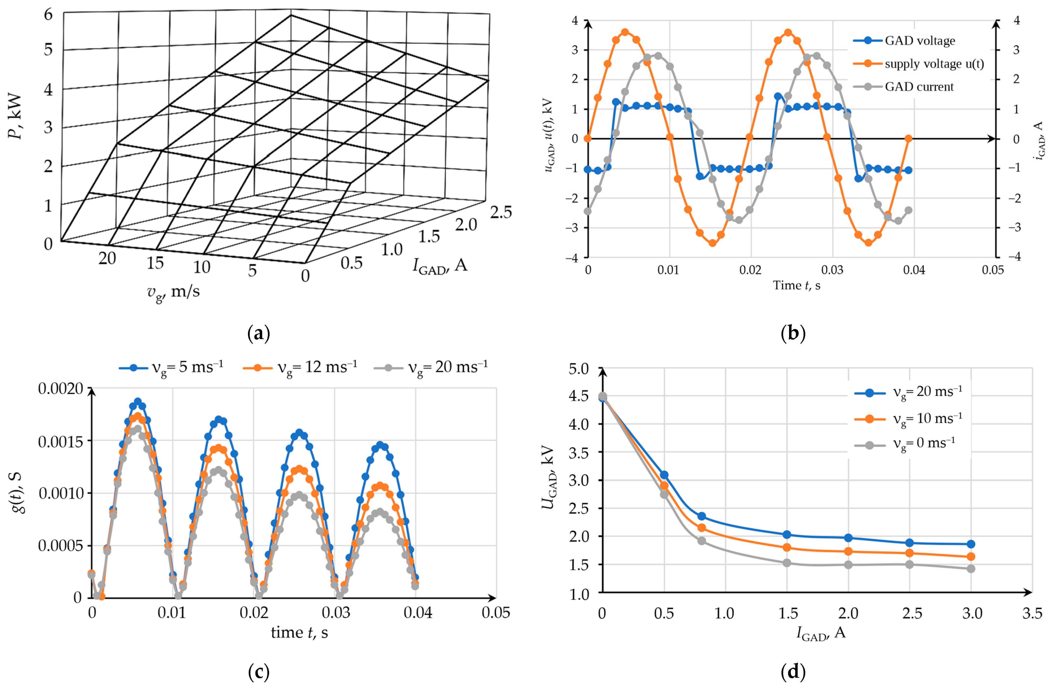
2.2. GAD Plasma Reactor

The GAD PR is a special APCP source. The discharge begins in the ignition area located above the process gas distribution nozzle. First, with the mains frequency power supply, a spark discharge appears, followed by an arc column whose volume and length increase gradually due to the fast gas flow and electrodynamic forces. By limiting the arc column current and its cyclic gliding movement, the thermodynamic imbalance increases and the discharge becomes a glow type. There is a significant imbalance between electron temperature and average gas temperature, due to which a source of high-energy electrons used in plasma-chemical processes is obtained. Maintaining this temperature regime from the perspective of the plasma process itself is beneficial due to both the thermal safety of materials subjected to plasma treatment using the GAD PR and the low energy consumption of the process [8,17,18,19].
The main feature of the gliding arc (GA) is its ability to generate APCP directly in the polluted gas under the conditions in which the exhaust gases are emitted into the atmosphere without the need for pretreatment. A GAD PR electrode sketch, its equivalent circuit, the theoretical voltage and current courses of the two-electrode GAD PR, and photos of GAD developing during the operating cycle from ignition to extinction under natural movement without forced gas flow are depicted in Figure 2 [19].
The characteristics of GAD PRs vary from those presented by reactors with other types of electrical discharge. The conductance of the interelectrode space, which depends on the degree of gas ionisation, changes significantly during each PR operation cycle and is greatest before ignition when the gas is not ionised. After ignition, it decreases rapidly and then increases again with a developing arc until the discharge at the point of the largest electrode distance is extinguished. The static and dynamic characteristics of a plasma reactor depend on many factors, the most important of which are PR geometry, type of working gas, and PSS parameters. By changing these factors, it is possible to influence the electrical and thermal parameters of the GA in the PR discharge chamber. By controlling the discharge power, plasma temperature, degree of ionisation of the working gas and its chemical composition and velocity, the parameters of the plasma-chemical process can be selected to achieve high efficiency and effectiveness.
A GAD PR for PSS is the non-linear resistive energy receiver that, depending on the composition of the working gas, requires an additional ignition system. After ignition, it is necessary to limit the reactor’s current in a fast and effective way in order to maintain the non-thermal conditions of the discharge. The GAD, as a receiver of electrical energy, and the PSS create a resistive-inductive circuit with non-linear and non-stationary parameters. With a sinusoidal supply voltage, the discharge current igad is practically sinusoidal, but the voltage of the discharge column ugad undergoes significant deformation (Figure 2) [19,20].
The duration of one PR operation cycle, from the ignition of the GA to its extinction at the ends of the electrodes, depends on their dimensions and shape, gas flow velocity, type and temperature and may vary from a few to a dozen periods of supply voltage at 50 Hz mains frequency. The movement of the GA and the extension and cooling of its column reduce its stability and may consequently lead to the quenching of the discharge. Small, random disturbances cause large changes in the shape of the GA, and determining the shape of the discharge path, its length and its speed, either theoretically or experimentally, is practically impossible.
The length of the GA during the single work cycle increases several times, and it depends on the electrode geometry, gas flow velocity, and usually non-linear internal reactance Xint of the PSS. The simplified relationship for the length of the GA during a single GAD PR work cycle, taking into account a constant gas flow at speed vg, the electrode angle β, is expressed as follows:
l G A t l 0 + β v g t ,
where l0—electrode spacing at the point of GA ignition at t0, β—electrode angle and vg—gas velocity (Figure 2a).
The dynamic current-voltage characteristic of the GA, given for the first time by the British engineer, mathematician, physicist and inventor Hertha Ayrton for an arc burning between carbon electrodes in air (in the 1902-published book The Electric Arc) and modified by the authors can be expressed by the following equation:
u G A D t = [ U 0 + E 0   l G A ( t ) ] s i g n i G A D ( t ) + P 0 + Q 0   l G A ( t ) i G A D ( t ) ,
where U0 + E0l0—interelectrode voltage for electrode distance equal to l0, in a place where the GA ignites, in V; E0—electric field intensity in the GA column, in V/m; P0—active power at the moment of GA ignition, in W; Q0—linear density of power received from the GA column as a result of heat conduction, in W/m; l G A t —GA length as a function of time, in m; s i g n i G A D ( t ) —sign of the GAD current, taking into account that the GA ignites and extinguishes in each half of the sinusoidal PR supply voltage (Figure 2a,b).
Representing the two-electrode PR with a GAD powered by a real voltage source with a single-phase equivalent circuit shown in Figure 2b, when powered by a sinusoidal voltage and taking into account Equation (3) and assuming that the internal reactance of the Xint power supply is linear, the circuit equation from Figure 2b will take the form of the following:
U m s i n ω t + φ u = X i n t ω d i G A D t d t + U 0 + E 0   l G A t s i g n i G A D t + P 0 + Q 0   l G A t i G A D t .
Equation (4) is a first-order non-linear differential one, and its analytical solution without additional simplifying assumptions is impossible due to the non-linearity of the voltage–current characteristic of GAD u G A D ( t ) = f i G A D ( t ) and the singularities occurring in solution. The calculations of Equation (4) were performed for the parameters of the reactor model presented in Table 1, and selected analysis results are shown in Figure 3.
As can be seen from both the instantaneous current and voltage waveforms and the static GAD characteristics (Figure 3), PSS for PR with GAD should represent a real current source. The GAD current is practically sine, and after the GA’s ignition voltage is constant, it is between 1.5 and 1.6 kV in the case of air as a processing gas (see Figure 3d). Therefore, regulation of active power P is practically possible by changing the RMS value of the current to a much greater extent than the value of the PSS voltage.

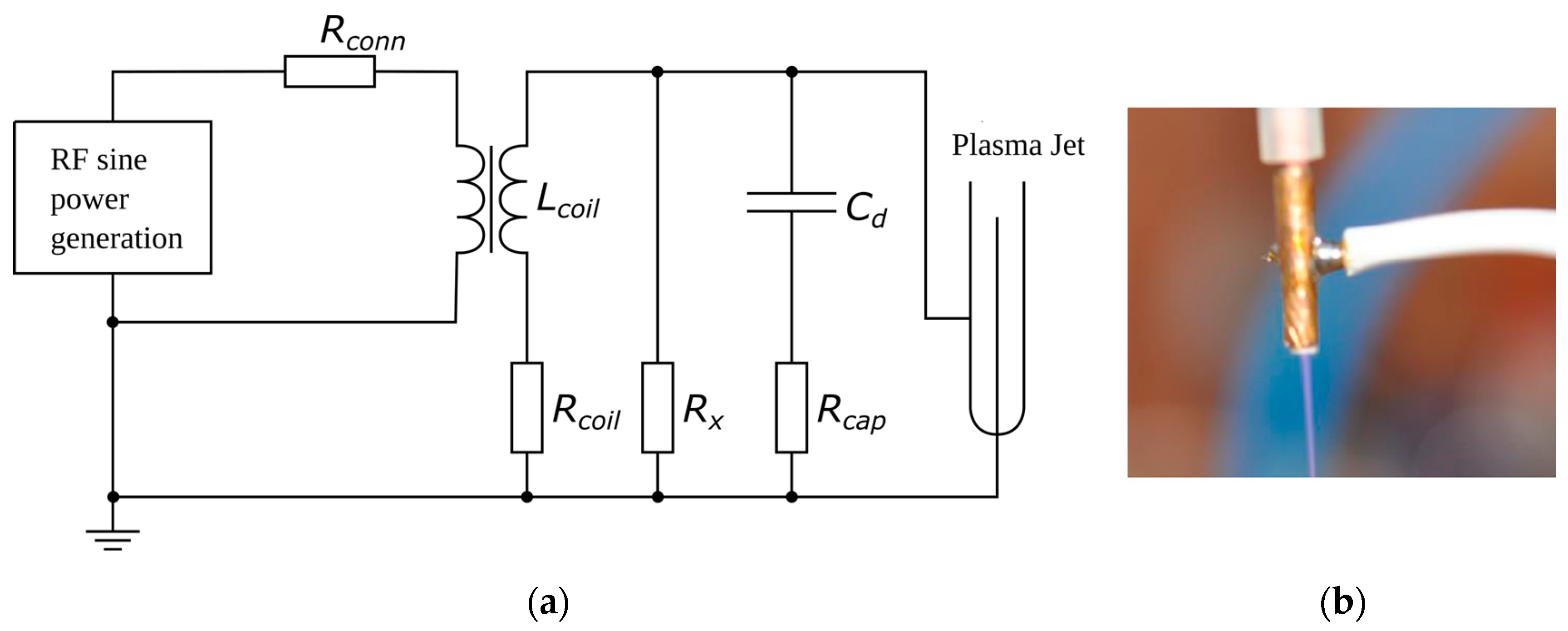
2.3. Atmospheric Pressure Plasma Jets

APPJ-type reactors are used to generate stable low-temperature plasma, which allows for directional impact on objects of various shapes and dimensions. They are also used in biological decontamination and medical applications, as well as for surface treatment and modification. APPJs are usually equipped with a nozzle where the plasma is generated. The forced gas flow transports the generated plasma outside the reactor toward the object undergoing plasma-chemical treatment, taking the shape of a uniform after-glow discharge.
Currently, several different approaches are available in APPJ technology to achieve non-equilibrium plasma conditions at atmospheric pressure. These include gas flow conditions, electric field geometry and, first of all, appropriate selection of the electricity supply system. Achieving a strong and stable APPJ plasma imbalance requires the use of PSS that use high radio frequency (RF) or microwave (MW) to excite the plasma, VFC resonant frequency converters and nanosecond switching power supplies [21,22,23,24,25,26].
The construction of APPJ plasma reactors using solutions with a dielectric barrier or metal electrodes with a GAD is presented in Figure 4. In both constructions, non-thermal conditions are achieved mainly by gas-dynamic forces. Depending on the type of discharge, an APPJ is a non-linear capacitive-resistive receiver for PSS, as in the case of a PR with DBDs, or a non-linear resistive receiver for a PR with GADs.

3. Non-Linear Phenomena in PSS of PR Producing APCP

PSS for non-thermal PRs are voltage and/or frequency converters that adapt the network energy parameters to the needs of the receiver and must be designed and constructed depending on the nature of the discharge and PR application. Currently, there are reports in the literature about many advanced VFC designs intended to power DBDs, GADs, and APPJs for environmental and biomedical applications, like the transformation and valorisation of industrial waste, conversion of methane into higher hydrocarbons, reduction of greenhouse gas emissions, diesel exhaust control, sterilisation of human and animal tissues, blood and surface wounds and medical instruments used in surgery as cutting tools, and root canal treatment in dentistry [27,28,29,30,31,32,33,34,35,36,37,38,39].
VFCs are used in their construction transformers operating at mains or increased frequency, RF power electronic converters, high-voltage impulse and resonant converters with such non-linear phenomena occurring in them as harmonics, resonance, FR and SOs.
In the general case, a VFC, regardless of the phenomena used to convert voltage and frequency, can be treated as a block whose input is Xin and at the output, we receive the value Xout, where the output quantity is a function of the input quantity (see Figure 5).

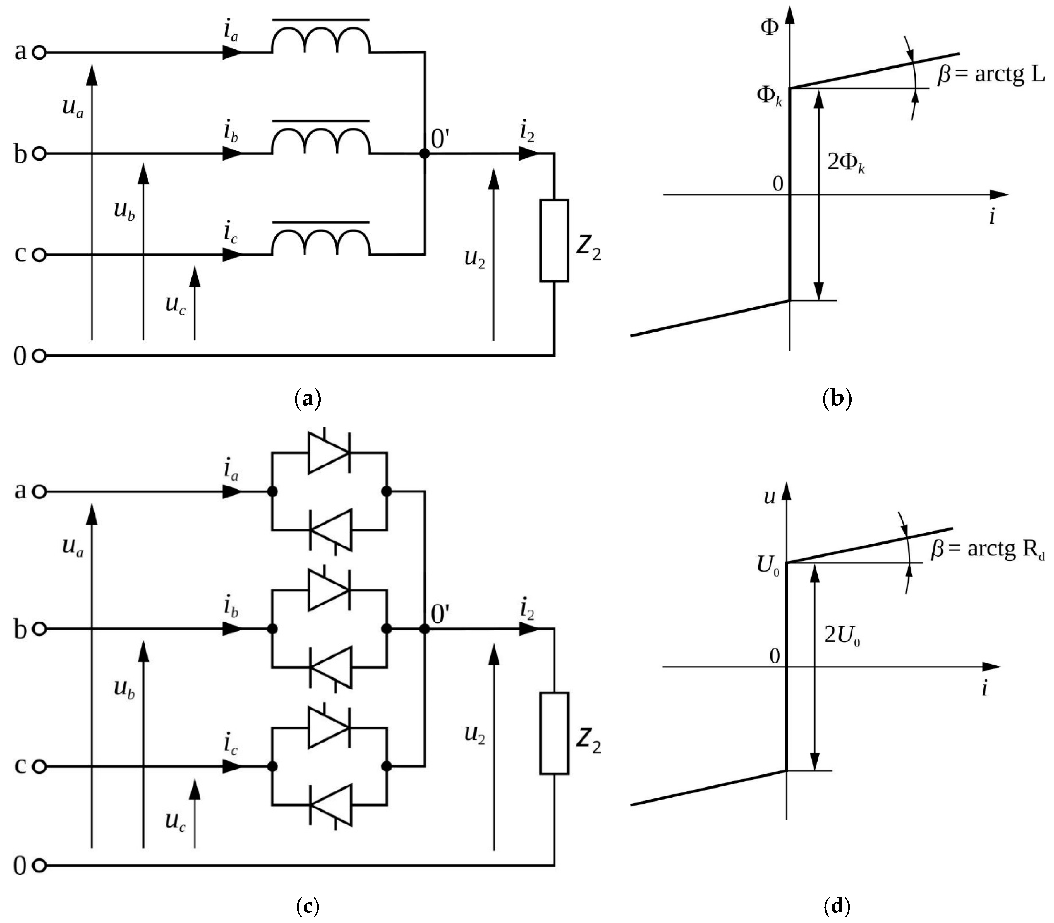
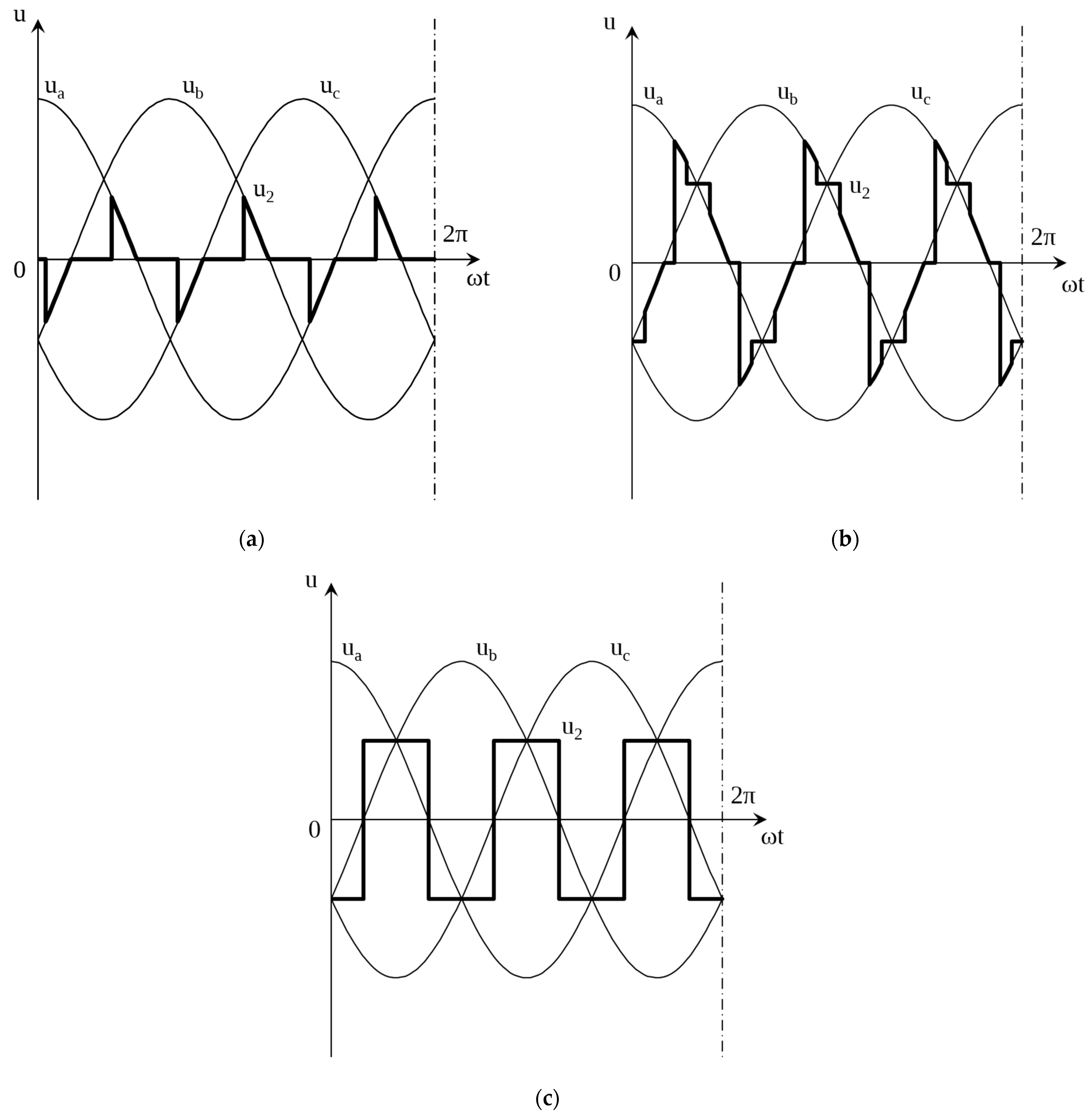
3.1. Generation of Higher Harmonics

Higher voltage harmonics can be generated in the VFC due to the non-linearity of magnetic and semiconductor elements (Figure 6). High-frequency PR supply voltage can improve the homogeneity of DBDs, decrease the operating voltage and maintain the same efficiency of the plasma process, which depends on the voltage, frequency and power losses in the VFC, high-voltage transformer and DBD PR.
For the block diagram presented in Figure 5, assuming that x i n t = X ^ i n cos ω t and x o u t t = X ^ o u t cos n ω t , where ω is the pulsation of the input signal, n = ω 2 / ω 1 —pulsation ratio of the output signal to the input signal and N = X ^ i n / X ^ o u t , the ratio of the input signal to the output signal amplitudes can be written as follows:
x o u t t = N X ^ i n cos n cos 1 x i n ( t ) X ^ i n = N X ^ i n T n x i n ( t ) X ^ i n ,
where T n x i n ( t ) X ^ i n is a Chebyshev polynomial of the first kind of order n. Therefore, the transformation function S(xin) of the VFC (Figure 4) can be presented as follows:
S x i n = N X ^ i n T n x i n t X ^ i n .
The Chebyshev polynomial of the first kind of order n can be represented as a series of functions x = x i n ( t ) X ^ i n of the following form:
T n x = x n n 2 x n 2 1 x 2 + n 4 x n 4 1 x 2 2 = k = 0 1 2 n n !   x n 2 k x 2 1 k 2 k ! .
In the case of the VFC, for which the output frequency is three times greater than the input (n = 3), the Chebyshev polynomial has the following form:
T 3 x = x 3 3 x 1 x 2 = 4 x 3 3 x .
Therefore, to get a frequency at the VFC output three times higher than the input frequency, the transforming function must be described by a third-order Chebyshev polynomial. Static VFCs are often blocks with n-inputs and one output. In converters with a symmetrical input (e.g., 3-phase, 6-phase), taking into account the presence of other phases, such converters are considered quads with input u1(t) and output u2(t). Assuming that the quantities at the input and output of the quadrant change cosine, and expressing the input current and voltage and the output current and voltage as follows:
u 1 t = U ^ 1 cos ω 1 t φ u 1 ,         i 1 t = I ^ 1 cos ω 1 t φ i 1 ,    
u 2 t = U ^ 2 cos ω 2 t φ u 2 ,         i 2 t = I ^ 2 cos ω 2 t φ i 2 ,    
where ω 2 ω 1 = n —frequency multiples; U ^ 1 , I ^ 1 , U ^ 2 , I ^ 2 —amplitude of signals at the input and output of the quadruple.
Such a quadruple can be described by the following six functions, relating currents and voltages at the input and output and their inverses:
u 1 i 1                                                                                   u 1 u 2                         u 1 i 2 u 2 i 2                                                                                   i 1 i 1                           u 2 i 1 linear functions                           non-linear functions (Chebyshev)
The input and output voltages, depending on the input and output currents, are linear functions. The remaining functions determining the input and output quantities are non-linear. If the input and output quantities are out of phase and their vectors intersect at the angle φ, then expression (6) for the transforming function S(xin), in accordance with the superposition principle, takes the following form:
S x i n = N X ^ i n k 1 φ T n x i n t X ^ i n + k 2 φ T n x i n t X ^ i n ,
where k 1 φ = cos φ , k 2 φ = sin φ , T n x i n t X ^ i n —Chebyshev polynomial of the first kind of order n, T n x i n t X ^ i n —Chebyshev polynomial of the second kind of order n.
As an example, Figure 6 presents two diagrams of a magnetic and thyristor VFC for n = 3, along with an approximation of the magnetisation characteristics ϕ = f(i) of a non-linear choke Ln = f(ϕ) and the current-voltage characteristics u = f(i) of push–pull connected thyristors.
The magnetic and thyristor VFCs presented in Figure 6a,c, together with their approximate current-voltage characteristics 6b and 6d, allow for the derivation of simplified relationships for the output voltage u2(t) depending on the amplitude Um of phase primary-side voltage u1(t). For this purpose, the voltage–current characteristics of both VFCs from Figure 6 were approximated with Equations (9b) and (9c) according to the following:
ω Φ = ω Φ k + ω L i t     f o r     i t > 0 ,                         u ( t ) = U 0 + R d i t           f o r     i t > 0
ω Φ = ω Φ k + ω L i t         for         i t < 0 ,             u t = U 0 + R d i t       for         i t < 0
where ω = 2 π f 1 —angular frequency of the primary supply voltage u1(t).
In the case of the choke, the phenomena of magnetic hysteresis and eddy currents were omitted, and in the case of the thyristors, only the conduction resistance was taken into account, omitting other parasitic elements. The operation of the VFC is determined by the ratio of the amplitudes of the supply voltage Um and the voltage U0 ( U k = ω Φ k for choke) at which the VFC system enters the conducting state ν. There is a full analogy here of a saturated magnetic circuit and a transistor in the following conducting state:   ν = U m U k or ν = U m U 0 . Depending on the value of ν , the VFC has three types of operation conditions (Figure 7):
-
In each phase, one magnetic or thyristor switch is in the conducting state, ν 1 , Figure 7a,
-
Magnetic or thyristor switches in two phases are in the conducting state for part of period ν 1 ,  Figure 7b,
-
In each phase of the three-phase circuit, three thyristors (magnetic switches) are conducting for part of the period equal to π/6, ν > 1 ,  Figure 7c.
Using the analogy to thyristor firing angle α (entry angle into the conducting state) for both the VFC configurations shown in Figure 6, its values can be determined as zeros of the Chebyshev polynomial for n = 3 (omitting harmonics 9, 15, etc.), according to Equation (8):
T 3 cos α = 4 cos α 3 3 cos α = 0 .
The zeros of this polynomial are cos ω t 1 = 0   a n d   cos ω t 2,3 = ± 3 2 , which gives the following numerical values of the angle α:
  • α 1 = ω t 1 = π 2 + k π —the threshold angle for entering the conducting state U m U o = ν = 1 Figure 7a,
  • α 2,3 = ± π 6 + 2 k π —the optimal angle for entering the conducting state—Figure 7c.
To determine the output voltage u2(t) for the optimal angle for entering the conducting state α = π/6, the rectangular waveform of this voltage from Figure 7c should be decomposed into a Fourier series consisting of odd harmonics that are multiples of 3. After calculating the Fourier series coefficients, we obtain the following:
u 2 t = 4 π U ^ 2 cos 3 ω t + 1 3 cos 9 ω t + 1 5 cos 15 ω t + ,
where: U ^ 2 —the amplitude of the 3rd harmonic of the output voltage.
In the no-load state, if the VFC is operating near the conduction transition point when U m U o > 1   b u t 1 , then the amplitude of the 3rd voltage harmonic is equal to the amplitude of the supply voltage U ^ 2 = U m . Then, we calculate U ^ 2 as the average value for the period of the rectangular waveform according to the following:
U ^ 2 = 3 π   π 6 π 2 U m cos 3 ω t d ω t = 2 π U m .
Taking into account Equation (11), we can write the instantaneous value of the secondary voltage of the VFC expressed by Equation (10) as follows:
u 2 t = 12 π 2 U m cos 3 ω t + 1 3 cos 9 ω t + 1 5 cos 15 ω t + .
If we assume that the choke and thyristor are ideal switches (L = 0 and Rd = 0), then the relationship (12) would be valid for the resistive load condition, assuming that the capacitance and inductance of the output circuit are tuned for n = 3 to a frequency of 150 Hz. The angle of inclination β of the approximated characteristics—Figure 6b,d, causes, as the VFC is loaded, a decrease in the amplitude of the 3rd harmonic of voltage in relation to the fundamental harmonic; therefore, in relation (12) in the case of loading, we should take into account the ratio of the third U ^ 3 h to the first U ^ 1 h harmonic of phase primary voltage ( U ^ 3 h U ^ 1 h ).

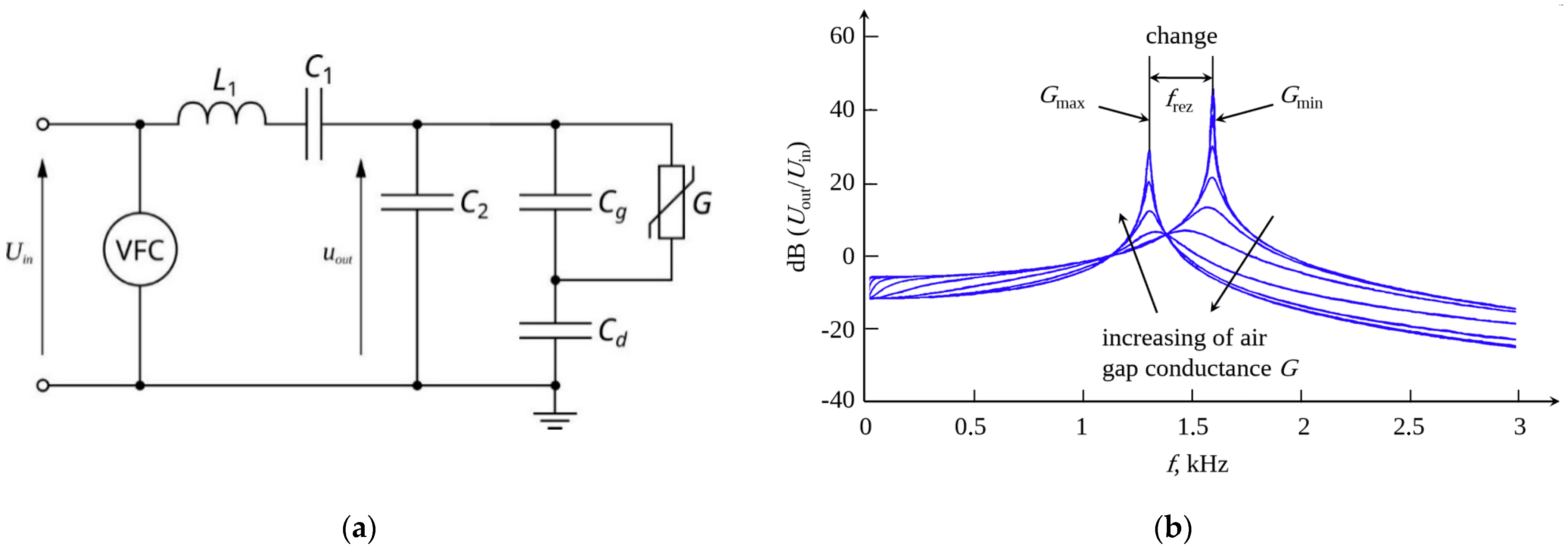
3.2. Resonance Phenomenon

The PR with DBD provides a capacitive load for the PSS, which naturally forms a freely oscillating resonant circuit with VFC inductive elements. The linear resonance phenomenon can occur in a series or parallel LC circuit. Different solutions for VFC resonant topologies can be found in the literature [40,41,42,43].
A topology often used to drive DBD PR is the series resonant circuit, in which the resultant capacitance Cr of the PR oscillates freely with the additional inductance L1 and/or the dissipation inductance of the high-voltage transformer. As studies have shown [42], a disadvantage of the series inverter is that it makes it difficult to meet the transistor switching condition at zero current since changes in the conductance of the gap have a large effect on the resonant frequency of the converter. Furthermore, in the event of a short circuit, there is a large increase in the circuit current and a loss of resonance, which can result in the destruction of the transistors. The best performance is shown by resonant inverter (RI) topologies with an additional capacitor C2 connected in parallel to the PR terminals (LCC topology) and the series-parallel topology, with capacitor C1 connected in series to inductance L1 and additional inductance L2 connected in parallel to the PR terminals (LLC topology). The main advantages of the LCC and LLC topologies are that the conductance of the air gap G has little effect on the resonant frequency, RI has better short-circuit resistance, and the transistors switch easily at zero current [41,43].
Figure 8a shows an example of the LCC topology of a converter in which an additional capacitor C2 is connected in parallel to the plasma reactor with resultant capacitance C r , where C r = C d C g C d + C g ,   C d —capacitance of DB and C g —capacitance of discharge gap. The amplitude characteristics of the LCC circuit presented in Figure 8b show that changes in the conductance of the air gap of the DBD PR, in which the discharges take place, from very small values Gmin to very large Gmax, cause a relatively small change in the converter’s resonance frequency (for the analysed circuit, going from approximately 1.1 kHz to 1.6 kHz). The short-circuit condition does not interrupt the resonant nature of the converter’s operation, which favours the stabilisation of the DBD.
The transistor inverter in the LCC topology presented in Figure 8a is used to power discharge lamps. It is characterised by the least sensitivity to changes in air gap conductance G and natural resistance to short circuits. To ensure zero-current commutation, each of the series and series-parallel topologies requires precise measurement of the instantaneous value of the current to accurately synchronise the switching of the transistors with the varying resonant frequency [42].

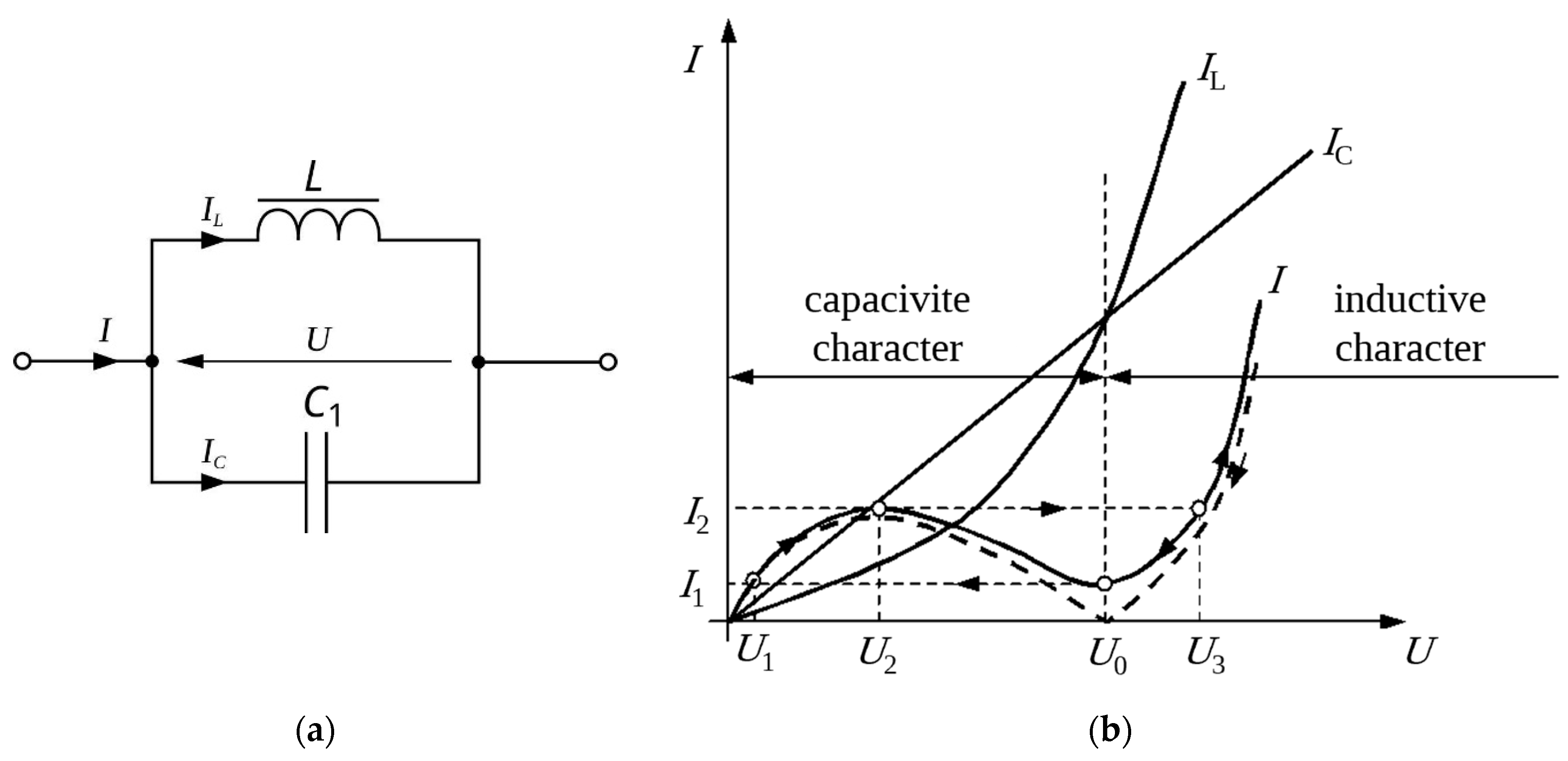
3.3. Phenomena of Ferroresonance

Plasma reactor power supplies with ferromagnetic elements (magnetic switches, high-voltage transformers) typically operate near saturation of the non-linear current-voltage characteristics of the coil cores, as described in Section 3.1 and Section 4.1. In such power supplies, it becomes necessary to compensate for reactive inductive power by means of capacitors, which can result in ferroresonance (FR) phenomena in a system of a non-linear core inductor (magnetic switch) and a linear capacitor connected in series (voltage ferroresonance, UFR) or in parallel (current ferroresonance, IFR). The current-voltage characteristics of the IFR and UFR have a different waveform with current excitation and a different waveform with voltage excitation. Figure 9 shows the current ferroresonance phenomenon when forced from a sinusoidal current source. IFR occurs in a parallel LC circuit when the RMS values of the first harmonic currents in capacitor IC and in non-linear inductor IL are equal to the voltage U0. The instantaneous values of both currents are distorted and contain higher harmonics so that the RMS value of the current on the I(U) characteristic, for U = U0, does not reach zero and is slightly higher than the ideal characteristic, indicated in Figure 9b by the dashed line. When, in the circuit in Figure 9a, the RMS value of the supply current slowly increases, starting from zero, there is a sharp jump in the RMS value of the voltage U from U2 to U3 at a certain value I = I2. This causes a simultaneous jump in the RMS value of the individual component currents IL and IC, whereby, before the jump, the value of IL was less than IC and after the jump, IL > IC, indicating a rapid change in the nature of the connection from capacitive to inductive. The FR state (I = min) is not reached in the process, and stable system operation supplied by the current source is not possible.
The course of the phenomena will be slightly different if the system in Figure 9a is supplied from a voltage source and the RMS value of U is increased or decreased. In this case, no jumps in the value of U are observed. Increasing the value of U from zero initially increases the value of I, but for U > U2, the value of I begins to decrease. For U = U0, the I value reaches a minimum (IFR). A further increase in U causes I to increase again.
In the case of UFR, which occurs in the series connection of a linear capacitor and a non-linear inductor, with voltage excitation, there are step changes in RMS value and in the nature of the circuit from inductive to capacitive, whereas, with current excitation, there are no step changes in I and the U(I) characteristic can be determined experimentally.
In the presented analysis, the possibility of sub-harmonics (slow oscillations), which further complicate the analysis of ferro-resonant phenomena, has been ignored.
In a PSS PR with GAD, both types of FR can occur between the non-linear reactance of the cores of the primary and secondary coils, operating at magnetic flux saturation, and the linear capacitors.
It should be noted that both ferro-resonant phenomena are dynamic and cause sudden changes in voltage (at IFR) and current (at UFR) called FR oscillations. These can cause a variety of effects, not necessarily beneficial, on the operation of the power supplies themselves and also on the electrical network from which they are supplied, reducing the reliability of operation and the quality of the power supply as a result of interruptions associated with PSS shutdown (overvoltage at IFR and overcurrent at UFR) and distortion of the voltage and current waveforms.
The GAD PR requires a power source with an adjustable electrode current because the voltage between the PR electrodes after ignition drops to a value several times lower than the ignition voltage and, depending on the working gas, remains constant, as can be observed in the static voltage–current characteristics of the GAD shown in Figure 3d (Section 2.2). Therefore, the only possibility to regulate the PR power from the GAD is to regulate the electrode current, which should be limited to a few amperes to ensure the generation of a non-thermal plasma while maintaining a relatively high voltage, which largely depends on the flow rate of the working gas, its type, the geometry of the electrodes (length, angle, number of electrodes) and the parameters of the power system. An example of a PSS for PR using the FR phenomenon is presented in Section 4.3.

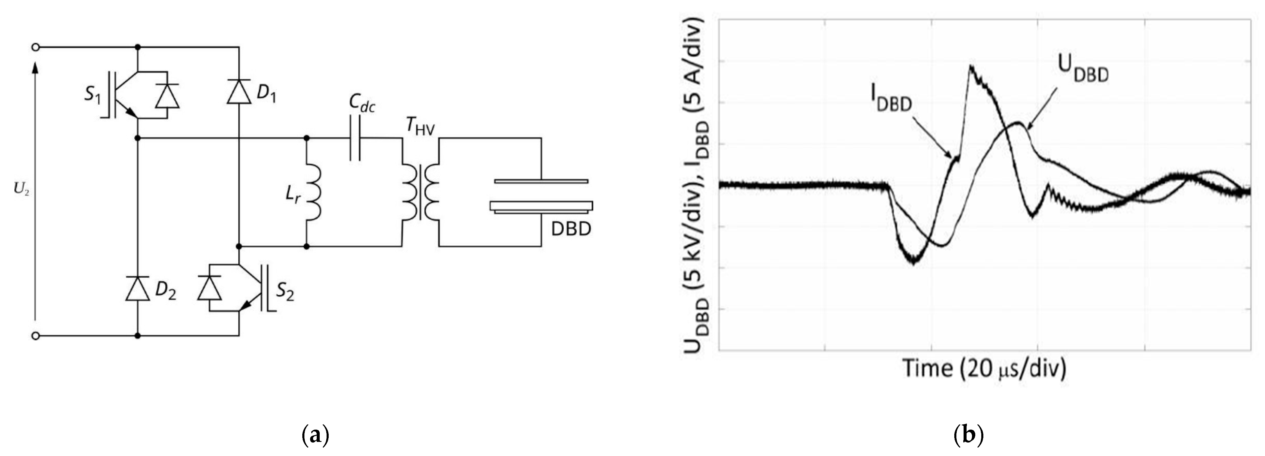
3.4. Pulsed Power Energy and the Phenomenon of SOs in PPS

There are widespread trends that can be observed in the implementation of pulsed power systems for the generation of APCPs [9,35,36,37,44]. Pulsed power supplies (PPS) enable stable discharge conditions at high pressure and low temperature. This applies to reactors with DBS, GADs and APPJs in the presence or absence of a dielectric barrier, as discussed in Section 2.
In DBD reactors for ozone generation, the processes of ionisation and dissociation of oxygen and nitrogen (for discharges in air) take tens to hundreds of nanoseconds, whereas the processes of ozone formation and its diffusion from the discharge gap into the medium to be sterilised and/or disinfected are 103 to 106 times slower and are micro and milliseconds, respectively. Therefore, the pulse frequency of the supply voltage should be around 1000 Hz, and the pulse width should be in the order of hundreds of nanoseconds so that the O3 formed during the recombination process leaves the discharge gap and does not decompose into oxygen. This occurs at sinusoidal voltage, where energy is supplied to the discharge gap for the entire voltage period, reducing the efficiency of the ozone generation process.
Plasma reactors with GADs, both single and multi-electrode, as well as APPJs with and without DBs, also benefit from pulsed energy to power them. In a two-electrode PR with a micro-gliding arc discharge (μGAD or APPJ), supplied with an AC voltage with a frequency in the range of 10–20 kHz, the GAD discharge has slightly different characteristics than with a mains frequency sinusoidal voltage [45]. Relatively short millisecond voltage periods do not allow the discharge to turn into a short-circuit arc, which makes it easier to maintain the state of thermodynamic imbalance than at the network frequency voltage. In addition, the PPS provide extensive options for controlling the current and voltage of the GAD PR.
The GAD plasma reactor is a non-linear power receiver with special requirements for the PPS. Firstly, the power supply must generate a high voltage, adapted primarily to the type of process gas and the distance of the electrodes in the ignition zone, so that the discharge in the process gas can ignite cyclically without additional ignition electrodes or pre-ionisation. Secondly, from the receiver’s point of view, it is advantageous for the power supply to have the characteristics of a regulated current source. Therefore, the PPS source should quickly and efficiently limit the current μGAD, which then maintains a stable glow discharge. These PPS features can be achieved by combining a number of standard and non-standard power conversion techniques in pulse inverters.
Section 4.4 and Section 4 provide an example of a pulsed power system for a two-electrode plasma reactor of the μGAD or APPJ type, which exploits the parasitic phenomenon of commutation overvoltage to improve the ignition performance of these reactors.

4. Examples of APCP Reactor Power Supply Systems

4.1. PSS of PR Using Higher Harmonics

The higher harmonic voltages generated in a PSS due to the non-linearity of its magnetic and semiconductor components can be used to improve the performance of PRs from DBDs as well as from GADs, in particular in terms of the ignition of the discharge, its uniformity and the efficiency of the plasma process. Figure 10 shows two exemplary PSS solutions dedicated to PR with DBD and GAD. Higher odd harmonics are, with sinusoidal excitation, generated in the phase voltages on the primary side of the PSS (Figure 10a) or in the star-connected primary and secondary windings of single-phase transformers (Figure 10b).
In the VFC system for the DBD PR, the third harmonic voltage, dominant in the single-phase FC output (between the FC star connection and the PEN) (Figure 10a), is applied to the terminals of the high-voltage transformer HV Tr. A three-times-higher supply frequency (150 Hz) reduces the supply voltage amplitude U ^ o u t to a value of approx. 0.64Um at 50 Hz).
In the GAD PSS (Figure 10b), the higher harmonics are used to assist GA ignition, significantly reducing the zero-current interruptions each time the electrode current value passes zero. Furthermore, the output voltage Uout of the three single-phase transformers can be significantly lower than the ignition voltage Uign at the output of the ignition transformer. This means that the single-phase transformers, connected on their primary and secondary sides in the star supplying the GAD electrodes, can be designed for voltages several times lower than the ignition voltage and smaller transformer dimensions [19,20,40].

4.2. PSS of PR Using Resonance Phenomena

As an example of the application of resonance phenomena in PSS, the diagonal bridge resonant converter for the excitation of the DBD reactor used in a diesel engine exhaust treatment system has been presented in Figure 11, together with courses of the current and voltage of a DBD reactor energised by this system. Changes in the capacity of the reactor substantially affect the resonant frequency of the resonant circuit and, as a result, the operation of the VFC. The overall efficiency of the PSS, including the efficiency of the resonant converter and HV transformer, was 68% [41].
The PSS efficiency shown in Figure 12b was calculated from active power measurements at the inputs of the resonant converter and high-voltage transformer, respectively, using a Fluke NORMA 5000 power analyser with an ISM 50/10 current shunt (S/N 4878, 9.994 mΩ, 200 MHz). DBD PR active power calculations were performed on a Lissajous curve using a WaveRunner 6100 digital oscilloscope (LeCroy). The Lissajous curve was obtained by applying a signal proportional to the charge from a 1 microfarad capacitor connected in series with the discharge gap to the horizontal deflection terminals and a voltage signal to the vertical deflection terminals of the oscilloscope.
The VFC for the APPJ with DB is shown in Figure 13. The APPJ is represented by a series combination of capacitance and resistance, and the resonant oscillating circuit is formed by the capacitance of the dielectric layer Cd and the inductance of the secondary circuit of the high-voltage transformer Lcoil, energised by a sinusoidal RF frequency signal. The RF PSS provides the appropriate voltage and power necessary to maintain stable plasma process parameters. The output characteristic of the sine wave generator is similar to that of the real 50 Ω output impedance power source, and the receiver impedance (APPJ) must be adjusted to maintain the appropriate plasma process parameters.

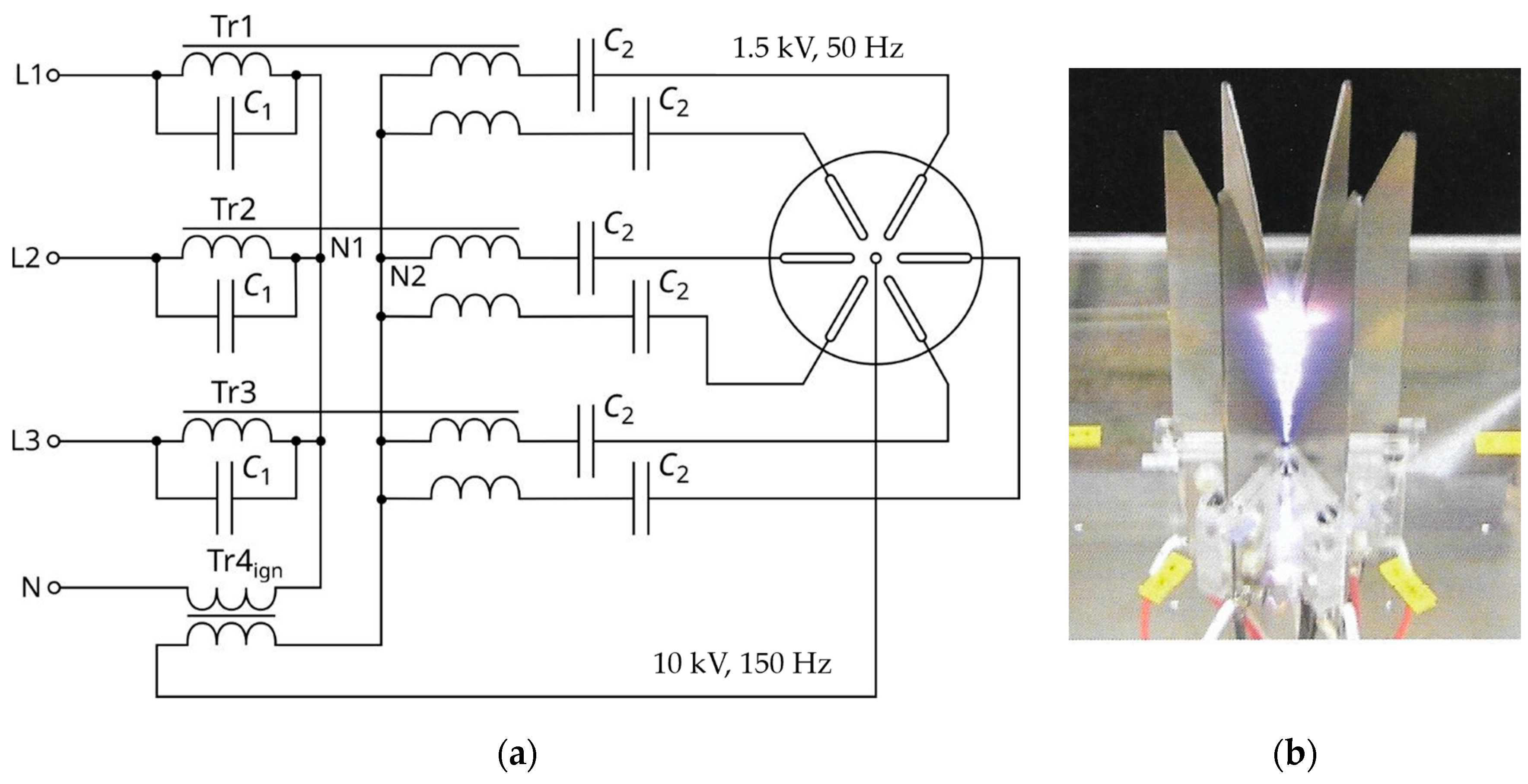
4.3. PSS of PR Using IFR and UFR Phenomena

An example of a 6-electrode PSS GAD PR design consisting of 3 single-phase high-voltage transformers with six secondary windings and an ignition electrode that uses both IFR phenomena on the primary side of the PSS and UFR phenomena on the secondary side of the PSS is shown in Figure 14.
On the primary side of the star-connected transformers, capacitors C1 are connected in parallel with each phase coil core to form IFR circuits, while capacitors C2 are connected in series with the six coil cores on the secondary side of the transformers to form UFR circuits. During the IFR phenomenon, the current on the primary side of the high-voltage transformer (HVT) is limited by the low resistance of the coil core windings, while on the secondary side of the HVT, the voltage between the GAD PR electrodes increases due to the UFR phenomenon.
As mentioned in Section 3.3, in order to avoid the disadvantageous effects of current and voltage oscillations during ferroresonance, both the GAD PR parameters (geometry, including discharge zone volume, gas type and flow rate) and, above all, the PSS parameters (voltage, power, frequency, energy efficiency and plasma-chemical process yield) must be carefully selected. The use of IFR and UFR phenomena allows the energy efficiency of the PSS GAD to be improved, enabling both a significant reduction in the PSS primary-side current and an increase in the interelectrode voltage on the secondary side of high-voltage transformers.
The paper [17] presents the results of toluene decomposition in a GAD reactor with a conical chamber and six electrodes. The electrodes were supplied by six single-phase transformers controlled by transistor converters. Ferroresonance occurred in a system of high-voltage capacitors and non-linear inductances resulting from the increased magnetic flux caused by shunting the main flux of the high-voltage transformers.
A controlled transistor inverter enabled the current of the GAD PR electrodes to be regulated and a high degree of power utilisation to be achieved. At the output of each transformer, the voltage supplied to the electrodes was adjustable between 1000 V and 2000 V, and the voltage ratio of each of the six single-phase transformers was 230/2100 V. The authors in [17] did not provide an FR-based VFC wiring diagram in their article, so it is difficult to verify which type of FR they used in the power supply, be it IFR or UFR, or perhaps both.
Apart from the publication in question, no other items concerning power systems based on the FR phenomenon were found in the literature. In our opinion, the use of IFR and UFR phenomena may improve the energy efficiency of the PSS GAD, as well as reduce the PSS current on its primary side and increase the interelectrode voltage on the secondary side of the PSS. This requires in-depth analysis and modelling to avoid the side- effects of FR phenomena mentioned in Section 3.3, especially in the design of industrial installations.

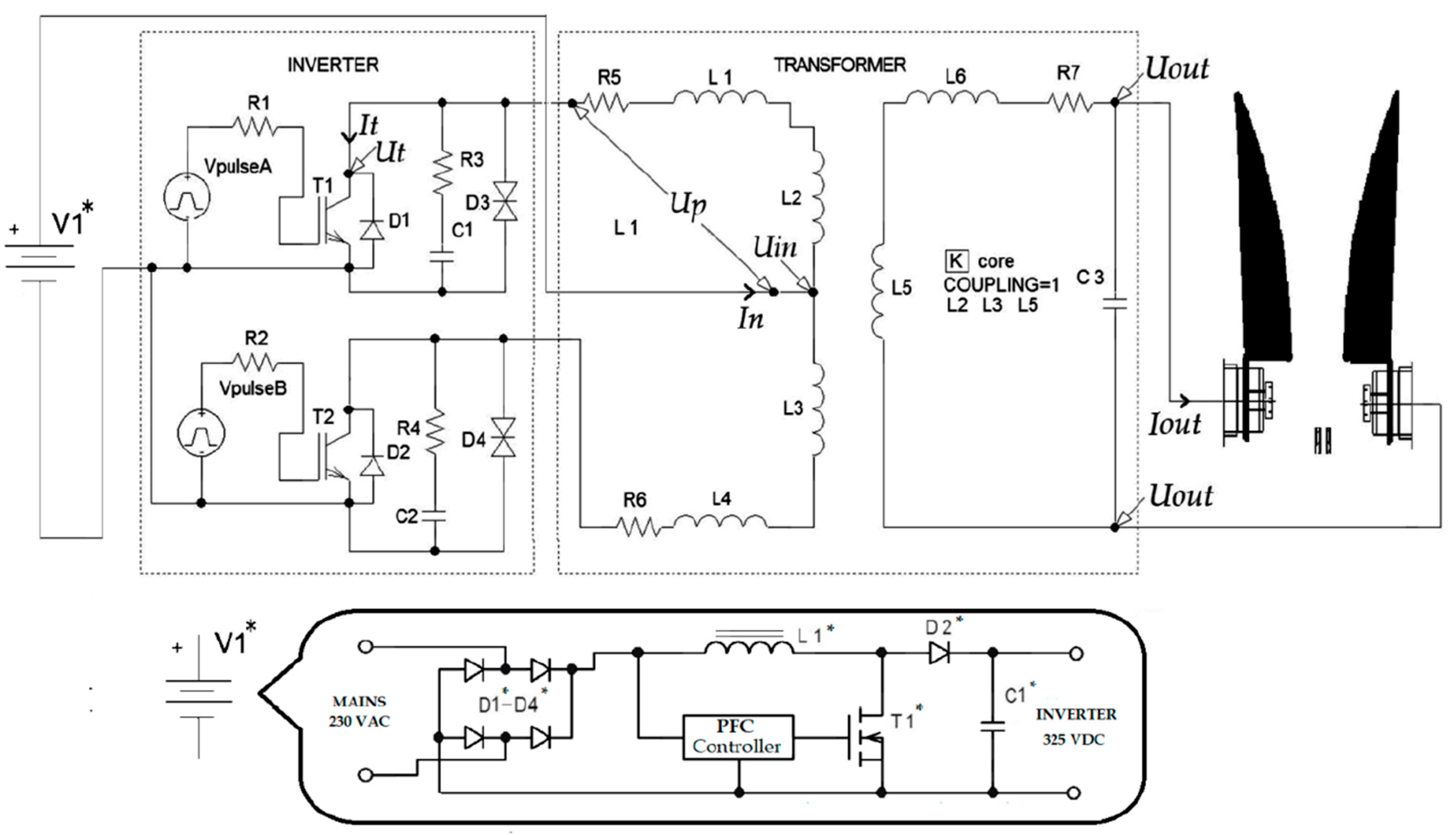
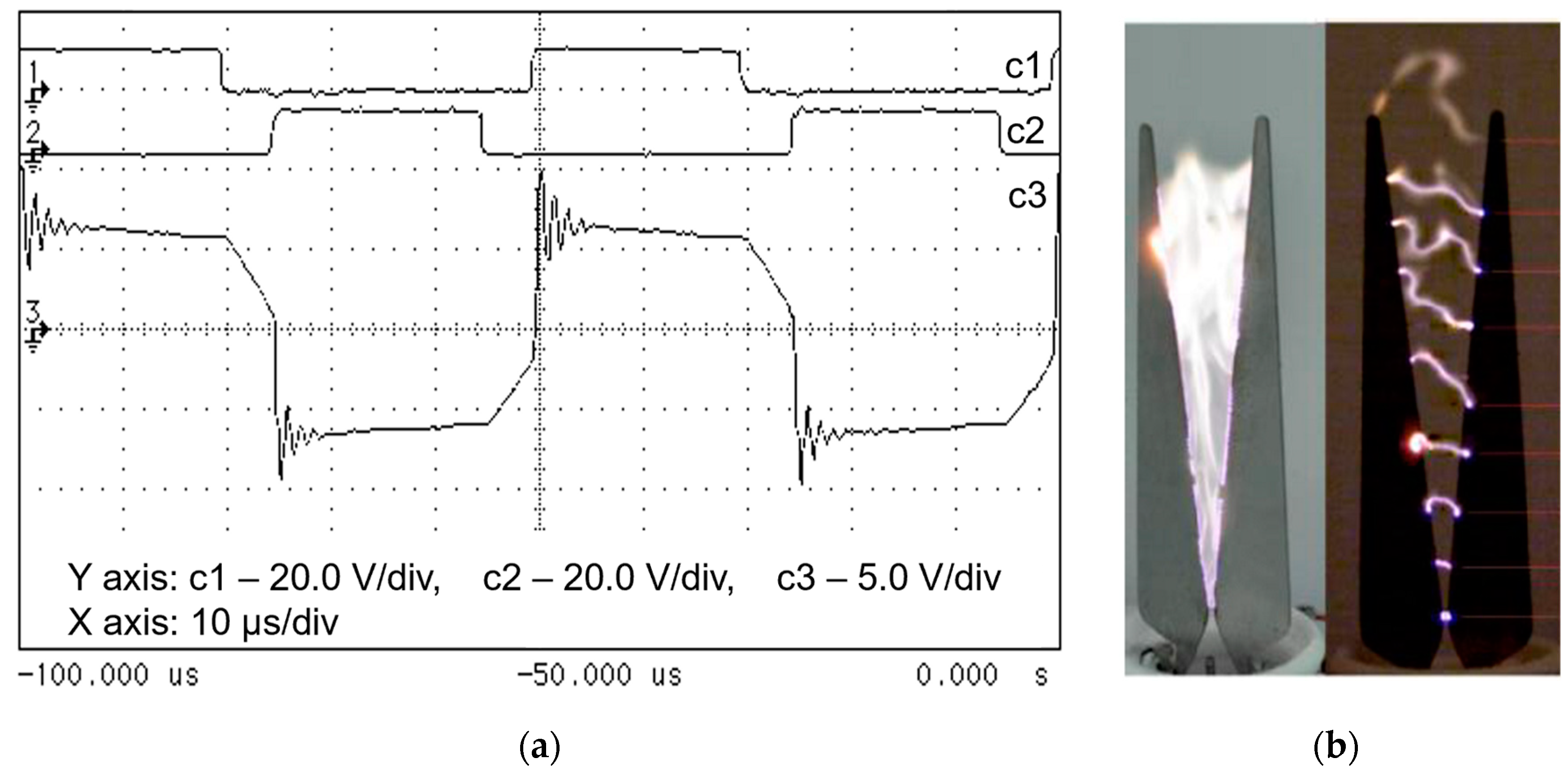
4.4. PSS of PR Using Pulsed Power and the Phenomenon of SOs

The push–pull PPS was used to take advantage of the parasitic phenomenon of commutation overvoltage and thus improve the ignition parameters in the micro-gliding arc discharge reactor (μGAD). To describe the use of parasitic phenomena during energy conversion, a simplified diagram of this system is outlined in Figure 15. The input side of the power supply is standard for PPS devices and has an input rectifier and filtering capacitors. There is also a power factor correction (PFC) controller and a system for pre-charging capacitors. In this way, DC voltage is prepared to supply the push–pull topology converter. These are solutions that are treated as standard in pulse technology and do not differ in this APCP power supply.
As can be seen in Figure 15, the positive pole of the filtered DC voltage V 1 * is applied to the central tap in the primary winding. Potential 0 is alternately connected to the start and end of the winding according to the frequency and period of the pulse. The executive switches are insulated-gate bipolar transistors (IGBTs) labelled T1 and T2, coils L2, L3 and L5 are magnetically coupled, and coils L1, L4, and L6 represent leakage inductances, as shown in the equivalent diagram.
During pulse repetition, a rapidly varying current is conducted through the rising edge to the magnetically coupled transformer coils. The rapid current changes strongly depend on the leakage inductance. This is crucial because of the SOs generated during current changes. Essentially, they are used to generate high-voltage pulses (HVPs) to support the ignition of the plasma reactor. The formation of SOs can be seen in Figure 16a, which, at idle on one coil of the secondary winding and during operation with air as the process gas, completely eliminates the need for additional ignition systems. The discharge of the two knife-shaped μGAD electrodes in the ignition space at atmospheric pressure is shown in Figure 16b.

5. Conclusions

Reactors for the production of APCPs are non-linear power loads using different types of electrical discharge. Their power systems must meet specific requirements. These include the need to ensure high efficiency of the plasma process, ignition of the discharges, homogeneity of the DBD discharges to avoid arcing and spark discharges that reduce the efficiency of the generation of ozone and other active plasma particles and, in the case of GADs, to ensure non-thermal glow discharge conditions, with the high voltage and relatively low current of the electrodes and their cyclic operation after ignition without current-less interruptions.
Depending on the type of electrical discharge, the performance of plasma reactors can be controlled by voltage, current, and frequency. PRs with discharges in the presence of DBs are non-linear capacitive-resistive receivers requiring a high voltage and increased or high frequency supply and should be powered by voltage sources, while GAD and APPJ PRs without DBs, which are non-linear resistive receivers, require current sources to power them.
Non-linear phenomena occurring in plasma reactor power systems such as harmonic generation, resonance and FR, and SO, which are very often considered as their disadvantage, can support the operation of a plasma reactor with DBD, GAD, and APPJ in order to achieve greater discharge uniformity and thus non-thermal and non-equilibrium plasma conditions without sparks, the possibility to reduce the high voltage on the DBD discharge elements due to an increase in the PSS frequency, to provide a reliable ignition of the GAD depending on the type of working gas, and, very importantly, to increase the efficiency of the PSS and the plasma-chemical processes as a whole.
Appropriate modifications known for years—PPS with push–pull topology—allow for the implementation of this atypical solution to supply μGAD. The main disadvantages of the topology are used here as advantages. SOs, as parasitic parameters of PSS with push–pull topology, allow the effective generation of μGADs, which is very important in the condition of air as plasma gas. Thanks to them, there is no need to use any additional ignition sources, and as much as a 60% increase in voltage for ignition in the air can be observed.

Author Contributions

Conceptualisation, H.D.S., G.K.K. and O.B.; methodology, G.K.K. and O.B.; validation, G.K.K., H.D.S. and O.B.; formal analysis, G.K.K.; investigation, H.D.S., G.K.K. and O.B.; resources, H.D.S.; data curation—G.K.K. and O.B.; writing—original draft preparation, H.D.S. and G.K.K.; writing—review and editing, G.K.K. and O.B.; visualisation, G.K.K.; supervision, G.K.K. and H.D.S. All authors have read and agreed to the published version of the manuscript.

Funding

This research was funded by Lublin University of Technology grants numbers FD 20/EE-2/416, FD-20/EE-2/406 FD-20/EE-2/401 and 5/GnG/2022 intended for research activities within the “Automatics, Electronics and Electrical Engineering” scientific discipline.

Data Availability Statement

The data that support the findings of this study are available from the corresponding author upon reasonable request.

Conflicts of Interest

The authors declare no conflicts of interest.

References

  1. Stryczewska, H.D.; Boiko, O.; Stępień, M.A.; Lasek, P.; Yamazato, M.; Higa, A. Selected Materials and Technologies for Electrical Energy Sector. Energies 2023, 16, 4543. [Google Scholar] [CrossRef]
  2. Li, S.R.; Ongis, M.; Manzolin, G.; Gallucci, F. Non-thermal plasma-assisted capture and conversion of CO2. Chem. Eng. J. 2021, 410, 128335. [Google Scholar] [CrossRef]
  3. Barkhordari, A.; Karimian, S.; Rodero, A.; Krawczyk, D.A.; Iman Mirzaei, S.I.; Falahat, A. Carbon Dioxide Decomposition by a Parallel-Plate Plasma Reactor: Experiments and 2-D Modelling. Appl. Sci. 2021, 11, 10047. [Google Scholar] [CrossRef]
  4. Bárdos, L.; Baránková, H. Cold atmospheric plasma: Sources, processes, and applications. Thin Solid Films 2010, 518, 6705–6713. [Google Scholar] [CrossRef]
  5. Cretu, D.; Burlică, R.; Astanei, D.; Dirlău, J.-D.; Beniugă, O. Energy efficiency evaluation of HV power supplies for non-thermal plasma generation. In Proceedings of the 8th International Conference on Modern Power Systems (MPS), Cluj-Napoca, Romania, 21–23 May 2019. [Google Scholar]
  6. Fanellia, F.; Fracassi, F. Atmospheric pressure non-equilibrium plasma jet technology: General features, specificities and applications in surface processing of materials. Surf. Coat. Technol. 2017, 322, 174–201. [Google Scholar] [CrossRef]
  7. Mohapatro, S.; Rajanikanth, B.S. A core study on NOx removal in diesel exhaust by pulsed/AC/DC electric discharge plasma. In Proceedings of the IEEE 2011 International Conference on Power and Energy Systems (ICPS), Chennai, India, 22–24 December 2011; IEEE Explore Digital Library: New York, NY, USA, 2011; pp. 1–6. [Google Scholar]
  8. Massines, F.; Sarra-Bournet, C.; Fanelli, F.; Naudé, N.; Gherardi, N. Atmospheric pressure low temperature direct plasma technology: Status and challenges for thin film deposition. Plasma Process. Polym. 2012, 9, 1041–1073. [Google Scholar] [CrossRef]
  9. Wedaa, H.; Abdel-Salam, M.; Ahmed, A.; Mizuno, A. NO removal using dielectric barrier discharges in a multirod reactor stressed by AC and pulsed high voltages. IEEE Trans. Dielectr. Electr. Insul. 2011, 18, 1743–1751. [Google Scholar] [CrossRef]
  10. Eliasson, B.; Hirth, M.; Kogelschatz, U. Ozone synthesis from oxygen in dielectric barrier discharges. J. Phys. D Appl. Phys. 1987, 20, 1421. [Google Scholar] [CrossRef]
  11. Eliasson, B.; Kogelschatz, U. Modelling and applications of silent discharge plasmas. IEEE Trans. Plasma Sci. 1991, 19, 309–323. [Google Scholar] [CrossRef]
  12. Matsumoto, T.; Wang, D.; Namihira, T.; Akiyama, H. Performances of 2 nanoseconds pulsed discharge plasma. Jpn. J. Appl. Phys. 2011, 50, 08JF14. [Google Scholar] [CrossRef]
  13. Akiyama, H.; Sakugawa, T.; Namihira, T.; Takaki, K.; Minamitani, Y.; Shimomura, N. Industrial applications of pulsed power technology. IEEE Trans. Dielectr. Electr. Insul. 2007, 14, 1051–1064. [Google Scholar] [CrossRef]
  14. Mohapatro, S.; Allamsetty, S.; Madhukar, A.; Sharma, N.K. Nanosecond pulse discharge based nitrogen oxides treatment using different electrode configurations. High Voltage 2017, 2, 60–68. [Google Scholar] [CrossRef]
  15. Liguori, A.; Pollicino, A.; Stancampiano, A.; Tarterini, F.; Focarete, M.L.; Colombo, V.; Gherardi, M. Deposition of plasma-polymerized polyacrylic acid coatings by a nonequilibrium atmospheric pressure nanopulsed plasma jet. Plasma Process. Polym. 2016, 13, 375–386. [Google Scholar] [CrossRef]
  16. Huiskamp, T.; Takamura, N.; Namihira, T.; Pemen, A.J.M. Matching a Nanosecond Pulse Source to a Streamer Corona Plasma Reactor with a DC Bias. IEEE Trans. Plasma Sci. 2015, 43, 617–624. [Google Scholar] [CrossRef]
  17. Młotek, M.; Reda, E.; Reszke, E.; Ulejczyk, B.; Krawczyk, K. A gliding discharge reactor supplied by a ferro-resonance system for liquid toluene decomposition. Chem. Eng. Res. Des. 2016, 111, 277–283. [Google Scholar] [CrossRef]
  18. Brasov Felea, I.C.; Hnatiuc, E.; Astanei, D. Characterization of cold plasma glidarc reactors. In Proceedings of the International Aegean Conference on Electrical Machines and Power Electronics (ACEMP) & International Conference on Optimization of Electrical and Electronic Equipment (OPTIM), Brasov, Romania, 2–3 September 2021. [Google Scholar]
  19. Komarzyniec, G.; Aftyka, M. Cooperation of the Plasma Reactor with a Converter Power Supply Equipped with a Transformer with Special Design. Energies 2023, 16, 6825. [Google Scholar] [CrossRef]
  20. Stryczewska, H.D. Supply Systems of Non-Thermal Plasma Reactors. Construction Review with Examples of Applications. Appl. Sci. 2020, 10, 3242. [Google Scholar] [CrossRef]
  21. Winter, J.; Brandenburg, R.; Weltmann, K.D. Atmospheric pressure plasma jets: An overview of devices and new directions. Plasma Sources Sci. Technol. 2015, 24, 064001. [Google Scholar] [CrossRef]
  22. Lu, X.; Laroussi, M.; Puech, V. On atmospheric-pressure non-equilibrium plasma jets and plasma bullets. Plasma Sources Sci. Technol. 2012, 21, 034005. [Google Scholar] [CrossRef]
  23. Chen, F.; Liu, S.; Liu, J.; Huang, S.; Xia, G.; Song, J.; Xu, W.; Sun, J.; Liu, X. Surface modification of tube inner wall by transferred atmospheric pressure plasma. Appl. Surf. Sci. 2016, 389, 967–976. [Google Scholar] [CrossRef]
  24. Guaitella, O.; Sobota, A. The impingement of a kHz helium atmospheric pressure plasma jet on a dielectric surface. J. Phys. D Appl. Phys. 2015, 48, 255202. [Google Scholar] [CrossRef]
  25. Wu, S.; Wang, Z.; Huang, Q.; Tan, X.; Lu, X.; Ostrikov, K. Atmospheric-pressure plasma jets: Effect of gas flow, active species, and snake-like bullet propagation. Phys. Plasmas 2013, 20, 023503. [Google Scholar] [CrossRef]
  26. Laroussi, M.; Akan, T. Arc-free atmospheric pressure cold plasma jets: A review. Plasma Process. Polym. 2007, 4, 777–788. [Google Scholar] [CrossRef]
  27. Stryczewska, H.D.; Stępień, M.A.; Boiko, O. Plasma and Superconductivity for the Sustainable Development of Energy and the Environment. Energies 2022, 15, 4092. [Google Scholar] [CrossRef]
  28. Foest, R.; Schmidt, M.; Becker, K. Microplasmas, an emerging field of low-temperature plasma science and technology. Int. J. Mass Spectrom. 2006, 248, 87–102. [Google Scholar] [CrossRef]
  29. Mariotti, D.; Sankaran, R.M. Microplasmas for nanomaterials synthesis. J. Phys. D Appl. Phys. 2010, 43, 323001. [Google Scholar] [CrossRef]
  30. Lin, L.; Wang, Q. Microplasma: A new generation of technology for functional nanomaterial synthesis. Plasma Chem. Plasma Process. 2015, 35, 925–962. [Google Scholar] [CrossRef]
  31. Fanelli, F.; Fracassi, F. Aerosol-assisted atmospheric pressure cold plasma deposition of organic–inorganic nanocomposite coatings. Plasma Chem. Plasma Process. 2014, 34, 473–487. [Google Scholar] [CrossRef]
  32. Mariotti, D.; Belmonte, T.; Benedikt, J.; Velusamy, T.; Jain, G.; Švrček, V. Low temperature atmospheric pressure plasma processes for ‘‘green’’ third generation photovoltaics. Plasma Process. Polym. 2016, 13, 70–90. [Google Scholar] [CrossRef]
  33. Babaeva, N.Y.; Kushner, M.J. Interaction of multiple atmospheric-pressure microplasma jets in small arrays: He/O2 into humid air. Plasma Sources Sci. Technol. 2014, 23, 015007. [Google Scholar] [CrossRef]
  34. Penkov, O.V.; Khadem, M.; Lim, W.S.; Kim, D.E. A review of recent applications of atmospheric pressure plasma jets for materials processing. J. Coat. Technol. Res. 2015, 12, 225–235. [Google Scholar] [CrossRef]
  35. Malik, M.A.; Schoenbach, K.H.; Abdel-Fattah, T.M.; Heller, R.; Jiang, C. Low Cost Compact Nanosecond Pulsed Plasma System for Environmental and Biomedical Applications. Plasma Chem. Plasma Process. 2017, 37, 59–76. [Google Scholar] [CrossRef]
  36. Koliadimas, A.; Apostolopoulos, D.; Svarnas, P.; Sklias, K.; Athanasopoulos, D.K.; Mitronikas, E.D. Micro-Processor Based Modular Pulsed High Voltage Power Supply for Driving Atmospheric-Pressure DBD Plasmas. IEEE Trans. Plasma Sci. 2019, 47, 1621–1628. [Google Scholar] [CrossRef]
  37. Tsai, M.T.; Ke, C.W. Design and implementation a high-voltage high-frequency pulse power generation system for plasma applications. In Proceedings of the 14th Power Electronic and Motion Control Conference, Wuhan, China, 17–20 May 2009; pp. 1556–1560. [Google Scholar]
  38. Yong-Nong, C.; Chih-Ming, K. Design of Plasma Generator Driven by High-frequency High-voltage Power Supply. J. Appl. Res. Technol. 2013, 11, 225–234. [Google Scholar] [CrossRef]
  39. Sánchez-Trujillo, A.B.; Martínez-Méndez, R.; Portillo-Rodríguez, O.; Vázquez-Guzman, G. Prototype of a Plasma Generator for Electrosurgery. In Proceedings of the 13th International Conference on Power Electronics (CIEP), Guanajuato, Mexico, 20–23 June 2016; pp. 188–191. [Google Scholar]
  40. Aftyka, M. Analiza Porównawcza Zasilaczy Wieloelektrodowych Reaktorów Nietermicznej Plazmy Generowanej Ślizgajacym sie Wyładowaniem Łukowym (Comparative Analysis of Power Supplies for Multi-Electrode Reactors Generating Non-Thermal Plasma with a Gliding Arc Discharge). Ph.D. Thesis, Lublin University of Technology, Lublin, Poland, 2023. (In Polish). [Google Scholar]
  41. Jakubowski, T. Rezonansowy Przekształtnik Tranzystorowy do Zasilania Reaktora Plazmy Nietermicznej (Resonant Transistor Converter for Powering a Non-Thermal Plasma Reactor). Ph.D. Thesis, West Pomeranian University of Technology ZUT, Szczecin, Poland, 2012. (In Polish). [Google Scholar]
  42. Kalisiak, S.; Holub, M.; Jakubowski, T. Resonant inverter with output voltage pulse-phase-shift control for DBD plasma reactor supply. In Proceedings of the 13th European Conference on Power Electronics and Applications, Barcelona, Spain, 8–10 September 2009; pp. 1–9. [Google Scholar]
  43. Mućko, J. Corona treatment system with resonant inverter selected properties. In Proceedings of the 13th Power Electronic and Motion Control Conference, Poznań, Poland, 1–3 September 2008; pp. 1316–1320. [Google Scholar]
  44. Pacheco-Sotelo, J.; Valdivia-Barrientos, R.; Pacheco-Pacheco, M.; Ramos-Flores, F.; Soria-Arguello, G.; Ibañez-Olvera, M. Impulse Three Phase Power Supply Used for a Gliding Plasma Discharge. J. Phys. Conf. Ser. 2015, 591, 012062. [Google Scholar]
  45. Krupski, P.; Stryczewska, H.D. A Gliding Arc Microreactor Power Supply System Based on Push–Pull Converter Topology. Appl. Sci. 2020, 10, 3989. [Google Scholar] [CrossRef]
Figure 1. Structure of the DBD reactor (a); equivalent electrical diagram (b); numerical PSpice modelling results: supply voltage—orange line, and gap voltage—blue line (c), and discharge gap current (d), where Cd—dielectric capacitance, Cg—discharge gap capacitance, G—non-linear conductance of the DBD, u(t)—power source voltage, iDBD, ig and iG—currents of the DBD PR, gap and non-linear conductance, respectively.
Energies 17 02846 g001
Figure 2. GAD PR electrode sketch (a) and equivalent circuit (b), theoretical voltage and current waveforms of the two-electrode GAD reactor, dotted lines show that the amplitude of the igad current decreases during the duty cycle, from ignition to extinguishing the discharge, while the ignition voltage uign increases (c). Dotted lines show the evolution of voltage and current positive and negative peaks during the cycles of developing discharge time; photos of GAD developing during the operating cycle from ignition to extinction in a two-electrode plasma reactor (d); where u(t)—power source voltage, Xint—internal reactance of the PSS, Rgad—non-linear resistance of the GAD PR, ugad—GAD voltage, igad—GAD current, uign—GAD ignition voltage, uext—GAD extinction voltage, t0—point of GA ignition.
Energies 17 02846 g002
Figure 3. Calculation results of the GAD characteristics on the basis of Equation (4) and data presented in Table 1: (a) Discharge power as a function of the effective value of the GAD reactor current and gas flow velocity; (b) Instantaneous GAD current and voltage waveforms for a sinusoidal power source voltage; (c) The influence of gas velocity on instantaneous conductivity g(t) of GA column; (d) Static voltage–current characteristic of GAD for 3 different gas velocities; calculations performed for ω = 314 s−1, Um = 5000 V, ImGAD = 3 A, vg = 10 m/s.
Energies 17 02846 g003
Figure 4. Sketch of the APPJ’s construction, with the following: (a) A DBD where 1—gas inlet and HV electrode, 2—dielectric, 3—grounded electrode, 4—metal or glass tube; (b) A GAD where 1—nozzle for introducing process gas, 2—high-voltage electrode, 3—glass tube, 4—body.
Energies 17 02846 g004
Figure 5. VFC block diagram.
Energies 17 02846 g005
Figure 6. Diagrams of a (a) magnetic and (c) thyristor VFC for n = 3, along with an approximation of the magnetisation characteristics of a non-linear iron coil core (b) and the current-voltage characteristics of push–pull connected thyristors in the conducting state (d), where ua, ub, uc, ia, ib, ic—phase a, b and c voltages and currents, respectively; u2(t), i2(t)—voltage and current at the output of the VFC; ϕ—choke magnetic flux, i(t)—phase instantaneous current, ϕκ—magnetic flux of the choke of each phase begins to saturate (conduct), U0—threshold voltage at which the push–pull thyristors of each phase begins to conduct, tgβ = L or tgβ = Rd linear approximation of the choke inductance L or thyristor resistance Rd during conducting state.
Energies 17 02846 g006
Figure 7. Output voltage waveforms u2(t) for VFC from Figure 6a,b: (a) For the thyristor’s firing angle α = π/2; (b) α = π/3, (c) α = π/6—the angle at which the transistors in all three phases are conducting for period of π/6, ensuring an optimal, square wave of the output voltage u2(t) with 3ω angular frequency.
Energies 17 02846 g007
Figure 8. Converter in LCC topology (a), amplitude characteristics during operation (b), L1 = 1 mH—additional inductance modelling the leakage inductance of the high-voltage transformer Cg = 12.5 μF—discharge gap capacity, Cd = 50 μF—capacity of DB, Cr = 10 μF—equivalent capacity of the series-connected Cg and Cd of the PR with DBD; C1 = 20 μF—series and C2 = 10 μF—parallel capacitances [41].
Energies 17 02846 g008
Figure 9. IFR phenomenon, (a) parallel connection of a non-linear choke L and a linear capacitance C, (b) current-voltage characteristics of a parallel IFR circuit, where ideal IFR characteristic is marked with a dashed line, voltage U0 at which the 1st harmonic of I is the smallest (ferroresonance point).
Energies 17 02846 g009
Figure 10. (a) PSS for DBD PR, where FC—frequency converter, HV Tr—high-voltage transformer, fin—mains frequency, fout = 3 fin—frequency of Uout. (b) PSS for GAD PR, where FC—frequency converter, Tr4ign—ignition transformer, Tr1, Tr2, Tr3—single phase transformers connected on their primary and secondary sides in star.
Energies 17 02846 g010
Figure 11. (a) Diagonal resonant converter as a PSS for DBD excitation. (b) DBD current and voltage waveforms [20,41].
Energies 17 02846 g011
Figure 12. (a) DBD reactor for diesel engine exhaust treatment (25 tube-shaped glass discharge elements energised from resonant converter from Figure 11). (b) PSS efficiency measurements [20,41].
Energies 17 02846 g012
Figure 13. (a) VFC for the APPJ with DB with a separated resonant sub-circuit formed by Cd and Lcoil, where Cd—dielectric barrier capacitance, Lcoil—inductance of secondary coil of high-voltage transformer; Rx, Rcoil, Rcap and Lcoil form the impedance matching network necessary to ensure maximum power transfer from the RF generator to the APPJ reactor. (b) Picture of reactor [20].
Energies 17 02846 g013
Figure 14. FR PSS of a 6-electrode GAD plasma reactor (a) composed of 3 single-phase high-voltage transformers, with six secondary windings and an ignition electrode, where C1 and C2 capacitors are on the primary and secondary sides of the transformers, forming IFR and UFR, respectively, (b) picture of a 6-electrode GAD reactor.
Energies 17 02846 g014
Figure 15. Simplified schematic diagram of the processes of energy conversion in switched-mode push–pull power supply for μGAD reactors, where V 1 * is filtered DC voltage [45].
Energies 17 02846 g015
Figure 16. (a) Electrical waveforms obtained in switched-mode push–pull power supply, 1, 2—IGBT gate signals, 3—signal obtained in a single turn of secondary coil in no load, c1, c2, c3—oscilloscope channels numbering; (b) discharge between two knife-shaped electrodes of μGAD under atmospheric pressure in helium–regular photo on the left and that taken by fast camera on the right [45].
Energies 17 02846 g016
Table 1. GAD PR model parameters, Equations (2) and (4).
QuantityUnit of MeasureValue
U 0 V2200
E 0 V/m10,000
P 0 W200
Q 0 W/m2000
β rad0.261
v g m/s5, 10, 15, 20, 25
l 0 m10−2
UmV4000, 5000, 6000, 7000
Disclaimer/Publisher’s Note: The statements, opinions and data contained in all publications are solely those of the individual author(s) and contributor(s) and not of MDPI and/or the editor(s). MDPI and/or the editor(s) disclaim responsibility for any injury to people or property resulting from any ideas, methods, instructions or products referred to in the content.

