Review

A Review of Non-Isolated High-Gain Y-Source Converters Topologies

School of Electrical Engineering and Automation, Harbin Institute of Technology, Harbin 150001, China
*
Author to whom correspondence should be addressed.
Energies 2024, 17(12), 2850; https://doi.org/10.3390/en17122850
Submission received: 27 April 2024 / Revised: 30 May 2024 / Accepted: 7 June 2024 / Published: 10 June 2024

Abstract

:
Due to the low voltage and high randomness of renewable energy, high-performance grid-connected converters are needed. With the advantages of a high boost ratio, flexible design, and simple control, the Y-Source Converter (YSC) is widely concerned. However, there are a few drawbacks to the traditional Y-source converter, including significant switching stress, voltage voltage overshoot, and discontinuous current. To solve the problems above, a series of improved topologies are proposed. Moreover, the voltage gain, current ripple, and soft switching characteristics have also been optimized. So far, the existing literature lacks the collation and comparison of different topologies of Y-source, as well as the analysis of its evolution process. Therefore, this paper provides a comprehensive overview of Y-source converters’ topologies. According to their features and applications, different topologies are classified and described, leading to guidance for the selection of YSCs under different scenarios. Meanwhile, the working principle, evolution process, and vital issues are analyzed. By revealing their deductive rules, valuable suggestions are provided for the future development of YSCs.

1. Introduction

With the increasingly serious environmental issues, the low-carbon transformation of energy has become a challenge faced by the global world. However, the renewable energy represented by photovoltaics is generally characterized by low voltage levels, intermittency, and randomness, which requires a high-performance grid-connected converter [1]. To solve the problems, Z-source network, as the earliest impedance source network, was proposed in 2002 [2], which is shown in Figure 1a. Through the introduction of passive components, a high step-up ratio is achieved, while the operational reliability is improved [3,4,5,6,7].
However, the traditional Z-Source network still has many shortcomings [8,9,10,11]. Firstly, due to the diode is directly connected to the power supply, the input current is discontinuous. To solve the problem, a quasi Z-Source network was proposed [12], which is shown in Figure 1b. By shifting L2 to the input side to smooth the current, the continuous input current is achieved without changing the boost ratio. Moreover, the voltage stress of C2 is reduced, which is beneficial for improving power density. On this basis, a switched inductor quasi Z-source network was proposed [13,14,15]. As shown in Figure 1c, by using a switched inductor to replace L1, the boost ratio was further improved. However, the cost of the converter was increased as well as the flexibility of duty cycle adjustment was reduced. Compared with it, Figure 1d shows a cascaded quasi Z-Source network [16], which allows a larger range of duty cycles. Nevertheless, due to the influence of parasitic effects, its efficiency will be degraded, which limits its practical application in industrial applications.
As the bus voltage increases, the boosting capacity of Z-source cannot meet the requirements. Therefore, coupled inductors have been introduced into impedance source networks [17]. By using turn ratio as a new degree of freedom, LCCT-source [18], T-source [19], Γ-Source [20], Δ-Source [21], Y-source [22], and other new topologies are proposed, as shown in Figure 2. Their boosting capability is determined by duty ratio and turn ratio, which means that the design flexibility is improved.
In Figure 2a, with the L1 of the Z-source network replaced by LCCT-coupled inductors, an LCCT-source impedance network was proposed [18], which was named because of its component arrangement. Its boost ratio increases with the turn ratio. Due to its connection mode of windings, the influence of parasitic parameters is not obvious. Moreover, the input current is easy to work in Discontinuous Conduction Mode (DCM), which is beneficial for the application under light load conditions. However, the design of windings is relatively complex. Compared with it, the T-source network [19], as shown in Figure 2b, is more straightforward in design. Moreover, The T-source network can also increase the boost ratio.
However, when the voltage of the bus further increases, the turn ratios of the coupled inductors cannot be kept relatively small, leading to the design difficulty. A Γ-source impedance network is proposed to address the above issues, as shown in Figure 2c [20]. Its boost ratio increases with the decrease in turn ratio, which is beneficial for reducing the volume of the coupled inductance. However, when the turn ratio approaches 1, even a tiny change will significantly impact the boost ratio, leading to higher requirements for the accuracy of the design. Otherwise, it will be challenged to maintain a stable boost ratio. To further improve the characteristics of the impedance source network, the ∆-source impedance network was proposed, as shown in Figure 2d [21]. With the three coupled inductors introduced, the influence of leakage inductance and parasitic parameters are suppressed. However, the boost ratio is only related to the two windings, which means that it does not lift the limitation of the turn ratio.
To improve the boost ratio and simplify the design of coupled inductors, the Y-source network was proposed in 2014, as shown in Figure 2e [22]. Its step-up ratio is controlled by the winding factor and duty ratio, equivalent to providing three degrees of freedom. Therefore, its design flexibility is greatly improved, and able to achieve higher voltage gain with fewer total turns. Moreover, as shown in Figure 3, Γ-Source, T-source, and LCCT-source can all be derived from Y-source. Therefore, the Y-source impedance network has more generality.
In addition, although the impedance source network was initially proposed in the form of a DC-AC inverter [23,24,25,26], it has been applied to various converters, such as [27,28,29] for AC-AC converters, [30,31,32,33] for DC-DC converters, [34] for AC-DC bidirectional converters and [35] for three-port converters. The flexibility is also reflected in the Y-source network. In this paper, a series of Y-source impedance networks will be systematically introduced, including the deduction of its basic topology, the suppression methods of voltage overshoot, and the design principles of optimized converters. Moreover, the characteristics of each topology will be analyzed and compared, which may provide inspiration for future research on Y-source converters.

2. Basic Topology of Y-Source Converters

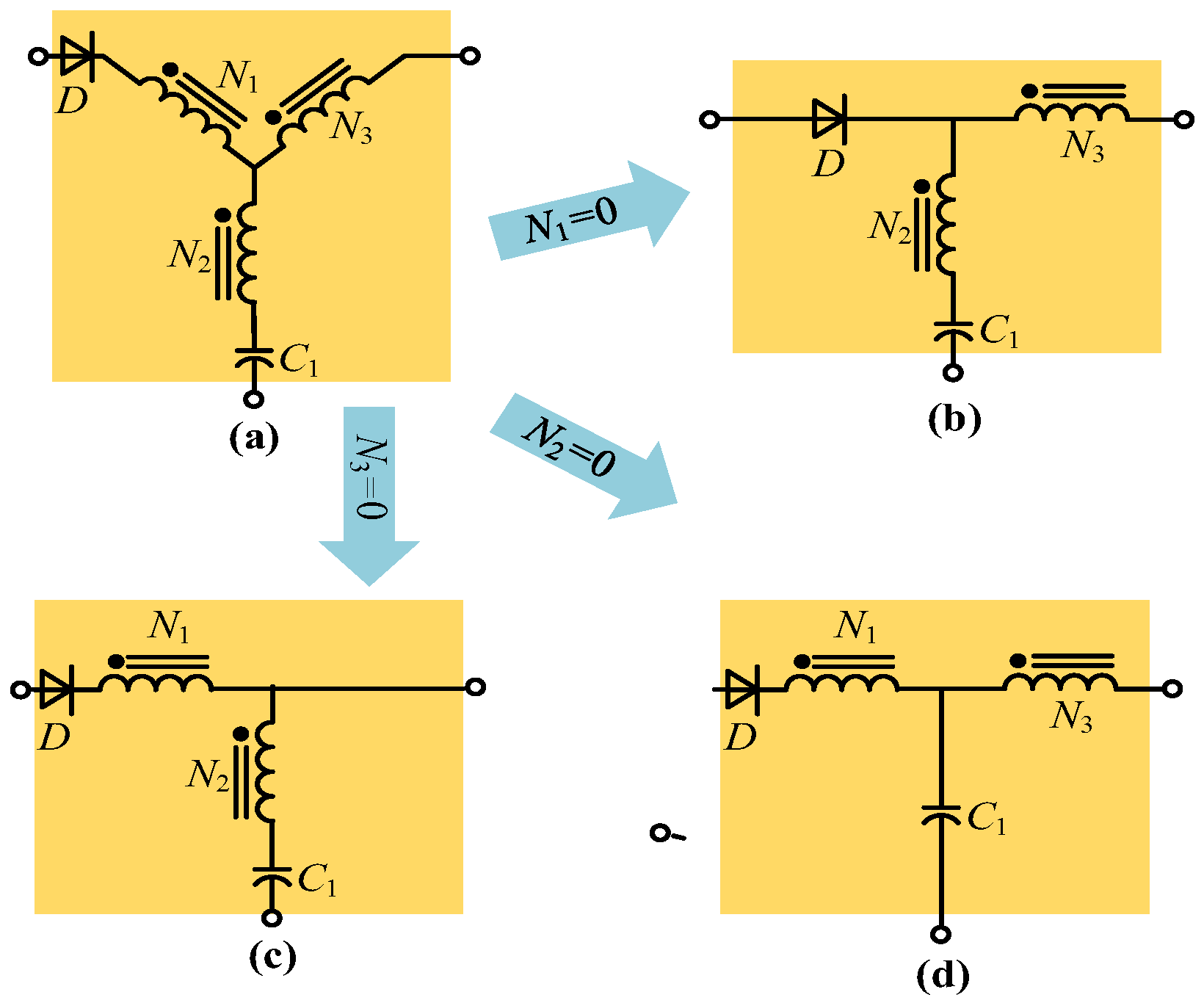
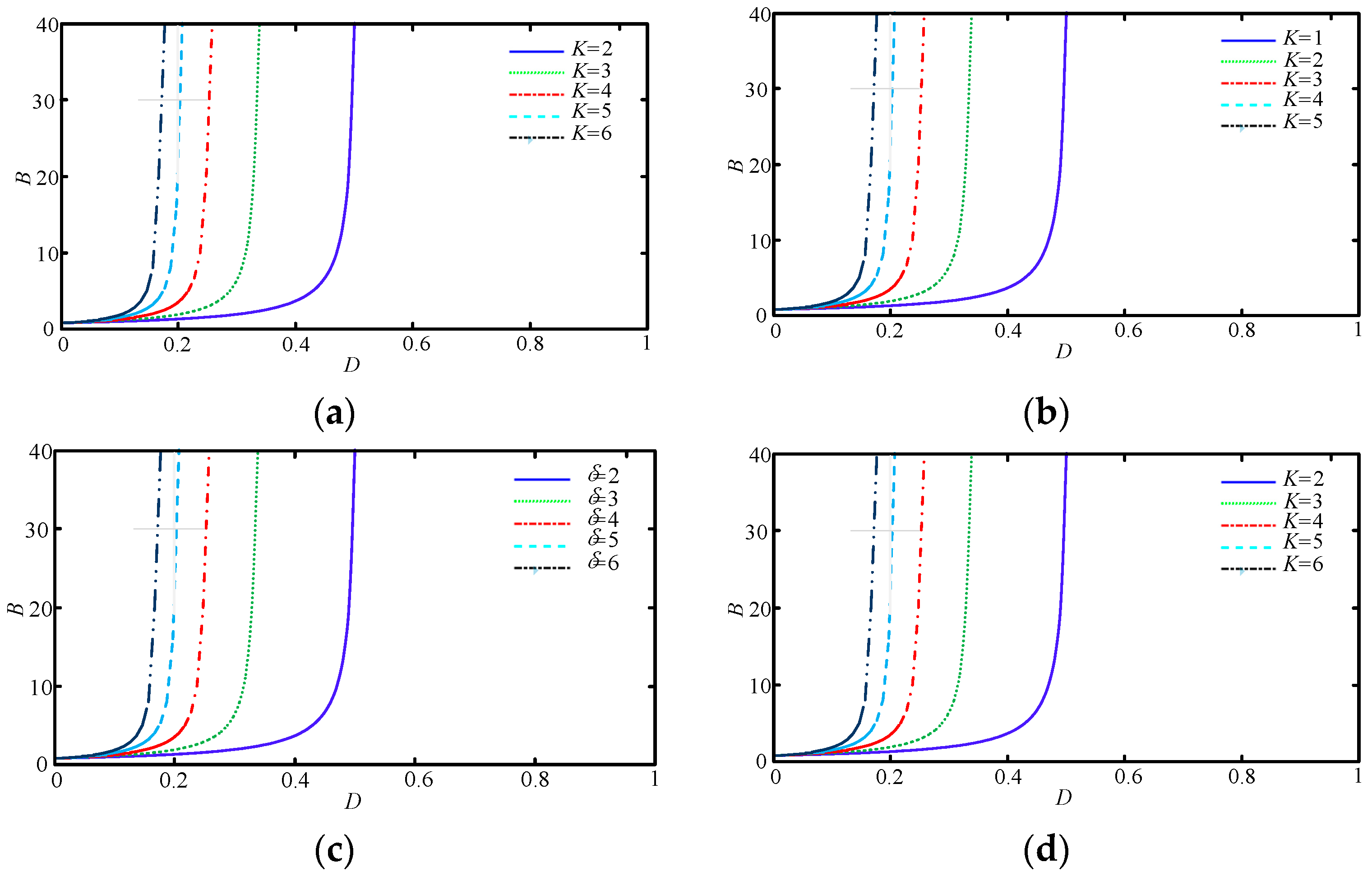
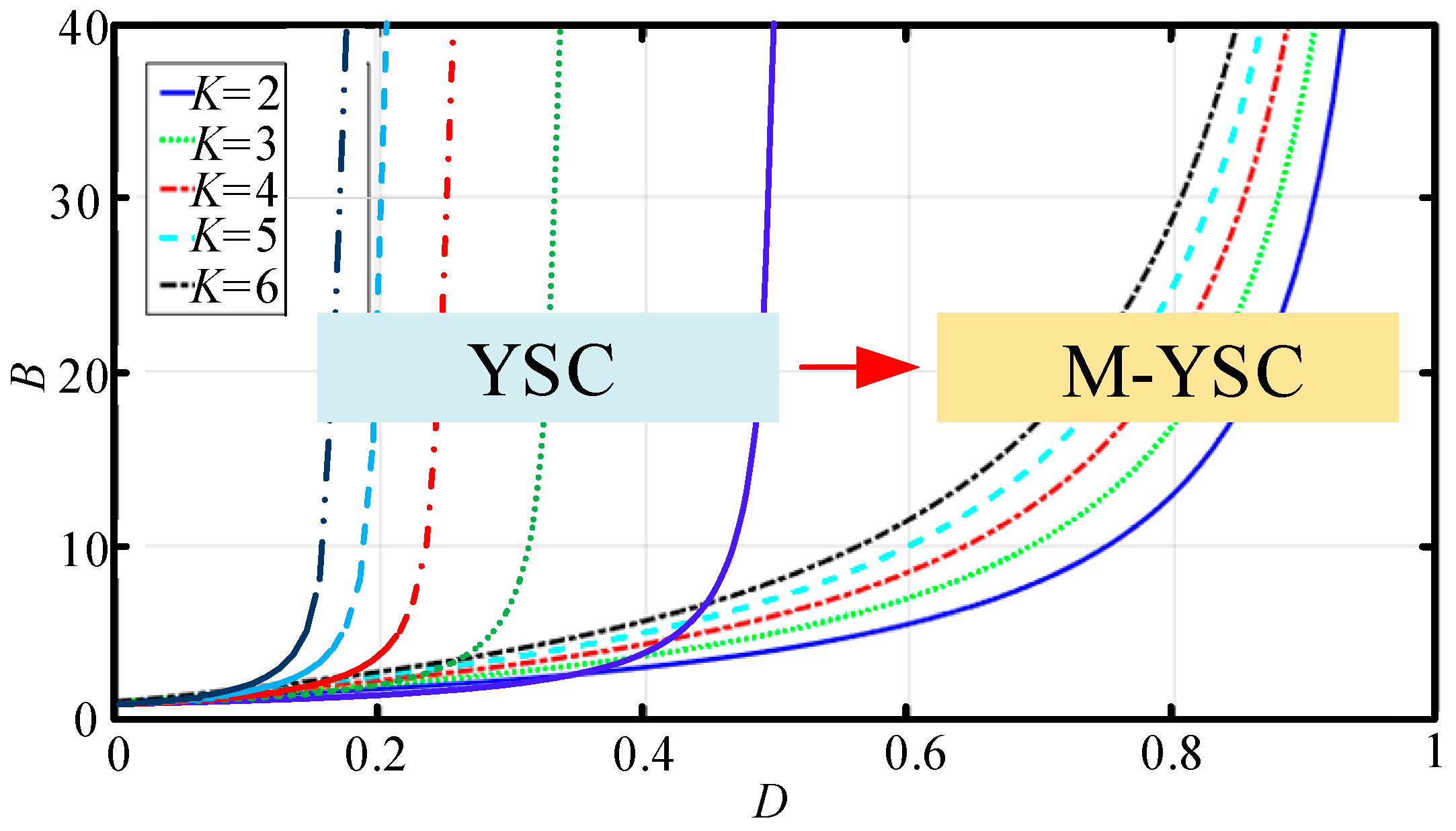
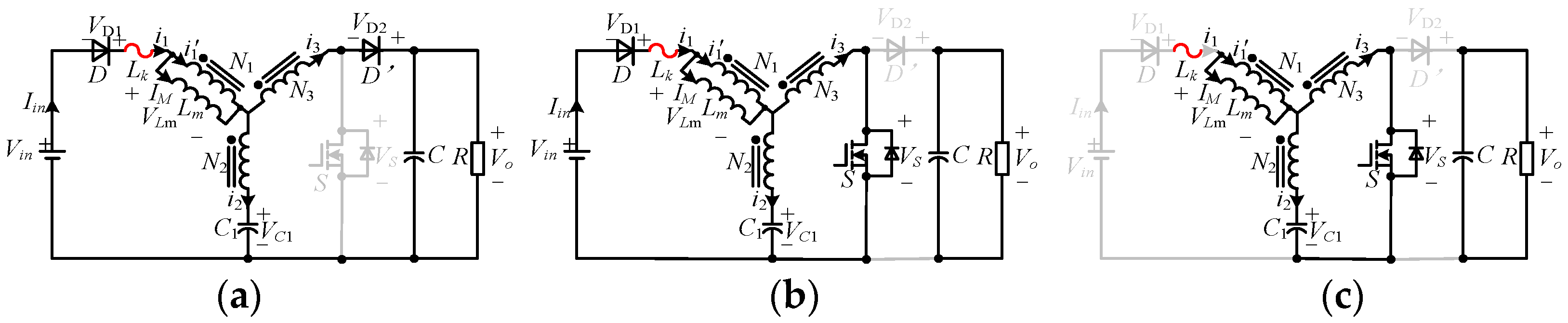
2.1. Traditional Y-Source Converter (YSC)

As shown in Figure 4, YSC consists of two diodes (D1 and D2), two capacitors (C0 and C1), and a three-winding coupled inductor (N1, N2, and N3). The coupled inductors are charged by the capacitor under the Shoot-Through (ST) state and discharge to the load together with the power supply under the Non-Shoot-Through (NST) state. Its step-up ratio is determined by the turns of the coupled inductors and the duty ratio. Due to the introduction of the coupling inductors, fewer components and the flexible turns ratio are allowed in YSCs.
When the switch S is turned on, the converter is in ST state, as shown in Figure 5a, and the magnetization voltage in the ST state vLm_ST is derived as follows:
N 3 N 1 v L m _ S T N 2 N 1 v L m _ S T = V C 1 v L m _ S T = N 1 N 3 N 2 V C 1
where N1, N2, and N3 are the number of turns of the windings, VC1 is the voltage across C1, and VNX is the voltage across NX.
In the NST state, as shown in Figure 5b, according to the KVL, the magnetic voltage in the NST state vLm_NST is derived as follows:
v L m _ N S T + N 2 N 1 v L m _ N S T = V i n V C 1 v L m _ N S T = N 1 N 1 + N 2 ( V i n V C 1 )
v L m _ N S T + N 3 N 1 v L m _ N S T = V i n V o v L m _ N S T = N 1 N 1 + N 3 ( V i n V o )
where Vin is the input voltage, Vo is the output voltage, and vLm_NST is the voltage of Lm in the NST state.
According to the volt-second balance of vLm in one switching period, the equation is as follows:
0 T S v L m = 0 d v L m _ S T + ( 1 d ) v L m _ N S T = 0
Based on the above analysis, the expression for the boost ratio is as follows:
V o = 1 1 K d V i n B = V o V i n = 1 1 K d
K is defined as the winding factor, and its expression is as follows:
K = N 3 + N 1 N 3 N 2 ,
It can be seen from Equation (5) that the boost ratio is determined by the winding factor and the duty ratio. However, the duty ratio has the following restrictions:
1 K d > 0 d < 1 K
The corresponding relationship among the number of turns, winding factor K, duty cycle d, and boost ratio B is shown in Table 1:
It can be seen from Table 1, that although the turn ratio is different, the winding factor K is the same as the first column of Table 1. Therefore, the number of turns of the coupled inductor winding is variable, which has greater design flexibility.
Figure 6 shows the voltage gain of improved YSC with different winding factors. It can be seen that the duty cycle adjustment range of YSC is less than 0.5 when K > 2.
Table 2 shows that the Y-Source has the highest voltage gain and design flexibility among the networks mentioned above. In addition, if n13 and n32 of the YSC are considered as the turn ratio of the T-source and Γ-source, then the voltage gain satisfies the following relationship:
B T Z = ( 1 ( 1 + n 13 ) d ) 1 = ( 1 V T Z d ) 1
B Γ Z = ( 1 ( 1 + 1 n 32 1 ) d ) 1 = ( 1 V Γ Z d ) 1
The expression for VTZ and VΓZ are as follows:
V T Z = ( 1 + n 13 )
V Γ Z = ( 1 + 1 n 32 1 ) .
According to Equations (8)–(11), it can be calculated as follows:
B Y = ( 1 K d ) 1 = ( ( 1 1 + n 13 1 n 23 ) d ) 1 = ( 1 + ( 1 + n 13 ) ( 1 + 1 n 32 1 d ) ) 1 = ( ( 1 + V Y ) d ) 1
V Y = ( 1 + n 13 ) ( 1 + 1 n 32 1 ) = V T Z V Γ Z
According to Equation (13), the gain of the Y-source is a combination of T-source and Γ-source gains. Compared with them, Y-source appears to have a wider application.

2.2. Quasi Y-Source Converters (qYSCs)

Compared with other existing impedance networks, YSC has a higher gain with a small duty ratio and better design flexibility. However, the input current of the YSC is discontinuous, and the inrush current is induced when it starts up.
In response to the issue of discontinuous input current, Figure 7a shows a method to smooth the input current using an additional capacitor. However, the charging process of the capacitors will cause a large start-up pulse current. Moreover, capacitors C1 and C2 need to maintain a particular proportional relationship, and they are prone to resonate with the input side parasitic inductance, which increases the design difficulty.
In Figure 7b, a new method is proposed, which adds an input inductor and a capacitor to solve the discontinuity of the input current [36,37]. It can effectively suppress the pulse current, but high voltage stress for the input diode is inevitable.
On this basis, a new topology was proposed by exchanging the positions of capacitor C2 and diode D1, as shown in Figure 7c [38]. It can achieve continuous input current without increasing the voltage stress on its components. Moreover, a capacitor is placed to block the current flowing through the coupled inductor, which is beneficial for preventing its core from saturation. However, its boost ratio is lower than YSC.
By changing the position of the D1 in Figure 7c, a new topology can be obtained. The Power supply charges capacitor C1 through inductor L1 and diode D1 at startup. It is not until C1 reaches a steady state that the current flows into the coupled inductors. Although this method protects the primary circuit from the impact of the inrush current, the voltage stress of the power components is still high.
Because the curves coincide, the voltage gains of the qYSCs are represented separately, as shown in Figure 8. Both qYSC-I and qYSC-IV maintain the boost ratio of traditional YSC, therefore the voltage gains of the YSC and the qYSC-I, qYSC-IV are the same as YSC, as shown in Figure 8a,d. The winding factor of qYSC-III is defined as δ = (N1 + N2)/(N2N3). By replacing K with δ, the boosting capacity curve of qYSC-III can be obtained, as shown in Figure 8c. In addition, qYSC-II can achieve the same boost ratio as traditional YSC with a smaller K, and its boost capability curve is shown in Figure 8b.

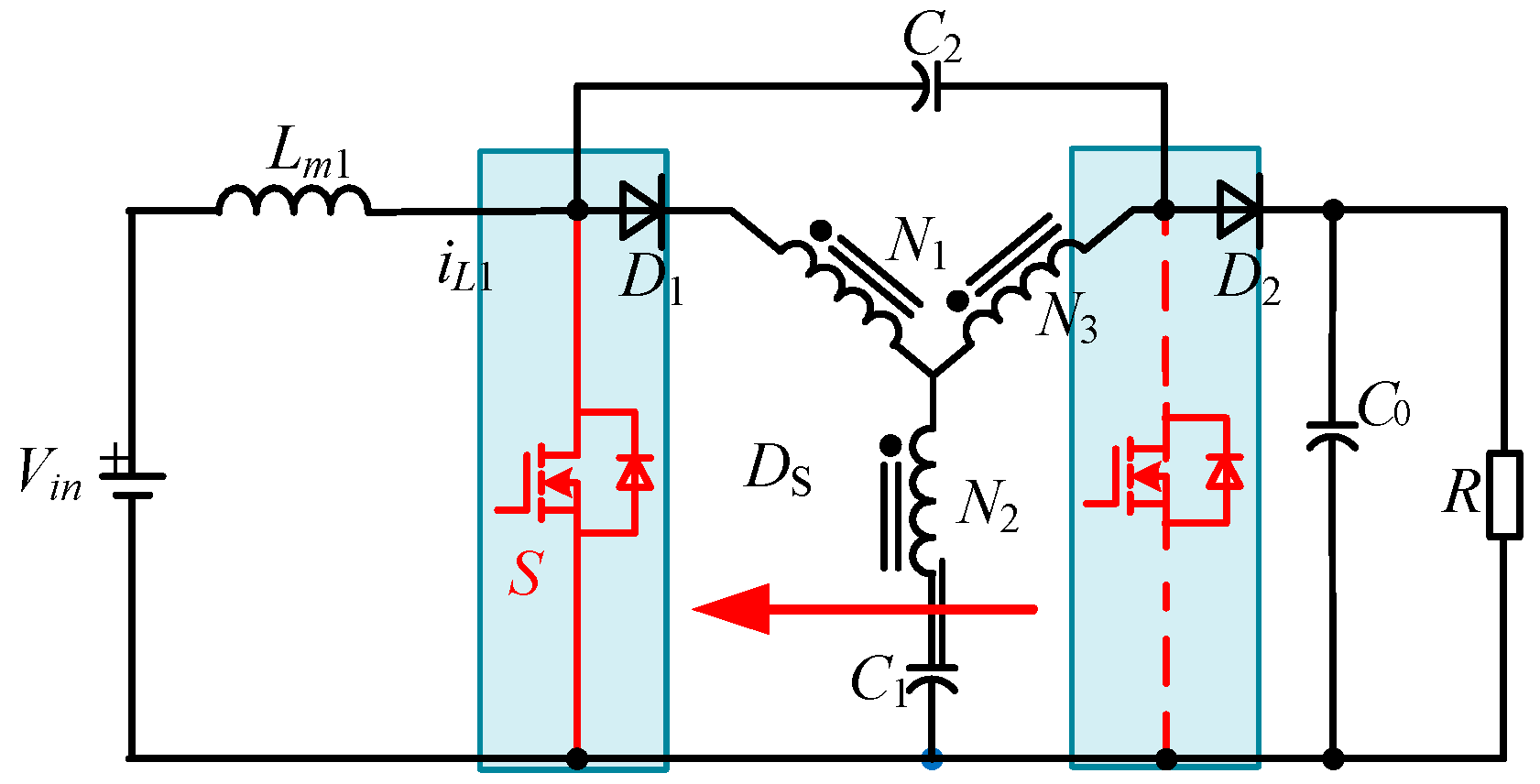
2.3. Modified Y-Source Converter (M-YSC)

To solve the problems of high voltage stress on switches, based on Figure 7b, a Modified Y-source converter was proposed [39]. As shown in Figure 9, the switch is moved from the output side to the input side, avoiding the impact of high voltage on the output side. According to Equation (5), the boost ratio of M-YSC can be obtained.
B = 1 + K d 1 d
According to Equation (14), the corresponding relationship among the number of turns, winding factor K, duty cycle d, and boost ratio B is shown in Table 3:
Table 3 shows that different turn ratios can obtain the same winding factor, indicating that M-YSC has high design flexibility. From Figure 10, it also can be seen that M-YSC has a wide duty cycle adjustment range. Therefore, it can achieve high voltage gain with different winding factors.

2.4. Properties Comparison among Different Impedance Source Networks

Table 4 shows that the voltage stress of the qYSC in Figure 7a is the same as that of the YSC in Figure 4, and its input current is continuous, which is beneficial for the application in new energy generation systems. Under the same voltage gain, the voltage stress on D1 in Figure 7b,d is higher than that in Figure 7a,c. The qYSC in Figure 7c can block input current from flowing through the coupled inductor, but its boost ratio has decreased. Compared with the topology mentioned above, the M-YSC in Figure 9 has the widest duty cycle adjustment range and the lowest switching stress. However, it still has the problem of a large input current ripple, which needs further optimization.
In summary, both the qYSC and M-YSC achieve continuous input current, while their characteristics are different. They provided a foundation for optimizing the Y-source topology, and most of the new structures have evolved from them.

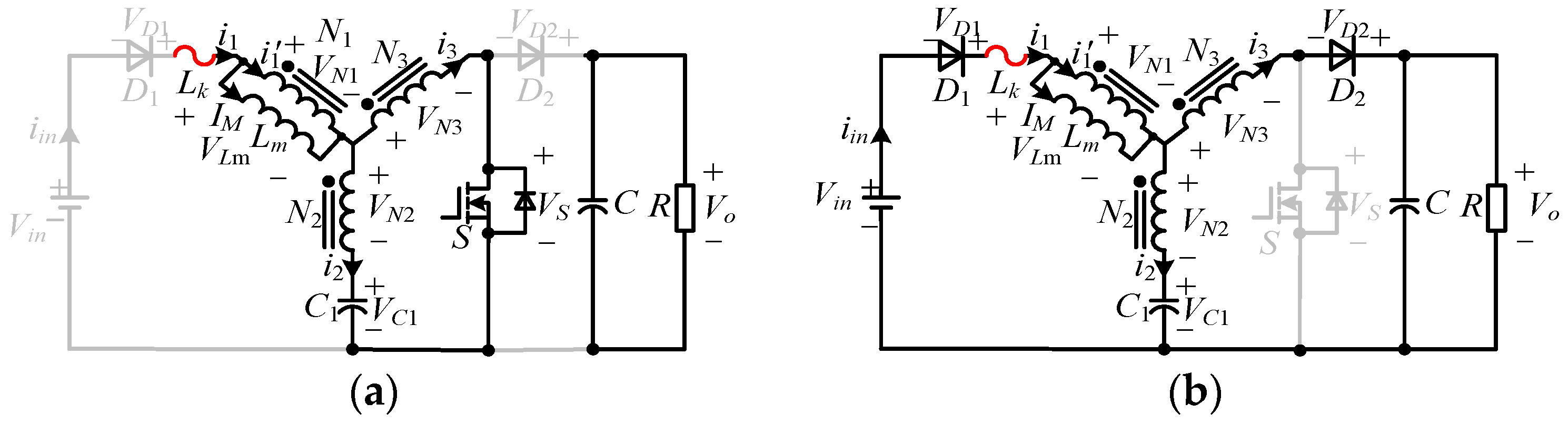
3. Effects of Leakage Inductances on Y-Source Network

3.1. The Analysis of the Effects of Leakage Inductances

The coupled inductors have been used with YSC for high boost capability and design flexibility. However, the above analysis is based on an ideal model without considering the effects of leakage inductance. In response to this issue, the traditional Y-source network is analyzed as an example in [40,41]. When the transition from ST to NST state happens, leakage inductances prevent D1 from immediately turning off, resulting in an intermediate state, as shown in Figure 11b. During this process, its current might increase rapidly in a short time, resulting in a significant voltage overshoot appearing in the circuit, which decreases the utilization of DC voltage and limits the application of YSCs.
The voltage of coupled inductors in different states is shown in Table 5. According to [39], the expression for Δd is as follows:
Δ d = | L N 1 I i n ( N S T ) V L 1 T | | L N 1 P V L 1 V d c ( 1 d ) T |
Due to the presence of intermediate states, the effective duty cycle is shortened to d′ = d − Δd < d. Moreover, the voltages of the inductors Lm satisfy the volt-second balance in one switching cycle. Therefore, the equation is as follows:
d V L ( S T ) + Δ d V L ( I N T ) + ( 1 d Δ d ) V L ( N S T ) = 0
According to Equation (5), the more the duty cycle decreases, the lower the voltage gain. Moreover, when the converter switches from ST to NST state, the influence is related to the types of load. If there is a capacitive load, that can rapidly absorb the changing currents, as shown in Figure 12a, it will not generate voltage overshoot. However, if there is an inductive load, the current through LN3 will be pulled down to the load current value almost instantaneously. At this point, the rapidly changing current, which acts on the leakage inductance, will generate a high voltage overshoot, as shown in Figure 12b. The connection between the converter and the inductive load is shown in Figure 13b, which is unlike the capacitive arrangement shown in Figure 13a. By arranging the load in this way, different behaviors during the transitions between the ST and NST states can be demonstrated.

3.2. The Low-Voltage-Overshoot Y-Source Converters

To solve the problem caused by leakage inductance, scholars have proposed a series of new topologies with voltage-clamp cells. According to their structures and characteristics, they can be divided into the following classes:

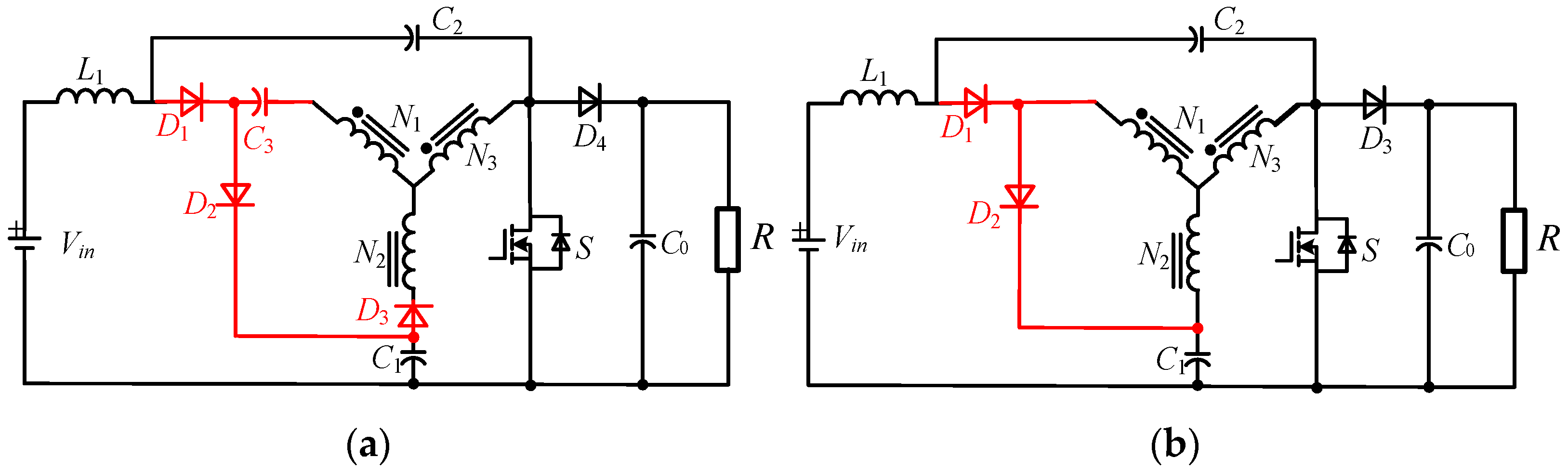
3.2.1. The Voltage-Double Quasi Y-Source Converters (VD-qYSCs)

To eliminate the influence of leakage inductance, diodes D2, and D3 are added to the qYSC in Figure 14a. In the intermediate state, D1, D2, C1, and C2 form the clamped circuit, which limits the voltage overshoot. However, in the circuit formed by D2, D3, and coupled inductor, there is a significant voltage drop at the dc-link in comparison to the NST state, resulting in a sharp increase in the circuit current. To simplify the topology, As shown in Figure 14b, the capacitance C2 and diode D3 are reduced, while the boost ratio of the new topology has been decreased [42,43].

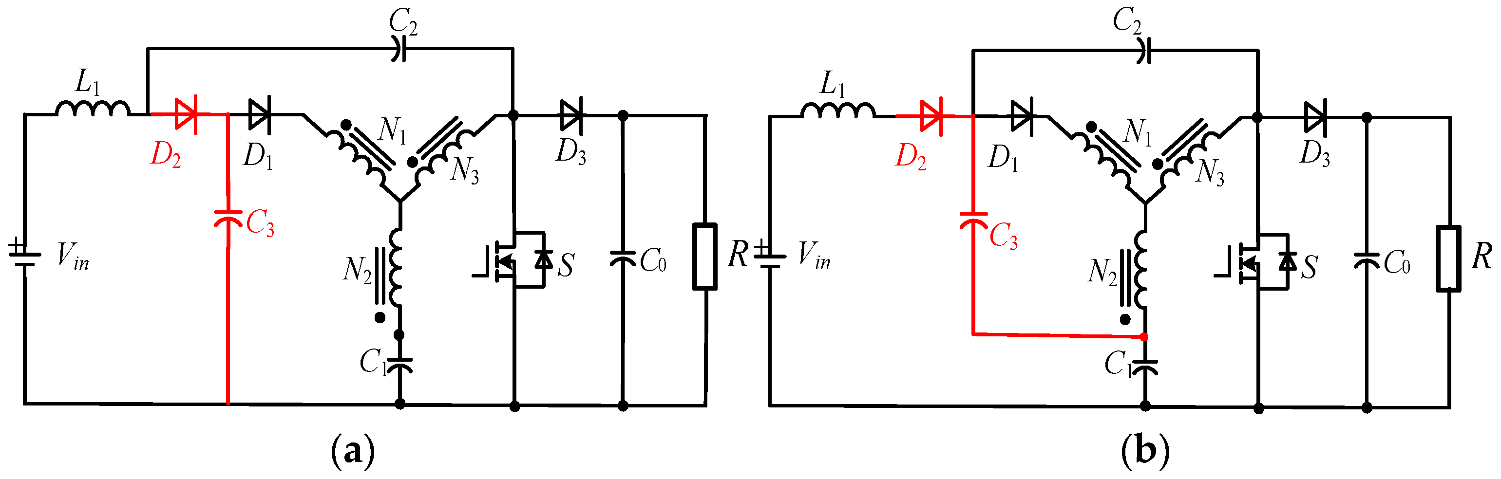
3.2.2. The Low-Voltage-Overshoot High-Efficiency Quasi Y-Source Converters (LH-qYSCs)

To reduce the voltage stress of the power device, a family of low-voltage-overshoot and high-efficiency converters (LH-qYSC) [44] is proposed. A clamped circuit is formed by adding a diode D2 and a capacitor C3, which can absorb the leakage inductance energy and improve the efficiency of the YSC. Figure 15 shows six topological structures. Among them, LH-YSC-I, II, and III are only different in the connection of capacitor C3, while LH-qYSC-IV, V, and VI have been modified from LH-qYSI-I, II, and III. These topologies can effectively clamp the bus voltage, with only different voltage and current stress across the capacitors.

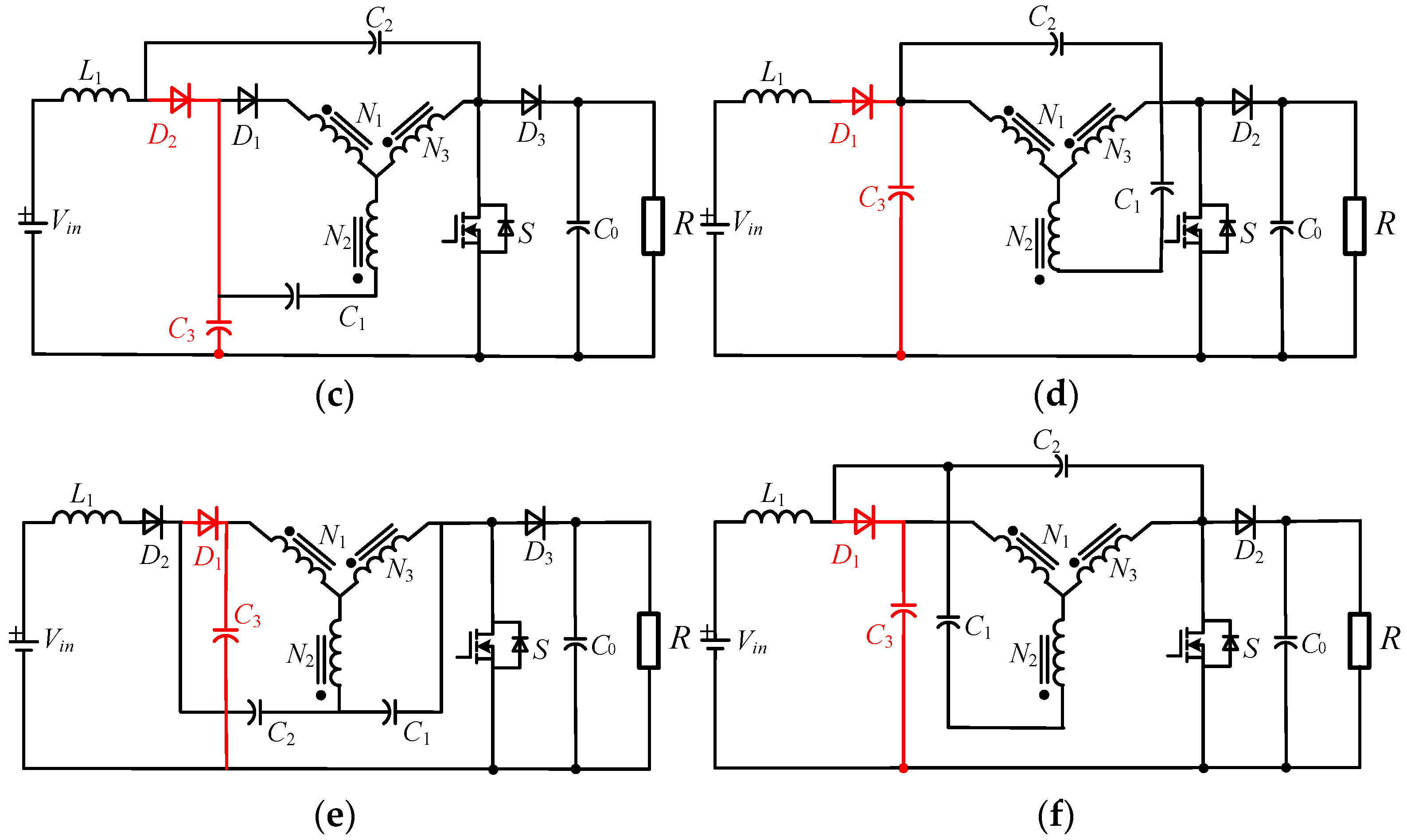
3.2.3. The Low-Voltage-Overshoot High-Step-Up Quasi Y-Source Converters (HS-qYSCs) and the Diode-Assisted Quasi Y-Source Converter (DA-qYSC)

To further improve the boost ratio of the converter, an inductor, and a capacitor were added to the clamped circuit of the LH-YSC, forming a family of low-voltage-overshoot High-Step-up Y-Source Converters (HS-qYSC). However, they are different in the selections of the basic topology, which leads to differences in their characteristics. Moreover, the position of the absorbing circuits relative to the basic topology is different, resulting in a difference in the voltage and current stress. Specifically, if capacitor C4 in Figure 16c is replaced with a diode, a Diode-Assisted quasi Y-Source Converter (DA-qYSC) can be obtained. As shown in Figure 17, the absorbing circuits of it are identical to that of HS-YSC, so it is not discussed in detail here [45,46].

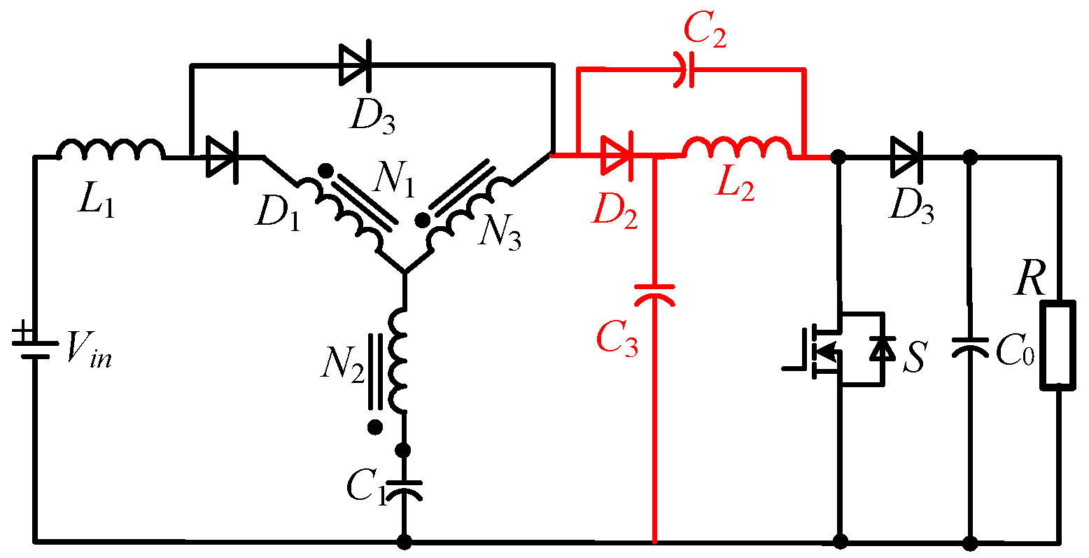
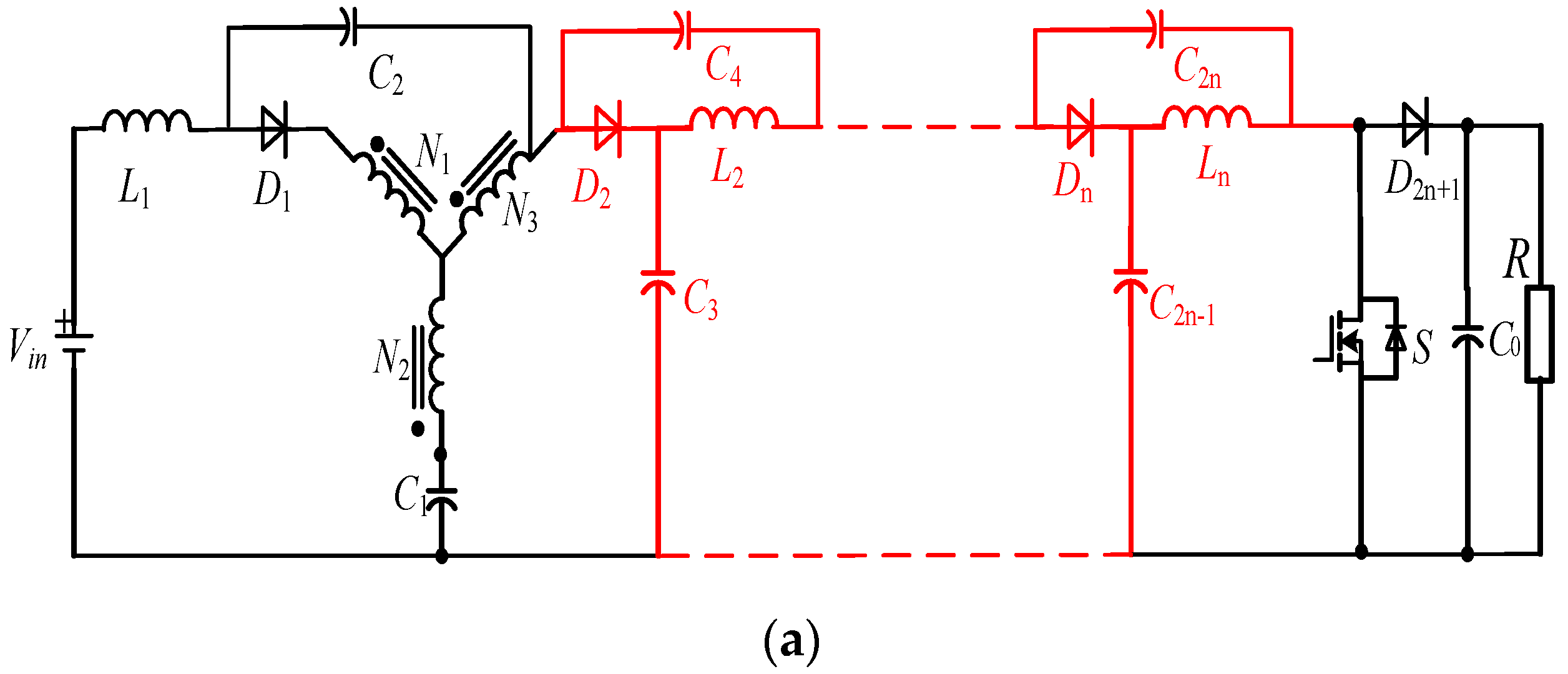
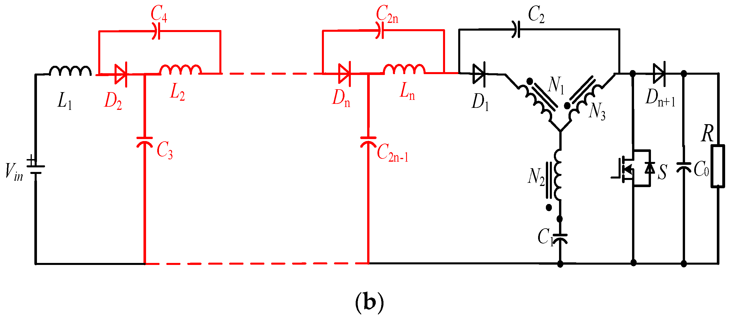
3.2.4. The Low- Voltage-Overshoot High-Step-Up Cascaded Quasi Y-Source Converters (HSC-qYSCs)

As shown in Figure 18, by cascading the absorbing circuits of the HS-YSC, two Low-voltage-overshoot High-Step-up Cascaded quasi Y-Source Converters (HSC-qYSC) can be obtained. When Dn is on, C2n and C2n−1 are in series across the dc-link, which clamps the bus voltage. Moreover, the two topologies have a common gain, which can be expressed as
B = 1 1 ( 1 + n + K ) d

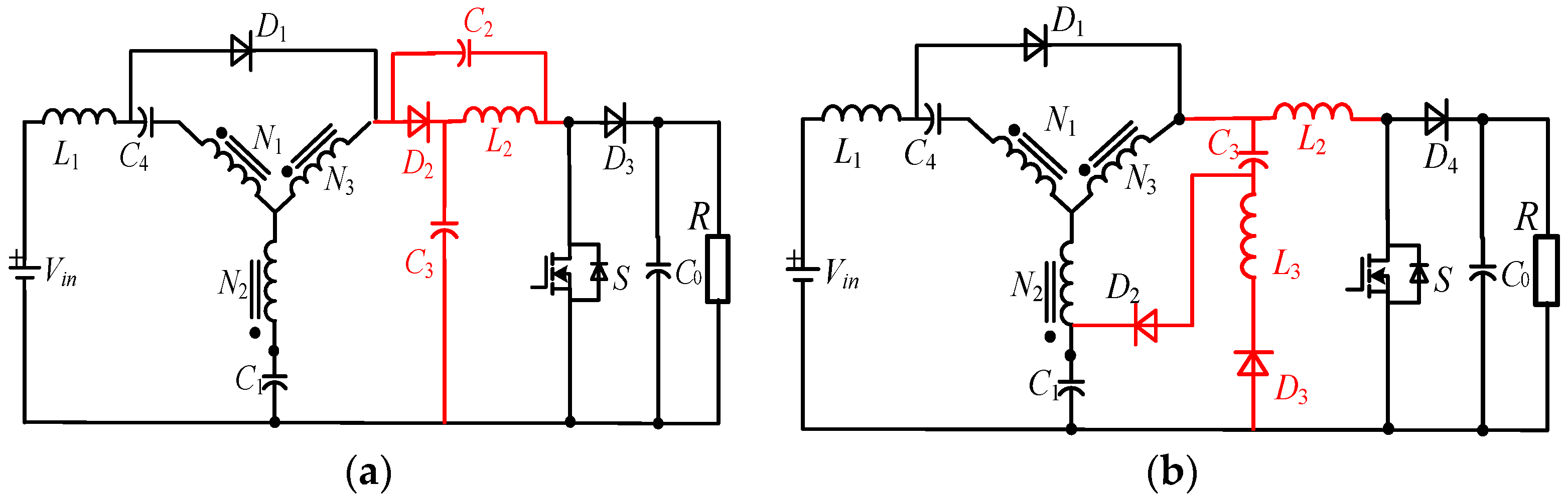
3.2.5. The Optimized Quasi Y-Source Converter (O-qYSC) and the Inductor-Capacitor-Diode Quasi Y-Source Converter (LCD-qYSC)

Although the above topologies have a significant effect in terms of clamping voltage overshoot, they ignore the volume of the coupled inductor. In the YSC, the minimum value of the DC magnetizing current equals the input current. Due to the high input current, the DC magnetization current is large. Therefore, a large volume of the coupled inductors is required to prevent magnetic core saturation. By adding the same absorbing circuits as HS-qYSC (or DA-qYSC) to the qYSC shown in Figure 7c, an Optimized Y-Source Converter (O-qYSC) is proposed in Figure 19a [47]. Due to the zero average magnetizing current, the windings’ current is low, reducing the volume of the coupled inductor significantly. Therefore, it is conducive to achieving higher power density. Similarly, instead of cascade technology by an Inductor-Capacitor-Diode (LCD) buffer, as shown in Figure 19b, an Inductor-Capacitor-Diode Y-Source Converter (LCD-qYSC) is proposed. It can absorb the energy of the leakage inductance without damage, but the component stress of LCD is related to the value of the leakage inductance, leading to difficulty in design [48].

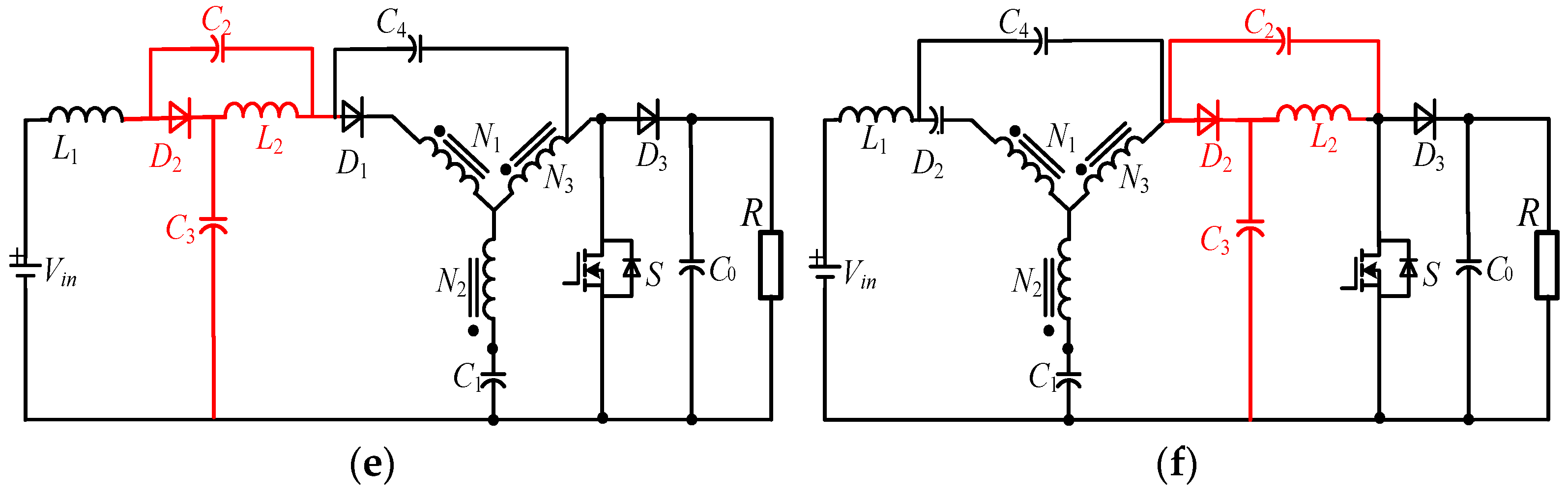
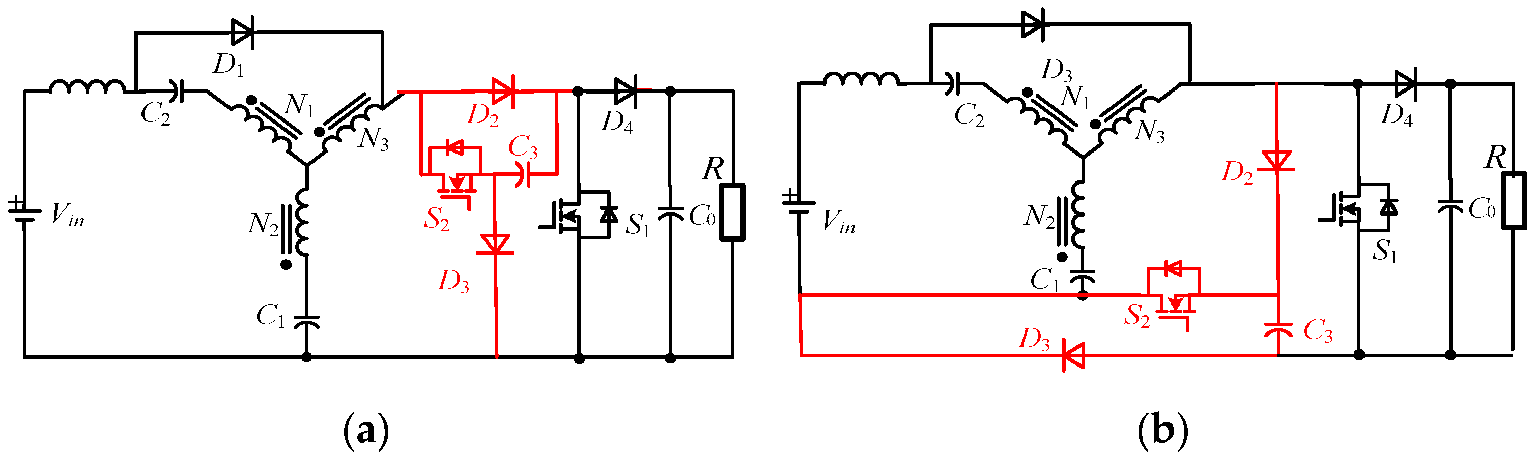
3.2.6. The Active Clamped Quasi Y-Source Converters (AC-qYSCs)

In addition to the impact of voltage overshoot, the value of the ST current cannot be ignored. In the ST state, the current flowing through the circuit is proportional to the ST current. The direct current increases with the decrease of the duty cycle, increasing device stress and circuit loss [49]. To address this issue, one more winding is integrated into the input inductor magnetic core of the quasi-switched boost inverter. However, the switch experiences high voltage overshoot and the input current deteriorates. By replacing the discrete inductor with a switch-coupled inductor, a new topology structure is proposed in [50]. But it still has voltage overshoot on the DC bus. Besides, the magnetizing current of these converters is always larger than the input current, and a large coupled inductor is required.
For this reason, the AC-qYSCs are proposed in [51], which add only two diodes, a switch, and a capacitor compared to qYSC. As shown in Figure 20, these converters use D2, D3, and C3 to form an absorbing circuit of the leakage inductance and clamp the bus voltage by C3, and the volume of coupled inductors is reduced. However, due to the increasing number of switches, the control strategy of the AC-qYSCs becomes complex.

3.3. Properties Comparison among Different Y-Source Converters with the Absorbing Circuit

As can be seen from Table 6 and Table 7, the O-qYSC, and AC-qYSC have high boosting ability, while the DA-qYSC, and O-qYSC have lower voltage and current stresses. Regarding the effect of the DC magnetization current, the coupled inductors of the O-qYSC, LCD-qYSC, and AC-qYSC can be designed to be smaller, which is beneficial for obtaining higher power density. Moreover, only the AC-qYSC suppresses the ST current to 0.5δIin, while it is δIin for others. It indicates that with the same ST current, the value of δ of the AC-qYSC can be doubled, which provides greater design flexibility. Nevertheless, when δ is large, the ST current and voltage stress of the AC-qYSC are relatively high. Therefore, the value of δ should be appropriate.

4. The Optimization of YSCs’ Key Indicators

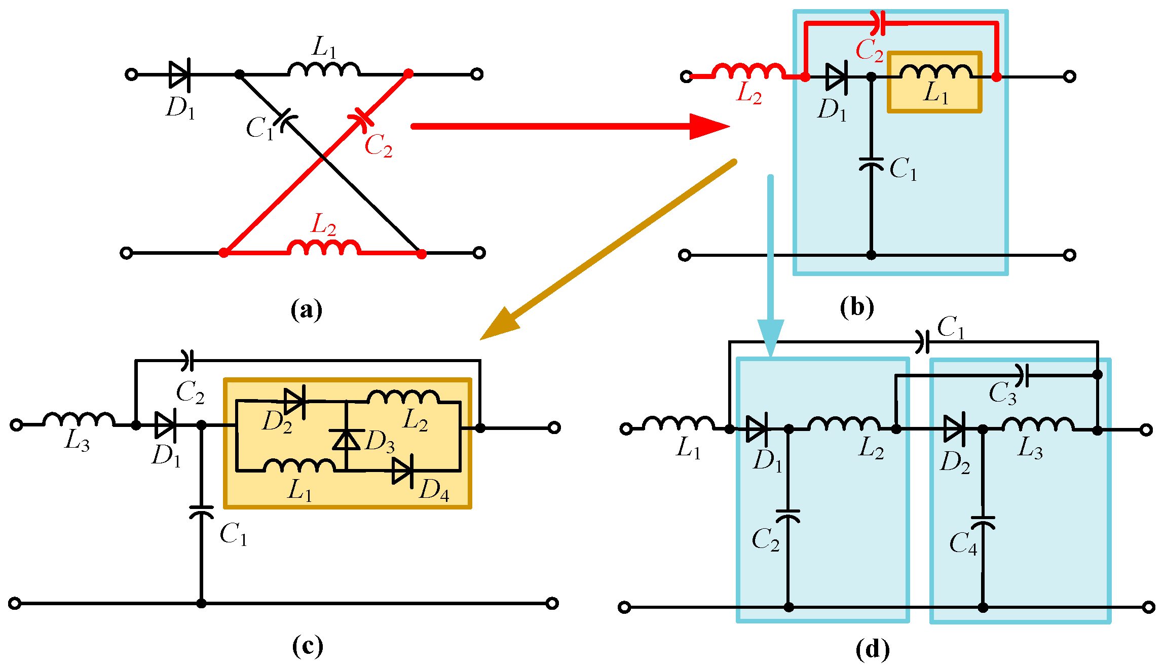
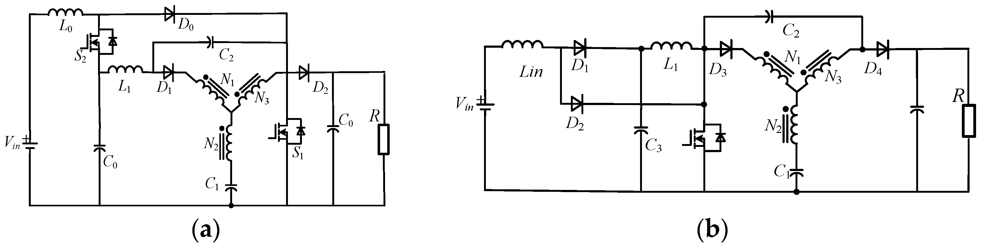
4.1. The Y-Source Converters Combined with Various Boosting Structures

To further improve the gain, various boosting structures are combined with the Y-source converter. The main topology structure is as follows:

4.1.1. The Y-Source Converters Combined with a Boost Converter

  • The Quasi Y-Source Converters combined with a Boost Converter (CB-qYSC)
By combining the qYSC with a boost converter, an improved quasi-Y-source converter was proposed in [52], as shown in Figure 21a, which inherits all the advantages of qYSC. Moreover, a high boost radio can be realized by controlling two switches of S1 and S2. Nevertheless, two switches increase the converter cost, and the design of the control strategy becomes more difficult.
2.
The Modified Y-Source Converters combined with a Boost Converter (CB-M-YSC)
Based on the M-YSC, a single-switch Y-source converter is proposed in [33], as shown in Figure 21b. Due to the active switch being shared between the M-YSC and the traditional boost converter, the design of the control strategy is simpler than that of the CB-qYSC. In addition, all advantages of the M-YSC, high voltage boost, and low voltage stress, are inherited. However, the adjustment of the boost ratio is more dependent on the duty cycle, and the effect of the winding factor is weakened. Therefore, it is considered to combine the y source with different boost units to further improve the voltage gain.

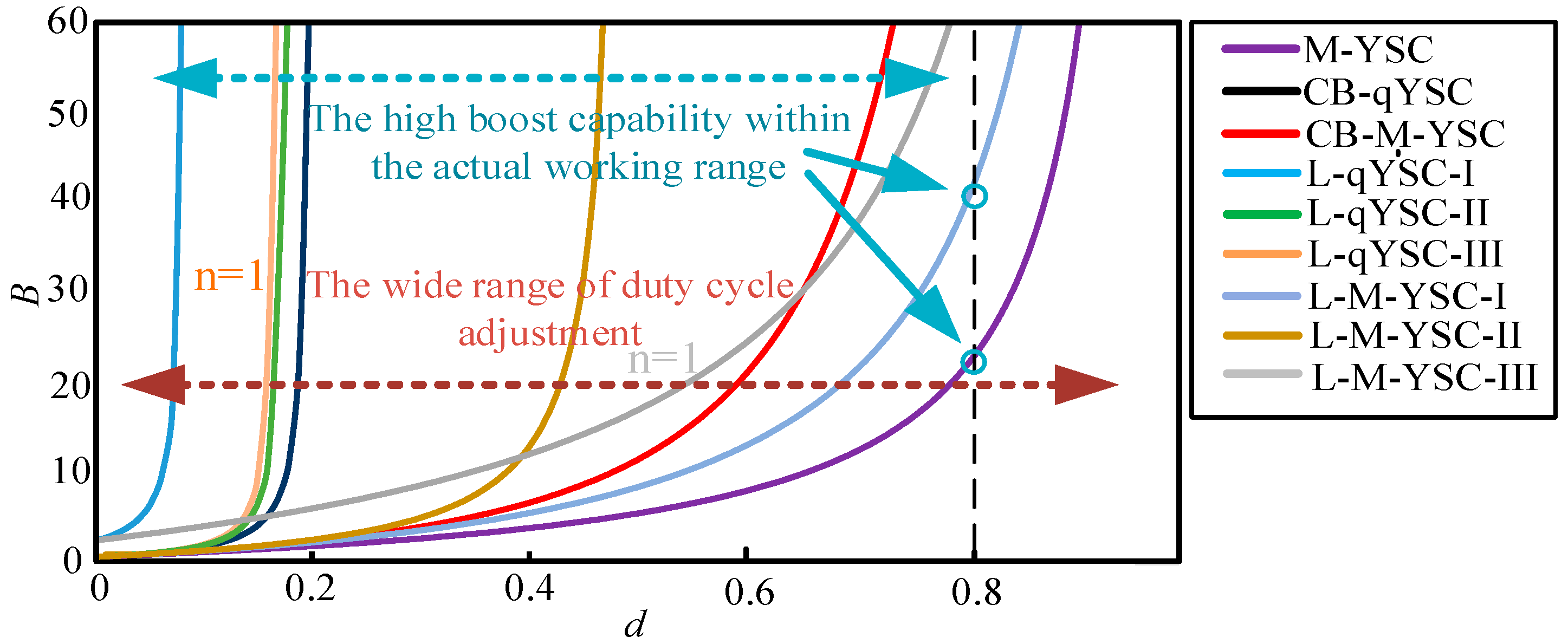
4.1.2. YSC Combined with Different Step-Up Cells

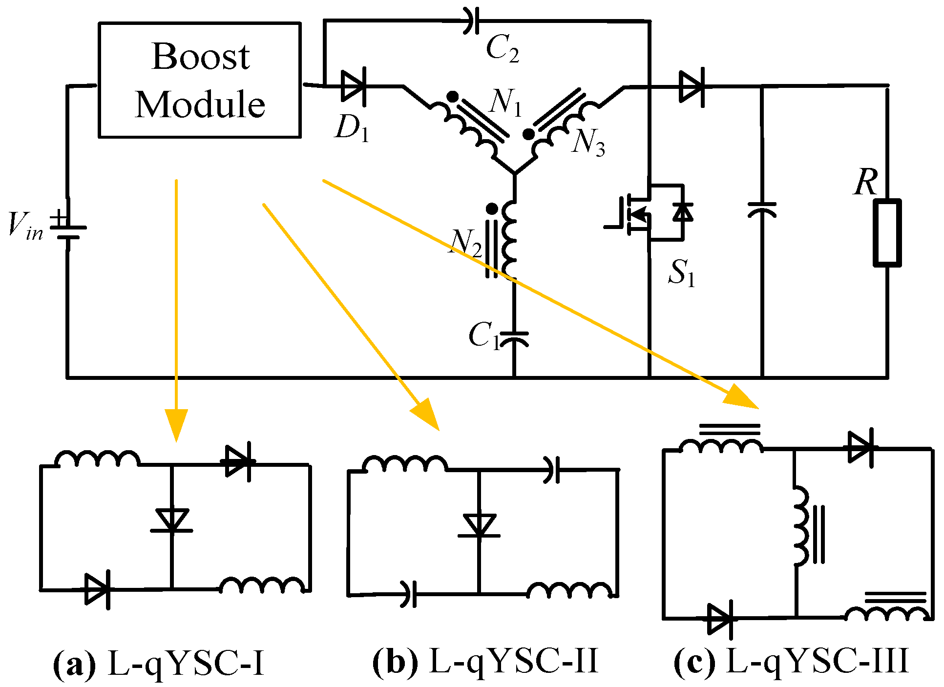
  • The quasi Y-Source Converter with series Inductance modules (L-qYSC)
To further improve the boost ratio of the converter, a family of new High-Step-up Y-source converters was proposed in [53], which combined the qYSC with different step-up cells, including switch inductors (SL) [54,55,56,57], Quasi-Z-source networks (QZ) [58], and Switch-Coupled Inductors (SCL). After being connected with qYSC, SL-Y-Sources Converter (L-qYSC-I), QZ-Y-sources converter (L-qYSC-II), and SCL-Y-sources converter (L-qYSC-III) are sequentially obtained, as shown in Figure 22. Although the step-up cells provided continuous input current and higher voltage gain than qYSC, the disadvantages of qYSC, such as the high voltage stress of the switch and the narrow duty cycle control range, are inherited.
2.
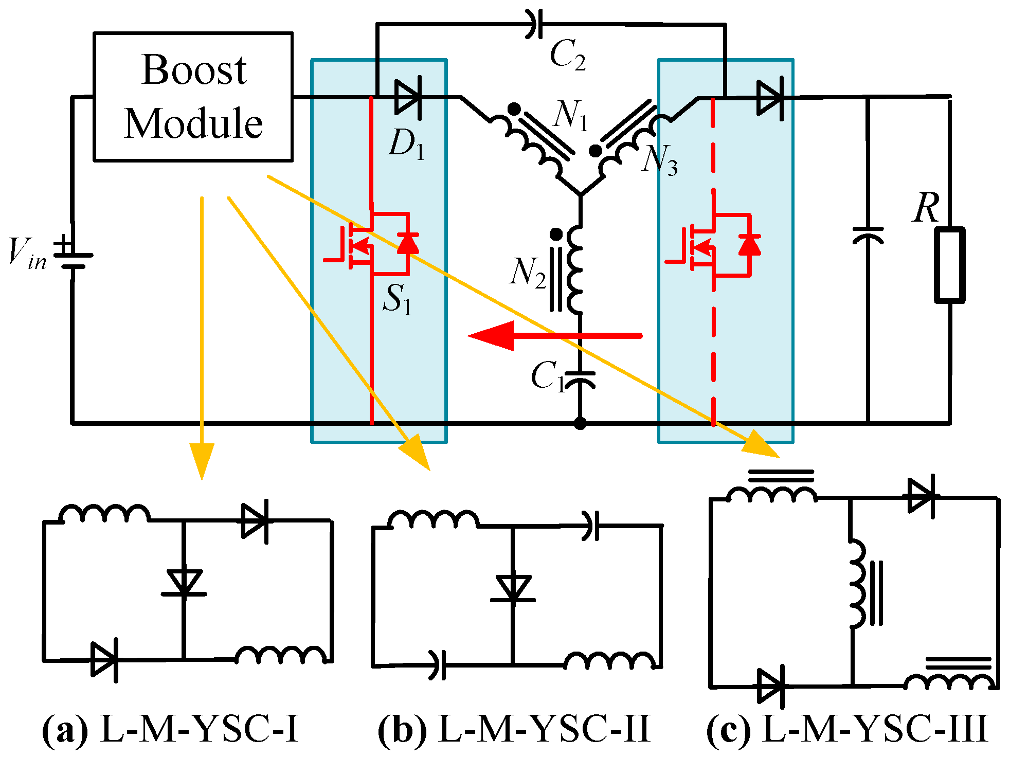
The Modified Y-Source Converter with Series Inductance Modules (L-M-YSC)
On this basis, the step-up cells mentioned above were combined with M-YSC to form a series of new topologies, which are shown in Figure 23 [59]. Compared with Figure 22, They further reduced the switch voltage stress, as shown in Table 8. Nevertheless, complex components increase the cost of converters, and further consideration needs to be given to improving their power density.
In addition, if the allowable adjustment range of duty cycle is small, the boost ratio will change significantly with the change of the duty cycle, and a small duty cycle disturbance will have a great impact on the output voltage, making the control more difficult. In addition, if the change of boost ratio with the duty cycle is too small, considering that the duty cycle of the converter is usually less than 0.8 in actual operation, the ideal boost ratio cannot be achieved in actual operation. Therefore, the ideal condition is that the allowable adjustment range of the converter duty cycle is as wide as possible, and the ideal boost ratio can be achieved in the range where the duty cycle does not exceed 0.8. As shown in Figure 24, the relationship between the duty cycle and boost ratio of L-M-YSC-III is the most suitable.

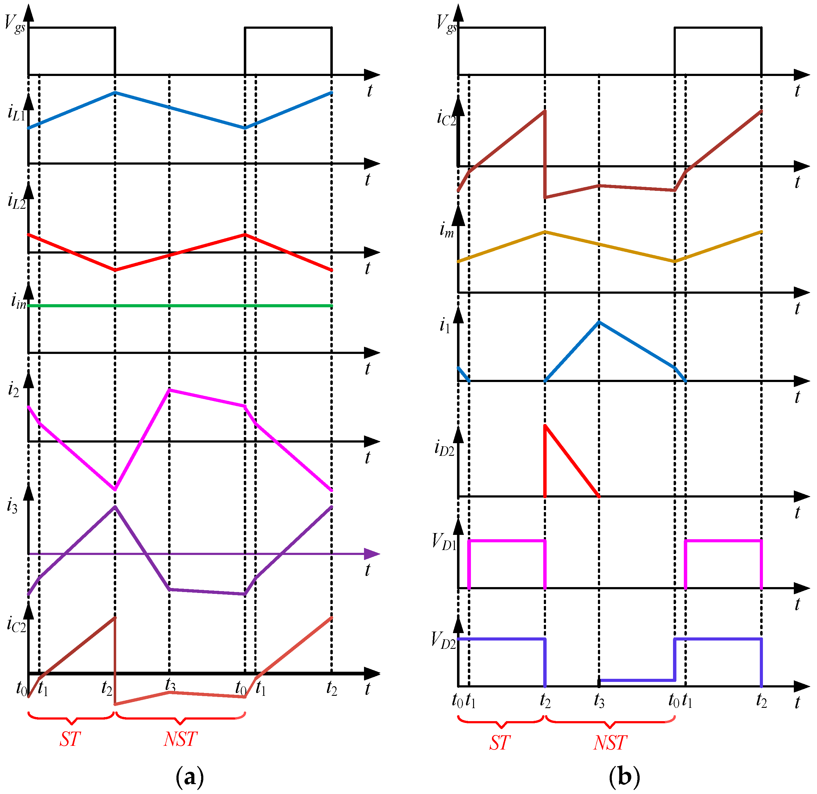
4.2. YSC with Low Input Current Ripple

Although M-YSC has achieved continuous input current, it still has the disadvantage of the large input current ripple. When used in photovoltaic power generation systems, it will reduce the life of the photovoltaic arrays. Therefore, it is necessary to reduce the ripple of the input current [60,61].
There are quite a few approaches to reducing the current ripple. The primary method is to use passive L, LC, or LCL filters, but larger filter inductance and capacitance will increase the volume and cost of the Y-source converters [62]. To reduce the volume of the components, an interleaved paralleled converter is proposed in [63]. However, it has complex control methods, and the input current ripple cannot be completely filtered out. Increasing the switching frequency is also an effective method, which can reduce the current ripple without increasing the application of components. Nevertheless, a large switching loss will be caused. Therefore, a new Y-source converter with low input current ripple and higher performance is required.

4.2.1. A Family of Modified Y-Source Converter with Zero Input Current Ripple (ZICR-M-YSC)

To reduce the ripple of the input current, A family of Modified Y-Source Converters with Zero Input Current Ripple (ZICR-M-YSC) is proposed in [64]. As shown in Figure 25a, it is based on the qYSC, while Figure 25b is based on the M-YSC. Compared to the qYSC or M-YSC, only one capacitor and two windings are added. Moreover, the advantages of M-YSC, such as the high boost ratio and low voltage stress on switches, are inherited by ZICR-M-YSC.
Figure 26 shows the theoretical waveform of ZICR-M-YSC, and the simulation results are shown in Figure 27. It can be seen that the current ripples of the inductors L1 and L2 cancel each other out so that the input current ripple can be reduced to close to zero.

4.2.2. A Modified Y-Source Converter Using the Conventional Coupled Inductor Filter (CIF-M-YSC)

Figure 28 proposes a modified Y-source converter using a conventional coupled inductor filter [65]. Compared to ZICR-M-YSC, an additional magnetic core is required.
When the switch S turns on, the current of the inductor L1 in the ZICR-M-YSC and the CIF-M-YSC can be expressed as follows:
i 1 ( t 0 ) = N 1 N 1 + N 3 i m ( t 0 ) + N 3 N 2 N 1 + N 3 ( I i n ( n + 1 ) Δ i L 1 2 )
i 1 , C I F ( t 0 ) = N 1 N 1 + N 3 i m , C I F ( t 0 ) + N 3 N 2 N 1 + N 3 ( I i n 1 1 n Δ i L 1 2 )
According to the expression, when n = n′, the current of the CIF-M-YSC is less than that of the ZICR-M-YSC. Therefore, the CIF-M-YSC is more likely to operate in DCM, leading to the current stress of the components increasing, which may reduce the lifespan of the components.
The typical topologies with low input current ripple are compared in Table 9, which shows that YSC and ZICR-M-YSC [63] have fewer components, while YSC has a larger input current ripple. Compared with them, ZICR-M-YSC and the topologies in [64] can achieve zero input current ripple when D > 0.2, and the voltage gain of ZICR-M-YSC is higher than the topologies in [63,64,65,66]. However, the efficiency of the ZICR-M-YSC is lower than M-YSC. Therefore, it is necessary to reduce the losses of the converter.

4.3. High-Efficiency Y-Source Converters

With the widespread application of renewable energy, the requirements for efficiency are higher. However, the switches of all the topologies mentioned above work in a hard-switching state, which leads to large switching loss. Therefore, it is necessary to achieve soft switching, which can reduce the loss of the converter.

4.3.1. The Isolation Type Zero Current Switching Quasi Y-Source Converter (I-ZCS-qYSC)

As is shown in Figure 29, an Isolation type Zero Current Switching quasi Y-Source Converter (I-ZCS-qYSC) is proposed in [68]. By utilizing the parasitic capacitance and leakage inductance of the transformer, Zero Current Switching (ZCS) of all SX and DX is achieved. However, with the introduction of redundant components, the power density of the converter is significantly reduced.

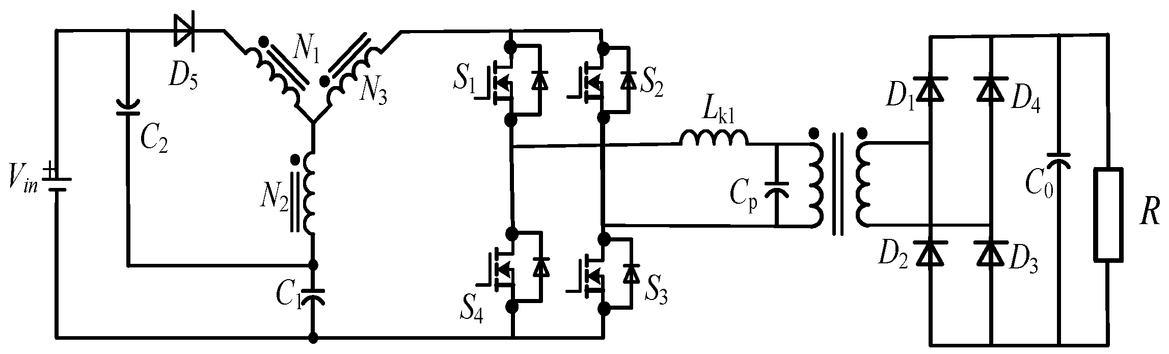
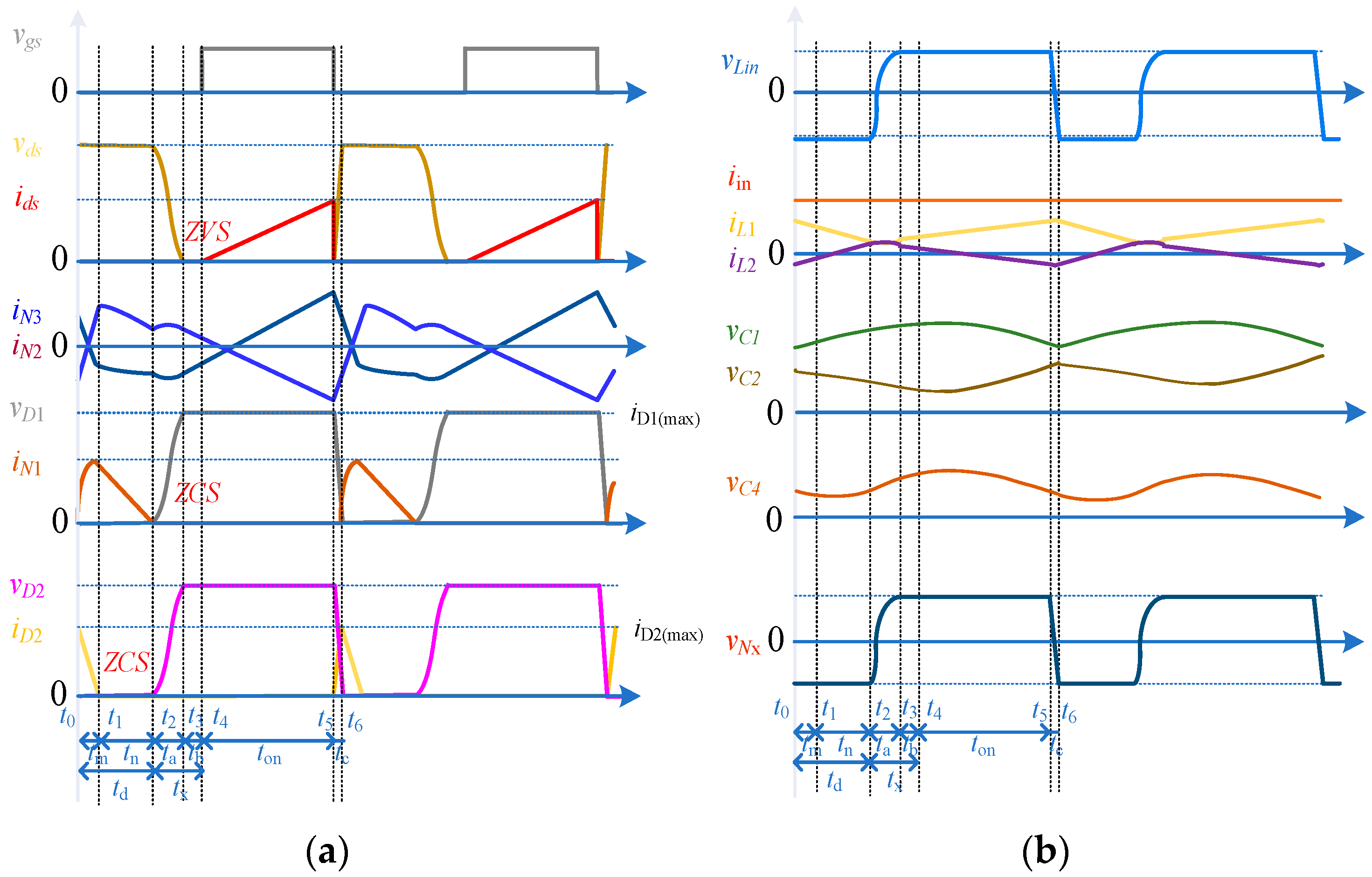
4.3.2. The Modified Y-Source Converter with Soft Switching Characteristic and High Voltage Gain (SH-M-YSC)

As is shown in Figure 30, a Modified Y-Source Converter with Soft switching characteristics and High voltage gain( SH-M-YSC) is proposed in [69], which has fewer components than I-ZCS-M-YSC. Its resonant cell, composed of the capacitor CQ, C1, C2, and the winding N2, N3, operates in the DCM so that all the switches and diodes of the SH-M-YSC work in ZVS and ZCS.
Figure 31 shows the theoretical waveform of SH-M-YSC, while the simulation results are shown in Figure 32 and Figure 33. It can be seen that both the diodes and switch can work in ZCS and ZVS, which is beneficial for improving the efficiency of the system.
As the switch works in ZCS and ZVS, the switching loss is greatly reduced. Moreover, it is feasible to obtain high-boost radio in DCM. When Considering the maximum resonance time, the expression of voltage gain in DCM is given in [69]:
G = 1 + 1 + 2 D 2 T τ 2
According to Equation (20), it can be seen that the voltage gain of the converter is determined by the duty cycle, operating frequency, and the time constant. As the inductance of the coupled inductors decreases, the circuit enters DCM mode, and the output voltage increases with the load, leading to higher voltage gain. Therefore, if the time constant is appropriately selected, soft switching and higher voltage gain can be achieved simultaneously.
In addition, the properties comparison among the converters in [39,64,69] is shown in Table 10, and the efficiency curves of the converters are compared in the same power range in Figure 34. The results show that the SH-M-YSC, which has a simple structure and soft switching characteristic, has higher efficiency when the output power is higher than 150 W. However, under the light load condition, the efficiency of the system is dropped by 2% for the magnetic core loss under higher frequency operation conditions. Therefore, further consideration should be given to achieving high efficiency under light load, which will further improve the performance of YSCs.

5. Conclusions

Due to the advantage of high boost radio and design flexibility, the Y-source network has received widespread attention. In this paper, the derivation of the Y-source converter is summarized, and the characteristics of similar topologies are compared and analyzed. The main conclusions can be summarized as follows:
  • To reveal the corresponding relationship between topology and function, a YSC topology can be divided into basic structure and characteristic circuits. The basic structure (YSC, qYSC, M-YSC) determines the general properties of topology, as shown in Table 2. The clamping circuits, absorption circuits, boost circuit, filtering circuits and resonant circuit in Section 3 and Section 4 are characteristic circuits, which determine the additional functions of the topology. According to the application scenario, the basic structure and characteristic circuits can be selected relatively independently, and the most appropriate topology can be obtained.
  • To solve the problem of voltage overshoot caused by leakage inductance, an additional voltage clamp circuit is added to the basic topology. Changing the position of components will result in different stresses of components, with the clamping principle unchanged. Similarly, the position of boost circuit and absorption circuit is also flexible, which is conducive to improving the comprehensive performance of topology while the key characteristics remained.
  • The absorption circuit of ZICR-M-YSC makes the input current ripple close to zero and can operate in DCM, but its efficiency is reduced, which can be compensated by the resonant circuit of SH-M-YSC. Therefore, in order to inherit the advantages of both, ZICR-M-YSC and SH-M-YSC can be combined to form a new topology. Taking this as an example, by merging different characteristic circuits, topologies with multiple excellent characteristics can be obtained.
  • As analyzed above, most characteristic circuits are relatively independent of the Y-source structure, resulting in limited ability to adjust the winding current. Through the magnetic connection with the y-source winding, the impedance source structure can be fundamentally optimized, and better performance can be achieved.

Author Contributions

Conceptualization, H.W. and P.W.; methodology, H.W. and P.W.; software, P.W.; validation, H.W., P.W. and E.Y.; formal analysis, H.W.; investigation, P.W. and D.X.; resources, H.W.; data curation, P.W.; writing—original draft preparation, P.W. and D.X.; writing—review and editing, H.W.; visualization, P.W.; supervision, P.W. and W.W.; project administration, P.W.; funding ac-quisition, P.W. All authors have read and agreed to the published version of the manuscript.

Funding

This work was funded in part by the National Natural Science Foundation of China under Grant 52377173 and in part by the Natural Science Foundation of Heilongjiang Province under Grant LH2022E067.

Data Availability Statement

The data used in this study is publicly available and sources are referred.

Acknowledgments

The authors are thankful to the School of Electrical Engineering and Automation, Harbin Institute of Technology, for their support while conducting this research.

Conflicts of Interest

The authors declare no conflict of interest.

References

  1. Bui, D.M.; Le, P.D.; Cao, T.M.; Nguyen, H.T.; Tran, T.V.; Nguyen, H.M. Boost-Converter Reliability Assessment for Renewable-Energy Generation Systems in a Low-Voltage DC Microgrid. Energy Rep. 2022, 8, 821–835. [Google Scholar] [CrossRef]
  2. Peng, F.Z. Z-Source Inverter. IEEE Trans. Ind. Appl. 2003, 39, 504–510. [Google Scholar] [CrossRef]
  3. Miyani, P.B.; Sant, A.V. Bode Diagram Based Control System Design of Three Phase Grid Tied Photovoltaic Systems with Quasi-Z Source Inverter. Mater. Today Proc. 2022, 62, 7248–7254. [Google Scholar] [CrossRef]
  4. Madani, A.R.; Samani, A.G.; Ezoji, H. Optimized Designed X-Shape Impedance in Voltage Type Z-Source Inverter Based on Average Modeling. Int. J. Electr. Power Energy Syst. 2024, 157, 109799. [Google Scholar] [CrossRef]
  5. Savrun, M.M. Z-Source Converter Integrated Dc Electric Spring for Power Quality Improvement in Dc Microgrid. Eng. Sci. Technol. Int. J. 2021, 24, 1408–1414. [Google Scholar] [CrossRef]
  6. Ortega, M.; Lanagrán, E.; Ortega, M.V.; Jurado, F. Design and Integration of Z-Source Converters for Energy Management with Series Operation: Applied to DC Microgrid. Int. J. Electr. Power Energy Syst. 2021, 128, 106781. [Google Scholar] [CrossRef]
  7. Kishor, Y.; Patel, R.N.; Kumar Sahu, L. Reliability Analysis of Modified Z-Source Based High Gain Converter for PV Application. Appl. Energy 2023, 332, 120508. [Google Scholar] [CrossRef]
  8. Raja Nayak, M.; Tulasi, V.V.K.; Divya Teja, K.; Koushic, K.; Suresh Naik, B. Implementation of Quasi Z-Source Inverter for Renewable Energy Applications. Mater. Today Proc. 2023, 80, 2458–2463. [Google Scholar] [CrossRef]
  9. Tang, Y.; Xie, S.J.; Zhang, C.H.; Xu, Z.G. Improved Z-Source Inverter with Reduced Z-Source Capacitor Voltage Stress and Soft-Start Capability. IEEE Trans. Power Electron. 2009, 24, 409–415. [Google Scholar] [CrossRef]
  10. Babaei, E.; Shokati Asl, E. A New Topology for Z-Source Half-Bridge Inverter with Low Voltage Stress on Capacitors. Electr. Power Syst. Res. 2016, 140, 722–734. [Google Scholar] [CrossRef]
  11. Kapil, P.N.; Sant, A.V. Implementation of PWM Scheme for Z-Source Inverter Using Embedded Target on SIMULINK. Mater. Today Proc. 2022, 62, 7168–7173. [Google Scholar] [CrossRef]
  12. Anderson, J.; Peng, F.Z. A Class of Quasi-Z-Source Inverters. In Proceedings of the 2008 IEEE Industry Applications Society Annual Meeting, Edmonton, AB, Canada, 5–9 October 2008; IEEE: New York, NY, USA; pp. 1–7. [Google Scholar] [CrossRef]
  13. Liu, H.L.; He, Y.Y.; ZhangLiu, M.Y. Quasi-Switched-Inductor Z-Source Inverter. In Proceedings of the 2016 IEEE 8th International Power Electronics and Motion Control Conference (IPEMC-ECCE Asia), Hefei, China, 22–26 May 2016; IEEE: New York, NY, USA; pp. 1222–1229. [Google Scholar] [CrossRef]
  14. Bakeer, A.; Ismeil, M.A.; Orabi, M. A Modified Two Switched-Inductors Quasi Z-Source Inverter. In Proceedings of the 2015 IEEE Applied Power Electronics Conference and Exposition (APEC), Charlotte, NC, USA, 15–19 March 2015; IEEE: New York, NY, USA; pp. 1693–1699. [Google Scholar] [CrossRef]
  15. Mokhtari, K.; Shokri-Kojori, S.; Aliyari-Shoorehdeli, M. A New Generalized State-Space Averaged Model, Control Design and Stability Analysis for Three Phase Grid-Connected Quasi-Z-Source Inverters. Int. J. Electr. Power Energy Syst. 2024, 158, 109932. [Google Scholar] [CrossRef]
  16. Chitra, K.; Kamatchikannan, V.; Viji, K.; Lakshmanan, M. Simple Boost PWM Controlled Cascaded Quasi Z-Source Inverter. Mater. Today Proc. 2021, 45, 3161–3169. [Google Scholar] [CrossRef]
  17. Loh, P.C.; Blaabjerg, F. Magnetically Coupled Impedance-Source Inverters. IEEE Trans. Ind. Appl. 2013, 49, 2177–2187. [Google Scholar] [CrossRef]
  18. Adamowicz, M. LCCT-Z-Source Inverters. In Proceedings of the 2011 10th International Conference on Environment and Electrical Engineering, Rome, Italy, 8–11 May 2011; IEEE: New York, NY, USA; pp. 1–6. [Google Scholar] [CrossRef]
  19. Strzelecki, R.; Adamowicz, M.; Strzelecka, N.; Bury, W. New Type T-Source Inverter. In Proceedings of the 2009 Compatability and Power Electronics, Badajoz, Spain, 20–22 May 2009; IEEE: New York, NY, USA; pp. 191–195. [Google Scholar] [CrossRef]
  20. Song, W.; Wang, C.; An, N.; Han, Z.; Xue, D.; Wheeler, P. Research on Definition of Short-Circuit Region for Γ-Source Circuit Breaker. IEEE Trans. Power Electron. 2024, 39, 6271–6280. [Google Scholar] [CrossRef]
  21. Hakemi, A.; Sanatkar-Chayjani, M.; Monfared, M. Δ-Source Impedance Network. IEEE Trans. Ind. Electron. 2017, 64, 7842–7851. [Google Scholar] [CrossRef]
  22. Siwakoti, Y.P.; Town, G.E.; Loh, P.C.; Blaabjerg, F. Y-Source Inverter. In Proceedings of the 2014 IEEE 5th International Symposium on Power Electronics for Distributed Generation Systems (PEDG), Galway, Ireland, 24–27 June 2014; IEEE: New York, NY, USA; pp. 1–6. [Google Scholar] [CrossRef]
  23. Li, X.; Qin, C.; Chu, Z. Novel Space Vector Modulation Method for the Quasi-Z-Source Asymmetrical Three-Level Inverter. IEEE Trans. Circuits Syst. II 2024, 71, 281–285. [Google Scholar] [CrossRef]
  24. Zhang, R.; Wang, S.; Li, Y.; Ma, J.; Wang, P.; Liu, T. A Simplified Space Vector Modulation for the Single-Phase Active Power Decoupling Quasi-Z-Source Inverter. Int. J. Electr. Power Energy Syst. 2024, 156, 109699. [Google Scholar] [CrossRef]
  25. Samanbakhsh, R.; Koohi, P.; Martin Ibanez, F.; Martin, F.; Terzija, V. A Z-Source Inverter with Switched Network in the Grid-Connected Applications. Int. J. Electr. Power Energy Syst. 2023, 147, 108819. [Google Scholar] [CrossRef]
  26. Carrasco-González, D.; Horrillo-Quintero, P.; García-Triviño, P.; Sarrias-Mena, R.; Andrés García-Vázquez, C.; Fernández-Ramírez, L.M. Control of PV Power Plants with Quasi-Z-Source Cascaded H-Bridge Multilevel Inverters under Failure. Int. J. Electr. Power Energy Syst. 2024, 157, 109803. [Google Scholar] [CrossRef]
  27. Mousavi, S.M.J.; Zargariafshar, D.; Babaei, E.; Ahmed, H.F. A Single-Phase Z-Source AC–AC Converter with Continuous Input Current and without Commutation Issue. IEEE Trans. Ind. Electron. 2024. [Google Scholar] [CrossRef]
  28. AL-Hakeem, K.M.; Ahmad, O.A. Buck-Boost In-Out of Phase Y-Source AC Matrix Converter. In Proceedings of the 2018 Third Scientific Conference of Electrical Engineering (SCEE), Baghdad, Iraq, 19–20 December 2018; IEEE: New York, NY, USA; pp. 274–279. [Google Scholar] [CrossRef]
  29. Mousavi, S.M.J.; Babaei, E.; Sabahi, M.; Komurcugil, H. A Class of Bidirectional Single-Phase Z-Source AC–AC Converter with Continuous Input Current and Reduced Component Count. IEEE Trans. Power Electron. 2023, 38, 6311–6318. [Google Scholar] [CrossRef]
  30. Büchele Neto, C.M.; Santos, R.; Serrão Gonçalves, F.A. A Comparative Analysis of Coupled-Inductors Designs for the Y-Source DC-DC Converter. In Proceedings of the 2023 15th IEEE International Conference on Industry Applications (INDUSCON), São Bernardo do Campo, Brazil, 22–24 November 2023; IEEE: New York, NY, USA; pp. 1418–1423. [Google Scholar] [CrossRef]
  31. Li, H.; Lin, J.; Lin, Y.; Jin, T. A High Step-Up Hybrid Y-Source-Quasi-Z Source DC–DC Converter for Renewable Energy Applications. IEEE Trans. Ind. Electron. 2024, 71, 10681–10692. [Google Scholar] [CrossRef]
  32. Zhou, M.; Liu, C.; Zhang, M.; Mao, X.; Zhang, Y. High Step-Up Soft-Switching DC–DC Converter Integrated with Y-Source Network. IEEE J. Emerg. Sel. Top. Power Electron. 2023, 11, 3348–3358. [Google Scholar] [CrossRef]
  33. Masoud, A.; Packnezhad, M.; Farzanehfard, H. A Single-Switch Ultra-High Step-Up DC-DC Converter with Low Voltage Stress Based on Quadratic Y-Sources Topology. In Proceedings of the 2023 14th Power Electronics, Drive Systems, and Technologies Conference (PEDSTC), Babol, Iran, 31 January–2 February 2023; IEEE: New York, NY, USA; pp. 1–6. [Google Scholar] [CrossRef]
  34. Tian, P.; Jin, Y.; Zhang, G.; Peng, S.; Huang, C.; Wang, C.; Xie, N. An Implicit Z-Bus Based Sequential Power Flow Algorithm for VSC AC/DC Systems. Int. J. Electr. Power Energy Syst. 2024, 155, 109648. [Google Scholar] [CrossRef]
  35. Reddivari, R.; Jena, D. Improved Gamma Type Y-Source Inverter for Rooftop PV Based V-G Applications. Int. J. Electr. Power Energy Syst. 2022, 142, 108261. [Google Scholar] [CrossRef]
  36. Asghari-Gorji, S.; Mostaan, A.; Javadi, H. A New Structure of Y-Source Inverters with Continous Input Current and High Voltage Gain. In Proceedings of the 6th Power Electronics, Drive Systems & Technologies Conference (PEDSTC2015), Tehran, Iran, 3–4 February 2015; IEEE: New York, NY, USA; pp. 515–520. [Google Scholar] [CrossRef]
  37. Shehata, E.G.; Thomas, J.; Brisha, A.M.; Wageh, M. Design and Analysis of a Quasi Y-Source Impedance Network DC-DC Converter. In Proceedings of the 2017 Nineteenth International Middle East Power Systems Conference (MEPCON), Cairo, Egypt, 19–21 December 2017; IEEE: New York, NY, USA; pp. 235–241. [Google Scholar] [CrossRef]
  38. Abdelaal, O.; Ismeil, M.A.; Orabi, M. Model Predicitve Control Of Quasi Y-Source Inverter. In Proceedings of the 2019 21st International Middle East Power Systems Conference (MEPCON), Cairo, Egypt, 17–19 December 2019; IEEE: New York, NY, USA; pp. 478–483. [Google Scholar] [CrossRef]
  39. Yuan, J.; Mostaan, A.; Yang, Y.; Siwakoti, Y.P.; Blaabjerg, F. A Modified Y-Source DC–DC Converter with High Voltage-Gains and Low Switch Stresses. IEEE Trans. Power Electron. 2020, 35, 7716–7720. [Google Scholar] [CrossRef]
  40. Siwakoti, Y.P.; Loh, P.C.; Blaabjerg, F.; Town, G.E. Effects of Leakage Inductances on Magnetically Coupled Y-Source Network. IEEE Trans. Power Electron. 2014, 29, 5662–5666. [Google Scholar] [CrossRef]
  41. Reddivari, R.; Jena, D.; Gautham, T.N. Analysis, Design, and Performance Evaluation of Differential-Mode Y-Source Converters for Voltage Spikes Mitigation. IEEE Trans. Ind. Appl. 2020, 56, 6701–6710. [Google Scholar] [CrossRef]
  42. Cha, H.; Li, Y.; Zheng Peng, F. Practical Layouts and DC-Rail Voltage Clamping Techniques of Z-Source Inverters. IEEE Trans. Power Electron. 2016, 31, 7471–7479. [Google Scholar] [CrossRef]
  43. Ji, Y.; Liu, H.; Zhang, C.; Wheeler, P. Voltage-Double Magnetically Coupled Impedance Source Networks. IEEE Trans. Power Electron. 2018, 33, 5983–5994. [Google Scholar] [CrossRef]
  44. Liu, H.; Li, Y.; Zhou, Z.; Wang, W.; Xu, D. A Family of Low-Spike High-Efficiency Y-Source Inverters. IEEE Trans. Ind. Electron. 2019, 66, 9288–9300. [Google Scholar] [CrossRef]
  45. Liu, H.; Zhou, Z.; Liu, K.; Loh, P.C.; Wang, W.; Xu, D.; Blaabjerg, F. A Family of High Step-Up Coupled-Inductor Impedance-Source Inverters with Reduced Switching Spikes. IEEE Trans. Power Electron. 2018, 33, 9116–9121. [Google Scholar] [CrossRef]
  46. Liu, H.; Zhou, Z.; Liu, K.; Loh, P.C.; Wang, W.; Xu, D.; Blaabjerg, F. High Step-Up Y-Source Inverter with Reduced DC-Link Voltage Spikes. IEEE Trans. Power Electron. 2019, 34, 5487–5499. [Google Scholar] [CrossRef]
  47. Liu, H.; Shi, E.; Wang, W. Reliability Analysis of the Optimized Y-Source Inverter with Clamping Circuit. Microelectron. Reliab. 2019, 100–101, 113420. [Google Scholar] [CrossRef]
  48. Forouzesh, M.; Abdelhakim, A.; Siwakoti, Y.; Blaabjerg, F. Analysis and Design of an Energy Regenerative Snubber for Magnetically Coupled Impedance Source Converters. In Proceedings of the 2018 IEEE Applied Power Electronics Conference and Exposition (APEC), San Antonio, TX, USA, 4–8 March 2018; IEEE: New York, NY, USA; pp. 2555–2561. [Google Scholar] [CrossRef]
  49. Nguyen, M.K.; Le, T.V.; Park, S.J.; Lim, Y.C. A Class of Quasi-Switched Boost Inverters. IEEE Trans. Ind. Electron. 2015, 62, 1526–1536. [Google Scholar] [CrossRef]
  50. Bajestan, M.M.; Shamsinejad, M.A. Two New Magnetically Coupled-Inductor Z-Source Inverters with High Voltage Boost Capability. In Proceedings of the 2018 9th Annual Power Electronics, Drives Systems and Technologies Conference (PEDSTC), Tehran, Iran, 13–15 February 2018; IEEE: New York, NY, USA; pp. 419–425. [Google Scholar] [CrossRef]
  51. Nikbahar, A.; Monfared, M. Smooth DC-Link Y-Source Inverters: Suppression of Shoot-Through Current and Avoiding DC Magnetism. IEEE Trans. Power Electron. 2022, 37, 12357–12369. [Google Scholar] [CrossRef]
  52. Fang, X.; Ding, X.; Zhong, S.; Tian, Y. Improved Quasi-Y-Source DC-DC Converter for Renewable Energy. CPSS Trans. Power Electron. Appl. 2019, 4, 163–170. [Google Scholar] [CrossRef]
  53. Wang, Y.; Jing, W.; Qiu, Y.; Wang, Y.; Deng, X.; Hua, K.; Hu, B.; Xu, D. A Family of Y-Source DC/DC Converter Based on Switched Inductor. IEEE Trans. Ind. Appl. 2019, 55, 1587–1597. [Google Scholar] [CrossRef]
  54. Chakraborty, S.; Kumar, A. A Multilevel Based High Gain Switched Inductor Quadratic DC-DC Boost Converter. IFAC-Pap. 2022, 55, 448–453. [Google Scholar] [CrossRef]
  55. Joy, N.; Joy, N.; Issac, K. Dual Output Switched Inductor Double Switch Converter. Mater. Today Proc. 2022, 58, 428–432. [Google Scholar] [CrossRef]
  56. Saflana, N.A.; George, R.; Neema, S.; Kuruvilla, J. Switched Inductor Based Non-Isolated Buck Boost Converter with Continuous Input Current. Mater. Today Proc. 2022, 58, 587–592. [Google Scholar] [CrossRef]
  57. Mohan, M.; Joy, J.; James, G.; Paulose, S. Switched Inductor Based Transformerless Boost Inverter. Mater. Today Proc. 2022, 58, 496–503. [Google Scholar] [CrossRef]
  58. Husev, O.; Roncero-Clemente, C.; Romero-Cadaval, E.; Vinnikov, D.; Jalakas, T. Three-Level Three-Phase Quasi-Z-Source Neutral-Point-Clamped Inverter with Novel Modulation Technique for Photovoltaic Application. Electr. Power Syst. Res. 2016, 130, 10–21. [Google Scholar] [CrossRef]
  59. Yao, T.; Guan, Y.; Cheng, Q.; Wang, Y.; Dalla Costa, M.A.; Alonso, M.; Xu, D.; Wang, W. High Performance Y-Source Converters Based on Switched Inductor. In Proceedings of the 2022 IEEE Industry Applications Society Annual Meeting (IAS), Detroit, MI, USA, 9–14 October 2022; IEEE: New York, NY, USA; pp. 1–5. [Google Scholar] [CrossRef]
  60. Li, W.; He, X. Review of Nonisolated High-Step-Up DC/DC Converters in Photovoltaic Grid-Connected Applications. IEEE Trans. Ind. Electron. 2011, 58, 1239–1250. [Google Scholar] [CrossRef]
  61. Saadatizadeh, Z.; Babaei, E.; Blaabjerg, F.; Cecati, C. Three-Port High Step-Up and High Step-Down DC-DC Converter with Zero Input Current Ripple. IEEE Trans. Power Electron. 2021, 36, 1804–1813. [Google Scholar] [CrossRef]
  62. Hu, X.; Gong, C. A High Voltage Gain DC–DC Converter Integrating Coupled-Inductor and Diode–Capacitor Techniques. IEEE Trans. Power Electron. 2014, 29, 789–800. [Google Scholar] [CrossRef]
  63. Li, W.; Zhao, Y.; Deng, Y.; He, X. Interleaved Converter with Voltage Multiplier Cell for High Step-Up and High-Efficiency Conversion. IEEE Trans. Power Electron. 2010, 25, 2397–2408. [Google Scholar] [CrossRef]
  64. Wang, W.; Wang, Y.; Guan, Y.; Yao, T.; Wang, Y.; Xu, D. A Family of Impedance Source DC-DC Converters with Zero Input Current Ripple. IEEE Trans. Ind. Electron. 2023, 70, 8883–8894. [Google Scholar] [CrossRef]
  65. Lee, S.-W.; Do, H.-L. Zero-Ripple Input-Current High-Step-Up Boost–SEPIC DC–DC Converter with Reduced Switch-Voltage Stress. IEEE Trans. Power Electron. 2017, 32, 6170–6177. [Google Scholar] [CrossRef]
  66. Heidari, M.; Farzanehfard, H.; Esteki, M. A Single-Switch Single-Magnetic Core High Conversion Ratio Converter with Low Input Current Ripple and Wide Soft-Switching Range for Photovoltaic Applications. IEEE Trans. Power Electron. 2020, 35, 7226–7234. [Google Scholar] [CrossRef]
  67. Zheng, Y.; Brown, B.; Xie, W.; Li, S.; Smedley, K. High Step-Up DC–DC Converter with Zero Voltage Switching and Low Input Current Ripple. IEEE Trans. Power Electron. 2020, 35, 9416–9429. [Google Scholar] [CrossRef]
  68. Sugali, H.; Sathyan, S. Design and Analysis of Zero Current Switching Y-Source DC/DC Converter for Renewable Energy Applications. In Proceedings of the 2021 IEEE Kansas Power and Energy Conference (KPEC), Manhattan, KS, USA, 19–20 April 2021; IEEE: New York, NY, USA; pp. 1–5. [Google Scholar] [CrossRef]
  69. Guan, Y.; Cheng, Y.; Yao, T.; Wang, Y.; Wang, W.; Xu, D. A High-Performance DC–DC Converter with Soft Switching Characteristic and High Voltage Gain. IEEE Trans. Power Electron. 2022, 37, 12279–12288. [Google Scholar] [CrossRef]
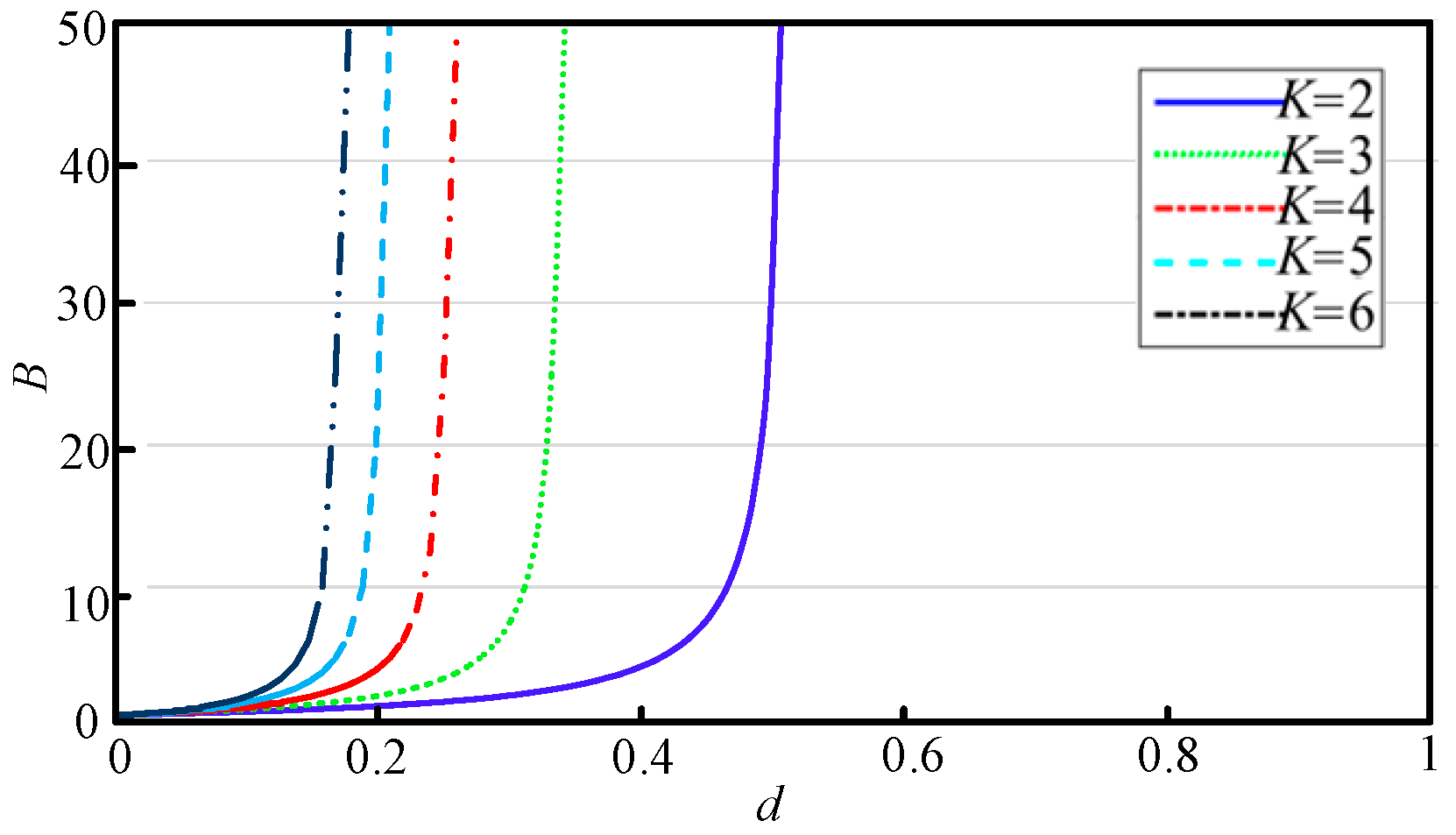
Figure 1. The deduction of Z-source networks: (a) Z-source; (b) qZ-source; (c) SI-qZ-source; (d) C-qZ-source.
Energies 17 02850 g001
Figure 2. The schematic of the new impedance source networks: (a) LCCT-source; (b) T-source; (c) Γ-source; (d) Δ-source; (e) Y-source.
Energies 17 02850 g002
Figure 3. The relationship between impedance source networks: (a) Y-source; (b) Γ-source; (c) LCCT-source; (d) T-source.
Energies 17 02850 g003
Figure 4. Schematic of the YSC.
Energies 17 02850 g004
Figure 5. Equivalent circuits of the YSC: (a) the ST state; (b) the NST state.
Energies 17 02850 g005
Figure 6. Relationship between YSC gain and duty cycle.
Energies 17 02850 g006
Figure 7. Schematic of qYSCs: (a) qYSC-I; (b) qYSC-II; (c) qYSC-III; (d) qYSC-IV.
Energies 17 02850 g007
Figure 8. Relationship between qYSC Gain and Duty Cycle: (a) qYSC-I; (b) qYSC-II; (c) qYSC-III; (d) qYSC-IV.
Energies 17 02850 g008
Figure 9. Schematic of the M-YSC.
Energies 17 02850 g009
Figure 10. Relationship between M-YSC Gain and Duty Cycle.
Energies 17 02850 g010
Figure 11. Equivalent circuits of the Y-source Converter Considering Leakage Inductance Effect: (a) Non-Shoot-Through state (NST); (b) Intermediate state; (c) Shoot-Through state (ST).
Energies 17 02850 g011
Figure 12. Expected waveforms for the voltage and current of YSC: (a) capacitive load; (b) indutive load.
Energies 17 02850 g012
Figure 13. Load arrangements: (a) capacitive load; (b) inductive load.
Energies 17 02850 g013
Figure 14. Schematic of the VD-qYSC: (a) VD-qYSC-I; (b) VD-qYSC-II.
Energies 17 02850 g014
Figure 15. Schematic of the LH-qYSCs: (a) LH-qYSC-I; (b) LH-qYSC-II; (c) LH-qYSC-III; (d) LH-qYSC-IV; (e) LH-qYSC-V; (f) LH-qYSC-VI.
Energies 17 02850 g015aEnergies 17 02850 g015b
Figure 16. Schematic of the HS-qYSCs: (a) HS-qYSC-I; (b) HS-qYSC-II; (c) HS-qYSC-III; (d) HS-qYSC-IV; (e) HS-qYSC-V; (f) HS-qYSC-VI.
Energies 17 02850 g016aEnergies 17 02850 g016b
Figure 17. Schematic of the DA-qYSCs.
Energies 17 02850 g017
Figure 18. Schematic of the HCS-qYSCs: (a) HSC-qYSC-I; (b) HSC-qYSC-II.
Energies 17 02850 g018aEnergies 17 02850 g018b
Figure 19. Y-source converter without DC magnetization current: (a) O-qYSC; (b) LCD-qYSC.
Energies 17 02850 g019
Figure 20. Schematic of the AC-qYSCs: (a) AC-qYSC-I; (b) AC-qYSC-II.
Energies 17 02850 g020
Figure 21. The Y-source converters combined with a boost converter: (a) CB-qYSC; (b) CB-M-YSC.
Energies 17 02850 g021
Figure 22. Schematic of the L-qYSC.
Energies 17 02850 g022
Figure 23. Schematic of the L-M-YSC.
Energies 17 02850 g023
Figure 24. The Relationship between Duty Cycle and Gain of Topology Structures mentioned above (K = 3, n = 1).
Energies 17 02850 g024
Figure 25. Schematic of the ZICR-YSC: (a) ZICR-qYSC; (b) ZICR-M-YSC.
Energies 17 02850 g025
Figure 26. Theoretical waveforms diagram of the ZICR-M-YSC: (a) theoretical waveforms I; (b) theoretical waveforms II..
Energies 17 02850 g026
Figure 27. Simulation results of branch current ripple.
Energies 17 02850 g027
Figure 28. Schematic of the CIF-M-YSC.
Energies 17 02850 g028
Figure 29. Schematic of the I-ZCS-YSC.
Energies 17 02850 g029
Figure 30. Schematic of the SH-M-YSC.
Energies 17 02850 g030
Figure 31. Theoretical waveforms diagram of the SH-M-YSC: (a) theoretical waveforms I; (b) theoretical waveforms II.
Energies 17 02850 g031
Figure 32. The simulation of the SH-M-YSC: (a) Y-source converters in hard switch mode; (b) Y-source converters in Soft Switch Mode.
Energies 17 02850 g032
Figure 33. The relationship between Vgs and Vds.
Energies 17 02850 g033
Figure 34. Efficiency of the different converters under different output power.
Energies 17 02850 g034
Table 1. Factors influencing the YSC boost ratio.
KdmaxBN1:N2:N3
21/2 ( 1 2 d ) 1 (1:1:3), (2:1:4), (1:2:5)
31/3 ( 1 3 d ) 1 (1:1:2), (3:1:3), (4:2:5)
41/4 ( 1 4 d ) 1 (2:1:2), (1:2:3), (5:1:3)
51/5 ( 1 5 d ) 1 (3:1:2), (2:2:3), (1:3:4)
61/6 ( 1 6 d ) 1 (4:1:2), (3:2:3), (2:3:4)
Table 2. Comparison of key parameters of impedance source network.
ClassTopologyBdmaxDegrees of Freedom
Class of Z-SourceZ-Source [8] ( 1 2 d ) 1 1 2 1
qZ-Source [12] ( 1 2 d ) 1 1 2 1
SI-qZ-Source [13] 1 + d 1 2 d d 2 2 1 1
C-qZ-Source [16] ( 1 ( 2 + n ) d ) 1 ( 2 + n ) 1 2
other coupled-inductance impedance Source convertersLCCT-Source [18] ( 1 ( 1 + n L Z ) d ) 1 ( 1 + n L Z ) 1 2
T-Source [19] ( 1 ( 1 + n T Z ) d ) 1 ( 1 + n T Z ) 1 2
Γ-Source [20] ( 1 ( 1 + 1 n Γ Z 1 ) d ) 1 ( 1 + 1 n Γ Z 1 ) 1 2
Δ-source [21] 1 + n 23 1 ( 2 + n 23 ) d ( 2 + n 23 ) 1 2
Class of Y-SourceY-Source [22] 1 1 K d 1 K 3
Table 3. The voltage gain of the M-YSC with different winding factor (K) and turns ratio.
KdmaxBN1:N2:N3
21(1 + 2d)/(1 − d)(1:1:3), (2:1:4), (1:2:5)
31(1 + 3d)/(1 − d)(1:1:2), (3:1:3), (4:2:5)
41(1 + 4d)/(1 − d)(2:1:2), (1:2:3), (5:1:3)
51(1 + 5d)/(1 − d)(3:1:2), (2:2:3), (1:3:4)
61(1 + 6d)/(1 − d)(4:1:2), (3:2:3), (2:3:4)
Table 4. Properties comparison among different impedance source networks.
ClassTopologyBdmaxContinuous Input CurrentInrush CurrentInductive VolumeSwitching Stress Component Voltage Stress
VC1, MAX
/Vin
VC2, MAX
/Vin
VD1, MAX
/Vin
VS, MAX
/Vin
Traditional Y-Source YSC
[22]
1 1 K d 1 K nohighbighigh ( 1 d ) B - ( K 1 ) B 1 1 K d
Quasi Y-sourceqYSC-II
[36]
1 1 ( 1 + K ) d 1 1 + K yeslowbighigh ( 1 d ) B K d B ( K 1 ) B 1 1 ( 1 + K ) d
qYSC-III
[38]
1 1 δ d 1 δ yeslowsmallhigh ( 1 d ) B ( δ 1 ) d B ( δ 1 ) B 1 1 δ d
Modified Y-SourceM-YSC
[39]
1 + K d 1 d 1yeslowbiglow 1 + K B 1 + K K B K 1 + K K 2 + K B + 2 K 1 + K d 1 1 d
Here, δ = (N1 + N2)/(N2N3).
Table 5. The voltages of coupled inductors in different states.
ModeVL
Non-Shoot-Through state V L ( N S T ) = n 12 n 12 + 1 ( V i n V C 1 )
Intermediate state V L ( I N T ) = { V L ( N S T ) n 12 n 12 + 1 ( V L 1 + V L 2 ) V L ( S T ) n 12 n 13 n 12 n 13 ( V L 3 V L 2 )
Shoot-Through state V L ( S T ) = n 12 n 13 n 12 n 13 V C 1
Table 6. The key Properties Comparison among Y-source converters with the absorbing circuit.
TopologyBILO,MAX/IinIS1,MAX/IinIS2,MAX/IinAverage Magnetizing Current
VD-qYSC-I [42] 1 δ 1 + ( δ 2 ) d - δ -high
LH-qYSC-I [44] 1 1 ( 1 + K ) d - δ -high
DA-qYSC [45] 1 1 ( 2 + K ) d + K d 2 1 δ -high
O-qYSC [47] 1 1 ( 2 + K ) d 1 δ -0
LCD-qYSC [48] 1 1 ( 1 + K ) d V C 3 L C D d T S L O δ -0
AC-qYSC-I [51] 1 1 2 ( 1 + K ) d - 0.5 δ 0.5 δ 0
Table 7. Other Properties Comparison among Different Y-source converters with the absorbing circuit.
TopologyVC1,MAX/VinVC2,MAX/VinVC3,MAX/VinVD1,MAX/VinVD2,MAX/VinVD3,MAX/Vin
VD-qYSC-I [42] ( 1 d ) 1 + ( δ 2 ) d ( d δ ) 1 + ( δ 2 ) d ( d 1 ) δ 1 + ( δ 2 ) d B 0 δ B δ 1
LH-qYSC-I [44] ( 1 d ) B ( δ 1 ) d B ( 1 ( δ 1 ) d ) B ( δ 2 ) B B -
DA-qYSC [45] ( 1 2 d ) B - ( 1 d ) B ( δ 2 ) B B ( δ 2 ) d B
O-qYSC [47] ( 1 2 d ) B ( δ 2 ) d B ( 1 d ) B ( δ 2 ) B B -
LCD-qYSC [48] ( 1 d ) B ( δ 1 ) d B V C 3 L C D ( δ 1 ) B ( 1 d ) B + V C 3 L C D V P N V C 3 L C D
AC-qYSC-I [51] ( 1 2 d ) B ( δ 2 ) d B B ( δ 2 ) B B B
Here, V C 3 L C D = 0.5 d B + 0.5 ( D B ) 2 + 4 L K L O I N 1 2 ( D T S V i n ) 2 .
Table 8. Properties Comparison among the Y-source converters combined with various boosting structures.
TopologyBVS,MAX/VinVD1,MAX/VinVD2,MAX/VinVC1,MAX/VinVC2,MAX/Vin
M-YSC [39] 1 + K d 1 d 1 1 d ( K 2 + 2 K ) ( 1 d ) + K ( 1 + K d ) ( 1 d ) 2 ( 1 + K d ) + K ( 1 d ) ( 1 + K ) ( 1 d ) ( 1 d ) + K ( 1 + K d ) ( 1 + K ) ( 1 d ) K ( 1 + K d ) K ( 1 d ) ( 1 + K ) ( 1 d )
CB-qYSC [52] 1 [ 1 ( 1 + K ) d ] ( 1 d ) 1 [ 1 ( 1 + K ) d ] ( 1 d ) ( d 1 d 1 ) K [ 1 ( K + 1 ) d ] ( 1 d ) 1 [ 1 ( K + 1 ) d ] ( 1 d ) K d ( 1 K d ) 1 d 1 K d
CB-M-YSC [33] 1 + d K ( 1 d ) 2 1 ( 1 d ) 2 1 + K 2 K d + K 2 d ( 1 d ) 2 1 ( 1 d ) 2 1 1 d ( 1 + K d 1 d ) K d ( 1 d ) 2
L-qYSC-I [53] 1 + d 1 ( 1 + K ) d K d 2 1 + d 1 ( 1 + K ) d K d 2 K ( 1 + d ) 1 ( 1 + K ) d K d 2 1 + d 1 ( 1 + K ) d K d 2 ( 1 + d ) ( 1 d ) 1 ( 1 + K ) d K d 2 ( 1 + d ) d K 1 ( 1 + K ) d K d 2
L-qYSC-II [53] 1 1 ( 2 + K ) d 1 1 ( 2 + K ) d K 1 ( 2 + K ) d 1 1 ( 2 + K ) d 1 d 1 ( 2 + K ) d d K 1 ( 2 + K ) d
L-qYSC-III [53] 2 + n 1 ( 1 + 2 K + n K ) d 2 + n 1 ( 1 + 2 K + n K ) d ( 2 + n ) K 1 ( 1 + 2 K + n K ) d 1 + n 1 ( 1 + 2 K + n K ) d ( 2 + n ) ( 1 d ) 1 ( 1 + 2 K + n K ) d ( 2 + n ) d K 1 ( 1 + 2 K + n K ) d
L-M-YSC-I [59] 1 + d K 1 d ( 1 + d ) 1 + d K 1 d 1 + d 1 d K 1 + d K 1 d d ( 1 + d ) 1 d K [ ( K 1 ) d + 1 ] 1 + d 1 d
L-M-YSC-II [59] 1 + d K 1 2 d 1 1 2 d K 1 2 d 1 1 2 d d K 1 2 d 1 d + d K 1 2 d
L-M-YSC-III [59] 1 + d K 1 d ( 2 + n ) 2 d 1 d ( 2 + n ) K 1 d ( 2 + n ) 1 + K d 1 d ( 2 + n ) d K 1 d ( 2 + n ) 1 d d K 1 d ( 2 + n )
Here, n is the turns ratio of the switch-coupled inductance.
Table 9. Properties Comparison among the typical topologies with low input current ripple.
TopologyBVS,MAX/VinInput Current RippleComponent Count
Magnetic CoresDCS
YSC 1 + K d 1 d 1 1 + K d B d V i n L f 2231
[64] 1 + K d 1 d 1 1 + K d B 02241
[65] 1 + d + n d ( 1 d ) 2 1 1 + d + n d B 03441
[66] 1 + ( n 2 + n 3 ) d 1 d 1 1 + ( n 2 + n 3 ) d B ( N 4 N 1 ) 2 C 4 L l k 4 V i n + π 2 V i n L m L l k 4 C 4 + N 3 N 1 I D 1 ( t 0 ) 1441
[67] n + 2 1 d 1 n + 2 B d V i n L f 2242
Table 10. Properties Comparison among the Y-source converters.
TopologyBVS,MAX/VinSoft SwitchingFrequency (kHz)Component Count
CLCoupled InductorD
[39] 1 + K D 1 D 1 1 D -100311 (3w)2
[64] 1 + K D 1 D 1 1 D -50421 (3w)2
[69] 1 + K D 1 D 1 1 D ZVS + ZCS500311 (3w)2
Disclaimer/Publisher’s Note: The statements, opinions and data contained in all publications are solely those of the individual author(s) and contributor(s) and not of MDPI and/or the editor(s). MDPI and/or the editor(s) disclaim responsibility for any injury to people or property resulting from any ideas, methods, instructions or products referred to in the content.

