Article

A Collaborative Modulation Method of Dual-Side Backflow Power Optimization and Zero-Voltage Switching for Dual Active Bridge

1
School of Electrical and Information Engineering, Tianjin University, Tianjin 300072, China
2
School of Information Engineering, Nanchang University, Nanchang 330031, China
3
Foshan Power Supply Bureau, Guangdong Power Grid Co., Ltd., Foshan 528000, China
*
Author to whom correspondence should be addressed.
Energies 2024, 17(12), 3019; https://doi.org/10.3390/en17123019
Submission received: 11 April 2024 / Revised: 11 May 2024 / Accepted: 13 May 2024 / Published: 19 June 2024
(This article belongs to the Special Issue Power Electronic and Power Conversion Systems for Renewable Energy)

Abstract

:
Dual active bridge (DAB) converters are widely used in DC microgrids because of their superior bidirectional energy flow regulation capability and characteristics, such as wide voltage gain and zero-voltage switching (ZVS). However, due to the inherent contradiction between the minimum backflow power and the ZVS of the power switches, the existing modulation methods are difficult to optimize and coordinate. Most of the studies increase the complexity of energy flow regulation in the optimization process. To solve the above problems, this paper proposes a collaborative modulation method of dual-side backflow power optimization and ZVS for DAB. The method constructs a dual-side backflow power optimization modulation strategy that is simple to control and uniform in all working conditions by analyzing the mathematical model of backflow power. Meanwhile, based on this optimized modulation strategy, a regulatory factor of phase-shift ratio is introduced to collaborate with the ZVS of the power switches, which reduces the backflow power while ensuring the ZVS of the primary and secondary sides. Finally, a 500W DAB prototype is built, and the experimental results verify the feasibility and effectiveness of the proposed modulation method.

1. Introduction

As the scale of energy utilization for social production and life continues to expand, traditional fossil energy sources such as coal and oil are gradually depleted, environmental pollution is becoming increasingly serious, and global climate change is intensifying. These make environmentally friendly renewable energy receive widespread attention [1]. DC microgrids have been rapidly developed due to high energy utilization and the ability to accommodate renewable energy generation and multiple types of loads [2]. As the main link of energy regulation, the energy router plays a pivotal role in DC microgrids [3]. In addition, the change in energy structure also promotes the development of Electric Vehicles (EVs). It not only effectively alleviates the tension of fossil energy but also serves as an energy storage system that can interact with the grid to smooth out the peak–valley difference in the grid [4].
The energy router requires DC-DC converters to realize the energy interaction between different ports. For EVs, the architecture of on-board chargers (OBCs) generally consists of an AC-DC converter with power factor correction (PFC) followed by a DC-DC converter. The AC-DC converter is responsible for the energy conversion between the AC grid side and the DC side. The DC-DC converter completes the energy interaction between the output of the AC-DC converter and the EV’s battery to realize the charging of the battery or the vehicle-to-grid (V2G) function [5,6,7]. In addition, the EV’s auxiliary loads need to obtain power from the high-voltage lithium-ion battery through the auxiliary power modules (APMs). And the voltage level of these auxiliary loads is low, which requires the use of DC-DC converters to realize the energy conversion between the high-voltage side and the low-voltage side [8]. In summary, the energy router, OBC, and APM of the EV all need DC-DC converters to realize the energy conversion between different voltage levels and the control of bidirectional energy transfer. In addition, electrical isolation between the two ends is also required in consideration of the electrical safety, reliability, and fault tolerance of the power system. For bidirectional isolated converters, the two most widely researched and promising topologies are the DAB converter and the CLLC resonant converter [9,10].
Compared with the CLLC resonant converter, the DAB converter was proposed earlier and the related research is more mature. The DAB converter has a simple structure with fewer components, which is easy to analyze. And the voltage and current of the DAB converter vary linearly in all stages. In the steady-state analysis, the analytical expression can be obtained easily by the method of segmental solution. At the same time, according to the results of steady-state analysis, various dynamic models such as the reduced-order model and discrete-time full-order model can be established to facilitate the design and implementation of the controller [8]. Also, DAB can easily realize the regulation of the value and direction of the energy flow by adjusting the phase-shift angle, which has a great advantage in the ability of bidirectional energy transfer. As for the CLLC resonant converter, as a fifth-order system with strong nonlinearity, the modeling of its circuit is more complicated and has higher computational requirements. Although there has been related research to simplify the modeling process, it has not been possible to change the nature of the approximate solution or numerical solution [11]. In addition, the complexity of CLLC resonant converter control is higher compared to the DAB converter. And the CLLC resonant converter usually uses the pulse frequency modulation (PFM) method. Its disadvantage is the wide operating frequency range, which leads to first harmonic approximation errors, high switching losses, and a narrow operating voltage range. For this reason, it is necessary to design hybrid control methods to avoid these drawbacks [9]. Meanwhile, the CLLC resonant converter has a more prominent output current surge problem during startup, and the necessary soft-start control is required to suppress the output surge current. To improve the operating efficiency of the CLLC resonant converter, it is generally necessary to design a higher quality factor. This results in a smaller resonant capacitance with higher voltage stress, which is susceptible to aging under the action of larger resonant currents. Additionally, the power switches on the secondary side cannot be turned off during operation, which means that the length of its dead time needs to be controlled. Therefore, it is necessary to design the corresponding synchronous rectification scheme. Both the DAB converter and the CLLC resonant converter have better bidirectional soft-switching characteristics, but the soft-switching range of the CLLC resonant converter is wider. Moreover, the leakage inductance of the CLLC resonant converter is smaller, and the backflow power flowing through the circuit is lower than that of the DAB converter [4]. In summary, the circuit modeling of the CLLC resonant converter is more complicated, and there are control problems such as wide frequency adjustment range, soft-start, and synchronous rectification, which makes the control implementation more difficult. In contrast, DAB has a simple structure, easy circuit modeling, strong directional energy transfer capability, and more mature academic research and practical application. Its disadvantage lies in the soft-switching range and backflow power, but this can be solved by the PWM modulation method. Therefore, this paper further explores the soft switching and backflow power of the DAB converter.
DAB converters usually use phase-shift modulation, which can be further categorized into single-phase-shift (SPS) modulation [12], extended-phase-shift (EPS) modulation [13], dual-phase-shift (DPS) modulation [14], and triple-phase-shift (TPS) modulation [15], depending on the phase-shift angle involved. SPS modulation can control the magnitude and direction of the output power by adjusting the phase-shift angle between the primary and secondary H-bridges. Although it is easy to realize the regulation of energy flow, it cannot reduce the backflow power [16].
Various optimization modulation methods have been proposed to suppress the backflow power. J. Tian et al. in [17] integrate the backflow and transmission power into a unified integral function based on EPS modulation and optimize the backflow power with a fully differential algorithm. However, this method requires solving a large number of differentials and partial derivatives online, which is computationally intensive. H. Shi et al. construct a mathematical model of the backflow power for EPS and solve the optimal phase-shift ratio combination by the Karush–Kuhn–Tucker (KKT) condition in [18]. Although this study provides an accurate analysis of the backflow power with an optimization algorithm, the ZVS of the power switches is not considered in the backflow power optimization process. In [19], to collaborate with ZVS during the backflow power optimization, the conditions for the realization of the ZVS are investigated by analyzing the output capacitors’ charging and discharging process and the power switches’ dead zone. The DAB converter’s ZVS and minimum primary-side backflow power are realized by controlling the inductor current when the power switch is turned on. However, the modulation methods studied above are all based on EPS. Although the backflow power on one side can be suppressed by adjusting the internal phase-shift angle, it cannot optimize the backflow power on the other side where the internal phase-shift angle is not introduced.
To optimize the dual-side backflow power of the DAB, an internal phase-shift angle at both the primary and secondary sides must be introduced. Since DPS belongs to a special case of TPS [20], many researchers directly investigate the optimization of backflow power based on the more complex TPS modulation. In [21], the optimal phase-shift ratio for minimum reactive power under TPS modulation is discussed. However, its optimization process is based on the simplified derivation of graphs rather than on the mathematical model solution of backflow power, and the two are not strictly equivalent. S. Wang et al. [22] define the reactive current, reactive power, and power factor of the DAB in the time domain to reduce the backflow power by optimizing the global power factor. However, the classification of reactive currents is based on intuitive time-domain analysis results rather than strictly mathematical logic. In addition, these two studies only focus on the backflow power suppression of TPS and do not involve the exploration of the ZVS. In contrast, S. Li et al. [23] select four operation modes of TPS modulation and obtain the optimization modulation curve of the backflow power by solving the condition that the backflow power in different power regions is zero. Based on this, the ZVS is realized by introducing a weight coefficient of the phase-shift ratio. However, it does not optimize the backflow power in the high-power range, and the optimization modulation methods at boost and buck state are incompatible, which is not conducive to the energy flow regulation in DC microgrids. For the optimization of backflow power under full operation conditions, a multi-objective optimization model is constructed by analyzing four operation modes of TPS and solved accurately with the particle swarm optimization algorithm in [24]. This optimization process is completed offline, and no explicit unified modulation method is given. Moreover, it needs to be recalculated when the parameters change, making it difficult to adapt to the changing working conditions in practical applications.
In addition, asymmetric phase-shift modulation with a non-50% duty cycle of the drive signals has been used to increase the degree of freedom of DAB control [25]. In [26], an asymmetric duty cycle and internal phase-shift modulation method is proposed to eliminate the backflow power at a light load. However, it does not optimize the dual-side backflow power over the full operation range and does not consider the ZVS. The asymmetric phase-shift modulation strategy is also used to achieve ZVS over the full power range and greatly improves the light-load efficiency [27]. However, it still fails to eliminate the phase in which the peak inductor current is opposite in polarity to the primary H-bridge voltage during the switching cycle. This makes the backflow power of the asymmetric phase-shift modulation larger.
To solve the problems of the collaborative implementation of the dual-side backflow power optimization and the ZVS for DAB in the above modulation methods, and to ensure the simplicity of the energy flow regulation as much as possible, this paper proposes a collaborative modulation method of dual-side backflow power optimization and ZVS. This paper mainly considers two aspects of research: On the one hand, based on the TPS modulation method, the dual-side backflow power is optimized for different voltage gains in the full load power range. At the same time, considering the simplicity of the converters’ control implementation, a full-operation-range dual-side backflow power optimization modulation method for DAB is designed. The modulation method not only achieves the optimization of dual-side backflow power over the full load power range but also is unified under different voltage gains. Meanwhile, the relationship between the output power and the internal phase-shift ratio of the primary-side H-bridge is monotonic in this method, which is very convenient for controlling energy flow. On the other hand, to realize the ZVS for all power switches, a ZVS collaborative method based on dual-side backflow power optimization is designed. The modulation method realizes the ZVS for both primary-side and secondary-side power switches by introducing a phase-shift ratio regulatory factor while optimizing the dual-side backflow power.
The rest of the paper is organized as follows. Section 2 analyzes the backflow power of TPS modulation. The proposed collaborative modulation method of dual-side backflow power optimization and ZVS is described in Section 3. Then, Section 4 presents comprehensive experimental results to validate the effectiveness and rationality of the proposed modulation method. Conclusions are drawn in Section 5.

2. Backflow Power Analysis of TPS Modulation

The topology of a typical DAB converter is shown in Figure 1. In Figure 1, Q1P~Q4P constitute the primary-side full-bridge inverter, and Q1S~Q4S make up the secondary-side full-bridge rectifier. Tr is a high-frequency isolated transformer with turns ratio n, Lr is its leakage inductance, and Cin1 and Co1 are filter capacitors. Vin1 and Vo1 are the input voltage and output voltage. iin1 and io1 are the input current and output current. vab and vcd represent the voltages at the midpoint of the primary and secondary H-bridges. During the switching cycle, reactive circulating power is generated when the voltages at the midpoint of the primary and secondary H-bridges are opposite in polarity to the inductor current, which is defined as the backflow power.
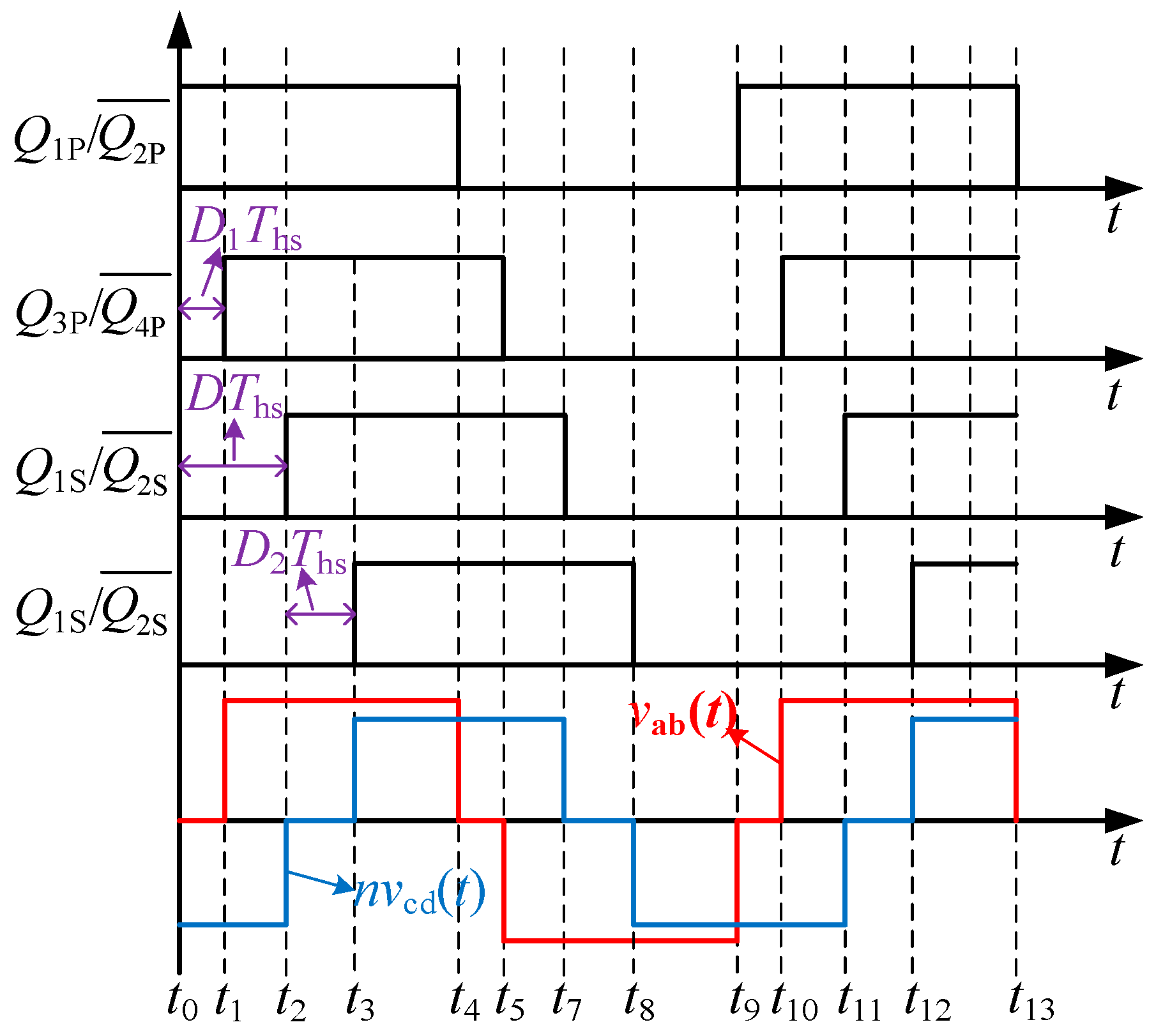
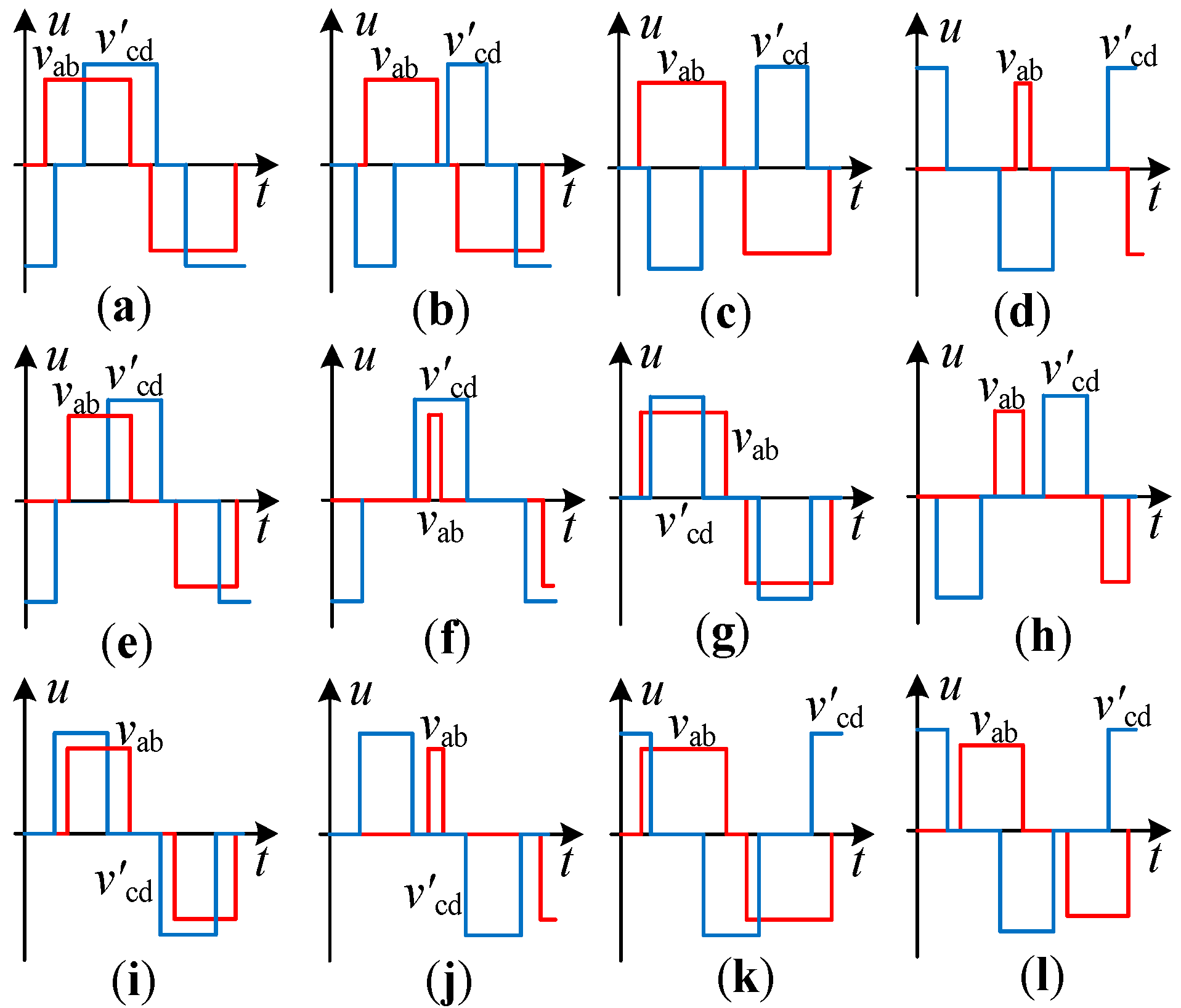
To achieve the optimization of backflow power, the TPS modulation method is used in this paper. It consists of three control variables: D is the external phase-shift ratio between the primary and secondary H-bridges; D1 is the internal phase-shift ratio of the primary H-bridge; and D2 is the internal phase-shift ratio of the secondary H-bridge, as shown in Figure 2. Both D and D1 are referenced to Q1P/Q2P, while D2 is referenced to Q1S/Q2S. In this way, the pulse voltage widths of vab and vcd can be changed by adjusting D1 and D2, and the phase-shift angle of vab and vcd can be changed by adjusting D. Depending on the different constraint relationships of D, D1, and D2, there are different combinations of D, D1, and D2, which in turn make vab and vcd exhibit different characteristics and affect the trend of inductor current iL. Accordingly, the TPS modulation can be divided into various operation modes, as shown in Figure 3. In this paper, v cd is the value of vcd converted to the primary side of the transformer, iL is the current of Lr, and the voltage gain of the DAB is defined as k = Vin1/(nVo1). Ths is the half switching period, and fs is the switching frequency.
Due to the symmetry between the working conditions of DAB forward energy transfer and reverse energy transfer, to simplify the analysis process, the operation modes with forward energy transfer are selected for optimization in this paper. In Figure 3, the power transfer direction in Mode I-L is reversed, and the range of D is less than zero [28]. Therefore, these modes will not be discussed in this paper. The turn-on moment of the power switch Q1P in Figure 2 is defined as t0. To realize the ZVS of the primary and secondary power switches, it is necessary to satisfy the relationship shown in (1).
i L ( t 0 ) < 0 i L ( t 0 + D 1 T h s ) < 0 i L ( t 0 + D T h s ) > 0 i L ( t 0 + D 2 T h s + D T h s ) > 0
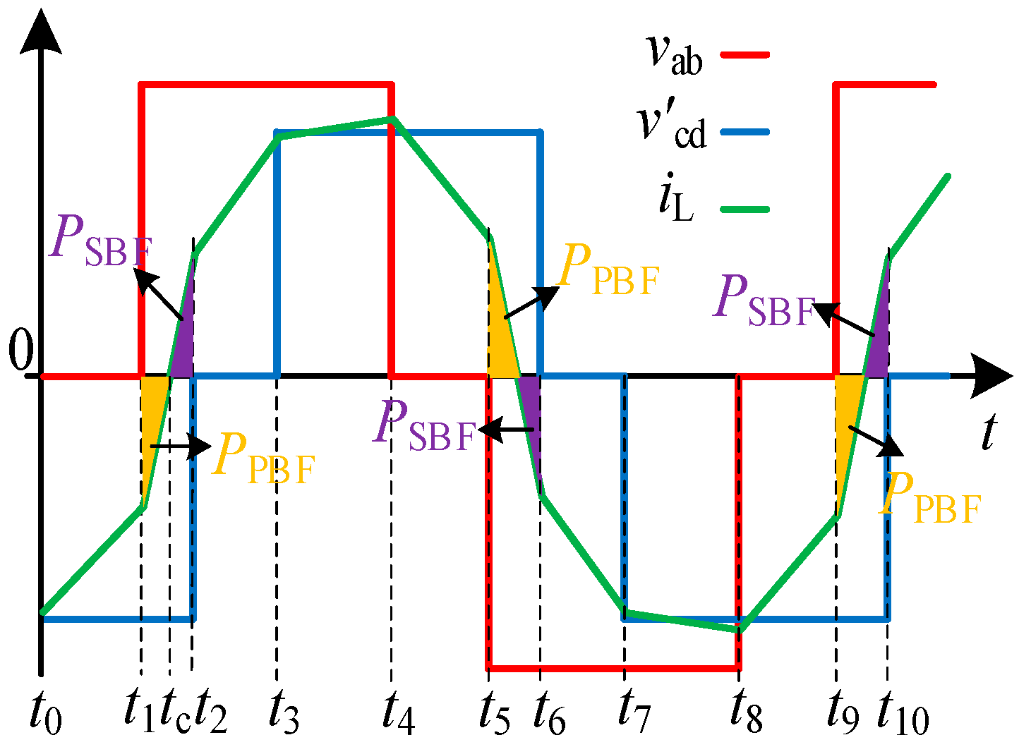
And when D < D1, there is iL(t0 + D1Ths) = iL(t0 + DThs), and the relationship shown in (1) is no longer satisfied. At this time, there must be a pair of power switches in Q3P/Q4P and Q1S/Q2S that cannot realize ZVS. Therefore, to realize the ZVS for all power switches of DAB, it is necessary to further exclude Mode E-H. In Mode C and Mode D, the polarity of vab and v cd in the half cycle is reversed, which will make their backflow power larger compared to Mode A and Mode B. Therefore, Mode C and Mode D are not taken into account in the backflow power optimization. Although Mode A and Mode B are applicable for k < 1 and k > 1, Mode A has a wider range of transmitted power than Mode B. In this paper, to meet the demand of wide-range power transmission, Mode A is selected as the main operation mode of DAB for the backflow power optimization. For Mode A, the voltage and current waveforms and the primary and secondary backflow power are shown in Figure 4. The constraint relationship between the three control variables in Mode A is shown in (2).
0 D 1 D D + D 2 1
In Figure 4, based on the operation characteristics of the inductor and the symmetry of the positive and negative half cycles of the waveforms, the current value of the leakage inductance current iL in Mode A at the moments of t0, t1, and t2 can be obtained as shown in (3).
i L ( t 0 ) = n V o 1 ( 1 2 D D 2 k + k D 1 ) 4 L r f s i L ( t 1 ) = n V o 1 ( 1 2 D + 2 D 1 D 2 k + k D 1 ) 4 L r f s i L ( t 2 ) = n V o 1 ( 1 D 2 k k D 1 + 2 k D ) 4 L r f s i L ( t 3 ) = n V o 1 ( 1 D 2 k k D 1 + 2 k D + 2 k D 2 ) 4 L r f s
And based on the half-cycle current waveform shown in (3), the normalized output power P o _ A * in Mode A can be further obtained, as shown in (4).
P o _ A * = 2 2 D 2 D 1 2 D 2 2 + 2 D D 1 + D 2 + 2 D D 1 2 D D 2 + D 1 D 2
Thus, the normalized value of the dual-side backflow power P BF _ A * can be further obtained, as shown in (5).
P BF - A * = 1 2 k ( k + 1 ) k ( 1 2 D + 2 D 1 D 2 ) k ( 1 D 1 ) 2 + ( 1 D 2 ) k ( 1 + D 1 2 D ) 2
From (3), we can see that iL(t0) < iL(t1) and iL(t2) < iL(t3). Therefore, according to (5), to realize the ZVS of the primary and secondary power switches in Mode A, it is sufficient to satisfy iL(t1) < 0 and iL(t2) > 0. And the ZVS condition of Mode A is shown in (6).
( k + 2 ) D 1 2 D D 2 k + 1 < 0 k D 1 2 k D + D 2 + k 1 < 0

3. The Proposed Collaborative Modulation Method of Dual-Side Backflow Power Optimization and ZVS for DAB

3.1. Full-Operation-Range Dual-Side Backflow Power Optimization Modulation Method

According to (5), the backflow power has a minimum value of zero when D, D1, and D2 satisfy the relationship shown in (7).
D 1 = D D 2 = 1 - k + k D
With the relationship between the phase-shift ratios shown in (7), the normalized value of the DAB output power P o _ op 1 * can be expressed as
P o _ op 1 * = 2 [ ( k 2 + k + 1 ) D 2 2 k 2 D + k 2 k ]
According to (8), the maximum output power that can be achieved by DAB with the relationship between the phase-shift ratios shown in (7) can be deduced as
P o _ max _ op 1 * = 2 k k 2 + k + 1
Analyzing (9), it can be obtained that when the output power of DAB increases to a certain value, the backflow power cannot be regulated to zero through the relationship shown in (7). To optimize the backflow power when the output power is in the power interval ( P o _ max _ op 1 * , 1), this paper establishes an optimization problem for solving the minimum backflow power with the DAB transmission power as the equation constraint and the boundary range of Mode A and the ZVS condition as the inequality constraint. The backflow power at larger power can be reduced by preferring the combination of phase-shift ratios (D, D1, D2) for this interval. The optimization problem can be described as
min P BF - A * ( D , D 1 , D 2 ) s . t . : P o _ A * ( D , D 1 , D 2 ) = P o * ; i L ( t 1 ) < 0 , i L ( t 2 ) > 0 ; 0 < D 1 D D + D 2 1 .
Since the optimization problem shown in (10) contains inequality constraints, the KKT condition is chosen to solve it, as shown in (11).
L = k ( 1 2 D + 2 D 1 D 2 ) k ( 1 D 1 ) 2 + ( 1 D 2 ) k ( 1 + D 1 2 D ) 2 2 k ( k + 1 ) + λ [ 2 ( 2 D 2 D 1 2 D 2 2 + 2 D D 1 + D 2 + 2 D D 1 2 D D 2 + D 1 D 2 ) P o * ] + μ 1 [ ( k + 2 ) D 1 2 D D 2 k + 1 ] + μ 2 ( k D 1 2 k D + D 2 + k 1 ) + μ 3 ( D 1 ) + μ 4 ( D 1 D ) + μ 5 ( D 2 ) + μ 6 ( D + D 2 1 ) . L D = 0 , L D 1 = 0 , L D 2 = 0 , μ 1 [ ( k + 2 ) D 1 2 D D 2 k + 1 ] = 0 , μ 2 ( k D 1 2 k D + D 2 + k 1 ) = 0 , μ 3 ( D 1 ) = 0 , μ 4 ( D 1 D ) = 0 , μ 5 ( D 2 ) = 0 , μ 6 ( D + D 2 1 ) = 0 , μ i 0 ( i = 1 , , 6 ) , 2 ( 2 D 2 D 1 2 D 2 2 + 2 D D 1 + D 2 + 2 D D 1 2 D D 2 + D 1 D 2 ) P o * = 0 , ( k + 2 ) D 1 2 D D 2 k + 1 < 0 , k D 1 2 k D + D 2 + k 1 < 0 , 0 < D 1 D D + D 2 1 .
Thus, the optimal phase-shift ratio combination (D, D1, D2) to optimize the backflow power in the high-power range can be found, as shown in (12).
D 1 = k 2 D 2 D = 1 2 + k 2 k 1 2 D 2
With the relationship shown in (12), the normalized value of the DAB output power P o _ op 2 * and the normalized value of the dual-side backflow power P bf _ op 2 * can be expressed as
P o _ op 2 * = 1 D 2 2 ( k 4 + k 2 + 1 ) P bf _ op 2 * = k 3 + 1 2 k ( k + 1 ) ( 1 D 2 k 2 D 2 k D 2 ) 2
Furthermore, the fact that Mode A needs to satisfy the conditional constraints shown in (2) makes the range of the phase-shift ratio D limited, as shown in (14). Combined with (4), it can be seen that this will prevent the optimization modulation method shown in (7) from being extended to regions of low output power. Therefore, the dual-side backflow power in the low-power range cannot be regulated to zero in Mode A.
max 0 , 1 1 k D 1 1 k + 1
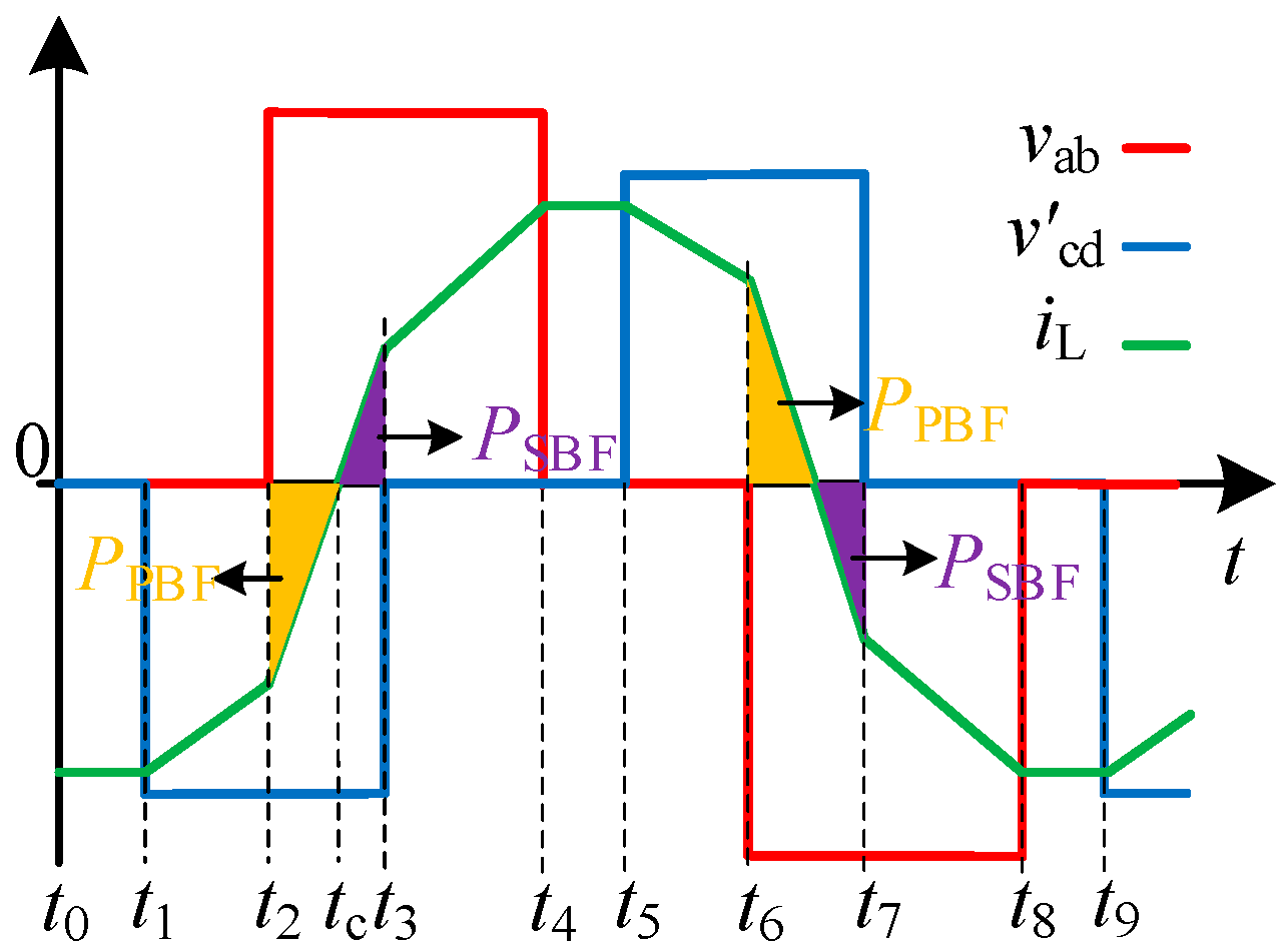
To explore the optimization modulation method of backflow power in the low-power range, Mode B is selected for further investigation based on the above analysis of each mode of the TPS modulation. The voltage and current waveforms and the primary and secondary backflow power in Mode B are shown in Figure 5, and the constraints in this mode can be expressed as
0 D + D 2 1 D 1 D 1
By analyzing Figure 5, the normalized output power P o _ B * in Mode B can be obtained, as shown in (16).
P o _ B * = 2 ( D 1 2 D 2 D 1 D 2 + 2 D D 1 + D 1 D 2 + 1 )
And the normalized dual-side backflow power and ZVS constraints in Mode B are the same as those in Mode A, as shown in (5) and (6). Therefore, the backflow power in Mode B can also be regulated to zero by the phase-shift ratio relationship shown in (7). In this case, the normalized output power of DAB P o _ op 3 * can be expressed as
P o _ op 3 * = 2 k ( 1 D ) 2
Based on the constraints of Mode B shown in (15), the output power range of DAB with the relationship shown in (7) can be deduced as
0 P o _ op 3 * 2 k ( k + 1 ) 2
According to (18), it can be seen that the backflow power in the low-output-power range of the DAB can be optimized in Mode B. At the same time, to facilitate the practical control of DAB, it is necessary to find a control variable about which the output power is monotonically varying. From (12), the monotonicity of the output power with respect to the phase-shift ratio D in the high-power range presents different characteristics at different voltage gains. But in the optimization results of the high-power range and the low-power range, both D1 and D2 decrease gradually with the increase in the output power. Meanwhile, there is D1 = D in the low- and medium-output-power range. And in the backflow power optimization results, D and D2 can establish a direct connection with D1. Therefore, this paper chooses D1 as the control variable of the optimization modulation method. In this way, the amplitude and direction of the DAB converter’s output power can be regulated by controlling the value of D1. In addition, to ensure the continuity of D1 and the backflow power optimization over the full load power range, the variation interval of D1 in the medium-power range is set to be [k2/(k2 + k + 1), 1 − 1/(k + 1)]. Then, the dual-side backflow power optimization modulation results for DAB forward power transfer can be obtained, as shown in Table 1, where P o * is the normalized output power, and P BF * is the normalized dual-side backflow power.
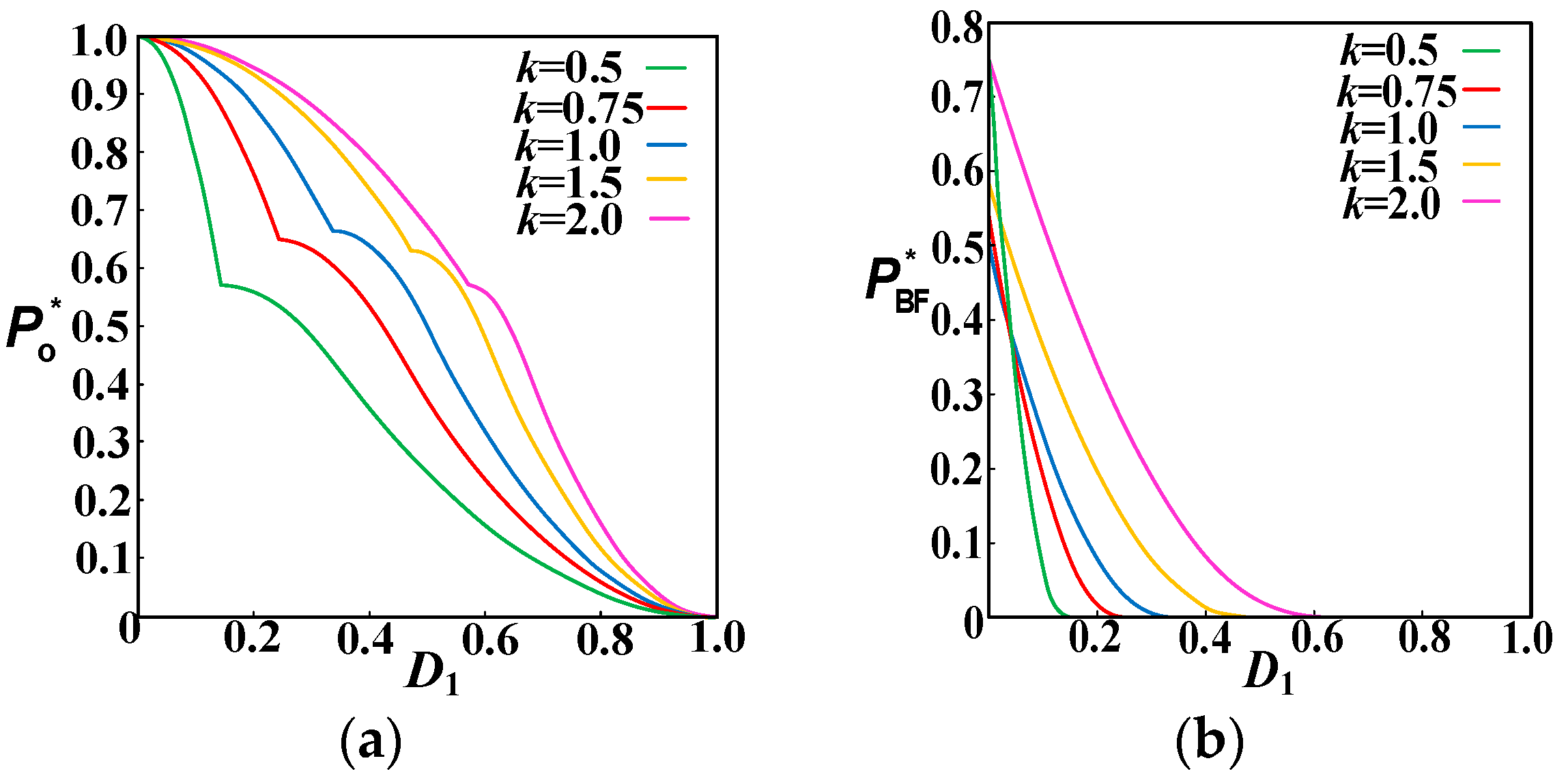
As can be seen from Table 1, the optimization modulation results for the dual-side backflow power are divided into three segments according to the load power range. Based on the optimization modulation results, the relationship curves between the output power P o * , the backflow power P BF * , and the control variable D1 at five different voltage gains are drawn in Figure 6. Analyzing Figure 6a, it can be obtained that as D1 decreases, the output power P o * gradually increases and always varies continuously. This shows the feasibility of choosing D1 as the control variable.
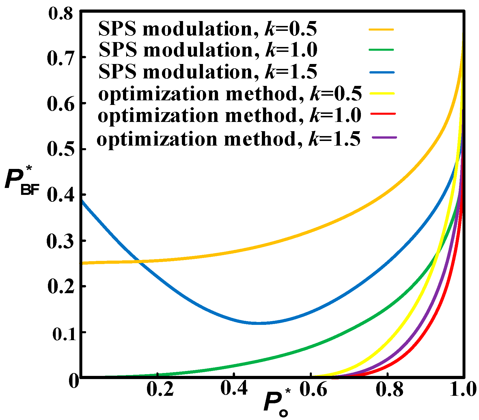
And Figure 6b shows that the designed backflow power optimization modulation method reduces the backflow power to zero in the low- and medium-output-power range. However, in the high-power-output range, the backflow power also shows a rising trend with the rise in output power, and the range of this region and the magnitude of the power are related to the voltage gain k. Combined with the analysis of the dual-side backflow power during SPS modulation, a plot of backflow power versus output power for the two modulation methods at different voltage gains can be drawn, as shown in Figure 7. It shows that the optimization modulation method reduces the backflow power over the full operation range compared to the SPS modulation, whether the DAB is operated in the boost stage or in the buck stage.
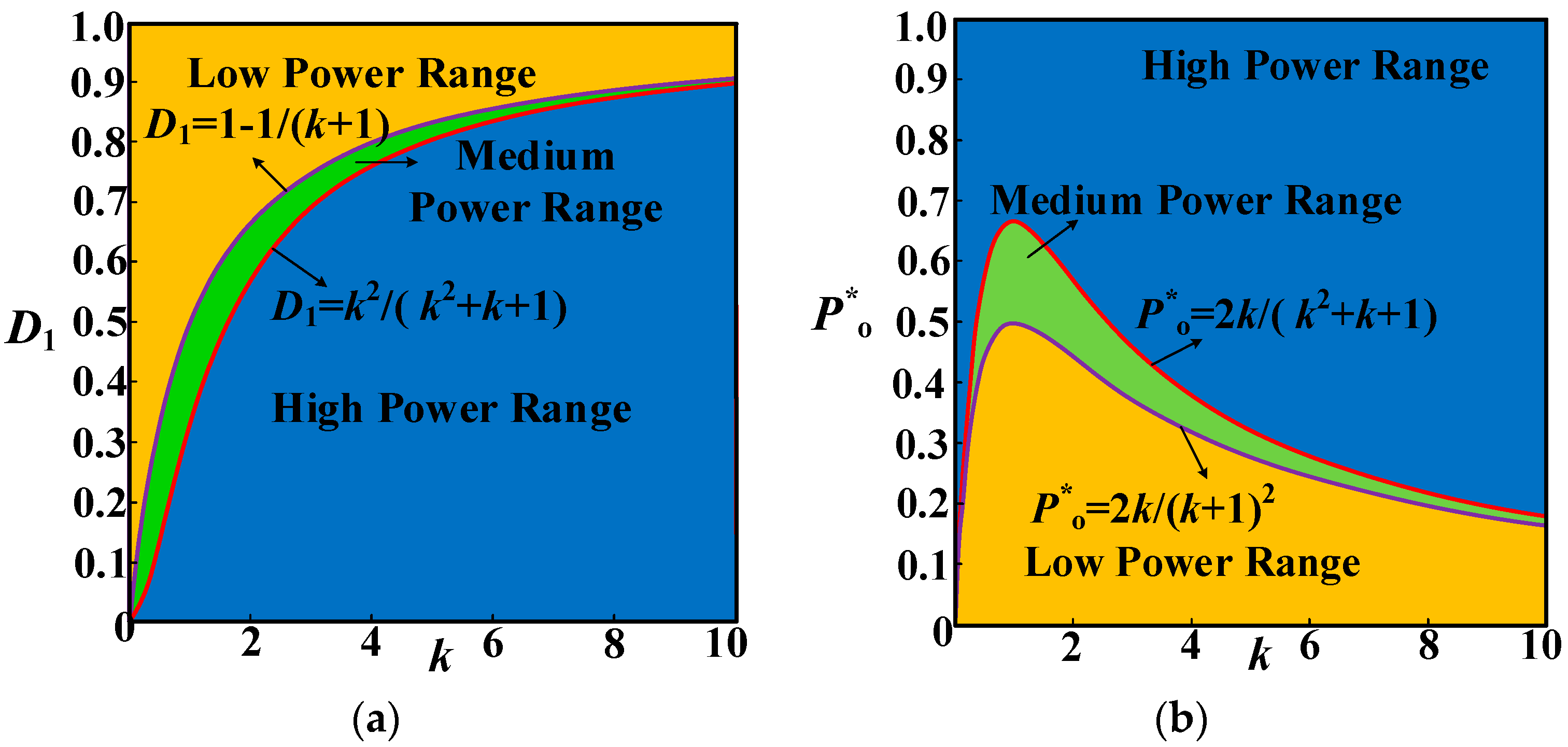
In addition, as shown in Figure 8, the power range of each segment of the optimization curve varies with the voltage gain k. However, the designed optimization modulation method can meet the requirements of different voltage gains and can cover the positive full load power range at different voltage gains. Combined with the above analysis, based on the phase-shift ratio relationship shown in Table 1, the output power regulation can be achieved by adjusting D1, while the dual-side backflow power can be optimized for the full operation range in the forward direction.
According to the above analysis of the forward energy flow, the dual-side backflow power modulation results can be extended to the region of the reverse energy flow based on the symmetry and the periodicity of the drive signal, and then a continuous dual-side backflow power optimization modulation curve in the full range of operating conditions can be obtained, as shown in (19).
D = 1 2 + k 2 k 1 2 k 2 D 1 , D 2 = D 1 k 2 , w h e n 0 D 1 < k 2 k 2 + k + 1 ; D = D 1 , D 2 = 1 k + k D 1 , w h e n k 2 k 2 + k + 1 D 1 < k 2 + 2 k + 2 k 2 + k + 1 ; D = 3 2 k 2 k 1 2 k 2 ( 2 D 1 ) , w h e n D 2 = 2 2 D 1 k 2 , k 2 + 2 k + 2 k 2 + k + 1 D 1 2 .

3.2. ZVS Collaborative Method Based on Backflow Power Optimization

In the optimization analysis of the backflow power in the previous section, the determination of ZVS is based on the positive and negative inductor currents when the power switch is turned on. Although this determination method is simple, due to the existence of the output capacitance of the power switch itself, this method cannot completely guarantee the ZVS. To realize the ZVS of a power switch, in addition to meeting the conditions shown in (6), it is also necessary that the current value IL flowing through the inductor at the instant of the power switch turn-on meets the relationship shown in (20) [19].
I L V 2 C oss L r
where V is the voltage of the power switch, the value of which can be determined according to its location; Coss is the output capacitance of the power switch. According to (20), if the ZVS is to be realized, the dual-side backflow power cannot be completely optimized to zero, and a small portion of the backflow power needs to exist to realize the charging and discharging of Coss. For this reason, this paper refines the optimization results for the dual-side backflow power with the condition shown in (20) on the premise of achieving ZVS. In Mode A and Mode B, to satisfy the ZVS of the primary and secondary power switches, the relationship shown in (21) needs to be satisfied.
i L ( t 0 + D 1 T h s ) V in 1 2 C oss L r i L ( t 0 + D T h s ) V o 1 n 2 C oss L r
Obviously, with the optimization modulation curve shown in (19), there is a relation D1 = D in the low- and medium-power range, which makes iL(t0 + D1Ths) = iL(t0 + DThs) = 0. And it results in the backflow power in this power range being optimized to zero, and the ZVS cannot be implemented. To satisfy (21), a regulatory factor λ with a small value is introduced so that there is D = D1 + λ in the low- and medium-power range, while the relationship between D2 and D remains unchanged. Accordingly, the condition for λ can be further obtained, as shown in (22).
λ 8 k L r f s k + 2 2 C oss L r λ 4 L r f s n 2 k 2 C oss L r
As can be seen from (22), when λ is larger than a certain value, the ZVS condition can be satisfied in the low- and medium-power range. In the high-power range, as the output power rises, the backflow power gradually increases from zero, and the backflow power of the primary side is k3 times the backflow power of the secondary side. Therefore, as long as (21) is satisfied in the initial region of low backflow power, the ZVS can be realized in the whole high-power range. And since the region of lower backflow power in the high-power range is adjacent to the medium-power range, the ZVS of the power switches in the high-power range can be realized by extending the action region of λ by a small portion in the direction of high power.
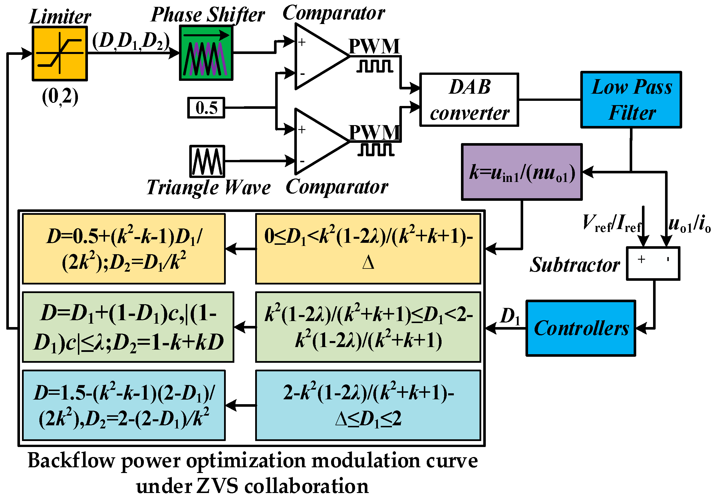
In order to ensure the continuity of the phase-shift ratio and the unity of the optimization modulation method as much as possible, the position of the switching from the medium-power range to the high-power range under the ZVS condition is chosen to be D1 = k2(1 − 2λ)/(k2 + k + 1). To facilitate the realization of the control, a small hysteresis interval is added for the discontinuity of D2 during the switching. At the same time, the addition of the regulatory factor λ in the low-power range results in an optimization modulation curve that does not pass through D = D1 = D2 = 1. It leads to discontinuities when switching between forward and reverse energy flows. Considering that iL is small when the output power is very low, it is difficult to satisfy the requirement of (21). Therefore, this paper chooses to prioritize the requirement of the continuity of the modulation curve in the region near the zero point of the output power. And a small adjustment factor c is introduced in this paper to set D = D1 + (1 − D1)c in this region, while the relationship between D2 and D is still kept as D2 = 1 − k + kD. Meanwhile, a limiter with the value of λ is added to (1 − D1)c to ensure its automatic continuity with the subsequent modulation curve. Then, it is extended to the reverse energy flow region according to the symmetry, which can form the control structure based on the collaborative modulation method of dual-side backflow power optimization and ZVS, as shown in Figure 9. According to Figure 9, the backflow power optimization under ZVS collaboration designed in this paper is realized by modulating PWM through designing the relationship between the phase-shift ratios. At the same time, it uses D1 as the control interface, which ensures the decoupling between modulation and control, so that the two can operate simultaneously without affecting each other.

3.3. Comparison of Backflow Power Optimization Modulation Methods for DAB

The comparison between the proposed collaborative modulation method in this paper and the related backflow power optimization modulation methods for DAB is given in Table 2, where ‘/’ represents that it is not involved. Although the minimum backflow power and ZVS for DAB are designed in [19], it does not provide uniform modulation results and does not consider the backflow power on the secondary side. The improved cooperative triple-phase-shift (ICTPS) method designed in [29] optimizes the dual-side backflow power of DAB but fails to optimize the backflow power in the high-power range. In addition, although the global minimum backflow power control (GMPBC) method is designed in [30], it suffers from the discontinuity problem between different power ranges. And the modulation results are difficult to directly apply to the control of output characteristics. The dual phase shift for reactive power suppression (DPS-RPS) strategy proposed in [31] provides a simple control interface, but there exists the problem that the modulation results are not uniform under different voltage gains. Moreover, the ZVS of the power switches is not considered in [29,30,31]. The proposed collaborative modulation method in this paper not only achieves the collaboration between full-power-range backflow power optimization and ZVS of the power switches but also unifies the optimization modulation results under different voltage gains and provides a simple control interface.

4. Simulation Analysis and Experimental Verification

4.1. Simulation Analysis

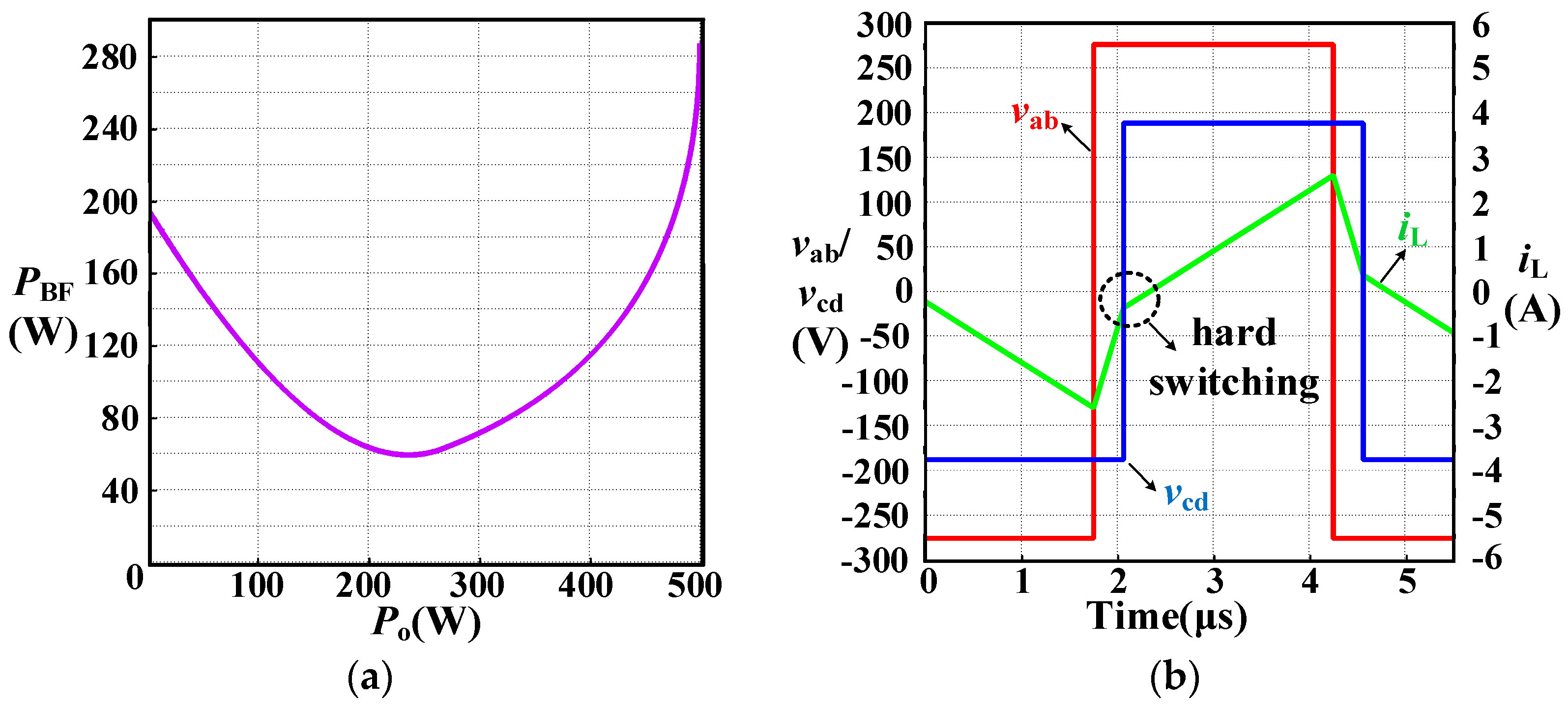
To better illustrate the effectiveness of the proposed method, the SPS modulation method, the DPS-RPS modulation method in [31], and the proposed method are simulated in this paper. In the simulation, the input voltage of the DAB converter is 276 V, the output voltage is 188 V, the inductor Lr is 65 μH, and the rated power PN is 500 W. The simulation results of SPS modulation are shown in Figure 10. Analyzing Figure 10a, it can be obtained that when the DAB is in the buck state and the output power Po is low, the backflow power PBF decreases with the increase in Po because the inductor current iL at the moment of the rising edge of vcd is less than zero. But when the output power Po is larger, the inductor current iL at the moment of the rising edge of vcd crosses the zero point, and the PBF shows a rising trend. From Figure 10a, it can be seen that the backflow power under SPS modulation is larger in the whole power range. And Figure 10b shows the typical waveforms of the SPS modulation method in the low-power range. It demonstrates the difficulty of achieving the ZVS for secondary power switches in the buck state and in the low-power range.
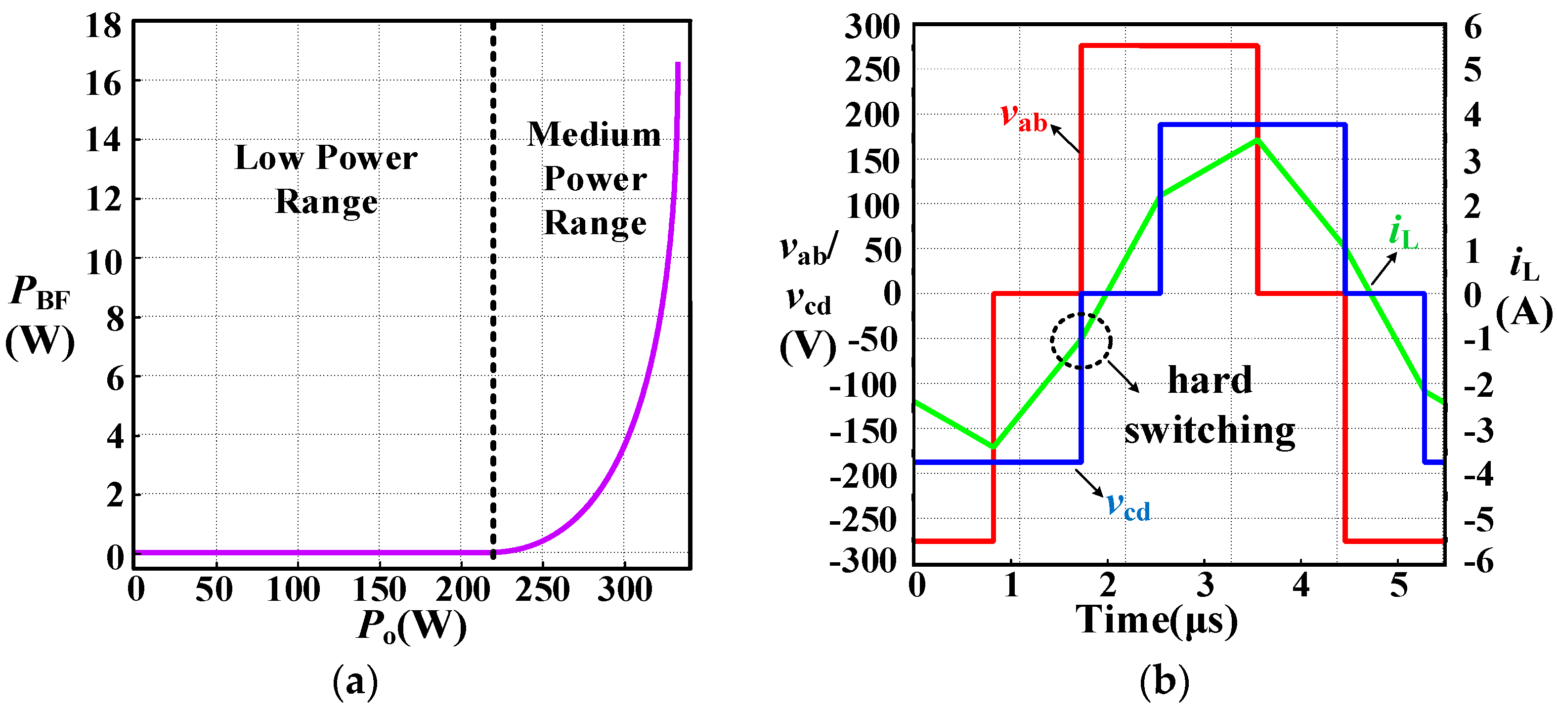
Figure 11a shows the backflow power simulation results of the DPS-RPS modulation method in [31]. Comparing the simulation results shown in Figure 10a, it can be seen that the DPS-RPS modulation method greatly optimizes the dual-side backflow power of DAB in the low- and medium-power range. And the dual-side backflow power of the DAB can even be optimized to zero in the low-power range. Figure 11b shows the typical waveform of the DPS-RPS modulation method in the medium-power range. It can be obtained that the rising edge of vab from zero to positive coincides with the rising edge of vcd from negative to zero, which indicates that there must be a pair of power switches that cannot realize the ZVS in this power range. Although this method optimizes the backflow power, it fails to achieve the collaboration between the minimum backflow power optimization and the realization of ZVS.
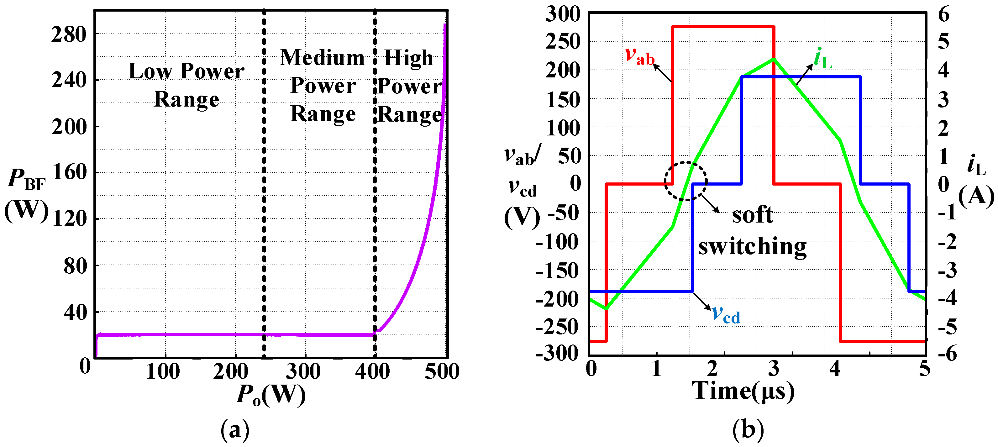
The simulation results of the proposed modulation method are shown in Figure 12. Comparing the simulation results shown in Figure 10a and Figure 11a, it can be seen that the proposed modulation method optimizes the dual-side backflow power of DAB in the full power range. However, the optimization effect of backflow power in the low- and medium-power range is worse than that of the DPS-RPS modulation method in [31]. This is due to the fact that the proposed modulation method opens up a small portion of the necessary backflow power to prioritize the ZVS of the primary and secondary power switches for DAB. Figure 12b shows the typical waveforms of the proposed modulation method in the medium-power range. It can be analyzed that, compared to the simulation results shown in Figure 11b, the phase-shift ratio regulatory factor introduced by the proposed modulation method ensures that a small portion of reverse current flows through the primary and secondary power switches when they are turned on. Although this generates extra backflow power, it ensures the realization of ZVS, which is very favorable for the application of DAB at higher frequencies.

4.2. Experimental Results

To verify the effectiveness of the collaborative modulation method of dual-side backflow power optimization and ZVS for the DAB converter proposed in this paper, a 500W DAB prototype was built, as shown in Figure 13. And the prototype parameters are presented in Table 3. The controller of the prototype adopts the DSP TMS320F28335 from Texas Instruments, Dallas, TX, USA.
Two different voltage gains, k = 0.733 and k = 1.467, are selected in the experiment to validate the proposed modulation method. Since the output capacitance Coss = 45pF of the selected power switches, λ = 0.12 is designed for k = 0.733 and λ = 0.1 for k = 1.467 according to (22). Since the symmetry of the forward and reverse energy flow modulation curves makes the two equivalent to each other, this paper only verifies and analyzes the case of forward power transfer. According to the power interval divided by the optimization modulation curve, in the low-power range, medium-power range, and high-power range, the output power Po is selected separately as 150 W ( P o * = 0.3), 300 W ( P o * = 0.6), and 450 W ( P o * = 0.9) at different voltage gains for the validation analysis of backflow power and the ZVS.
When k = 0.733, the DAB is in the boost state, and its input and output voltages are set experimentally to be 195 V and 266 V. The operation of the DAB at Po = 150 W is shown in Figure 14. In Figure 14 and subsequent waveforms, to facilitate the representation of the backflow power, the region where the backflow power is generated is manually marked with yellow shadow on the acquired experimental waveforms according to the definition of the backflow power in the previous section, as shown by the shadow region of the waveform where the PBF is referred to. And the backflow power PBF under optimization modulation and SPS modulation marked in the experimental waveforms is calculated based on the integration. Taking the waveform shown in Figure 4 as an example, the backflow power calculation method is shown in (23).
P BF = 1 T h s t 1 t c v ab ( t ) i L ( t ) d t + 1 T h s t c t 2 v cd ( t ) i L ( t ) d t
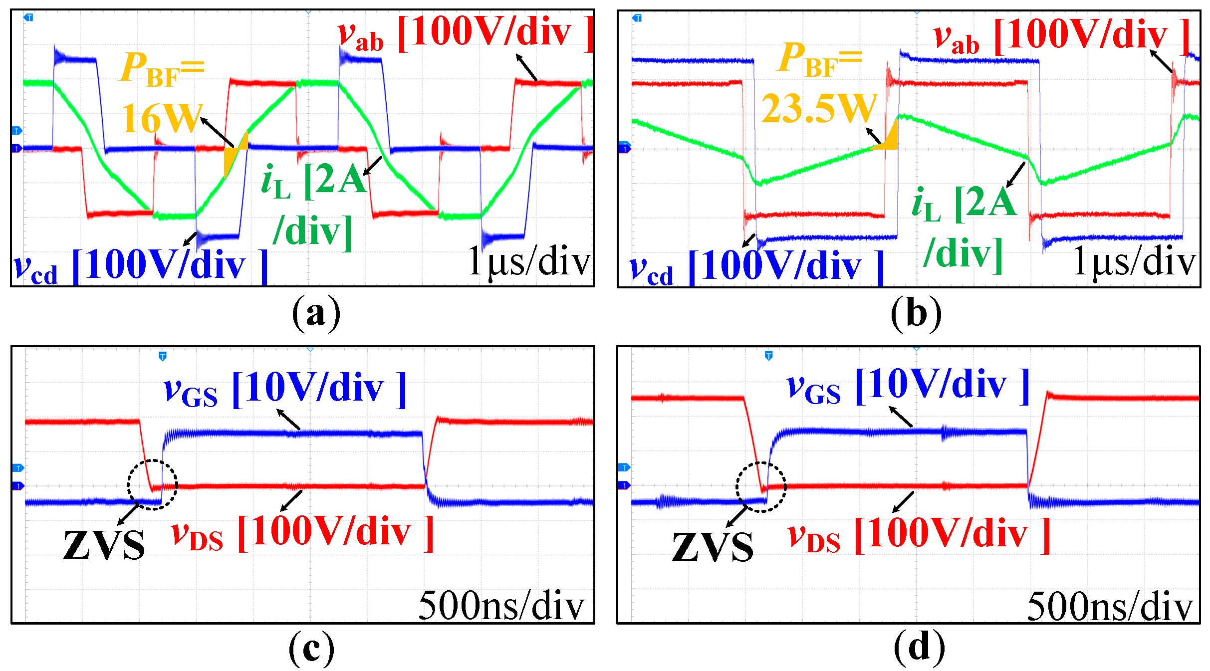
Figure 14 illustrates that the backflow power is reduced in the optimization modulation compared to the SPS modulation. In addition, as shown in Figure 14b, the primary power switch under SPS modulation fails to realize ZVS because the inductor current iL is greater than zero at the turn-on moment. Based on the above analysis of Mode A and Mode B, in the optimization modulation method, as long as Q4P and Q1S can realize ZVS, then all the power switches can realize ZVS. Analyzing Figure 14c,d, both Q4P and Q1S realize ZVS under this condition, and the time between the falling edge of the voltage vDS(t) at the ends of Q1S and the rising edge of the driving voltage vGS(t) is very short, which also indicates that it happens to realize ZVS. In addition, Figure 14a shows that there is always iL > 0 during the time of rising edge of vab(t) from zero to positive, and iL is close to zero when its corresponding Q4P is fully turned on. Also, there is always iL < 0 during the time of the rising edge of vcd(t) from negative to zero, and iL is close to zero when its corresponding Q1S is just turned on. All these show that the optimization modulation method reduces the backflow power to near its minimum value that can be achieved while achieving ZVS in this operation condition.
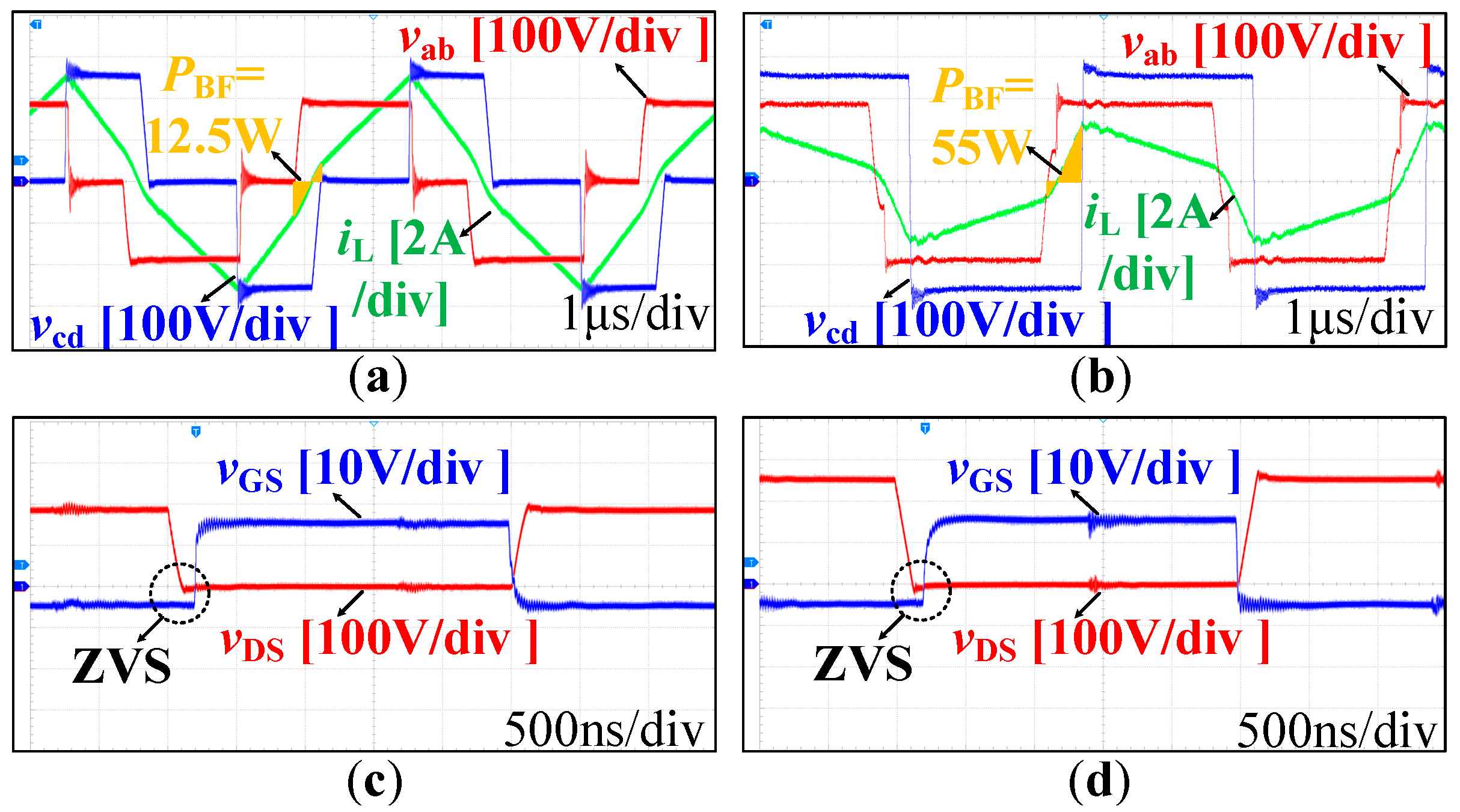
When k = 0.733, as D1 decreases, the DAB operation is shown in Figure 15 when the load power rises to 300W. It can be analyzed that in the medium-power range, although the primary power switch under SPS modulation has a reverse inductor current when it is just turned on, the inductor current iL crosses zero before it is fully turned on. Therefore, it fails to realize ZVS for the whole process. Under the proposed optimization modulation method, Q4P and Q1S realize ZVS with a small ZVS time margin, and the backflow power is reduced to about 1/4 compared with the SPS modulation.
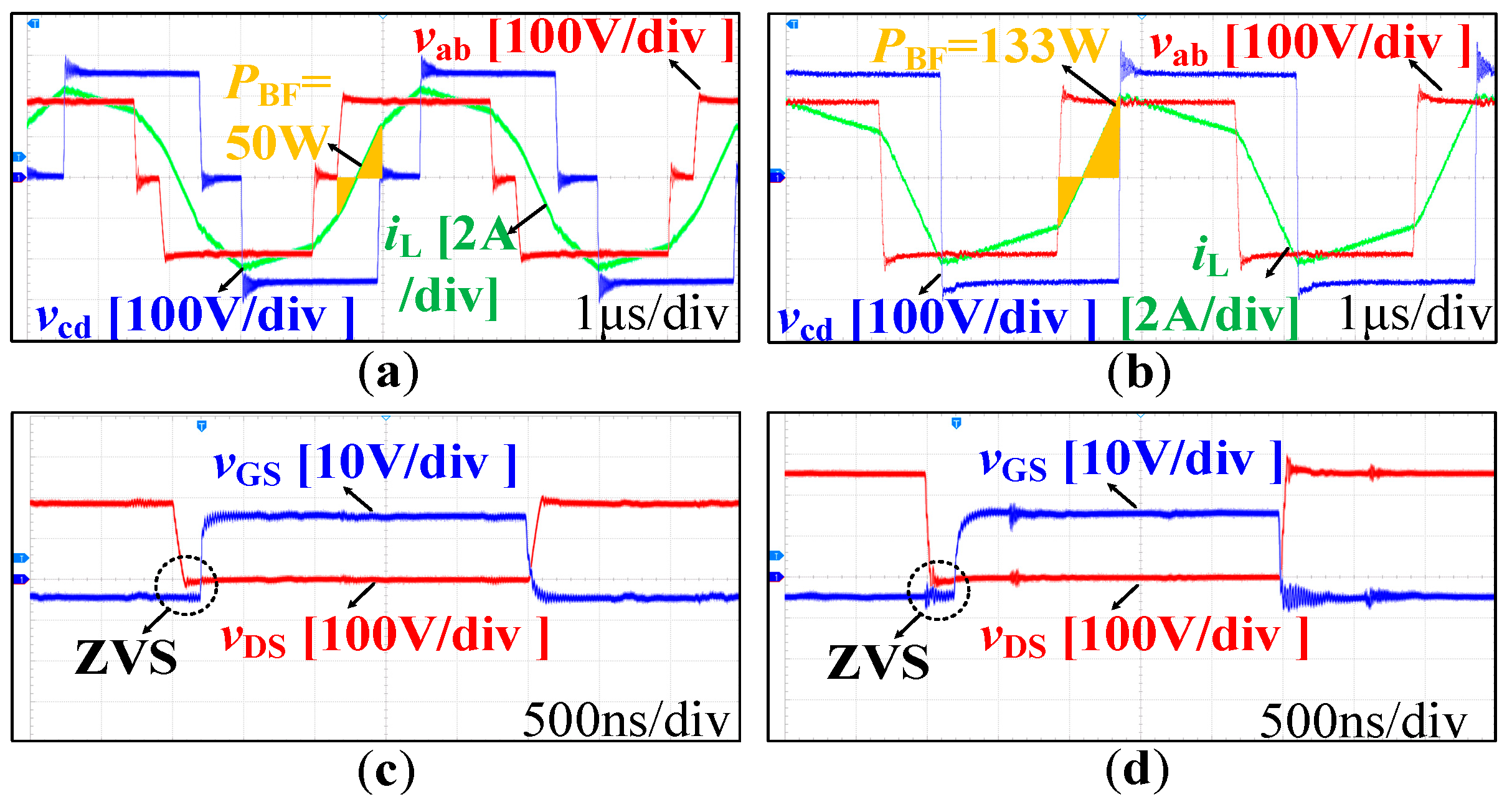
As D1 increases further, when the output power rises to 450 W, the backflow power cannot be regulated to a small value and will increase with the rise in output power. At this stage, either SPS modulation or optimization modulation can achieve ZVS, but optimization modulation can still suppress the backflow power to a certain extent while satisfying the output power, which is consistent with the experimental results shown in Figure 16.
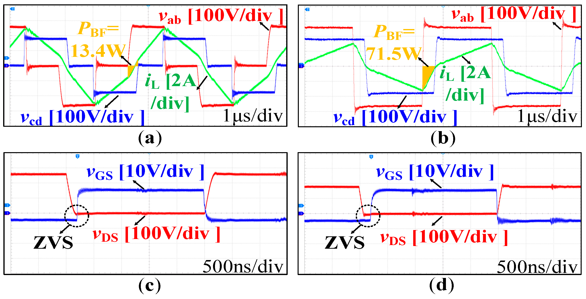
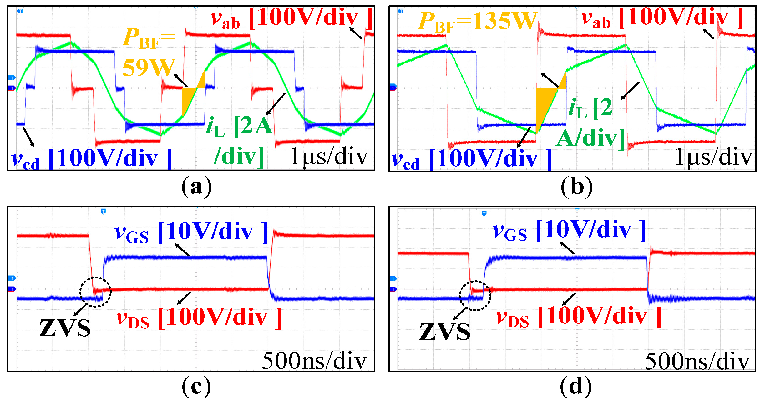
When k = 1.467, the converter is in the buck state, and its input and output voltages are set experimentally to be 265 V and 181 V. The experimental waveforms with an output power of 150W and 300W are shown in Figure 17 and Figure 18. It can be analyzed that the SPS modulation fails to realize the ZVS in both conditions. And in the low-power range, the backflow power is very large, and the converter does not transfer power to the secondary side for about one-third of the half switching cycle. According to the ZVS waveforms of Q4P with optimization modulation under these two conditions, it can be found that Q4P exactly achieves ZVS under the designed λ = 0.12. Meanwhile, the backflow power under optimization modulation is comparable and much smaller than the dual-side backflow power under SPS modulation. This shows that the optimization modulation method proposed in this paper is also feasible in the buck condition and can guarantee the ZVS of the primary and secondary power switches and the optimization of dual-side backflow power at the same time.
From the backflow power magnitude and ZVS condition shown in Figure 19, it can be similarly found that the effect of the optimization modulation method in the condition of buck and high-power range is the same as that in the condition of boost and high-power range. In conclusion, the ZVS of the power switches at three power stages, namely, low power, medium power and high power, under two voltage gains of boost and buck is experimentally investigated, and it is verified that the optimization modulation method proposed in this paper is able to guarantee the realization of the ZVS under a variety of working conditions. Meanwhile, by comparing and analyzing the magnitude of backflow power and the realization degree of the ZVS of power switches, the superiority of the optimization modulation method in suppressing dual-side backflow power is verified, which is consistent with the theoretical design. This demonstrates the feasibility and effectiveness of the proposed dual-side backflow power optimization and ZVS collaboration modulation method of DAB.
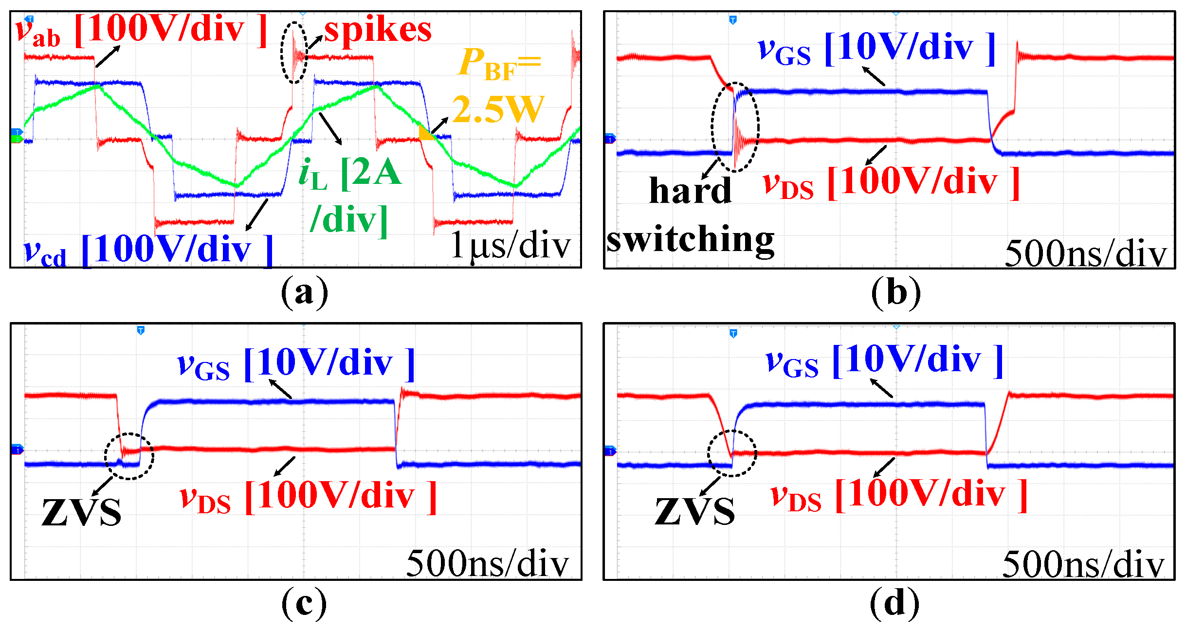
To further elaborate the excellence of the proposed modulation method in the collaboration between backflow power optimization and ZVS of the power switches, the DPS-RPS modulation method in [31] is compared and analyzed in this paper. It provides a simple control interface through the external phase-shift ratio D between the primary and secondary H-bridges. And according to the simulation results shown in Figure 11, it can be seen that the DPS-RPS modulation method only optimizes the backflow power in the low- and medium-power range but not in the high-power range. Therefore, according to the power interval divided by the DPS-RPS modulation method, in the low-power range and medium-power range, the output power Po is selected separately as 150 W ( P o * = 0.3) and 300 W ( P o * = 0.6) for the validation analysis of backflow power and the ZVS. In the experiments, the input and output voltages are set to be 265 V and 181 V. The operation of the DAB under the DPS-RPS modulation method at Po = 150 W is shown in Figure 20. From Figure 20a, it can be seen that the DPS-RPS modulation method optimizes the dual-side backflow power of DAB to a great extent in the low-power range. Compared with the experimental results shown in Figure 17a, it can be obtained that the DPS-RPS modulation method is better than the proposed modulation method in terms of the backflow power optimization in the low-power range, which corresponds to the simulation results. In addition, according to [31], in the DPS-RPS modulation method, as long as Q4P, Q1S, and Q4S can realize ZVS, then all the power switches can realize ZVS. Analyzing Figure 20, Q4P fails to realize ZVS in this case. And in Figure 20a, the voltage spikes appearing at the moment of the rising edge of vab from zero to positive also corroborate the fact that Q4P is in the hard-switching state. The hard switching not only causes EMI but also increases the voltage stress of the power switches. Compared with the experimental results shown in Figure 17, the DPS-RPS modulation method fails to achieve the collaboration between the backflow power optimization and the ZVS implementation in the low-power range. Its excellent effect of backflow power optimization is based on the sacrifice of soft switching.
When the load power rises to 300 W, the DAB operation under DPS-RPS modulation is shown in Figure 21. Compared with the experimental results shown in Figure 18a and Figure 21a, it can be seen that the optimization results of the DPS-RPS modulation method for the backflow power are still very significant in the medium-power range. Meanwhile, the voltage spikes in Figure 21a and the results in Figure 21b indicate that the Q4P fails to realize the complete ZVS. However, it exhibits the trend that the degree of ZVS realization of the Q4P gradually increases with the increase in power. Figure 21d shows that Q4S realizes ZVS exactly in this case, and the trend of the degree of ZVS realization with power is opposite to that of Q4P. Therefore, there must be a pair of power switches that cannot realize the ZVS under DPS-RPS modulation, which echoes the simulation results of the DPS-RPS modulation method. Although the DPS-RPS modulation method has an excellent effect of backflow power suppression in the low- and medium-power range, it is at the expense of the ZVS of the power switches. Also, it cannot optimize the backflow power in the high-power range. In summary, compared with the experimental results of the DPS-RPS modulation method, the modulation method proposed in this paper can not only optimize the backflow power in the full power range but can also collaborate with the ZVS of the power switches. This further illustrates the excellence of the proposed modulation method.

5. Conclusions

To optimize the primary and secondary backflow power of DAB, this paper proposes a collaborative modulation method of dual-side backflow power optimization and ZVS. The modulation method is based on TPS modulation, and two main operation modes are selected for optimization. And according to the degree of backflow power optimization, it is divided into three power intervals to optimize the backflow power separately. The method is not only applicable to different voltage gains but also covers the full load power range. At the same time, the primary H-bridge internal phase-shift ratio is used as the control variable, which provides a simple and feasible modulation interface for the control of the output characteristics. In addition, to address the inherent contradiction between backflow power and the ZVS of the power switches, based on the proposed full-power-range dual-side backflow power optimization modulation method, the collaboration between ZVS and backflow power optimization is achieved over a wide output power range by introducing a phase-shift ratio regulatory factor in the low-power range and medium-power range. And finally, the proposed modulation method achieves the maximum optimization of the backflow power under the premise of guaranteeing the ZVS of the power switches.

Author Contributions

Conceptualization, Y.Z., X.L., and T.L.; methodology, X.L., Z.H., and J.C.; software, X.L.; validation, T.L. and X.L.; formal analysis, Y.Z., X.L., and T.L.; data curation, X.L.; writing—original draft preparation, X.L.; writing—review and editing, Y.Z., Z.H., and J.C.; supervision, Y.Z.; funding acquisition, Y.Z. All authors have read and agreed to the published version of the manuscript.

Funding

This work is supported by the Science and Technology Project of China Southern Power Grid Company [Project Number: 030600KK52222013 (GDKJXM20222579)].

Data Availability Statement

Relevant data are given in this paper.

Conflicts of Interest

Author Jinrong Chen was employed by the Foshan Power Supply Bureau, Guangdong Power Grid Co., Ltd. The remaining authors declare that the research was conducted in the absence of any commercial or financial relationships that could be construed as a potential conflict of interest. The funders had no role in the design of the study; in the collection, analyses, or interpretation of data; in the writing of the manuscript; or in the decision to publish the results.

References

  1. Breyer, C.; Khalili, S.; Bogdanov, D. On the history and future of 100% renewable energy systems research. IEEE Access 2022, 10, 78176–78218. [Google Scholar] [CrossRef]
  2. Dragicevic, T.; Lu, X. DC microgrids—Part I: A review of control strategies and stabilization techniques. IEEE Trans. Power Electron. 2016, 31, 4876–4891. [Google Scholar] [CrossRef]
  3. Chen, Y.; Wang, P. Multicell reconfigurable multi-input multi-output energy router architecture. IEEE Trans. Power Electron. 2020, 35, 13210–13224. [Google Scholar] [CrossRef]
  4. Polat, H.; Hosseinabadi, F.; Hasan, M.M.; Chakraborty, S.; Geury, T.; El Baghdadi, M.; Wilkins, S.; Hegazy, O. A review of DC fast chargers with BESS for electric vehicles: Topology, battery, reliability oriented control and cooling perspectives. Batteries 2023, 9, 121. [Google Scholar] [CrossRef]
  5. Dini, P.; Saponara, S. Modeling and control simulation of power converters in automotive applications. Appl. Sci. 2024, 14, 1227. [Google Scholar] [CrossRef]
  6. Rasool, H.; Verbrugge, B.; Zhaksylyk, A. Design optimization and electro-thermal modeling of an off-board charging system for electric bus applications. IEEE Access 2024, 9, 84501–84519. [Google Scholar] [CrossRef]
  7. Dini, P.; Saponara, S. Electro-thermal model-based design of bidirectional on-board chargers in hybrid and full electric vehicles. Electron. 2022, 11, 112. [Google Scholar] [CrossRef]
  8. Kotb, R.; Chakraborty, S.; Tran, D. Power electronics converters for electric vehicle auxiliaries: State of the art and future trends. Energies 2023, 16, 1753. [Google Scholar] [CrossRef]
  9. Kim, I.; Jang, W.; Kim, M.; Park, J. PFM-PSM hybrid controlled CLLC resonant converter for electric vehicles. In Proceedings of the 2023 IEEE Energy Conversion Congress and Exposition (ECCE), Nashville, TN, USA, 29 October–2 November 2023; pp. 3386–3391. [Google Scholar]
  10. Dini, P.; Saponara, S.; Colicelli, A. Overview on battery charging systems for electric vehicles. Electron. 2023, 12, 4295. [Google Scholar] [CrossRef]
  11. Dini, P.; Ariaudo, G.; Botto, G.; Greca, F.L.; Saponara, S. Real-time electro-thermal modelling and predictive control design of resonant power converter in full electric vehicle applications. IET Power Electron. 2023, 16, 2045–2064. [Google Scholar] [CrossRef]
  12. Chen, X.; Xu, G.; Han, H.; Liu, D.; Sun, Y.; Su, M. Light-load efficiency enhancement of high-frequency dual-active-bridge converter under SPS control. IEEE Trans. Ind. Electron. 2021, 68, 12941–12946. [Google Scholar] [CrossRef]
  13. Xu, G.; Li, L.; Chen, X.; Xiong, W.; Liang, X.; Su, M. Decoupled EPS control utilizing magnetizing current to achieve full load range ZVS for dual active bridge converters. IEEE Trans. Ind. Electron. 2022, 69, 4801–4813. [Google Scholar] [CrossRef]
  14. Li, L.; Xu, G.; Xiong, W.; Liu, D.; Su, M. An optimized DPS control for dual-active-bridge converters to secure full-load-range ZVS with low current stress. IEEE Trans. Transp. Electrific. 2022, 8, 1389–1400. [Google Scholar] [CrossRef]
  15. Huang, J.; Wang, Y.; Li, Z.; Lei, W. Unified triple-phase-shift control to minimize current stress and achieve full soft-switching of isolated bidirectional DC–DC converter. IEEE Trans. Ind. Electron. 2016, 63, 4169–4179. [Google Scholar] [CrossRef]
  16. Liu, P.; Duan, S. A hybrid modulation strategy providing lower inductor current for the DAB converter with the aid of DC blocking capacitors. IEEE Trans. Power Electron. 2020, 35, 4309–4320. [Google Scholar] [CrossRef]
  17. Tian, J.; Wang, F.; Zhuo, F.; Wang, Y.; Wang, H.; Li, Y. A zero-backflow-power EPS scheme with multiobjective coupled-relationship optimization in DAB-based converter. IEEE J. Emerg. Sel. Topics Power Electron. 2022, 10, 4128–4145. [Google Scholar] [CrossRef]
  18. Shi, H.; Wen, H. Minimum-backflow-power scheme of DAB-based solidstate transformer with extended-phase-shift control. IEEE Trans. Ind. Appl. 2018, 54, 3483–3496. [Google Scholar] [CrossRef]
  19. Xu, F.; Liu, J.; Dong, Z. Minimum backflow power and ZVS design for dual-active-bridge DC–DC converters. IEEE Trans. Ind. Electron. 2023, 70, 474–484. [Google Scholar] [CrossRef]
  20. Lin, F.; Zhang, X.; Li, X.; Sun, C.; Cai, W.; Zhang, Z. Automatic triple phase-shift modulation for DAB converter with minimized power loss. IEEE Trans. Ind. Appl. 2022, 58, 3840–3851. [Google Scholar] [CrossRef]
  21. Shao, S.; Jiang, M.; Ye, W.; Li, Y.; Zhang, J.; Sheng, K. Optimal phase-shift control to minimize reactive power for a dual active bridge DC–DC converter. IEEE Trans. Power Electron. 2019, 34, 10193–10205. [Google Scholar] [CrossRef]
  22. Wang, S.; Zheng, Z.; Li, C.; Wang, K.; Li, Y. Time domain analysis of reactive components and optimal modulation for isolated dual active bridge DC/DC converters. IEEE Trans. Power Electron. 2019, 34, 7143–7146. [Google Scholar] [CrossRef]
  23. Li, S.; Yuan, X.; Wang, Z.; Wang, K.; Zhang, Y.; Wu, X. A unified optimal modulation strategy for DAB Converters to tradeoff the backflow power reduction and all ZVS in the full operating range. IEEE J. Emerg. Sel. Topics Power Electron. 2023, 11, 5701–5723. [Google Scholar] [CrossRef]
  24. Jiang, L.; Sun, Y. Integrated optimization of dual-active-bridge DC–DC converter with ZVS for battery charging applications. IEEE J. Emerg. Sel. Topics Power Electron. 2023, 11, 288–300. [Google Scholar] [CrossRef]
  25. Chen, G.; Chen, Z.; Chen, Y.; Feng, C.; Zhu, X. Asymmetric phase-shift modulation strategy of DAB converters for improved light-load efficiency. IEEE Trans. Power Electron. 2022, 37, 9104–9113. [Google Scholar] [CrossRef]
  26. Xie, F.; Wang, H.; Shu, J. Backflow power optimization of DAB based on asymmetric duty cycle and internal phase shift control. IEEE Access 2023, 11, 25682–25688. [Google Scholar] [CrossRef]
  27. Chen, G.; Chen, Z.; Chen, Y.; Feng, C.; Zhu, X. Comprehensive analysis of asymmetric modulated dual-active-bridge converter and its hybrid control strategy. IEEE J. Emerg. Sel. Topics Power Electron. 2022, 10, 4218–4230. [Google Scholar] [CrossRef]
  28. Gu, Q.; Yuan, L.; Nie, J.; Sun, J.; Zhao, Z. Current stress minimization of dual-active-bridge DC–DC converter within the whole operating range. IEEE J. Emerg. Sel. Topics Power Electron. 2019, 7, 129–142. [Google Scholar] [CrossRef]
  29. Lai, J.; Yao, X.; Su, J. Improved CTPS control for dual active bridge DC-DC converter under dead time influence. High Voltage Eng. 2023, 49, 4827–4838. [Google Scholar]
  30. Xiong, F.; Wu, J.; Hao, L. Backflow power optimization control for dual active bridge DC-DC converters. Energies 2017, 10, 1403. [Google Scholar] [CrossRef]
  31. Li, S.; Wang, H.; Ye, W.; Fang, Q.; Yan, P. Dual phase shift modulation strategy for reactive power suppression of a DAB converter. Power Syst. Prot. Control 2022, 50, 14–23. [Google Scholar]
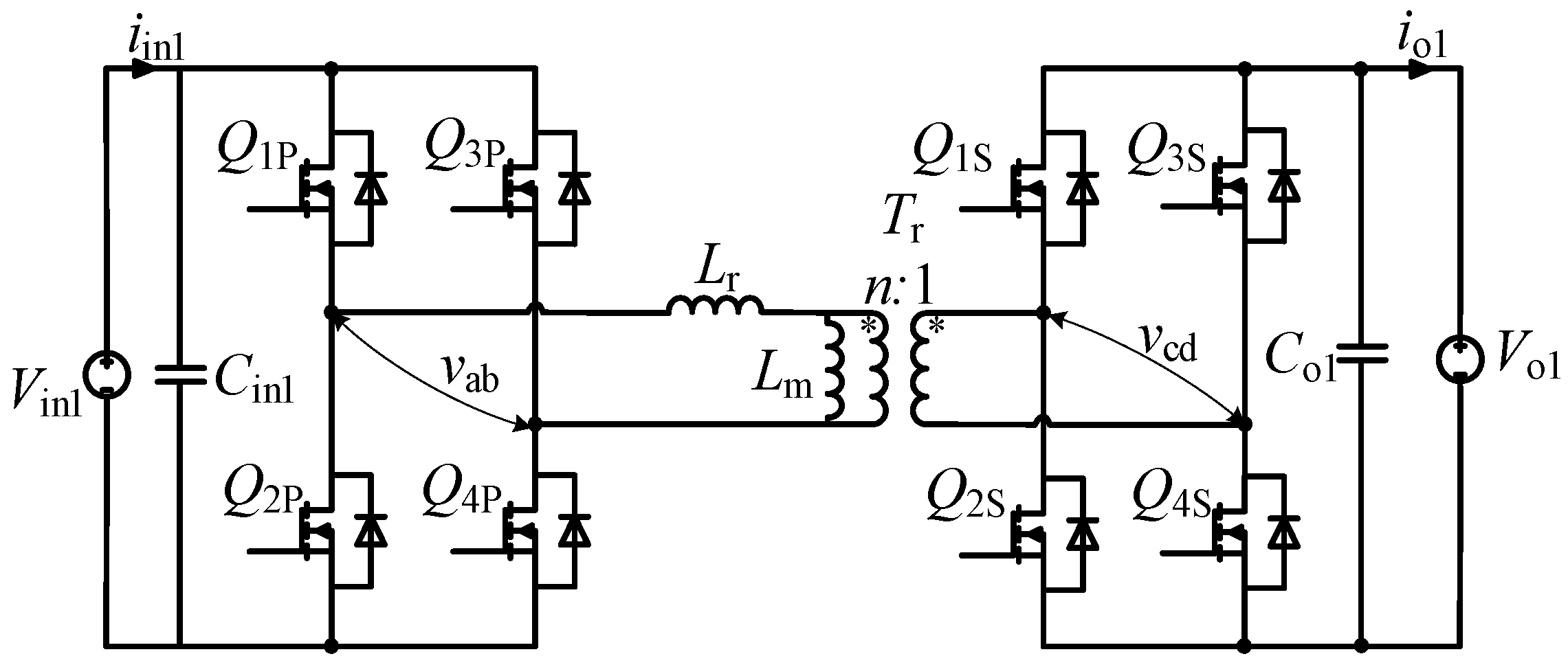
Figure 1. Topology of a typical DAB converter.
Energies 17 03019 g001
Figure 2. Waveforms of the driving signals with TPS.
Energies 17 03019 g002
Figure 3. The operation modes of TPS modulation: (a) Mode A; (b) Mode B; (c) Mode C; (d) Mode D; (e) Mode E; (f) Mode F; (g) Mode G; (h) Mode H; (i) Mode I; (j) Mode J; (k) Mode K; (l) Mode L.
Energies 17 03019 g003
Figure 4. Waveforms of inductor current and H-bridge midpoint voltages in Mode A.
Energies 17 03019 g004
Figure 5. Waveforms of inductor current and H-bridge midpoint voltages in Mode B.
Energies 17 03019 g005
Figure 6. Relationship diagrams under optimization modulation method: (a) diagram of P o * versus D1; (b) diagram of P BF * versus D1.
Energies 17 03019 g006
Figure 7. Diagram of backflow power in full power range.
Energies 17 03019 g007
Figure 8. Operation range of optimization modulation method for different voltage gains: (a) operation range of D1; (b) operation range of P o * .
Energies 17 03019 g008
Figure 9. Control structure diagram of backflow power optimization modulation method based on ZVS collaboration.
Energies 17 03019 g009
Figure 10. Simulation results of SPS modulation method: (a) diagram of PBF versus Po; (b) waveforms of vab, vcd, and iL in one switching period.
Energies 17 03019 g010
Figure 11. Simulation results of DPS-RPS modulation method in [31]: (a) diagram of PBF versus Po; (b) waveforms of vab, vcd, and iL in one switching period.
Energies 17 03019 g011
Figure 12. Simulation results of the proposed collaborative modulation method: (a) diagram of PBF versus Po; (b) waveforms of vab, vcd, and iL in one switching period.
Energies 17 03019 g012
Figure 13. Experimental prototype.
Energies 17 03019 g013
Figure 14. Waveforms for k = 0.733 and Po = 150 W: (a) backflow power with optimization modulation; (b) backflow power with SPS modulation; (c) ZVS of Q4P; (d) ZVS of Q1S.
Energies 17 03019 g014
Figure 15. Waveforms for k = 0.733 and Po = 300 W: (a) backflow power with optimization modulation; (b) backflow power with SPS modulation; (c) ZVS of Q4P; (d) ZVS of Q1S.
Energies 17 03019 g015
Figure 16. Waveforms for k = 0.733 and Po = 450 W: (a) backflow power with optimization modulation; (b) backflow power with SPS modulation; (c) ZVS of Q4P; (d) ZVS of Q1S.
Energies 17 03019 g016
Figure 17. Waveforms for k = 1.467 and Po = 150 W: (a) backflow power with optimization modulation; (b) backflow power with SPS modulation; (c) ZVS of Q4P; (d) ZVS of Q1S.
Energies 17 03019 g017
Figure 18. Waveforms for k = 1.467 and Po = 300 W: (a) backflow power with optimization modulation; (b) backflow power with SPS modulation; (c) ZVS of Q4P; (d) ZVS of Q1S.
Energies 17 03019 g018
Figure 19. Waveforms for k = 1.467 and Po = 450 W: (a) backflow power with optimization modulation; (b) backflow power with SPS modulation; (c) ZVS of Q4P; (d) ZVS of Q1S.
Energies 17 03019 g019
Figure 20. Waveforms for DPS-RPS modulation method at Po = 150 W: (a) backflow power with DPS-RPS modulation; (b) ZVS of Q4P; (c) ZVS of Q1S; (d) ZVS of Q4S.
Energies 17 03019 g020
Figure 21. Waveforms for DPS-RPS modulation method at Po = 300 W: (a) backflow power with DPS-RPS modulation; (b) ZVS of Q4P; (c) ZVS of Q1S; (d) ZVS of Q4S.
Energies 17 03019 g021
Table 1. Backflow power optimization results.
Low-Power RangeMedium-Power RangeHigh-Power Range
Range of D1[1 − 1/(k + 1), 1][k2/(k2 + k + 1), 1 − 1/(k + 1)][0, k2/(k2 + k + 1)]
DD1D1(1 + ((k2k − 1)D1)/k2)/2
D21 − k + kD11 − k + kD1D1/k2
P BF * 00[0, (k3 + 1)/(2k2 + 2k)]
Range of P o * [0, 2k/(k + 1)2][2k/(k + 1)2, 2k/(k2 + k + 1)][2k/(k2 + k + 1), 1]
Table 2. Comparison of backflow power optimization modulation methods for DAB.
Comparison CategoryBackflow Power OptimizationFull-Power-Range OptimizationCollaboration with ZVSSimple Control InterfaceContinuity of Results Unity under Different Voltage Gains
PrimarySecondary
SPSNoNo//YesYesYes
Optimal algorithm in [19]YesNoYesYesNoNoNo
ICTPS
in [29]
YesYesNoNoNoNoNo
GMPBC
in [30]
YesYesYesNoNoNoYes
DPS-RPS
in [31]
YesYesNoNoYesYesNo
Proposed methodYesYesYesYesYesYesYes
Table 3. Prototype parameters.
ParameterValue
Input voltage Vin1195–265 V
Output voltage Vo1181–266 V
Output current io12.76 A@181 V, 1.9 A@265 V
Output ripple current irp500 mA
Transformer magnetic inductance Lm210 μH
Transformer turns ratio n1:1
Leakage inductance Lr60.5 μH
Switching frequency fs200 kHz
Power switch dead time tdead100 ns
Rated power PN500 W
Power switchesC3M0120065K
Power switch output capacitors Coss45 pF
Disclaimer/Publisher’s Note: The statements, opinions and data contained in all publications are solely those of the individual author(s) and contributor(s) and not of MDPI and/or the editor(s). MDPI and/or the editor(s) disclaim responsibility for any injury to people or property resulting from any ideas, methods, instructions or products referred to in the content.