Article

A Novel Non-Isolated Bidirectional DC-DC Converter with Improved Current Ripples for Low-Voltage On-Board Charging

by
Jamil Muhammad Khan
,
Ashraf Ali Khan
* and
Mohsin Jamil
Faculty of Engineering and Applied Science, Memorial University of Newfoundland, St. John’s, NL A1B 3X5, Canada
*
Author to whom correspondence should be addressed.
Energies 2024, 17(14), 3570; https://doi.org/10.3390/en17143570 (registering DOI)
Submission received: 13 June 2024 / Revised: 10 July 2024 / Accepted: 15 July 2024 / Published: 20 July 2024

Abstract

:
This paper presents a novel single-phase non-isolated bidirectional buck converter topology. The proposed converter uses a basic switching cell structure with a coupled inductor and an interleaving switching scheme. This article addresses a crucial challenge in bidirectional DC-DC conversion by prioritizing reducing output current ripples and minimizing filter inductor size. The employed method includes using MOSFETs with fast recovery diodes to mitigate reverse recovery and body diode losses. Furthermore, the optimization of the switching frequency of the output inductor to be twice the actual switching frequency contributes to reducing the component size of the converter. The coupled inductor also helps to reduce stress on components by distributing currents among its legs. The experimental result demonstrates the proposed converter has a very low ripple current as compared to the conventional converter. The low current ripples and smaller filter inductor size enabled by high-frequency operation have improved the efficiency and size of the converter. A common ground between input and output terminals ensures robust performance without common mode current concerns. Overall, the proposed converter represents a significant improvement in DC-DC converters, promising enhanced efficiency, reliability, and compactness in bidirectional DC-DC conversion systems. In order to verify the performance of the proposed converter, a 460 W buck converter prototype was built and tested.

1. Introduction

The rise in fossil fuel usage has led to significantly increased greenhouse gas emissions, which are the primary cause of global warming. Therefore, sourcing the world’s energy needs from clean and renewable energy sources is inevitable. These renewable sources are environmentally sustainable and align with the 2030 Sustainable Development Goals (SDGs) [1].
Renewable energy sources such as photovoltaics, wind power generation, and fuel cells provide a stable voltage to a DC bus through DC-DC converters [2]. These DC-DC converters are further used to charge batteries. DC-DC converters can be categorized into unidirectional and bidirectional. Unidirectional converters allow the flow of current only in one direction, while bidirectional converters allow current flow in both directions, enabling the use of a single converter for both energy transfer and storage applications [3].
Bidirectional DC-DC converters (BDCs) play a pivotal role across various applications such as aerospace power systems, energy storage systems (ESS) in DC micro-grids [4], and electric vehicles (EVs). As already discussed in the existing literature [4,5], BDCs store generated energy in batteries, and in time of need, these converters enable energy transfer from batteries to load. The bidirectional operation of these converters is essential, allowing them to transfer energy in both directions while ensuring voltage stability and efficiency. Moreover, bidirectional converters are integral to electric drive systems, particularly in electric transportation [6], where they fulfill the dual function of stepping up voltage during power delivery from the source to the motor and stepping down voltage during regenerative braking.
Bidirectional DC-DC converters (BDCs) can be further classified into isolated and non-isolated converters. Isolated converters have electrical isolation for safety, but they can be bulky and costly due to the use of transformers, and they also suffer from high leakage inductance [7]. Non-isolated converters lack galvanic isolation but offer higher efficiency, compact size, and lower cost, making them preferable in many applications [8]. The conventional non-isolated buck/boost bidirectional DC-DC converters are famous for their simple structure and affordability. However, circuit parasitic parameters and the requirement for an extreme duty ratio limit its maximum achievable voltage gain. Additionally, the converter experiences high-voltage stress [7]. These converters also encounter a common issue of high ripple current on the low-voltage (LV) side. This causes the performance of BDC applications involving ESS as the large ripple current negatively impacts battery performance and lifespan [9].
Several conversion techniques are used in BDCs, including multilevel techniques [8,10], cascaded techniques [11,12], voltage multiplier [13], switched-inductor, switched-capacitor [14,15], and coupled-inductor [2,12,16,17].
The multilevel technique improves the voltage conversion ratio and reduces voltage stresses on power switches. However, this method increases the number of switches and the control complexity. Cascaded structures reduce the high-voltage stresses on power switches but result in a lower power density and increased converter cost. Similarly, a switch inductor can lead to low switch stress and high gain, but the difference between the low-voltage side (LVS) and high-voltage side (HVS) can lead to EMI problems [14]. The couple-inductor topologies can increase the gain, but the leakage inductance issue can produce high-voltage spikes on switches and may require additional snubber circuitry [16].
One common issue in the above-mentioned BDCs is the presence of a significant ripple current on the LVS. This ripple current is a problem for battery energy storage systems (BESSs), which are sensitive to such fluctuations. Excessive ripple currents can shorten the lifespan of the BESS [18,19]. To minimize current ripples in converters, several techniques can be used as discussed below:
  • One approach is to increase the inductance of the inductors. This reduces the current ripple, but it can slow down the dynamic response, cost, and size of the converter due to the larger inductor size [20].
  • Using a large capacitor can solve the ripple issues, but it increases the size and cost of the converter.
  • Increasing the switching frequency can help reduce ripple current and allow for smaller inductors. However, the switching frequency increase is constrained by gate drive circuit limitations, switching losses, and electromagnetic compliance requirements.
  • Implementing DCM in converters can lower inductor size. However, the higher inductor current in DCM mode increases switch stress, leading to increased power loss.
  • The inductor ripple can be reduced by employing the interleaving technique [21]. Although effective, this method increases the number of switches and inductors, thereby complicating control and increasing the converter cost.
  • Utilizing cascaded converters with phase shifts can also decrease inductor ripples [19]. However, this approach may raise the complexity and cost due to an increase in the component count. The converter must also operate within a fixed duty cycle.
Each technique for reducing the ripple current in bidirectional DC-DC converters involves trade-offs in performance, complexity, and cost. The choice depends on specific design requirements and constraints. Recent advancements in interleaving DC-DC converters have made them an excellent choice for increased power density and higher efficiency; for example, the authors of [22] discussed the design and modeling of a DC-DC converter using an interleaving technique, and by exploiting the quasi-saturated inductor, the authors reduced the size of the inductor. Similarly, in [23], a more robust nonlinear control technique was devised for an interleaved converter against parameter variations.
While previous studies have examined various non-isolated bidirectional converters, few have focused on using a coupled inductor in a non-isolated DC-DC converter, as shown in our design (Figure 1). This concept, however, has been applied in DC-AC converters [24,25], as well as in AC-AC applications [26]. This observation highlights the versatility and widespread applicability of the mentioned coupled inductor with cell structure topology across various domains within power electronics.
This study addresses the challenge of optimizing voltage reduction while maintaining efficiency and compactness in bidirectional buck converters. We propose a novel design for onboard charging and battery energy storage systems (BESSs), employing coupled inductors and an interleaved PWM scheme for improved efficiency, reduced size, and simplified control. The proposed non-isolated BDC has the following main characteristics:
  • Low-output ripple current;
  • The inductor operates at twice the switching frequency;
  • Reduced inductor size;
  • Low-voltage stresses on power switches;
  • Common ground between LVS and HVS;
  • No additional RC snubber circuit is required;
  • No shoot-through or dead time issue;
  • Less component count and reduced overall size.
The subsequent sections of this paper delve into the proposed buck converter topology, proposed switching (Section 2), modes of operation (Section 3), ripple current analysis and component selection (Section 4), stress and power loss analysis (Section 5), experimental results (Section 6), and discussion and conclusion in the last section.

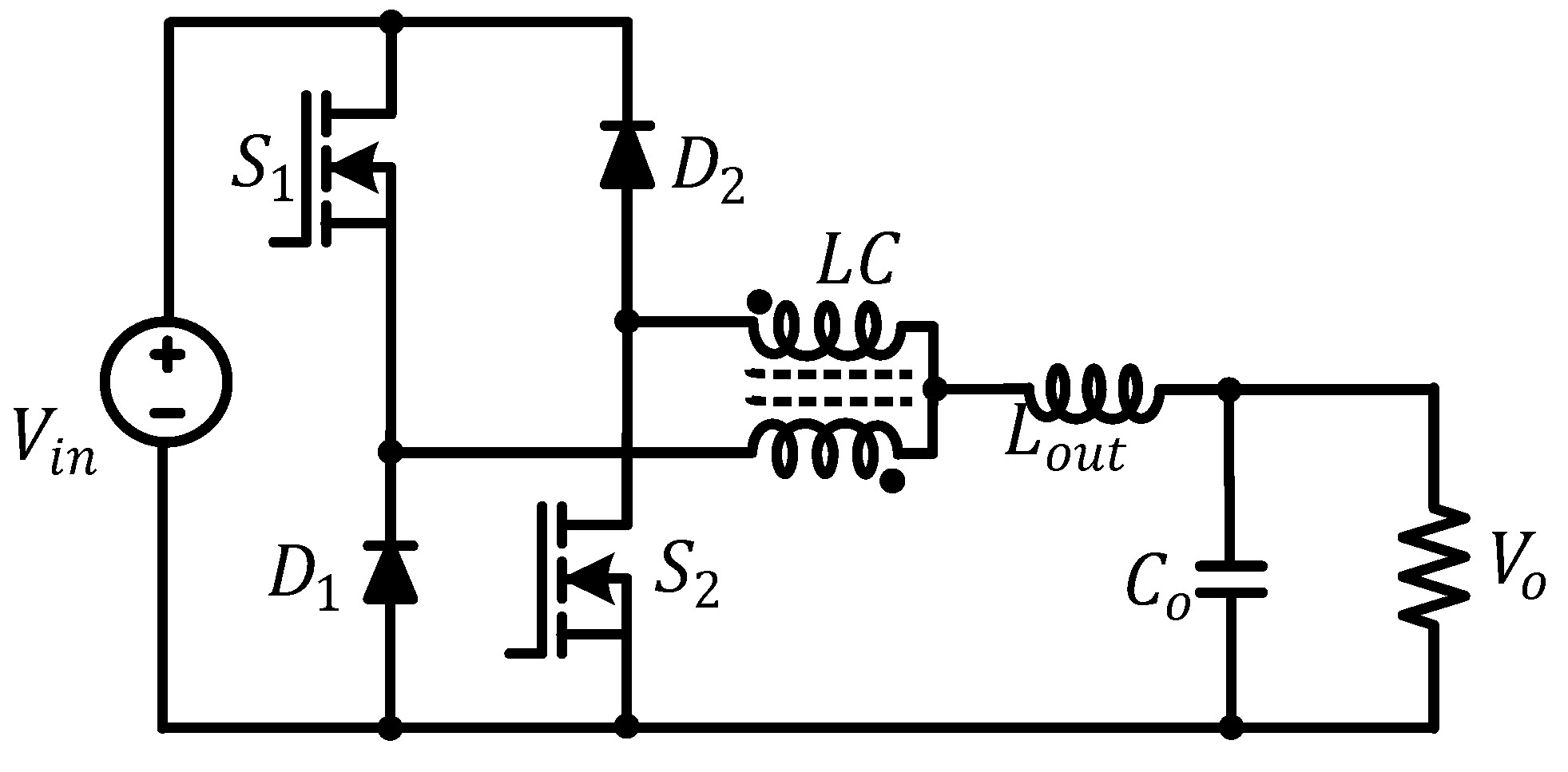
2. Proposed Buck Converter Topology and Switching Scheme

2.1. Proposed Topology

The proposed circuit of a non-isolated bidirectional buck DC-DC converter is shown in Figure 1. This converter employs two active switches (S1, S2) and two independent diodes (D1, D2), a coupled inductor (CL) which is specifically chosen with a coupling factor of k = 1, an output filter inductor (Lout) and capacitor (Co). The input source voltage is denoted by Vin, and Vo represents the output voltage. The switches operate at a switching frequency of 50 kHz. This circuit configuration offers several benefits. This converter demonstrates reduced output filter inductor (Lout) requirements as it experiences double switching frequency and low-voltage stress. Additionally, by utilizing a fundamental switching cell structure, the proposed circuit eliminates the shoot-through and dead-time concerns. Moreover, the circuit features a shared ground, making it well-suited for applications in renewable energies.

2.2. Proposed Switching Scheme

The proposed modulating signals designed for driving the switches are shown in Figure 2. The suggested converter employs an interleaved PWM switching scheme depicted in Figure 2. The switching signals are generated by comparing a DC reference voltage with two 50 kHz triangular waves (Vtri1, Vtri2), which are out of phase by 180 degrees. The output signal for triangular wave (Vtri1) is fed to a NOT gate to operate Switch S1. This configuration encompasses both dead time and overlap time operation modes. The duty cycle, as denoted by D, signifies the duration during which S1 is in the “ON” state within a single switching period (Ts).

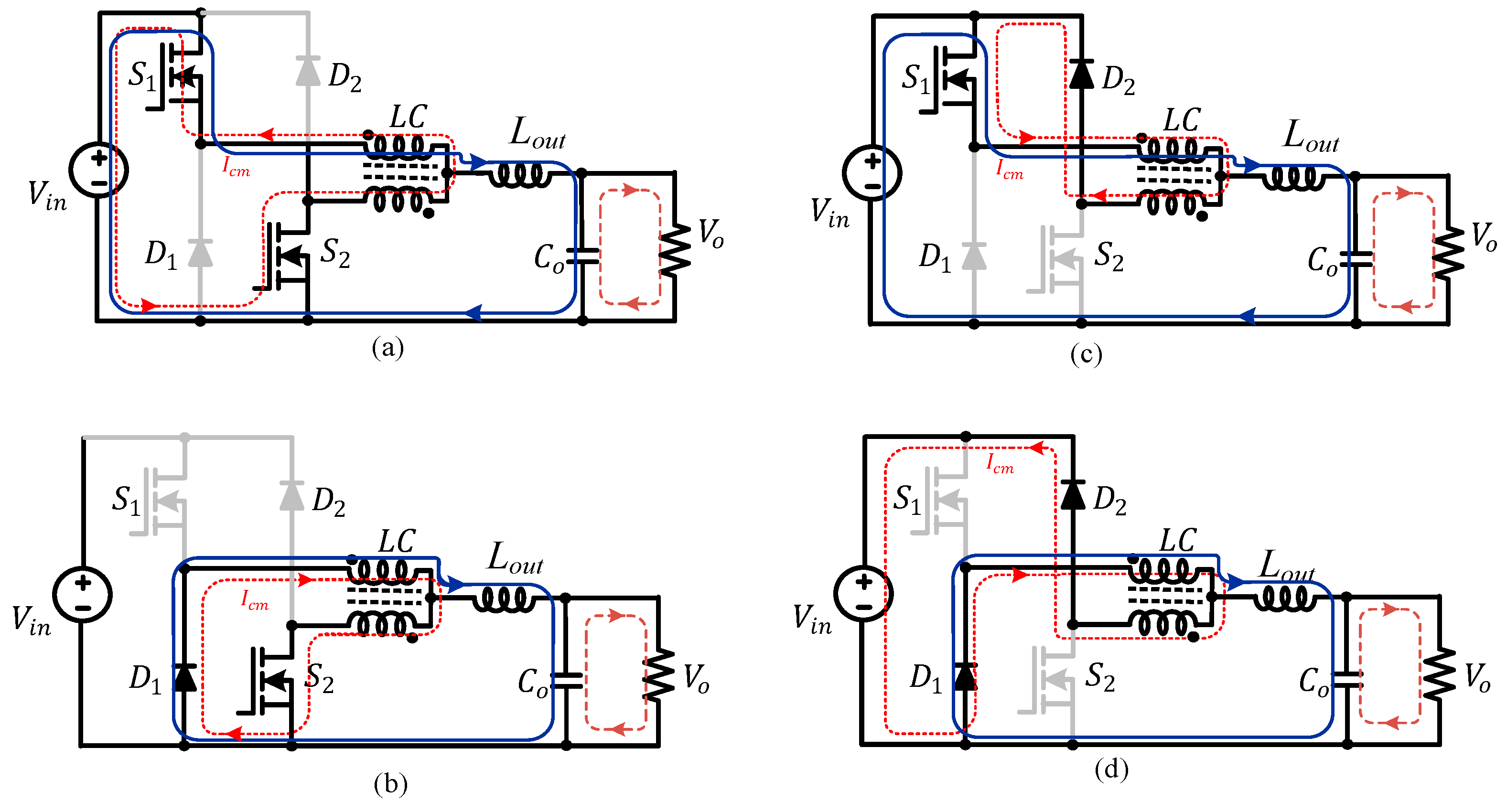
3. Modes of Operation

The suggested converter operates in four different modes as shown in Figure 3. The green bold path in the Figure 3 indicate the current path, the dotted line indicate the common mode current (Icm), the brown doted path indicate the output capacitor current. The system comprises two current components: the output inductor current (Iout); the common mode current (Icm), often referred to as circulating current as shown in Figure 4. In this topology, it is assumed that the coupled inductors are identical, and the coupling coefficient, K, is deliberately set to 1, signifying tight coupling. The operation modes are discussed below for a duty ratio greater and less than zero (D < 0, D > 0). The key simulation waveforms are shown in Figure 5a,b for each duty ration (D < 0, D > 0). The green color triangular wave (Vtr1) and the dotted colored triangular signal (Vtr2), which are 180 degree out of phase are compared with a reference voltage indicated by the red line (Vref). The corresponding switching signal (S1) is generated when the reference voltage is greater than (Vtr1), similarlry, switching signal (S2) is generated when the reference voltage (Vref) is less than (Vtr2).

3.1. Operation Mode for D < 0

Mode 1: Mode 1 is shown in Figure 3a. During this mode, switches S1 and S2 are both turned ON, and the diodes D1, and D2 are reverse-biased. The output inductor (Lout) is charged in this mode, and the filter capacitor Co supplies the output voltage. The voltage and current equations are as follows:
For tight coupling, k = 1 and   V C o = V o , and we obtain
V L o u t = V i n 2 V o
L o u t d I L o u t d t = V i n 2 V o
Similarly, the voltage across the coupled inductor is given by
V L o u t = L d I i n d t
where L is the inductance of L 1 and L 2 .
Mode 2: During this interval, the switch S1 is turned OFF, and S2 is ON; the diode D1 is conducting the circulating current due to freewheeling action, and D2 remains OFF. Mode 2 is shown in Figure 3b. The voltage and current equations are as follows:
V L o u t = V o
L o u t d I L o u t d t = V o
Mode 3: During this interval, S1 and S2 are turned off, and diodes D1 and D2 are conducting as shown in Figure 3d. The voltage and current equation are as follows
V L o u t = V i n 2 V o
L o u t d I L o u t d t = V i n 2 V o
Mode 4: Mode IV is shown in Figure 3b. It is same as Mode II.

3.2. Operation Modes for D > 0

Mode 1: As shown in Figure 3a, Mode I is the same for both D < 0 and D > 0.
Mode 2: During this interval, the switch S1 is turned ON and S2 is OFF, the diode D2 is conducting the circulating current due to freewheeling action, and D1 remains OFF. From Figure 3c the equations for voltage and current are the same as Equations (6) and (7)
Mode 3: During this mode, S1 and S2 are turned off and diodes D1 and D2 are conducting as shown in Figure 3d. Mode III is same for both D > 0 and D < 0.
Mode 4: Mode IV is the same as Mode II, as indicated in Figure 3c.
The output voltage gain of the proposed buck converter can be obtained by applying the Volt-Sec balance condition on L o u t , which leads to the following equation:
V o = D V i n
Equation (8) is the ideal gain equation of the proposed converter. This equation is similar to a conventional buck converter
The non-ideal model of the proposed converter is shown in the Figure 6. To derive the non-ideal gain equation, different non-idealities such as equivalent series resistance (ESR) of inductor   r l a , ESR of capacitor r c , switch on-resistance r s w , diode forward resistance r D , Coupled inductor equivalent series resistance   r L a , and diode forward voltage drop V F are considered. The values of these parasitic resistances are very small in comparison to load resistance R.
Since, a negligible current is passing through inductor of the coupled inductor L b , the ESR of this branch is therefore not considered. The non-ideal gain equation is given by Equation (9)
V o u t = V i n D 2 D 1 + r s w   +   r l a   +   r L o u t R + 2 ( 0.5 D ) ( 1 + r L o u t R )

4. Ripple Current Analysis and Component Selection

In this section, the current ripple magnitudes of the input and coupled inductors are discussed.

4.1. Inductor Design

From Equations (7) and (8), the input inductor equation can be derived as
L o u t d I L o u t d t = ( V i n 2 V o u t ) 2
From Equation (6)
L o u t ( V i n 2 V i n D ) D T s 2 Δ I L o u t V i n D 2 D 2 2 I f s w
I = x % I o u t , with x% denoting the maximum permissible current ripple (10–20%) for the inductors and T s = 1 f s is the switching period of the converter
L o u t V i n · D 1 2 D x % I L o u t f s
Assuming that the ripple inductor current ripple I L o u t is equal to the output ripple current I o u t , since the capacitor draws a negligible current. The output inductance equation L o u t can be derived using (10) as
L o u t V i n D 1 2 D x % I o u t f s
The inductor equation can be written in terms of the input voltage by assuming that the converter is lossless; i.e., P o u t = P i n . Equation (11) becomes
L o u t V i n 2 D 2 1 2 D x % P o u t f s

4.2. Output Inductor Ripple

The current ripple Δ I L o u t through the filter inductor L o u t can be calculated from (11)
Δ I L o u t = V i n D 1 2 D L o u t f s
From Equation (13), maximum ripples in the inductor current occur at D = 0.25 and T s = 1 f s is the switching period of the converter.

4.3. Comparison of Current Ripples

The ripple current for the conventional converter can be derived as
Δ I c o n v = ( V i n V o ) D T s L c o n v  
Using (15) and (16), the ratio of conventional versus proposed induction ripple current ( Δ I c o n v / Δ I L p r o p ) can be written as
Δ I c o n v Δ I L o u t = 1 D 1 2 D
Figure 7 illustrates the current ripple ratio with variations in the duty ratio (D) from 0 to 0.5. As depicted, the ripple current for the conventional buck converter ( Δ L c o n v ) is notably larger compared to that of the proposed converter ( L i n c o n v ) . For example, when D = 0.47, ( Δ I c o n v ) is nearly 10 times greater than the current ripples of the proposed converter ( Δ I L o u t ). The graph clearly illustrates that the proposed converter offers a very low ripple current, making it suitable for charging energy storage elements without affecting their health.

4.4. Couple Inductor Design

The coupled inductance using common mode current from Equation (3) can be written as
d I c m d t = V i n 4 L s d I c m = d t V i n 4 L s
L s = V i n × D T s 4 d I c m  
where L s is self-inductance of the coupled inductor.
L s = L K + L m
The leakage inductance is considered very small ( L K   0 ), and Equation (20) becomes
L s = L m
Equation (19) can be written as
L m = V i n × D T s 4 d I c m

4.5. Output Inductor Comparison

Using Equations (15) and (16), the normalized ratio of the conventional versus proposed output inductance ( L c o n v L p r o p ) can be derived as below.
L c o n v L p r o p = 1 D 1 2 D
Figure 8 illustrates the necessary inductance value for the conventional DC-DC converter for the same current ripple value as observed in the proposed converter, with variations in duty ratio (D) from 0 to 0.5. As depicted, the output inductance for the conventional DC-DC converters ( L o u t . c o n v ) is notably larger than that of the proposed converter ( L o u t . p r o p ) . For example, when D = 0.47, L o u t . c o n v is nearly 13.5 times the size of the proposed output inductor.

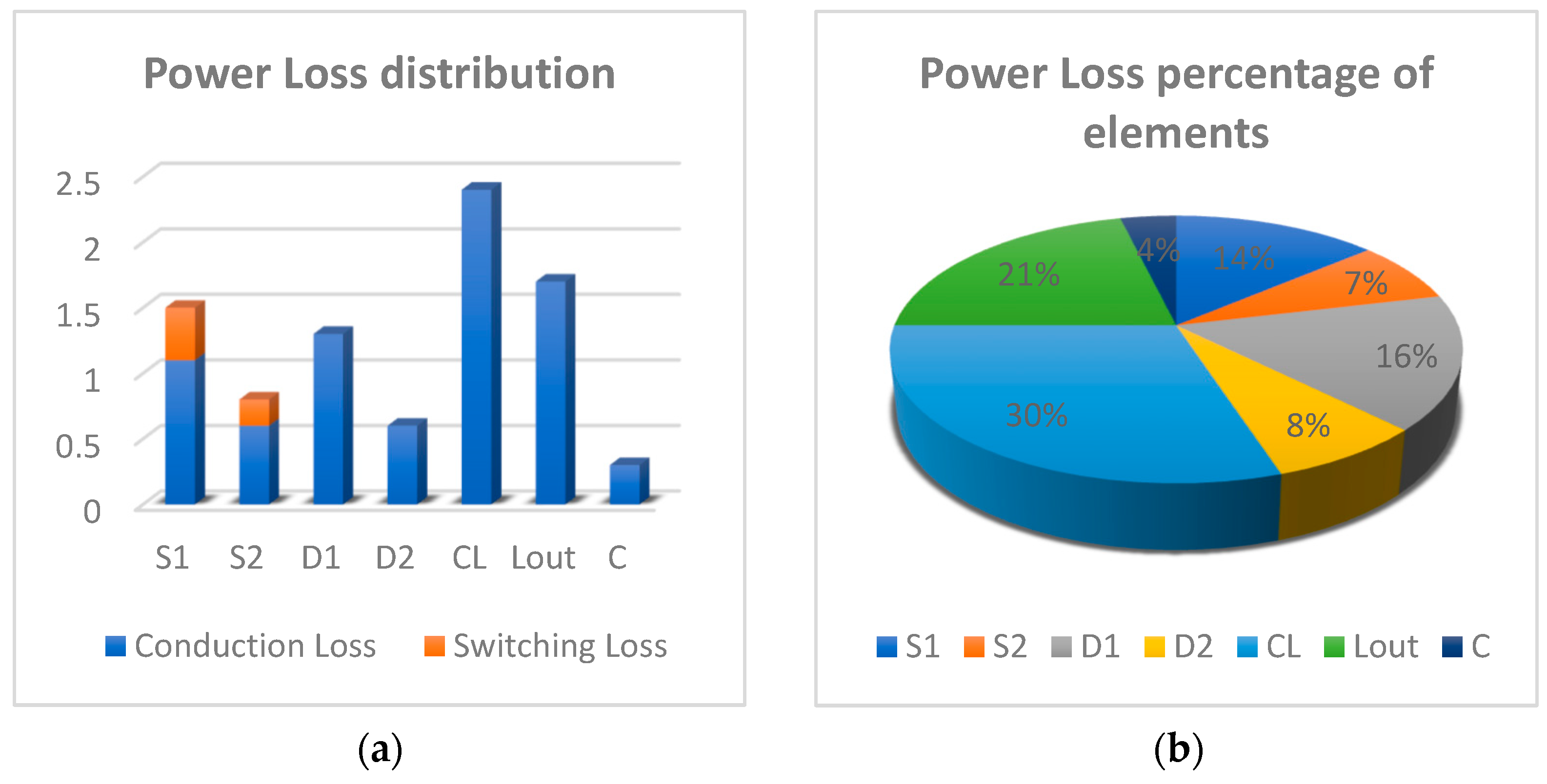
5. Stress and Power Loss Analysis

5.1. Voltage and Current Stress

Voltage stress ( V D S n ) across switches of the proposed converter is given below
V D S n = V i n
(24) Shows that the voltage stress across the switches is equal to the input voltage. Similarly, the current stress is the sum of output current ( I L o u t ) and the output inductor ripples.
I s t r e s s = I L o u t + Δ I L o u t

5.2. Power Loss Analysis

The major contributors to the power dissipation the proposed converter are the conduction losses of the parasitic components and switching losses of the MOSFET. The parasitic components, r D S n , r D n , V F n , r L n , and r c are the switch ON-state resistance, the diode’s forward resistance, the diode forward drop voltage, the inductor’s ESR, and the capacitor’s ESR respectively.
The conduction loss of the switches ( P c o n s n ) can be derived as
P c o n s n = I S n r m s 2 × r D S
The switching loss of the switches S 1 and S 2 ( P s w s n ) is given by
P s w n = f s × C e q × V D S n 2 2
where f s is switching frequency, C e q is the constant equivalent capacitance of the switch, and V D S n is the voltage stress across the switches. From Equation (24), V D S n = V i n , (27) can be written as
P s w n = f s × C e q × V i n 2 2
where I S n r m s is the switch rms current, and f s is the switching frequency. The conduction loss of the diodes ( P c o n D n ) is due to r D n and V F n . The estimated conduction loss is
P c o n D n = I D n a v g   ×   V F n + I D n r m s 2 × r D n
The conduction losses of the inductors are estimated as
P c o n L n = I L n r m s 2   ×   r L n
The conduction losses of the capacitor is given by
P c o n C n = I C n r m s 2   ×   r L n
The inductors also experience core losses in their operation. The core loss inductors are given by
P f e L o u t = l m × A c × K × f e × B m a x β P f e C L = l m × A c × K f e × B m a x β P f e t o t a l = P f e L o u t + P f e C L
where l m , A c , K f e , B m a x , and β represent the magnetic path length, the core’s cross-sectional area, the core loss coefficient, maximum flux density, and the core loss exponent, respectively.
In the experimental works, at an output power of 460 W, the component’s power loss breakdown is included to provide a clear analysis of the proposed converter, as shown in Figure 9a. Additionally, Figure 9b illustrates the percentage power loss distribution among the switch, diodes, inductors, and capacitors.

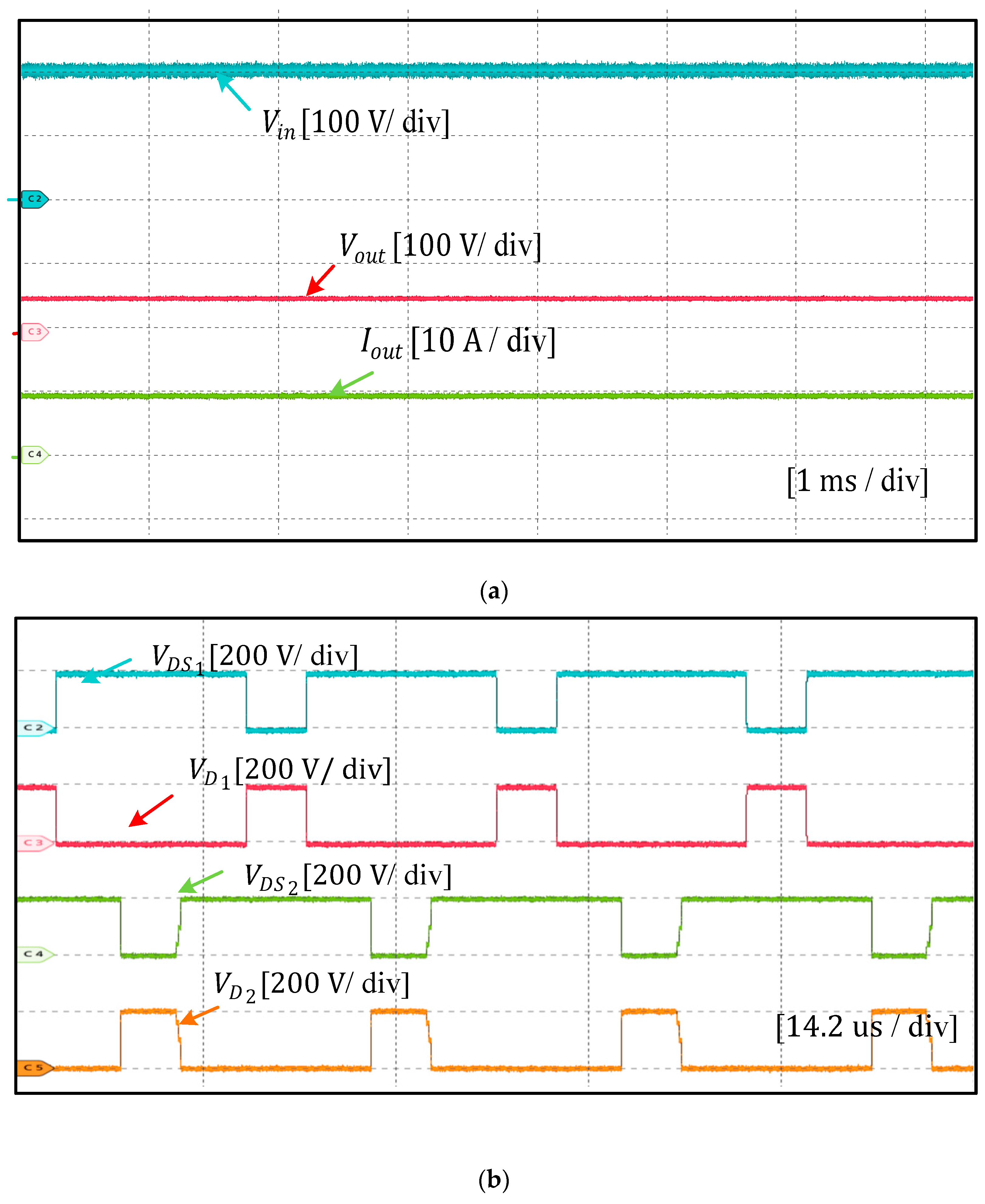
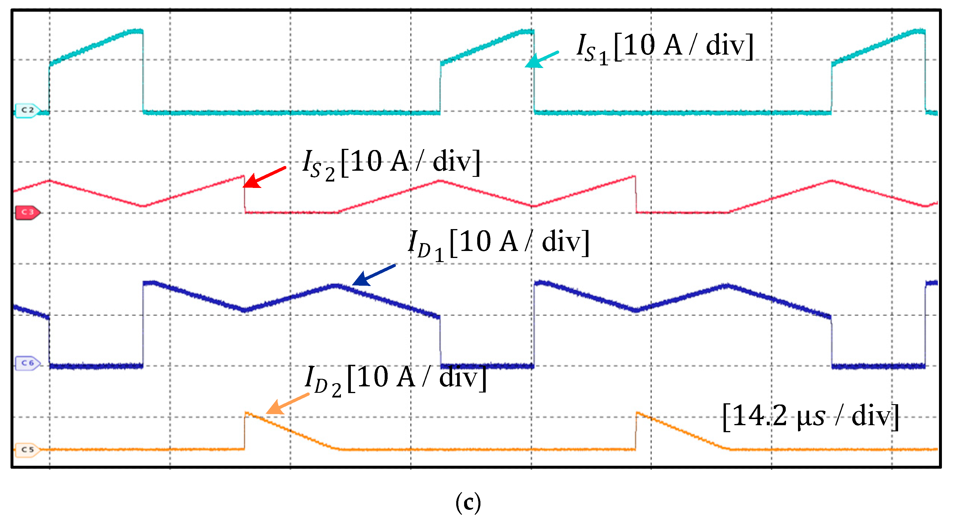
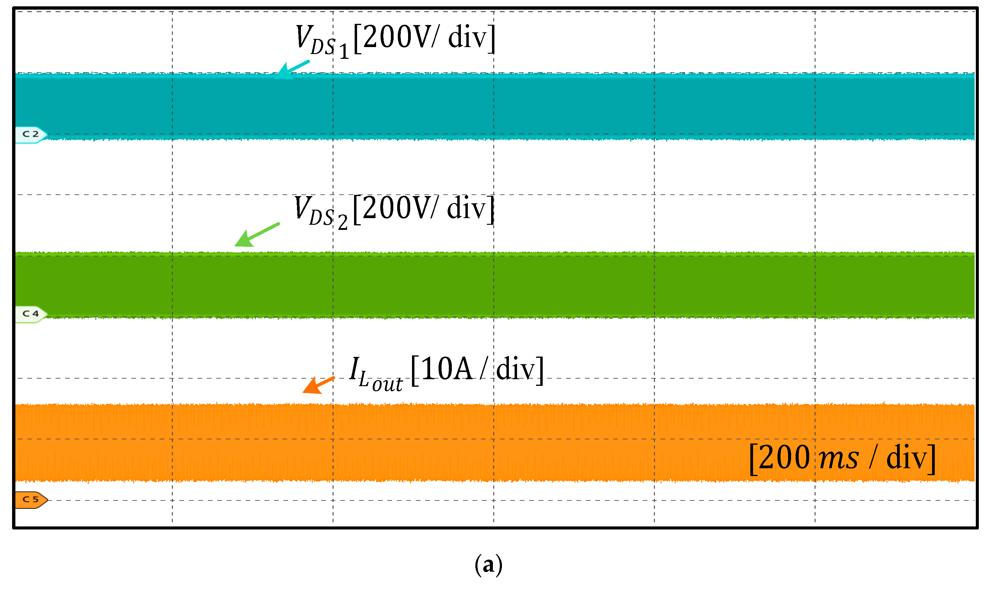
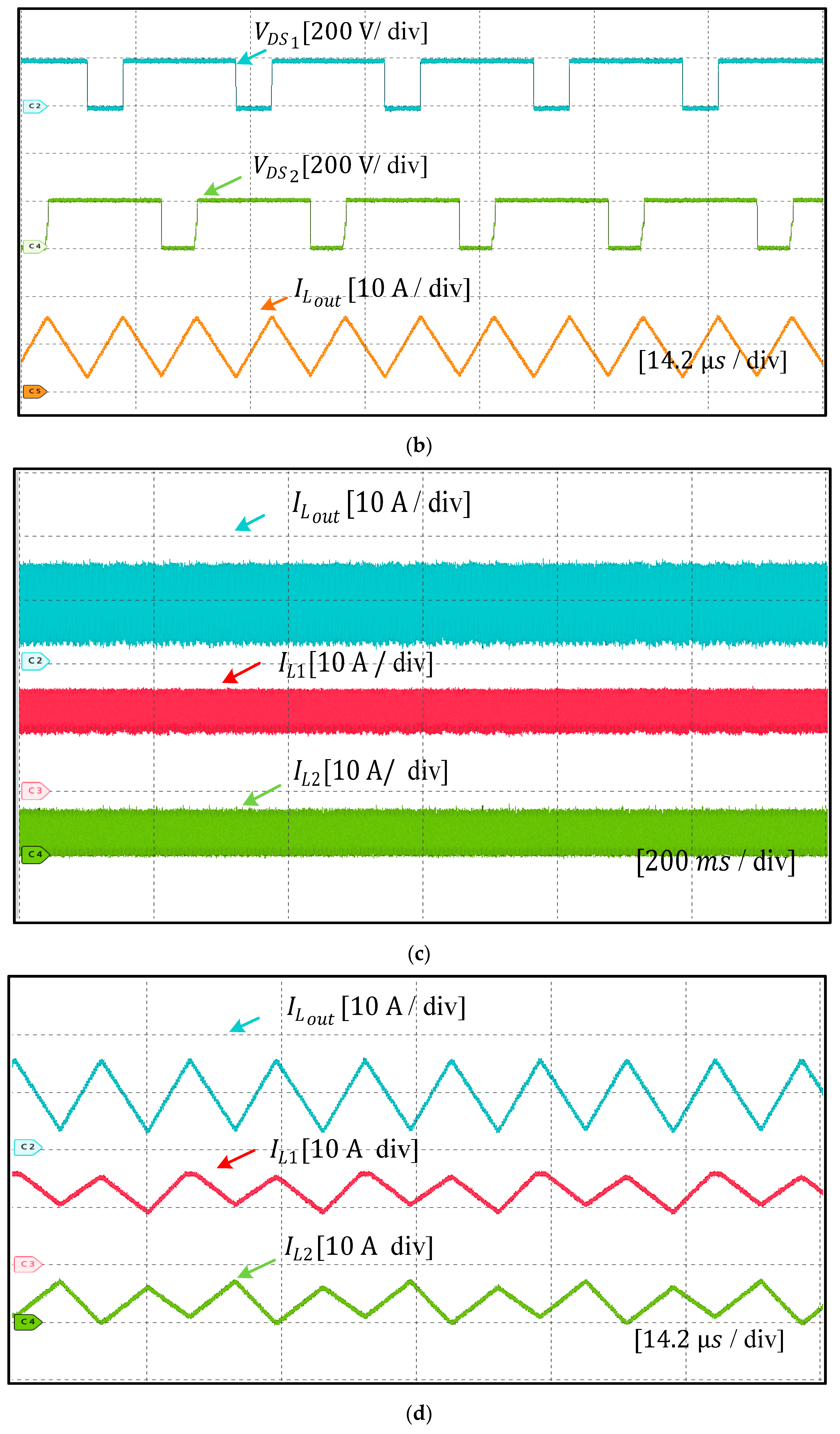
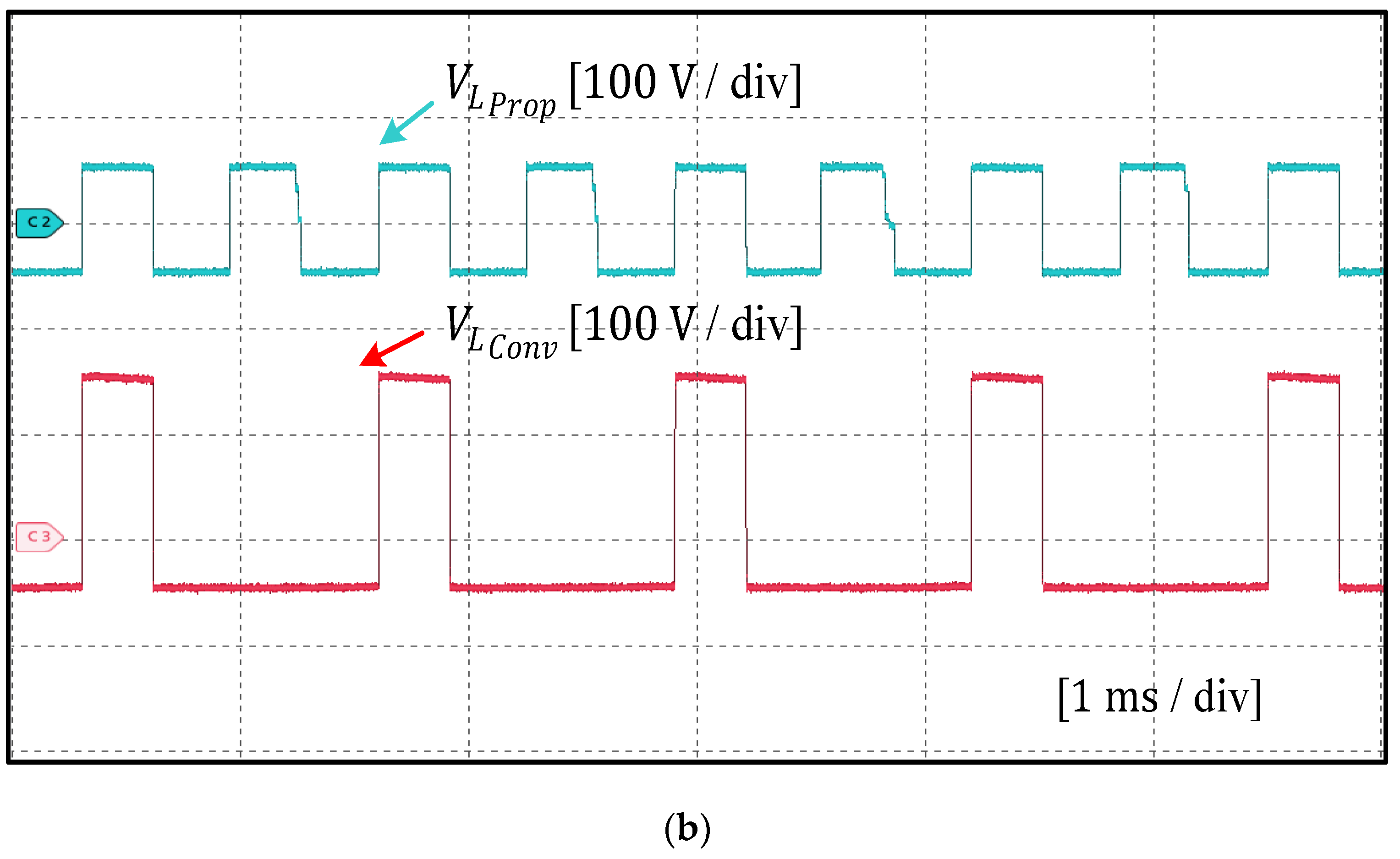
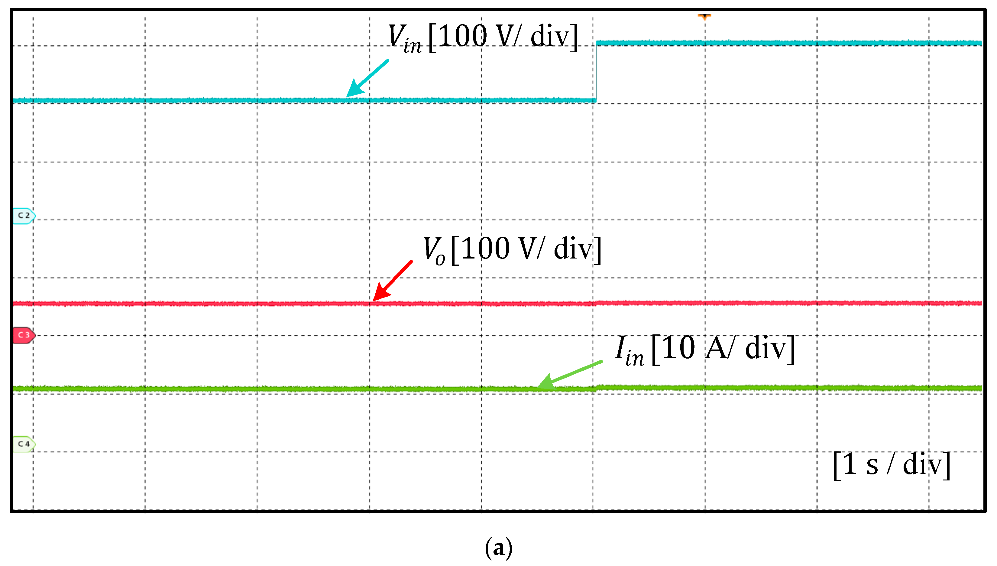
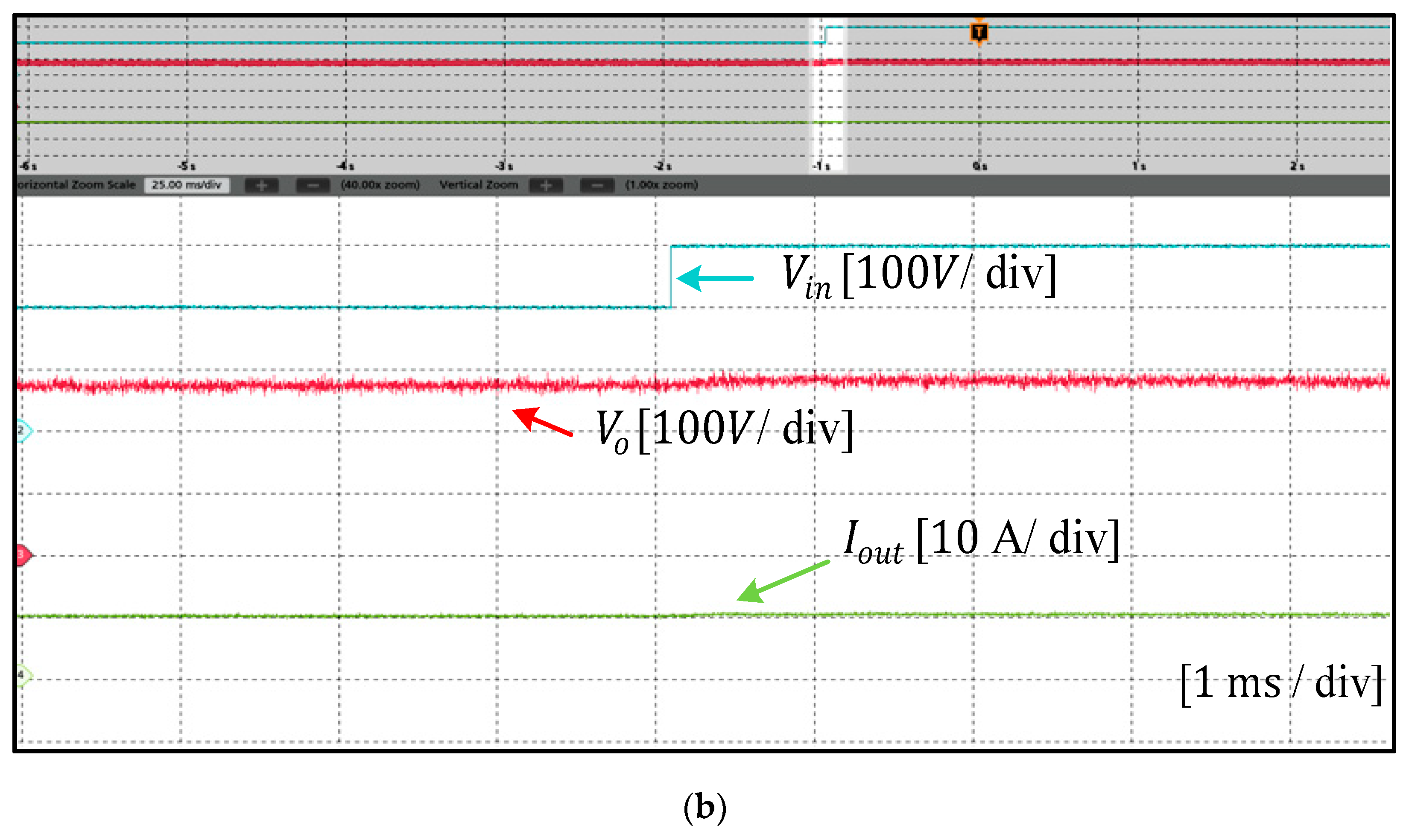
6. Experimental Results and Discussion

The experimental setup was designed based on the previous analysis. The proposed converter prototype was tested on a 460 W hardware prototype to verify its operations. Table 1 shows the electrical component specifications needed to build the prototype.
The experimental results were performed with a duty ratio less than 0.5. Figure 10 and Figure 11 illustrate the experimental results obtained with resistive load. Figure 10a show the input voltage ( V i n ), output voltage ( V o u t ) and output current ( I o u t )  Figure 10b shows the voltage stress across the switches ( V D S 1 , V D S 2 ) and diodes   ( V D 1 , V D 2 ). These results indicate that the voltage stress is equal to the input voltage of the proposed buck converter. Figure 10c shows current stress across the switches and diodes. Figure 11a provides the experimental results of the voltage stress across the switches ( V D S 1 , V D S 2 ) and the current through the output inductor ( I L o u t ). Figure 11b provide an expanded view of Figure 11a; it illustrates that the output inductor ( I L o u t ) frequency is twice the switching frequency, thus resulting in a lower ripple current. Similarly, Figure 11c simulation results of the output inductor current ( I L o u t ) along with coupled inductor currents ( I L 1 , I L 2 ). Figure 11d provide expanded view of Figure 11c. Furthermore, Figure 12a illustrates the inductor current of the proposed ( I L P r o p ) and conventional ( I L C o n v )   converter. From Figure 12b, the zoomed-in simulation results, it is evident that the current flowing through the inductor of the proposed converter for the same output voltage is very small compared to that of the conventional converter. Figure 13 shows the experimental result of the inductor’s voltages of the proposed and conventional converter   ( V L p r o p ,   V L C o n v ). These results clearly show that the voltage across the proposed converter’s inductor is minimal compared to the conventional converter. Figure 14 shows the response to the change in the input voltage; when the input voltage is increased from 200 V to 300 V, the corresponding output voltage and current remain stable. Figure 15 shows the experimental setup of the proposed converter.

7. Conclusions

This article introduces a non-isolated bidirectional DC-DC converter (BDC) designed for battery energy storage systems (BESSs). It thoroughly discusses the converter’s operating principles, specifications, and circuit parameter design. The proposed BDC is highlighted for its ability to handle low output currents, minimize component voltage stresses, and maintain a common ground across input and output ports, making it a suitable interface for battery storage applications. Additionally, using a small filter inductor reduces the output current ripple, effectively safeguarding the BESS and extending its operational lifespan. The experimental results illustrating the performance and ripple comparison further validate the effectiveness of this converter for BESS applications.

Author Contributions

Conceptualization, J.M.K. and A.A.K.; Investigation, A.A.K.; Methodology J.M.K.; Funding Acquisition, A.A.K.; Supervision, A.A.K.; Writing—Review and Editing J.M.K., A.A.K. and M.J. All authors have read and agreed to the published version of the manuscript.

Funding

This research was supported by Natural Sciences and Engineering Research Council of Canada (NSERC), Discovery Grant.

Data Availability Statement

The original contributions presented in the study are included in the article, further inquiries can be directed to the corresponding author/s.

Conflicts of Interest

The authors declare that there are no conflicts of interest regarding the publication of this paper.

References

  1. Edenhofer, O.; Pichs Madruga, R.; Sokona, Y.; IPCC (Eds.) Renewable Energy Sources and Climate Change Mitigation: Summary for Policymakers and Technical Summary; International Panel of Climate Change: Geneva, Switzerland, 2011; ISBN 978-92-9169-131-9. [Google Scholar]
  2. Wang, S.-P.; Liao, H.; Chen, J.-F. Design and Implementation of a Novel Bidirectional DC-DC Converter with Coupled Inductor. In Proceedings of the 2018 IEEE 7th World Conference on Photovoltaic Energy Conversion (WCPEC) (A Joint Conference of 45th IEEE PVSC, 28th PVSEC & 34th EU PVSEC), Waikoloa Village, HI, USA, 10–15 June 2018; IEEE: Piscataway, NJ, USA, 2018; pp. 644–649. [Google Scholar] [CrossRef]
  3. Esmaeili, S.; Shekari, M.; Rasouli, M.; Hasanpour, S.; Khan, A.A.; Hafezi, H. High Gain Magnetically Coupled Single Switch Quadratic Modified SEPIC DC-DC Converter. IEEE Trans. Ind. Appl. 2023, 59, 3593–3604. [Google Scholar] [CrossRef]
  4. Reddy, B.M.; Samuel, P. A comparative analysis of non-isolated bi-directional dc-dc converters. In Proceedings of the 2016 IEEE 1st International Conference on Power Electronics, Intelligent Control and Energy Systems (ICPEICES), Delhi, India, 4–6 July 2016; IEEE: Piscataway, NJ, USA, 2016; pp. 1–6. [Google Scholar] [CrossRef]
  5. Mumtaz, F.; Zaihar Yahaya, N.; Tanzim Meraj, S.; Singh, B.; Kannan, R.; Ibrahim, O. Review on non-isolated DC-DC converters and their control techniques for renewable energy applications. Ain Shams Eng. J. 2021, 12, 3747–3763. [Google Scholar] [CrossRef]
  6. Parimalasundar, E.; Maneesha, S.; Hanish, R.; Reddy, P.M.; Harish, P.K.; Rao, P.K. Performance Analysis of DC-DC Converter for Electric Vehicle Charging Applications. In Proceedings of the 2023 7th International Conference on Computing Methodologies and Communication (ICCMC), Erode, India, 23–25 February 2023; IEEE: Piscataway, NJ, USA, 2023; pp. 1543–1546. [Google Scholar] [CrossRef]
  7. Wang, Z.; Wang, P.; Li, B.; Ma, X.; Wang, P. A Bidirectional DC–DC Converter with High Voltage Conversion Ratio and Zero Ripple Current for Battery Energy Storage System. IEEE Trans. Power Electron. 2021, 36, 8012–8027. [Google Scholar] [CrossRef]
  8. Chub, A.; Vinnikov, D.; Kosenko, R.; Liivik, E.; Galkin, I. Bidirectional DC–DC Converter for Modular Residential Battery Energy Storage Systems. IEEE Trans. Ind. Electron. 2020, 67, 1944–1955. [Google Scholar] [CrossRef]
  9. Santra, S.B.; Chatterjee, D.; Siwakoti, Y.P. Coupled Inductor Based Soft Switched High Gain Bidirectional DC-DC Converter with Reduced Input Current Ripple. IEEE Trans. Ind. Electron. 2023, 70, 1431–1443. [Google Scholar] [CrossRef]
  10. Filsoof, K.; Lehn, P.W. A Bidirectional Modular Multilevel DC–DC Converter of Triangular Structure. IEEE Trans. Power Electron. 2015, 30, 54–64. [Google Scholar] [CrossRef]
  11. Ahmad, A.; Singh, R.K.; Mahanty, R. Bidirectional quadratic converter for wide voltage conversion ratio. In Proceedings of the 2016 IEEE International Conference on Power Electronics, Drives and Energy Systems (PEDES), Trivandrum, India, 14–17 December 2016; IEEE: Piscataway, NJ, USA, 2016; pp. 1–5. [Google Scholar] [CrossRef]
  12. Khan, A.A.; Cha, H.; Lai, J.-S. Cascaded Dual-Buck Inverter with Reduced Number of Inductors. IEEE Trans. Power Electron. 2018, 33, 2847–2856. [Google Scholar] [CrossRef]
  13. Forouzesh, M.; Siwakoti, Y.P.; Gorji, S.A.; Blaabjerg, F.; Lehman, B. Step-Up DC–DC Converters: A Comprehensive Review of Voltage-Boosting Techniques, Topologies, and Applications. IEEE Trans. Power Electron. 2017, 32, 9143–9178. [Google Scholar] [CrossRef]
  14. Fardahar, S.M.; Sabahi, M. New Expandable Switched-Capacitor/Switched-Inductor High-Voltage Conversion Ratio Bidirectional DC–DC Converter. IEEE Trans. Power Electron. 2020, 35, 2480–2487. [Google Scholar] [CrossRef]
  15. Hulea, D.; Muntean, N.; Gireada, M.; Cornea, O.; Serban, E. Bidirectional Hybrid Switched-Inductor Switched-Capacitor Converter Topology with High Voltage Gain. In Proceedings of the 2019 21st European Conference on Power Electronics and Applications (EPE ’19 ECCE Europe), Genova, Italy, 3–5 September 2019; IEEE: Piscataway, NJ, USA, 2019; pp. P.1–P.10. [Google Scholar] [CrossRef]
  16. Khan, A.A.; Eberle, W.; Wang, L.; Akbar, F.; Khan, U.A.; Lu, Y.W.; Agamy, M. Coupled-Inductor Buck–Boost Inverter with Reduced Current Ripple. IEEE Trans. Power Electron. 2020, 35, 7933–7946. [Google Scholar] [CrossRef]
  17. Ismail, A.H.; Ma, Z.; Al-Hmoud, A.; Zhao, Y. A High Frequency Coupled Inductor Design for High Power Density DC-DC Converters. In Proceedings of the 2023 IEEE Applied Power Electronics Conference and Exposition (APEC), Orlando, FL, USA, 19–23 March 2023; IEEE: Piscataway, NJ, USA, 2023; pp. 3275–3280. [Google Scholar] [CrossRef]
  18. Zhu, G.-R.; Tan, S.-C.; Chen, Y.; Tse, C.K. Mitigation of Low-Frequency Current Ripple in Fuel-Cell Inverter Systems through Waveform Control. IEEE Trans. Power Electron. 2013, 28, 779–792. [Google Scholar] [CrossRef]
  19. Abeywardana, D.B.W.; Hredzak, B.; Fletcher, J.E.; Konstantinou, G. A cascaded boost inverter based battery energy storage system with reduced battery ripple current. In Proceedings of the IECON 2017-43rd Annual Conference of the IEEE Industrial Electronics Society, Beijing, China, 29 October–1 November 2017; IEEE: Piscataway, NJ, USA, 2017; pp. 2733–2738. [Google Scholar]
  20. Lee, P.-W.; Lee, Y.-S.; Cheng, D.K.W.; Liu, X.-C. Steady-state analysis of an interleaved boost converter with coupled inductors. IEEE Trans. Ind. Electron. 2000, 47, 787–795. [Google Scholar] [CrossRef]
  21. Leal, W.C.; Godinho, M.O.; Bastos, R.F.; De Aguiar, C.R.; Fuzato, G.H.F.; Machado, R.Q. Cascaded Interleaved DC–DC Converter for a Bidirectional Electric Vehicle Charging Station. IEEE Trans. Ind. Electron. 2024, 71, 3708–3717. [Google Scholar] [CrossRef]
  22. Scire, D.; Lullo, G.; Vitale, G. Design and Modeling of an Interleaving Boost Converter with Quasi-Saturated Inductors for Electric Vehicles. In Proceedings of the 2020 AEIT International Conference of Electrical and Electronic Technologies for Automotive (AEIT AUTOMOTIVE), Turin, Italy, 18–20 November 2020; IEEE: Piscataway, NJ, USA, 2020; pp. 1–6. [Google Scholar] [CrossRef]
  23. Sferlazza, A.; Garraffa, G.; Vitale, G.; D’Ippolito, F.; Alonge, F.; Lullo, G.; Busacca, A.; Giaconia, G.C.; Scirè, D. Robust Disturbance Rejection Control of DC/DC Interleaved Boost Converters with Additional Sliding Mode Component. In Proceedings of the 2023 Asia Meeting on Environment and Electrical Engineering (EEE-AM), Hanoi, Vietnam, 13–15 November 2023; IEEE: Piscataway, NJ, USA, 2023; pp. 1–6. [Google Scholar] [CrossRef]
  24. Akbar, F.; Cha, H.; Ahmed, H.F.; Khan, A.A. A Family of Single-Stage High-Gain Dual-Buck Split-Source Inverters. IEEE J. Emerg. Sel. Top. Power Electron. 2020, 8, 1701–1713. [Google Scholar] [CrossRef]
  25. Khan, A.A.; Cha, H.; Ahmed, H.F. An Improved Single-Phase Direct PWM Inverting Buck–Boost AC–AC Converter. IEEE Trans. Ind. Electron. 2016, 63, 5384–5393. [Google Scholar] [CrossRef]
  26. Khan, A.A.; Cha, H.; Ahmed, H.F. High-Efficiency Single-Phase AC–AC Converters without Commutation Problem. IEEE Trans. Power Electron. 2016, 31, 5655–5665. [Google Scholar] [CrossRef]
Figure 1. Proposed DC-DC buck converter.
Energies 17 03570 g001
Figure 2. Proposed PWM scheme. (a) Switching signal generation; (b) switching waveform.
Energies 17 03570 g002
Figure 3. Proposed converter operation modes. (a) Mode 1 for D < 0.5 and D > 0.5. (b) Mode 2, Mode 4 for D < 0.5. (c) Mode 2, Mode 4 for D > 0.5. (d) Mode 3 for D < 0.5 and for D > 0.5.
Energies 17 03570 g003
Figure 4. Couple inductor and common mode current.
Energies 17 03570 g004
Figure 5. Key simulation waveforms: (a) D < 0.5; (b) D > 0.5.
Energies 17 03570 g005
Figure 6. Non-ideal model of the proposed converter.
Energies 17 03570 g006
Figure 7. Output current ripple comparison of the proposed and conventional buck converter.
Energies 17 03570 g007
Figure 8. Output inductance comparison of the conventional versus the proposed converter.
Energies 17 03570 g008
Figure 9. Power loss analysis. (a) Conduction and switching loss of elements. (b) Component-wise percentage loss.
Energies 17 03570 g009
Figure 10. Experimental results: (a) Input voltage ( V i n ), output voltage ( V o u t ), output current ( I o u t ) (b) Drain source voltages of switches ( V D S 1 , V D S 2 ) and voltage stress across diodes ( D 1 , D 2 ). (c) Current stress across switches and diodes.
Energies 17 03570 g010aEnergies 17 03570 g010b
Figure 11. Experimental results. (a) Expanded results of the voltages stress ( V D S 1 , V D S 2 ) and ( I L o u t ). (b) Zoomed-in simulation results of (a). (c) Expanded simulation results of I L o u t and ( I L 1 , I L 2 ). (d) Zoomed-in simulation results of (c).
Energies 17 03570 g011aEnergies 17 03570 g011b
Figure 12. Experiment results. (a) Inductor current of the proposed ( I L P r o p ) and conventional ( I L C o n v )   converter. (b) Zoomed-in results of (a).
Energies 17 03570 g012
Figure 13. Experimental results. (a) Expanded results of inductor voltage of the proposed and conventional converter   ( V L C o n v ,   V L C o n v ). (b) Zoomed-in results of (a).
Energies 17 03570 g013aEnergies 17 03570 g013b
Figure 14. Experimental results. (a) Expanded results of variations in input voltage vs. output voltage and current. (b) Zoomed-in results of (a).
Energies 17 03570 g014aEnergies 17 03570 g014b
Figure 15. Experimental setup.
Energies 17 03570 g015
Table 1. Component specifications.
ComponentsValues
Input   voltage   ( V i n )200 V
Output   voltage   ( V o u t ) 48 V
Rated output power460 W
MOSFET   ( S 1 ,   S 2 )NTHL065N65S3HF (ONSEMI, St.John’s, NL, Canada)
Switching frequency50 Khz
Diodes   ( D 1 , D 2 )BYC30JT-600PSQ
ControllerTMS320F28335
Inductors   ( L o u t )0.1 mH
Output   Capacitor   ( C O )100 μ F
Disclaimer/Publisher’s Note: The statements, opinions and data contained in all publications are solely those of the individual author(s) and contributor(s) and not of MDPI and/or the editor(s). MDPI and/or the editor(s) disclaim responsibility for any injury to people or property resulting from any ideas, methods, instructions or products referred to in the content.

