Article

Research on the Control and Modulation Scheme for a Novel Five-Switch Current Source Inverter

1
College of Electronic Engineering, Zhengzhou Railway Vocational & Technical College, Zhengzhou 451460, China
2
Inverter Technologies Engineering Research Center of Beijing, North China University of Technology, Beijing 100144, China
3
College of Electrical and Information Engineering, Hunan University, Changsha 410082, China
*
Authors to whom correspondence should be addressed.
Energies 2024, 17(15), 3640; https://doi.org/10.3390/en17153640
Submission received: 30 May 2024 / Revised: 11 July 2024 / Accepted: 15 July 2024 / Published: 24 July 2024

Abstract

:
Different from the voltage source inverter (VSI), the current source inverter (CSI) can boost the voltage and eliminate the additional passive filter and dead time. However, the DC-side inductor current is not a real current source and is generated by a DC voltage supply and an inductor. Under different switching states, the DC-side inductor will be charged or discharged, which leads to the DC-side inductor current being discontinuous or increasing. To solve the control problem of the DC-side inductor current of the CSI, a novel single-phase CSI topology with five switching tubes for grid-connected applications is proposed. Firstly, the reference calculation method and the hysteresis loop control scheme for the DC-side inductor current are proposed, and the adjustable and constant DC-side inductor current are obtained. Since the PWM signals cannot be directly implemented to the switching tubes, the modulation strategy for the single-phase CSI is proposed in this paper. Then, an active damping method based on the feedback capacitor voltage is presented to suppress the resonance peak caused by the LC filter on the grid side. Finally, the math model of the AC-side structure is established, and the optimal proportional-resonant controller parameters’ design method is explored by the amplitude–frequency characteristic curves. The simulation and experiment are implemented for the proposed CSI topology. The results show that a high-quality power with a good control performance can be obtained with the proposed CSI topology.

1. Introduction

To reduce carbon emissions and environmental pollution, it is imperative to accelerate the extraction of non-fossil fuels, such as wind power and photovoltaic power generation [1,2]. The inverter is the core part of a grid-connected device, used to complete the conversion of electrical energy from DC to AC, and it includes a voltage source inverter (VSI) and current source inverter (CSI) [3]. The VSIs stand out for their simple topology and flexible modulation and are employed in motor drives, electric vehicles, new energy generation, and other power conversion scenarios [4]. However, when the VSI is connected to the power grid, since the inverter output voltage contains switching harmonics, it is necessary to add a large inductor or LCL-type filter between the inverter and the grid side [5]. Although an L-type filter has a simple structure and no resonance, it has a large volume, poor dynamic characteristics, and insufficient suppression of the harmonics at the switching frequency [6]. The LCL-type filter is a third-order system, and a resonance peak occurs in the Bode plots of the LCL filter, which increases the complexity of the control system [7].
Different from VSIs, a CSI has the unique advantages of boost characteristic, protection for short circuits and overcurrent, no need for an electrolytic capacitor, and low dv/dt stress [8,9]. In the AC side, the capacitor filter and the grid-side inductor together form an LC-type second-order filter, which has a high filtering performance for high-frequency harmonics [10], and its resonance peak is lower than that of the LCL-type filter. However, the traditional CSI, shown in Figure 1, has some inherent shortcomings, which limits its wide application. Firstly, the DC-side inductor current of the CSI is not provided by a real current source, but is generated by a DC voltage source charging to the DC-side inductor. Different switching states have an impact on the charging or discharging of the DC-side inductor, and, as the DC-side inductor current and the AC-side output voltage have a coupling relationship, the control of the DC-side inductor current is necessary to improve the practicability of the CSI [11].
For example, if the initial value of the DC-side inductor current idc is zero, idc is in a discontinuous state, the amplitude of the load current is is relatively low, and there is an obvious low-order harmonic, which is shown in Figure 2a. This is because idc is too low to provide enough current for the AC-side load; the duration of the pass-through state is too short, causing the DC-side inductor to be unable to be sufficiently charged; the amplitude of is is lower than that of idc; and is cannot maintain a sinusoidal shape. When the initial value of idc is much greater than the amplitude of is, the simulation waveforms are as shown in Figure 2b. Within a fundamental cycle, since the charging effect of the DC-side inductor is greater than the discharging effect, idc continues to increase, which leads to the duration of the non-pass-through state decreasing and the duration of the pass-through state increasing. idc and the duty cycle of the pass-through state are a positive feedback process. Meanwhile, the higher harmonics of is increase with the decrease in the current utilization rate.
Secondly, the traditional CSI cannot operate in buck mode, and the waveforms are similar to those Figure 2b. Because the DC-side inductor is continuously charged, it is an unacceptable state for the CSI [12]. In summary, there is a coupling effect between the AC and DC sides of the traditional CSI, and it is difficult to control idc. In response to these challenges, a DC-side inductor current inner-loop controller was added into the AC control loop [11]. Due to too many state variables in the control system, this approach cannot achieve decoupling of the DC-side inductor current and the AC-side voltage. The second harmonic occurs in the DC-side inductor current, and the grid current has obvious low-order harmonic distortion. Therefore, the topology improvement of the CSI is the most widely used approach to achieve the DC-side inductor current control and voltage buck operation. A variety of two-stage improved topologies for the CSI have been proposed. The CSI with the quasi-Z source network proposed in [13] can achieve the buck operation without adding power-switching devices; this topology is shown in Figure 3a, where the red dots represent the same name terminal of the transformer. However, the introduction of too many passive devices greatly increases the complexity of the system and is not conducive to the design of the control system. Another topology, presented in [14], includes a front-stage rectifier and a back-stage inverter. This topology enables the control of the DC-side inductor current by the rectifier bridge, but it is only suitable for the wind power generation and other AC–DC–AC power conversion scenarios. Reference [15] added an SEPIC circuit on the DC side of the CSI to achieve the buck operation and common-mode current suppression. However, the SEPIC circuit includes three switching tubes, one diode, and two capacitors, which increases the loss and cost of the CSI. In [16], a switching tube and a diode were in parallel with the DC-side inductor, as shown in Figure 3b, and a new switching state was added to provide another freewheeling loop for the DC-side inductor. By switching to the pass-through state, the control and stability of idc can be achieved. In [17], a buck–boost CSI topology, shown in Figure 3c, was proposed to achieve the buck operation. However, the coupling between the DC side and the AC side was not eliminated by the topologies proposed in [16,17]. A CSI topology with a two-transistor forward voltage–current (V–I) converter was proposed in [18] and is shown in Figure 3d; the control for the DC-side inductor current and the buck operation can be realized. This topology also decouples the V–I converter from the CSI inverter, enabling independent control and bidirectional energy flow.
In addition to the different characteristics of the DC-side energy source, the switching signal generation method of the CSI is very different to that of VSI. Since the CSI allows bridge arm short circuits but not open circuits, the PWM signals, generated by comparison between the modulation signal and the carrier signal, cannot be directly implemented to the switching tubes of the CSI [19]. For this reason, Reference [20] proposed a logic circuit that converts two-value logic signals to three-logic logic signals, but it will increase the delay of the driving signal. In addition, the grid-side LC filter has a resonance peak phenomenon, which needs to be suppressed through the active damping method [21]. An active damping method was adopted in [22], which adopts the feedback of the AC-side capacitive current to reduce the resonance peak, but it requires additional current sensors, and the digital delay is not considered.
To fully utilize the advantages of the CSI and overcome its inherent defects, in this paper, a novel single-phase grid-connected CSI with five switching tubes is taken as the research object, and the operation principle is presented in Section 2. The reference calculation and hysteresis control scheme of the DC-side inductor current are proposed in Section 3. Aiming at the problem that the PWM signals cannot be directly implemented to the switching tubes of the CSI, the logical converter expressions are derived in Section 4. In Section 5, on the premise of introducing the capacitor voltage feedback channel, the amplitude–frequency characteristics of the closed-loop transfer function and the disturbance transfer function under different proportional resonant controller parameters are analyzed, and the method for determining the controller parameters is obtained. Finally, the simulation and experimental verifications are completed in Section 6 and Section 7, respectively. The conclusion is given in Section 8.

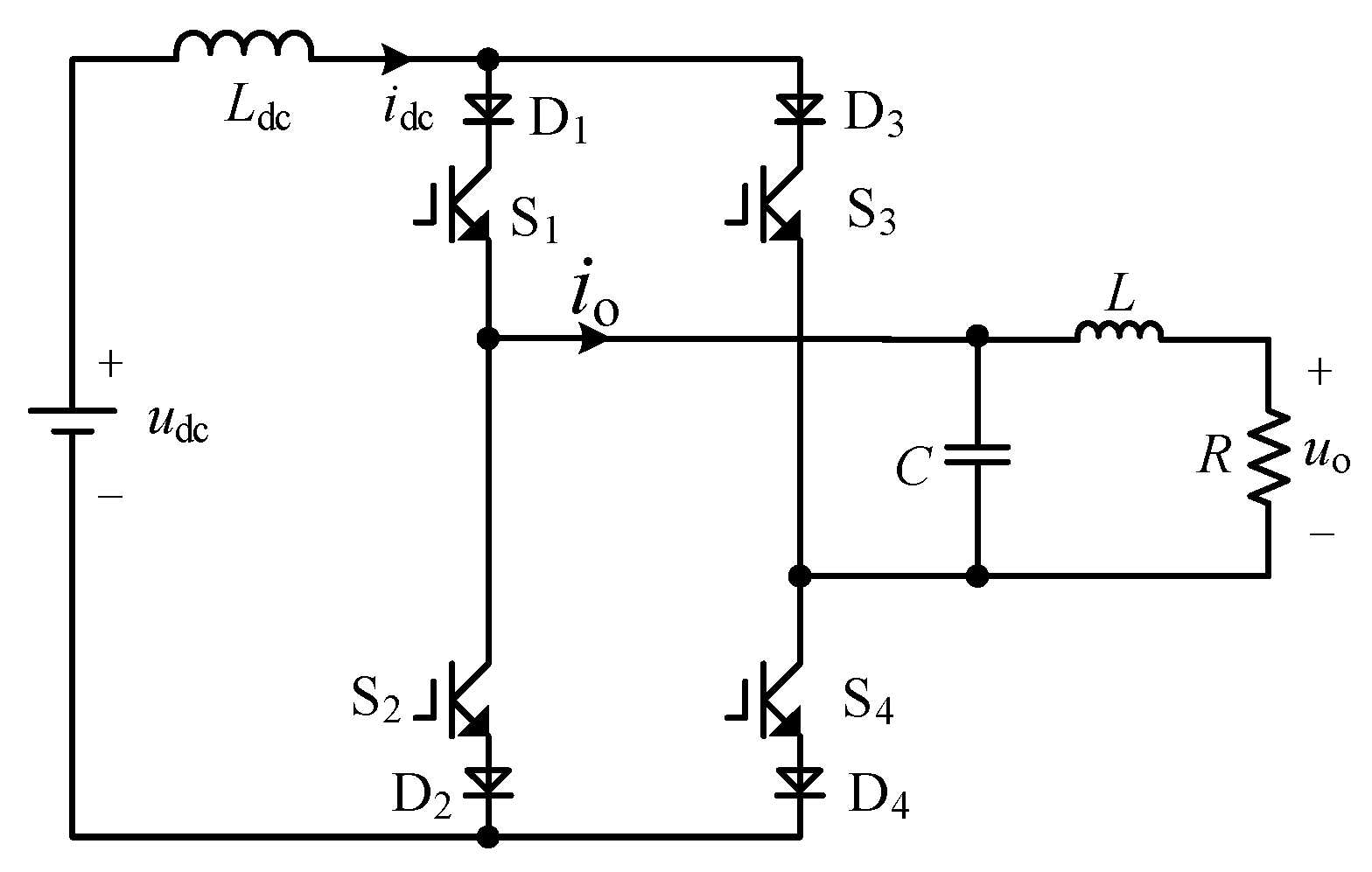
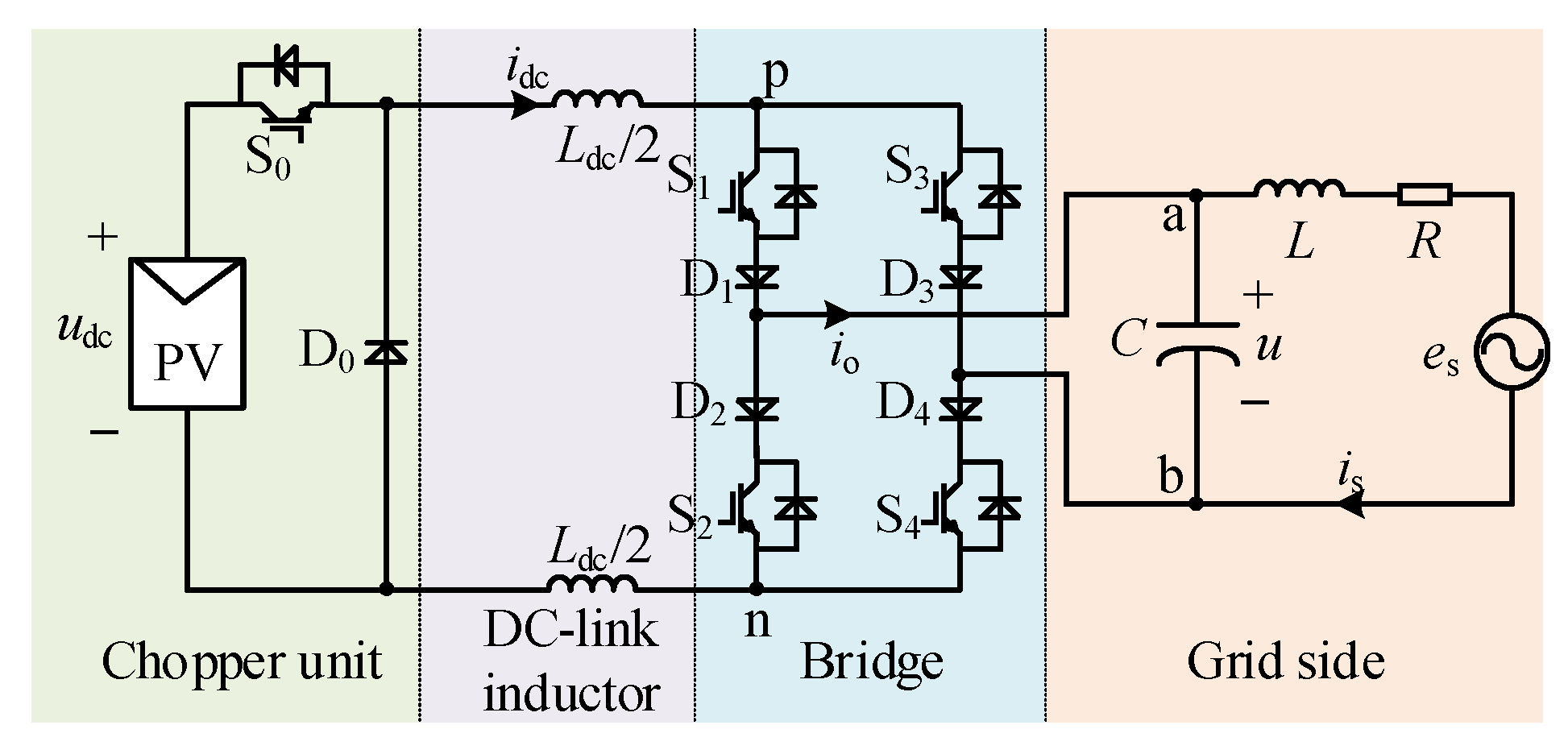
2. Topology and Operation Principle of the Proposed CSI Topology

After analyzing and comparing various improved CSI topologies, the CSI with the V–I converter proposed in [18] is the optimal topology. The DC-side inductor current can be controlled as a controlled current source, the coupling effect with the AC-side can be eliminated, and the improved CSI can operate in the buck, boost, and regeneration modes. Since the application scenario of this paper is the grid-connected system, the direction of the energy is only from the DC side to the AC side, so the V–I converter is replaced by a simple buck unit in this paper, and only one switching tube and one diode are introduced. A stable DC-side inductor current can be obtained, and the CSI can operate in the buck mode.
The proposed five-switch single-phase grid-connected CSI with a DC-buck unit is shown in Figure 4. udc denotes the DC-side input voltage; the switching tube S0 and diode D0 constitute the DC chopper unit, which realizes the adjustment of the DC-side inductor current idc. Switching tubes S1–S4 and diodes D1–D4 constitute the CSI bridge; L, R, C, and es denote the grid-side inductance, resistance, filtering capacitance, and voltage, respectively, which denotes the gird.
According to Figure 4, the state equation of the DC-side inductor current idc is derived as follows:
L dc d i dc d t = u dc p 0 u pn
where p0 denotes the switching function of the switching S0, upn denotes the voltage between the upper and lower DC bus of the bridge, and upn satisfies the following relationship:
u pn = u ab p inv
where uab is the voltage of the filter capacitor and pinv denotes the switching function, and pinv is defined as follows:
p inv = 1             S 1       S 4       on ,       S 2       S 3       off 0             S 1       S 2       on ,       S 3       S 4       off       1         S 2       S 3       on ,       S 1       S 4       off
The state equation of uab can be derived and is shown as follows:
d u ab d t = i o i s
where io is the output current of bridge, and is the grid-side current, respectively. io should be equal to idc × pinv, and the state equation of is derived as follows:
L s d i s d t = u ab i s R s e s
According to Equations (1) and (5), the switching action induces changes in idc, which in turn affects uab. There is a significant coupling relationship between uab and idc. To remove coupling between AC and DC sides, the DC-side inductor current and the grid current are decomposed into two separate links. The constant output of idc is achieved by adjusting the switching state of S0, and the control of grid current is achieved by controlling S1–S4.

3. Reference Calculation and Control Scheme for DC-Side Inductor Current

The loss of the switching tubes, and the harmonic distortion of the current exhibit a positive correlation with the DC-side inductor current. Therefore, under the condition that the DC-side inductor current is capable of meeting power requirements, the current utilization rate should also be improved as much as possible.

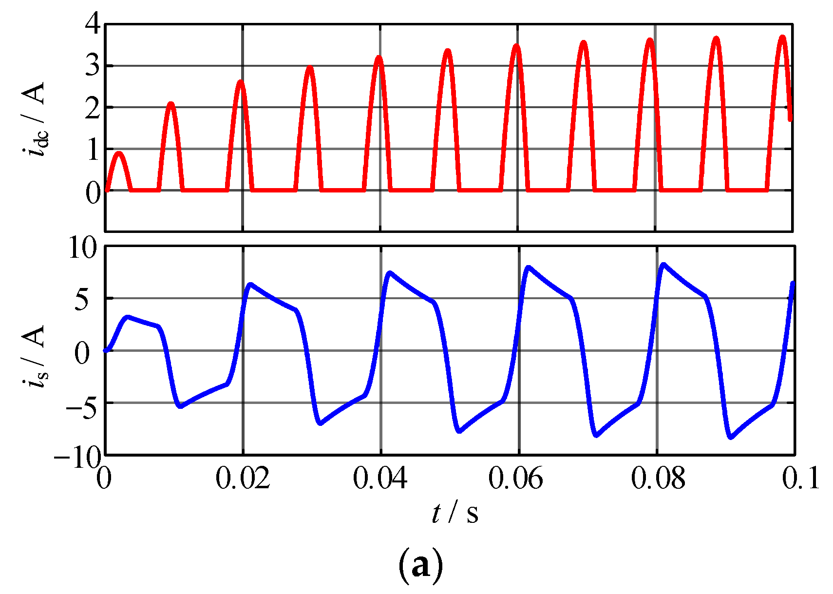
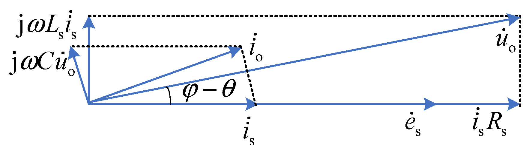
3.1. Reference Calculation for DC-Side Inductor Current

The vector diagram of the inductor, capacitor, resistor, and grid voltage in the AC side is shown in Figure 5.
The expression for the grid voltage, es, is defined as follows:
e s ( t ) = E s sin ( ω t + θ )
where Es denotes the magnitude of es, θ denotes the initial phase, and ω denotes the angular frequency. When the CSI operates at steady state and at unit power factor, is, the expression of the grid current, is defined as follows:
i s ( t ) = I s sin ( ω t + θ )
where Is denotes the fundamental amplitude of is. According to the circuit, the fundamental wave expression of uab is defined as follows:
u ab ( t ) = U sin ( ω t + φ )
where U and φ denote the amplitude and phase of uab. They can be derived as follows:
U = ( ω L s I s ) 2 + ( E s + I s R ) 2 φ = θ + arctan ( ω L s I s E s + I s R )
According to the vector diagram of the AC grid side, based on the cosine theorem, the expression for the fundamental amplitude Io of io can be derived as follows:
I o = ω 2 C 2 U o 2 + I s 2 2 ω C U o I s sin ( φ θ )
Substituting (9) into (10), Io is obtained as follows:
I o = ω 2 C 2 ( E s + I s R ) 2 + ω 4 C 2 L s 2 I s 4 + ( 1 ω 2 L s C ) 2 I s 2
where io is modulated by idc. The reference of idc is equal to Io/m, where m is the modulation ratio. If m is set too high, Ldc cannot be charged sufficiently in the through state; it is difficult to achieve a volt-second balance of the DC-link inductor. If m is set too low, the current utilization rate is too low, and the loss is also great. Therefore, under the condition that the DC-side inductor current is capable of meeting power requirements, the current utilization rate should also be improved as much as possible. According to [18], m is set as 0.75 in this paper.

3.2. Hysteresis Loop Control Scheme for DC-Side Inductor Current

To realize the DC-side inductor current following the reference value i dc * , as shown in Figure 6, an easy-to-implement hysteresis control scheme is adopted in this paper. When idc is greater than the hysteresis loop upper limit setting value, S0 is turned off, Ldc provides energy to the load alone during this period, and idc gradually decreases. When idc is lower than the hysteresis lower limit setting value, S0 is turned on, udc charges Ldc in the stage of pass-through state and non-pass-through state when udc is greater than uo, and idc continuously increases.

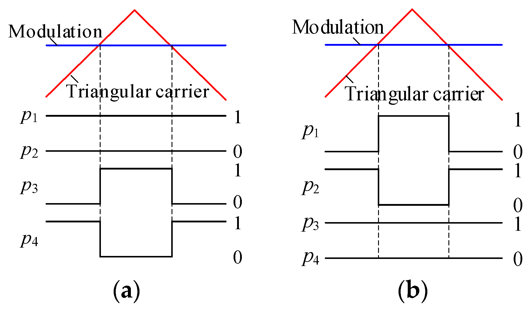
4. Modulation Strategy for the CSI

Different from the VSI, the PWM signals generated by the comparison between the modulation signal and the carrier signal cannot be directly implemented for the switching tubes of CSI. Instead, a logic conversion process is necessary. Since the single-phase modulation strategy is relatively simple, there is no need to adopt hardware logic circuit, and the switching signals of S1–S4 can be directly generated by the digital signal processor. A logic signal X is defined, and, determined by the polarity of the judgment method, is defined as follows:
X = 1 i o * 0 0 i o * < 0  
Another logic signal Y is defined; it is used to reflect the pass-through state and the non-pass-through state of CSI, and is determined by the compared result between the modulating signal and the triangular carrier signal; the judgment method is defined as follows:
Y = 1 i o * / i dc   triangular   carrier 0 i o * / i dc <   triangular   carrier  
Combining the inverter bridge switching functions shown in Equation (3), the drive logic functions p1p4 for S1–S4 are obtained.
p 1 = X | Y ¯ p 2 = X ¯ & Y p 3 = X ¯ | Y ¯ p 4 = X & Y
When i o * > 0, X = 1; at this time, S1 is turned on, and S2 is turned off. Commutation occurs between S3 and S4, CSI switches between pass-through and non-pass-through states, and the diagram of p1p4 is shown in Figure 7a. When i o * < 0, X = 0; at this time, S3 is turned on, S4 is turned off. Commutation occurs between S1 and S2, and the diagram of p1p4 is shown in Figure 7b.

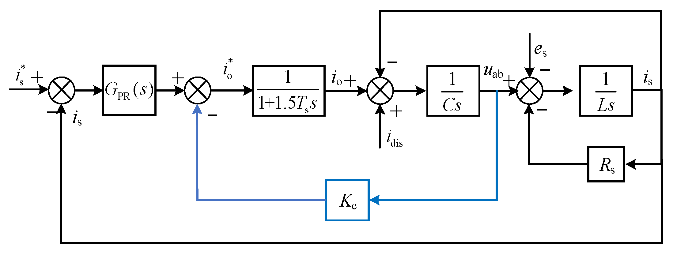
5. Grid Current Control Scheme Based on Capacitor Voltage Feedback

Compared with the VSI with an LCL-type third-order filter, the CSI has an LC second-order filter on the grid side, and the resonance peak phenomenon still exists in its Bode plot. When the line inductance increases as a result of changes in grid impedance and inductive load connection, the resonant frequency point shifts to low frequency, causing more serious low-frequency resonance, resulting in the oscillation during the system dynamic adjustment process. Therefore, before designing the controller parameters, the active damping needs to be introduced to effectively suppress the LC resonance.

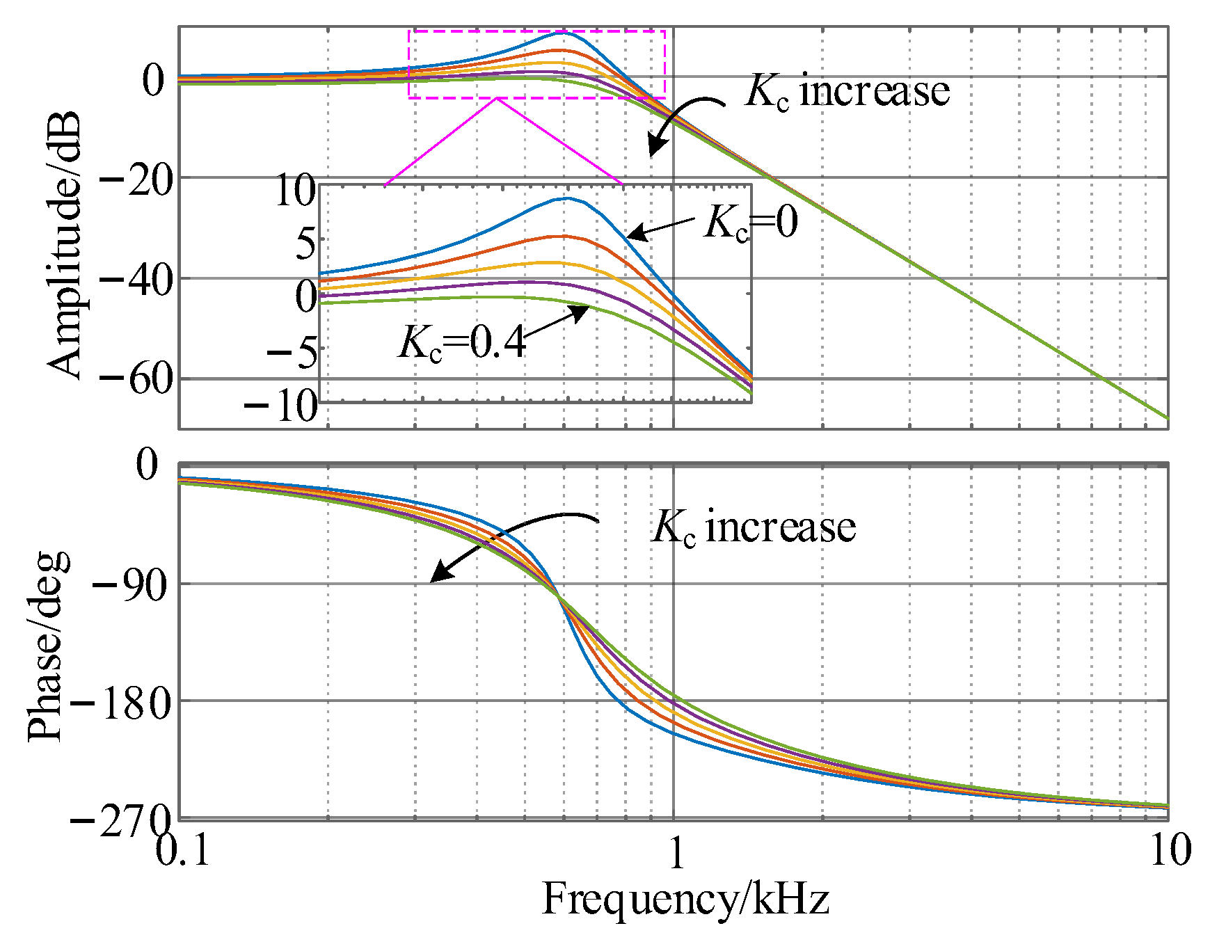
5.1. Active Damping Based on Voltage Feedback

The transfer function Gio2is(s) from io to is is derived as follows:
G io 2 is ( s ) = i s ( s ) i o ( s ) = 1 L s C s 2 + R s C s + 1
Rs is the line loss and the impedance is very small, so Gio2is(s) is a second underdamped state, and a resonance peak occurs in its Bode plots. Since the capacitor voltage is easy to sample, the active damping method based on the feedback of uab is adopted in this paper. Firstly, a mathematical model in the s-domain of the AC-side control system is constructed, which is shown in Figure 8.
The sampling and digital delay are combined [23], and are equivalent to the first-order transfer function T(s); its expression is as follows:
T ( s ) = 1 1 + 1.5 T s s
where Ts is the sample and carrier period. When the capacitor voltage feedback is introduced to the control loop, the transfer function of Gio2is(s) is re-expressed as follows:
G io 2 is ( s ) = 1 L ( 1.5 T s + C ) s 2 + ( 1 . 5 T s R + C R + K c L ) s + K c R + 1
Substituting the parameter values, as shown in Table 1 into Equation (16), the amplitude–frequency characteristic curves of Gio2is(s) can be obtained for different values of the capacitor voltage feedback coefficient Kc, as shown in Figure 9. In all frequency bands, changes in Kc have no effect on Gio2is(s), the resonance spikes of Gio2is(s) gradually decrease with the increase in Kc, and the gains at the resonance frequencies are all less than 0 dB under Kc > 0.3. Nevertheless, with the increase in Kc, the gain of the low band will also decrease slightly. When Kc is too large, the inverter needs to output io with a larger amplitude to generate the same grid-side current. However, the DC-side inductor current is limited, and excessive Kc will cause overmodulation, resulting in the amplitude error of grid current, so Kc is set as 0.3.

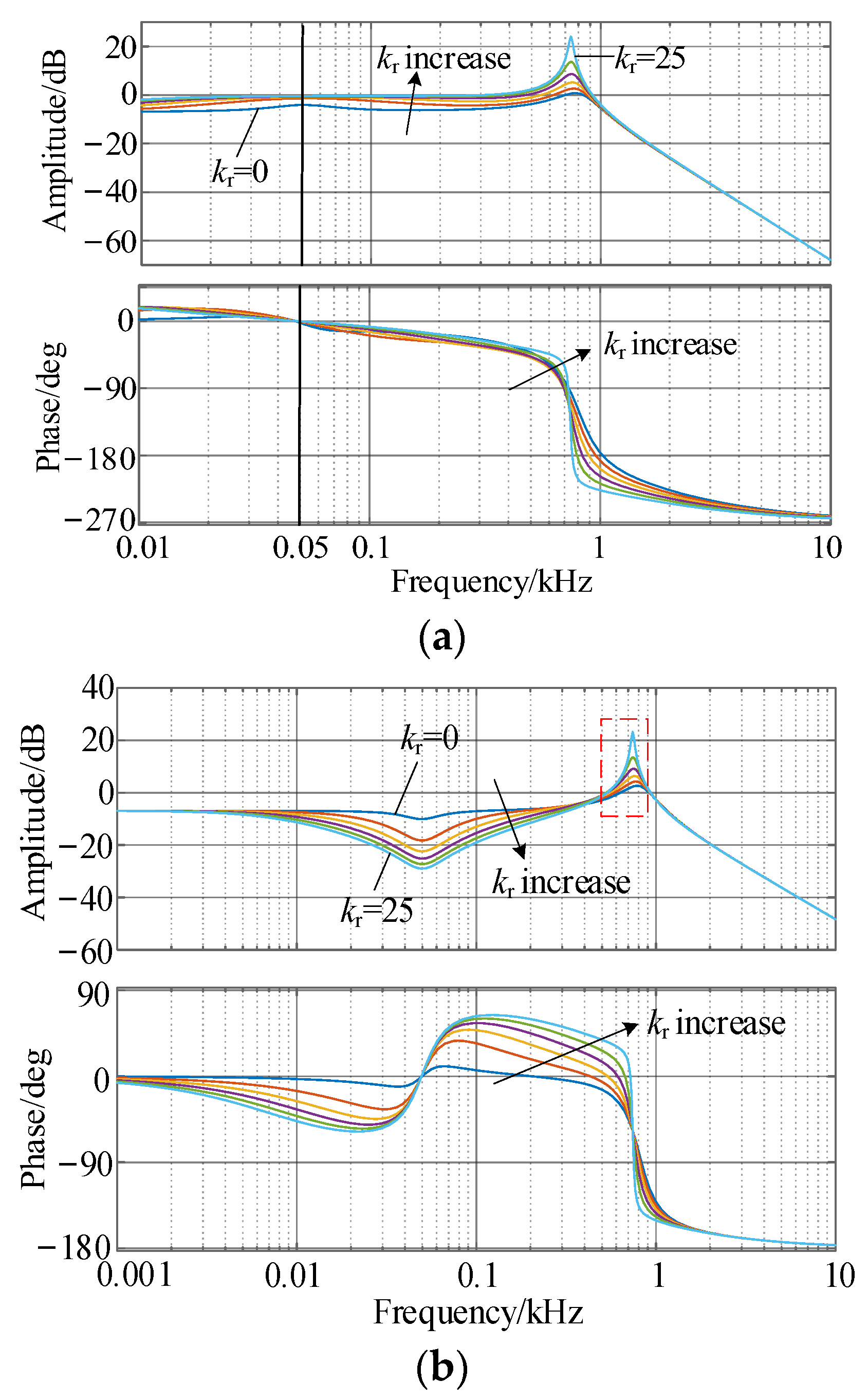
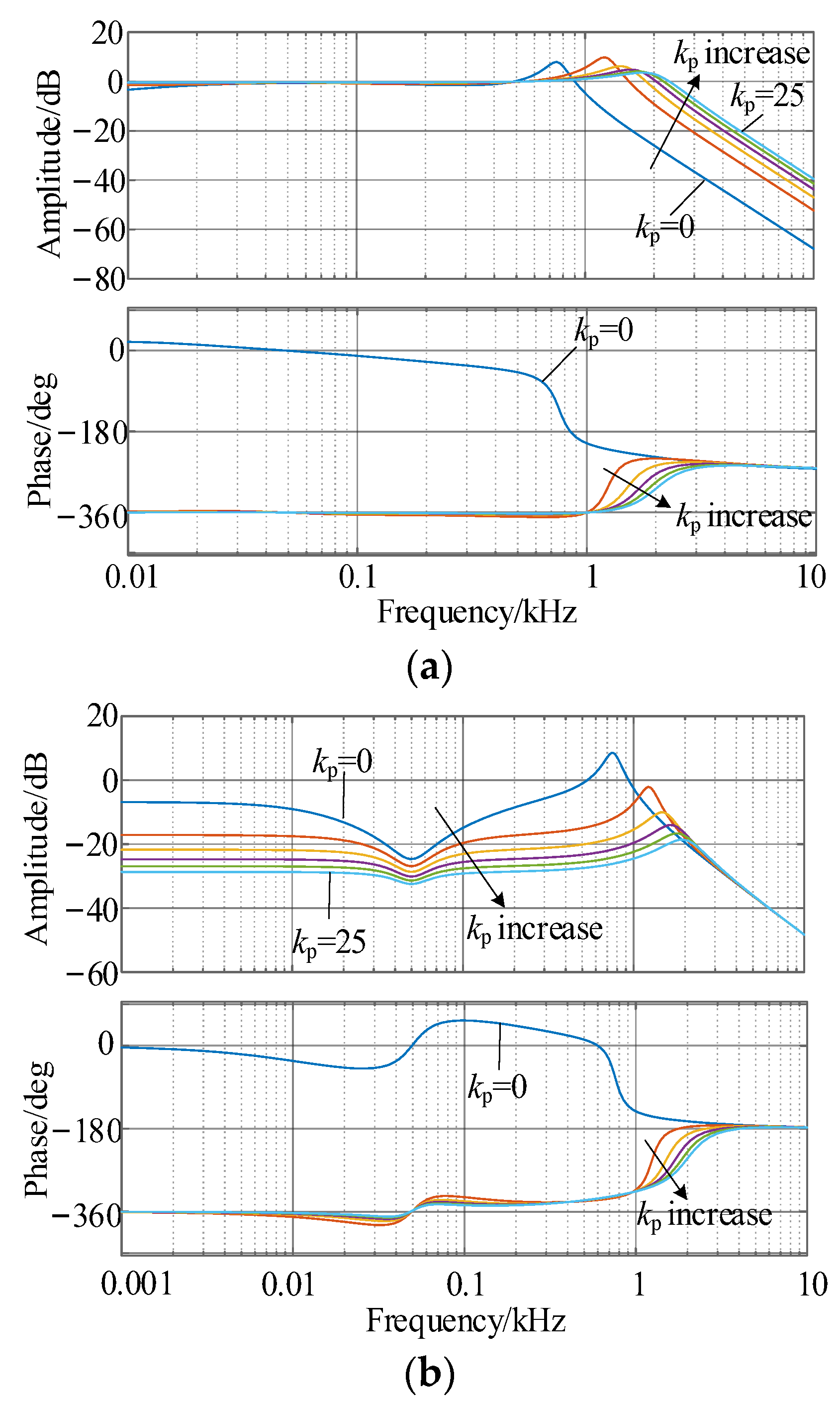
5.2. Controller Parameter Design Method

For the single-phase system, since only one AC component cannot be mapped to DC component by the Park transformation, the PI control algorithm in the rotating coordinate system cannot be applied [20]. Reference [11] proposed a method of constructing orthogonal imaginary axis components to achieve conversion from AC to DC systems, but this will increase the execution time of the program and reduce the robustness of the system. Therefore, in this paper, a proportional resonance (PR) controller GPR(s) is adopted to realize a single closed-loop control of is, and the transfer function of GPR(s) is shown as follows:
G PR ( s ) = k p + 2 k c ζ ω 0 s s 2 + 2 ζ ω 0 s + ω 0 2
where kp is the proportional coefficient, kc is the resonance coefficient, and ζ is the resonance damping, which is set as 0.5 in this paper. ω0 is the angular frequency and is equal to 100π. The open-loop transfer function Gopen(s) can be expressed as follows:
G open ( s ) = G PR ( s ) T ( s ) G io 2 is ( s )
The closed-loop transfer function Gclose(s) can be expressed as follows:
G close ( s ) = G open ( s ) 1 + G open ( s )
During the modulation process, io has abundant sideband harmonics at the carrier frequency and its multiples. It is also necessary to delay the turn-off signal to prevent the DC-side inductor current from breaking, resulting in the presence of 5th, 7th, 11th, and 13th harmonic components in io. In the modeling process, the low and high harmonics are equated to the disturbance current idis in Figure 5, and the transfer function Gidis2is(s) from idis to is can be derived as follows:
G idis 2 is ( s ) = G io 2 is ( s ) 1 + G open ( s )
Subsequently, the individual impacts of kp and kr on the performance of the control system are discussed in detail. Firstly, kp is set as 0, and the amplitude–frequency characteristics and phase-frequency characteristic curves of Gclose(s) and Gidis2is(s) under different kr are drawn, as shown in Figure 10a,b. As kr increases, Gclose(s) gradually approaches the 0 dB line in the low-frequency band, and is and ia remain in the same phase at 50 Hz. In the high-frequency band, kr has no effect on Gclose(s). However, in Figure 10b, it can be seen that in the frequency band from 500 Hz to 950 Hz, Gidis2is(s) produces a large spike as kr increases. It will amplify the perturbing effect of the 11th and 13th harmonics in idis on is.
Next, kr is set as 15, and the amplitude–frequency characteristics and phase-frequency characteristic curves of Gclose(s) and Gidis2is(s) under different kp are drawn, as shown in Figure 11a,b. In the low-frequency band, kp has little effect on Gclose(s), while in the high-frequency band, the cutoff frequency of Gclose(s) increases with the increase in kp. But when kp > 10, the cutoff frequency is 2 kHz, and the sensitivity to kp becomes smaller. In Figure 11b, the amplitude–frequency characteristic curve of Gidis2is(s) gradually decreases with the increase in kp, and when kp > 5, the amplitude gain of Gidis2is(s) is lower than 0 dB in the whole frequency band, which means that the control system is capable of attenuating all the harmonics generated by the modulation process.
Combining the above analysis, the parameters of the PR controller in this paper are set as kp = 10 and kr = 5.

6. Simulink Results and Analysis

The simulation model of the proposed topology, modulation, and control scheme are established in the Matlab2021b/Simulink environment, and the Simulink parameters are listed in Table 1. The correctness of the calculation method for the DC-side inductor current and the effectiveness of the hysteresis loop control strategy are simulated and verified. The reference amplitude of is is set as 10 A, and the parameters shown in Table 1 are substituted into Equation (11) to obtain the optimal value of i dc * of 14 A. The simulation is carried out for this case, and the simulated waveforms of is and idc, as well as the results of the FFT analysis of is, are shown in Figure 12a. To show that i dc * = 14 A is in the optimal range, simulation is carried out for the two cases of i dc * = 12.5 A and i dc * = 15.5 A, and the simulation waveforms are shown in Figure 12b,c. The three sets of simulation results shown in Figure 10 indicate that the idc can accurately follow i dc * , so the effectiveness of the DC-side inductor current hysteresis loop control strategy proposed in Section 3.2 has been verified. When i dc * = 12.5 A, the amplitude of is is only 9.85 A, which is lower than the reference amplitude of 10 A, and there are obvious low harmonic distortions. When i dc * = 15.5 A, is has no steady-state error, but the third harmonic component and THD are greater than those under i dc * = 14 A. The above simulation results can prove the correctness of the calculation method for the reference of the DC-side inductor current.
The effectiveness of the active damping method based on the capacitor voltage feedback is simulated and verified, the simulation is also carried out under the operating condition of i dc * = 14 A, and the reference amplitude of is is set as 10 A. For the capacitive voltage feedback channel not introduced, the simulation waveform of is is shown in Figure 13a, and it can be seen that there is an obvious current ripple in is. For the capacitor voltage feedback coefficient Kc set as 0.5, the simulation waveform is shown in Figure 13b. Although there is no obvious harmonic distortion, the amplitude of is is only 8.6 A. Comparing the two aspects of control performance and power quality, the simulation results under Kc = 0.3, shown in Figure 13a, are better than those under Kc = 0 and Kc = 0.5, which indicates the feasibility of the transfer function derivation and capacitor voltage feedback coefficient determination methods.

7. Experimental Results and Analysis

As shown in Figure 14, a grid-connected CSI experimental platform is established. The TMS320F28335 (TEXAS Instruments, Dallas, TX, USA) is used to execute the control algorithm and generate the switching signals, the switching tube and diode models are FF100R12RT4 (Infineon, Neubiberg, Germany) and MEK75-12DA (Infineon, Neubiberg, Germany), and other passive device parameters and carrier frequency are consistent with Table 1.

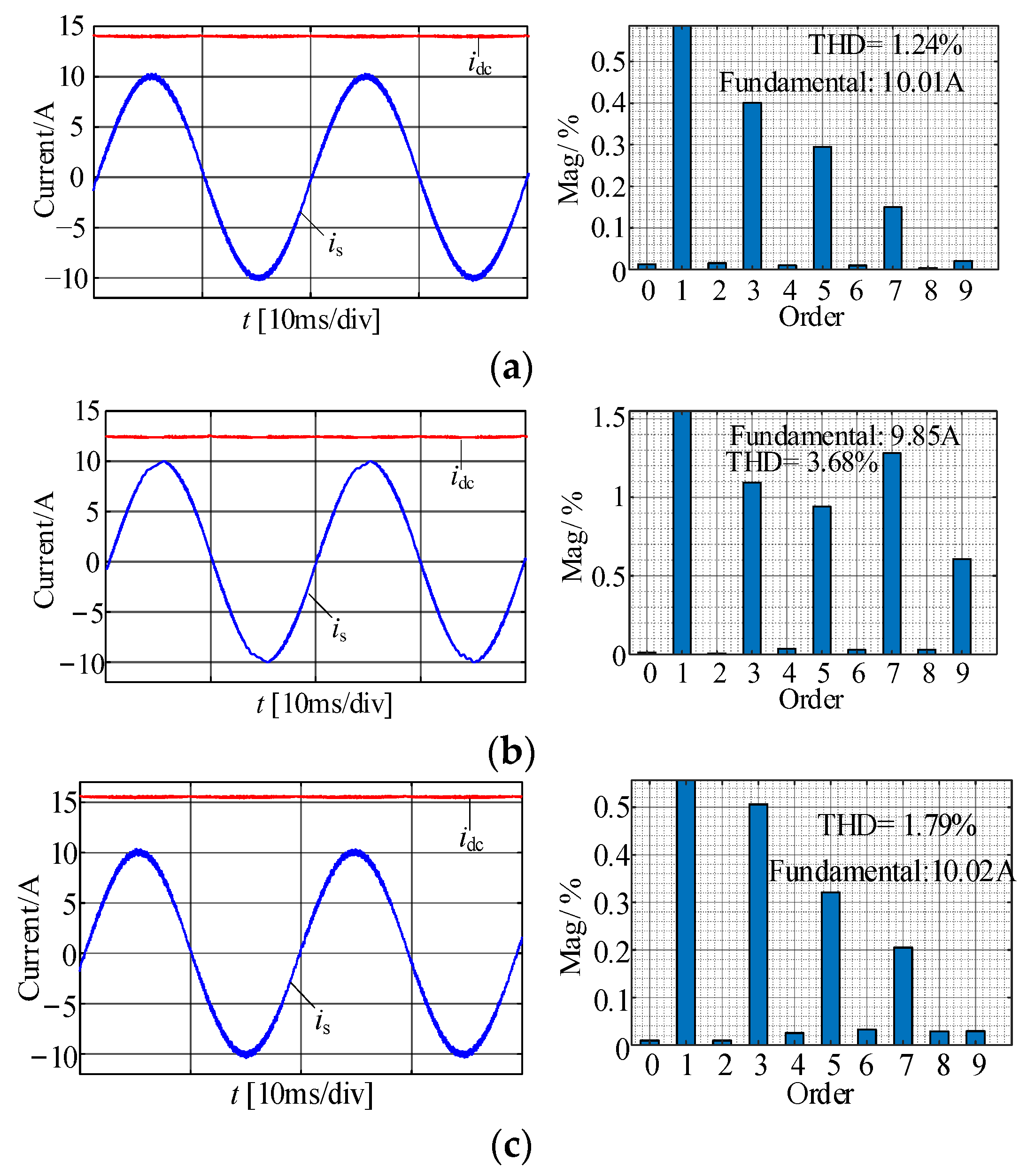
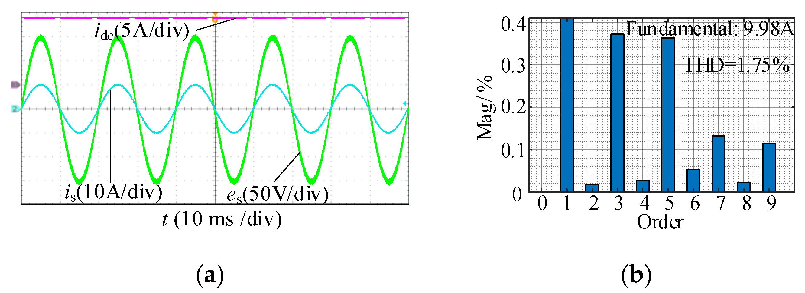
7.1. Steady-State Verification

The experimental verification is firstly carried out in the boost mode, where udc is regulated to 100 V and the programmable grid simulator outputs an AC voltage with a frequency of 50 Hz and an amplitude of 150 V. Similar to the simulation, the reference amplitude of is is set as 10 A and the phase is synchronized with the grid voltage. Substituting into Equation (10) yields i dc * = 14 A. Under the proposed DC-side inductor current hysteresis controller and the PR controller of the grid current, the steady-state experimental waveforms are shown in Figure 15a, and the results of the FFT analysis are shown in Figure 15b. The CSI maintains the unit power factor operation without steady-state error, and the content of each low-order harmonic is within 0.4%, while the idc is capable of accurately tracking the reference.
Next, udc is increased to 270 V, and the system operates in the buck mode. i dc * is set as 11.3 A. The steady-state experimental waveforms are shown in Figure 16a, and the FFT analysis results are shown in Figure 16b, the excellent steady-state performance and power output quality can be obtained, which shows that the DC-side inductor current control and modulation scheme proposed for the five switches single-phase CSI is correct and feasible, while solving the inherent defect of traditional CSI that cannot operate in buck mode.

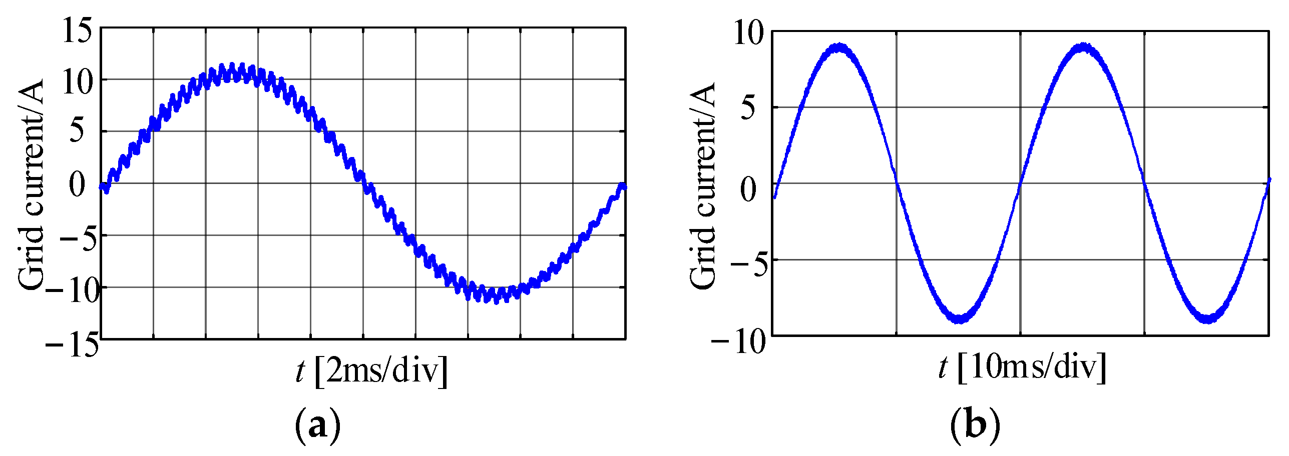
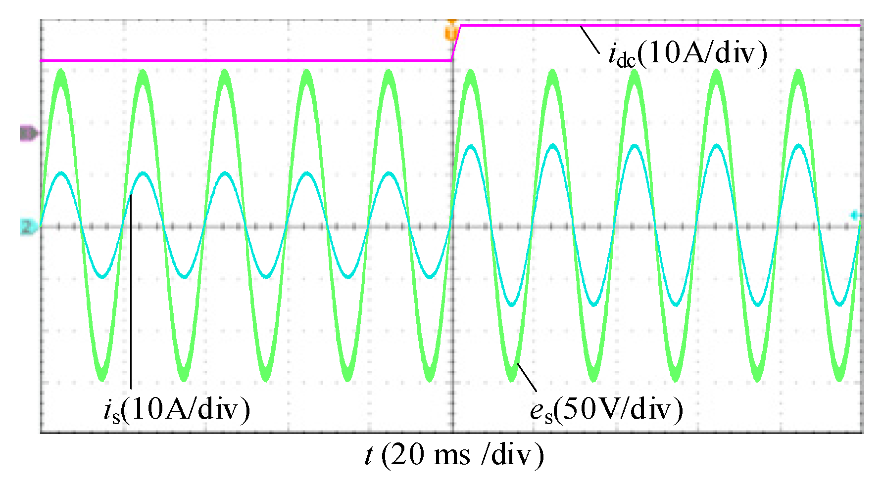
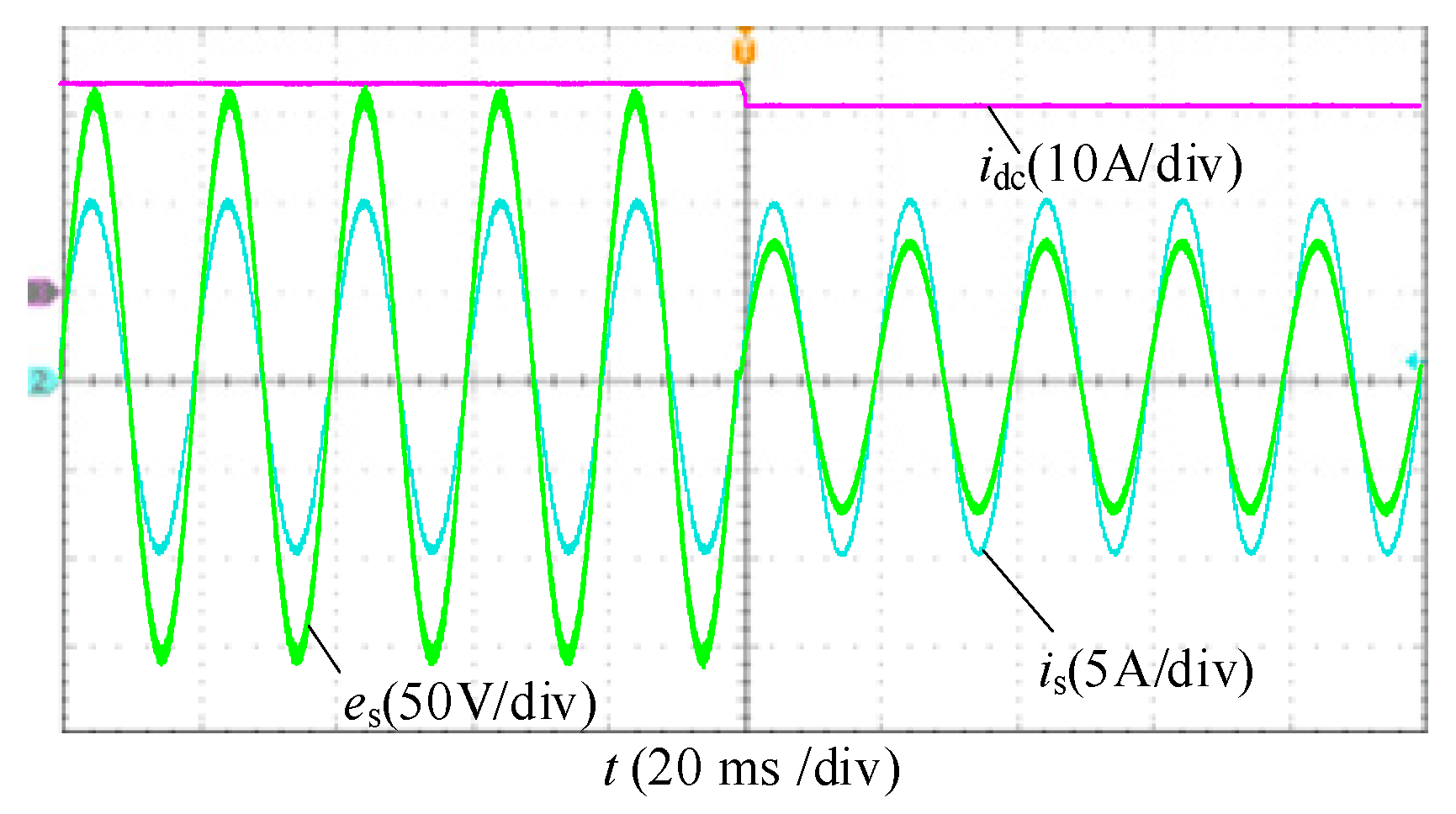
7.2. Dynamic Verification

The CSI operates in boost operation, and the reference amplitude of is is adjusted from 10 A to 15 A, and i dc * is set from 14 A to 20.8 A according to Equation (11). The dynamic experimental waveforms of this process are shown in Figure 17. idc restores to the steady state after 3 ms, and there is no steady-state error and overshoot. Due to the short dynamic adjustment process of idc, it can provide sufficient current output for the grid side. Under the adjustment of the designed PR controller, is can track the reference within half a cycle and remain in the same phase with es.
The amplitude of the grid voltage decreases from 160 V to 80 V, the CSI operates from boost mode to buck mode, and the reference amplitude of the grid current is still 10 A. According to the calculation method for the DC-side inductor current under different operation modes in Section 3.1, i dc * should be reduced from 13.6 A to 10.6 A. The experimental waveforms are shown in Figure 18. idc quickly drops to the reference, and under the effect of the PR controller, the amplitude of is is restored to 10 A immediately. The experimental results show that a good dynamic performance can be obtained by the DC-side inductor current hysteresis loop controller and the grid current PR controller designed in this paper.

8. Conclusions

To solve the problem that the DC-side inductor current is not stable and controlled in the traditional topology of a CSI, a novel single-phase CSI topology with five switching tubes was taken as the research object. The calculation for the reference of the DC-side inductor current, the modulation scheme for the single-phase CSI, and the optimal parameters design method of the proportional-resonance controller based on the feedback capacitor voltage were proposed in this paper. Finally, the simulation and experimental results were tested for the proposed CSI topology to validate the effectiveness of the proposed control and modulation scheme. The main conclusions of this paper are included below:
(1)
The control method of the DC-side inductor current is proposed in this paper, which can give the DC side the characteristics of the controlled current source. Hence, it can realize the independent control of the DC side and the AC grid side, improving the reliability and practicality of the CSI.
(2)
Based on output current polarity, the proposed logic conversion method can convert the PWM signals into switching signals of the single-phase CSI; there is no need to add hardware logic circuits.
(3)
The proposed active damping method based on the feedback capacitor voltage can effectively suppress the resonance peak caused by the LC filter on the grid side.
(4)
The optimization design of the PR controller is analyzed in this paper. The results show that increasing the resonance coefficient can eliminate the steady-state error, and the suppression ability of the harmonic components can be improved by increasing the proportional coefficient.

Author Contributions

Conceptualization, T.F. and J.G.; methodology, H.L.; software, B.X.; validation, T.F., J.G. and H.L.; formal analysis, B.X.; investigation, T.F.; resources, J.G.; data curation, T.F.; writing—original draft preparation, J.G.; writing—review and editing, T.F.; visualization, J.G.; supervision, H.L.; project administration, B.X.; funding acquisition, T.F. All authors have read and agreed to the published version of the manuscript.

Funding

This work was supported in part by the Education Department of Henan Province under Grant 2024SJGLX0924, in part by the science and technology research project of Henan Province under Grant 242102210022, and in part by Education Department of Henan Province under Grant 24B510015.

Data Availability Statement

The original contributions presented in the study are included in thearticle; further inquiries can be directed to the corresponding author.

Conflicts of Interest

The authors declare no conflicts of interest.

References

  1. Mahdavi, M.; Jurado, F.; Schmitt, K.; Chamana, M. Electricity Generation from Cow Manure Compared to Wind and Photovoltaic Electric Power Considering Load Uncertainty and Renewable Generation Variability. IEEE Trans. Ind. Appl. 2024, 60, 3543–3553. [Google Scholar] [CrossRef]
  2. Xia, B.; Huang, S.; Zhang, J.; Zhang, W.; Liao, W.; Gao, J.; Wu, X. An Improved High-Frequency Voltage Signal Injection-based Sensorless Control of IPMSM Drives with Current Observer. IEEE Trans. Transp. Electrif. 2023, 1. [Google Scholar] [CrossRef]
  3. Wang, W.; Gao, F.; Yang, Y.; Blaabjerg, F. An Eight-Switch Five-Level Current Source Inverter. IEEE Trans. Power Electron. 2019, 34, 8389–8404. [Google Scholar] [CrossRef]
  4. Dong, Z.; Wen, H.; Song, Z.; Liu, C. 3-D SVM for Three-Phase Open-End Winding Drives with Common DC Bus. IEEE Trans. Power Electron. 2023, 38, 9340–9346. [Google Scholar] [CrossRef]
  5. Liu, J.; Yang, M.; Wang, T. Impedance-Based Stability Analysis of Grid-Tied Photovoltaic System with Superconducting Magnetic Energy Storage System. IEEE Trans. Appl. Supercond. 2021, 31, 5402504. [Google Scholar] [CrossRef]
  6. Pan, D.; Ruan, X.; Bao, C.; Li, W.; Wang, X. Magnetic Integration of the LCL Filter in Grid-Connected Inverters. IEEE Trans. Power Electron. 2014, 29, 1573–1578. [Google Scholar] [CrossRef]
  7. Guo, W.; Chen, T.; Huang, A.Q. A Control Bandwidth Optimized Active Damping Scheme for LC and LCL Filter-Based Converters. IEEE Access 2023, 11, 34286–34296. [Google Scholar] [CrossRef]
  8. Rajeev, M.; Agarwal, V. Single phase current source inverter with multiloop control for transformer less grid–PV interface. IEEE Trans. Ind. Appl. 2018, 54, 2416–2424. [Google Scholar] [CrossRef]
  9. Guo, X.; Sui, S.; Wang, B.; Zhang, W. A current-based approach for short-circuit fault diagnosis in closed-loop current source inverter. IEEE Trans. Ind. Electron. 2019, 67, 7941–7950. [Google Scholar] [CrossRef]
  10. Geng, Y.; Yun, Y.; Chen, R.; Wang, K.; Bai, H.; Wu, X. Parameters Design and Optimization for LC-Type Off-Grid Inverters with Inductor-Current Feedback Active Damping. IEEE Trans. Power Electron. 2018, 33, 703–715. [Google Scholar] [CrossRef]
  11. Migliazza, G.; Buticchi, G.; Carfagna, E.; Lorenzani, E.; Madonna, V.; Giangrande, P.; Galea, M. DC current control for a single-stage current source inverter in motor drive application. IEEE Trans. Power Electron. 2020, 36, 3367–3376. [Google Scholar] [CrossRef]
  12. Titus, J.; Harikrishnan, P.; Hatua, K. An SCR-Based CSI-Fed Induction Motor Drive for High Power Medium Voltage Applications. IEEE Trans. Ind. Electron. 2021, 68, 4657–4666. [Google Scholar] [CrossRef]
  13. Yang, S.; Peng, F.Z.; Lei, Q.; Inoshita, R.; Qian, Z. Current-fed quasi-Z-source inverter with voltage Buck–Boost and regeneration capability. IEEE Trans. Ind. Appl. 2010, 47, 882–892. [Google Scholar] [CrossRef]
  14. Li, Y.W.; Pande, M.; Zargari, N.R.; Wu, B. DC side inductor current minimization for high-power current-source motor drives. IEEE Trans. Power Electron. 2008, 24, 232–240. [Google Scholar]
  15. Zhang, D.; Wang, P.L.; Wang, L.Q.; Zhu, W.T. Three-phase Sepic-type current source inverter that can suppress common mode current. Acta Energiae Solaris Sin. 2023, 44, 266–273. [Google Scholar]
  16. Guo, X.; Wang, N.; Zhang, J.; Wang, B.; Nguyen, M.-K. A novel transformerless current source inverter for leakage current reduction. IEEE Access 2019, 7, 50681–50690. [Google Scholar] [CrossRef]
  17. Wang, W.; Gao, F.; Yang, Y.; Blaabjerg, F. Operation and modulation of H7 current-source inverter with hybrid SiC and Si semiconductor switches. IEEE J. Emerg. Sel. Top. Power Electron. 2017, 6, 387–399. [Google Scholar] [CrossRef]
  18. Miao, Y.; Liao, W.; Huang, S.; Liu, P.; Wu, X.; Song, P.; Li, G. DC side inductor Current Minimization Scheme for IM Drive System Fed by Bidirectional DC Chopper-Based CSI. IEEE Trans. Transp. Electrif. 2023, 9, 2839–2850. [Google Scholar] [CrossRef]
  19. Zhang, Y.; Yang, T.; Miao, Y.R. Research on the Modulation and Control Strategy for a Novel Single-Phase Current Source Inverter. Energies 2023, 16, 6729. [Google Scholar] [CrossRef]
  20. Kiran, V.; Rajeevan, P.P. A New Carrier Based Modulation Technique for Current Source Inverters. In Proceedings of the 2020 IEEE International Conference on Power Electronics, Smart Grid and Renewable Energy (PESGRE2020), Cochin, India, 2–4 January 2020. [Google Scholar]
  21. Song, P.Y.; Liu, Y.H.; Liu, C. Research on Parameter Design and Control Method for Current Source Inverter–Fed IM Drive Systems. Machines 2022, 10, 922. [Google Scholar] [CrossRef]
  22. Guo, Q.; Zhou, C.L.; Li, S. A Multiple Loops Control Strategy Based on DC Link Voltage of Current Source PWM Rectifiers. Trans. China Electrotech. Soc. 2022, 37, 2051–2063. [Google Scholar]
  23. Xia, B.; Huang, S.; Zhang, J.; Zhang, W.; Liao, W.; Huang, X.; Huang, S. Encoderless Deadbeat Predictive Current Control for SPMSM Drives with Online Parameter Identification. IEEE Trans. Transp. Electrif. 2024, 1. [Google Scholar] [CrossRef]
Figure 1. The topology of the traditional single-phase CSI.
Energies 17 03640 g001
Figure 2. Simulation waveforms of DC-side inductor current and load current for traditional CSI. (a) Initial value of idc is zero; (b) initial value of idc is 20 A.
Energies 17 03640 g002aEnergies 17 03640 g002b
Figure 3. Several improved topologies of CSI. (a) Quasi-Z source, (b) additional switching tube parallel with inductor, (c) buck–boost, (d) two-transistor forward voltage–current converter.
Energies 17 03640 g003
Figure 4. Topology of the proposed single-phase grid-connected CSI with five switching tubes.
Energies 17 03640 g004
Figure 5. Vector diagram of the AC side in CSI.
Energies 17 03640 g005
Figure 6. Hysteresis control block diagram of idc.
Energies 17 03640 g006
Figure 7. Diagram of switching signals. (a) X = 1; (b) X = 0.
Energies 17 03640 g007
Figure 8. Closed-loop control diagram of grid current.
Energies 17 03640 g008
Figure 9. Bode plots of Gio2is(s) under different Kc.
Energies 17 03640 g009
Figure 10. Bode plots of Gclose(s) and Gidis2is(s) under different kr. (a) Gclose(s); (b) Gidis2is(s).
Energies 17 03640 g010
Figure 11. Bode plots of Gclose(s) and Gidis2is(s) under different kp. (a) Gclose(s); (b) Gidis2is(s).
Energies 17 03640 g011
Figure 12. Simulation results under different references of DC-side inductor current. (a) i dc * = 14 A; (b) i dc * = 12.5 A; (c) i dc * = 15.5 A.
Energies 17 03640 g012
Figure 13. Simulation results under different capacitor voltage feedback coefficients. (a) Kc = 0; (b) Kc = 0.5.
Energies 17 03640 g013
Figure 14. The experimental platform of grid-connected CSI.
Energies 17 03640 g014
Figure 15. Experimental results in boost mode. (a) Waveforms; (b) FFT analysis results.
Energies 17 03640 g015
Figure 16. Experimental results in buck mode. (a) Waveforms; (b) FFT analysis results.
Energies 17 03640 g016
Figure 17. Dynamic experimental waveforms under the change in the reference amplitude for grid current.
Energies 17 03640 g017
Figure 18. Dynamic experimental waveforms under the change in the operating mode.
Energies 17 03640 g018
Table 1. Parameters of CSI.
ParametersValue
DC input voltage udc (V)270
DC-side inductance Ldc (mH)4
Amplitude of grid voltage es (V)311
Filter capacitance C (µF)12
Inductance L (mH)0.5
Resistance R (Ω)0.5
Frequency f (kHz)10
Disclaimer/Publisher’s Note: The statements, opinions and data contained in all publications are solely those of the individual author(s) and contributor(s) and not of MDPI and/or the editor(s). MDPI and/or the editor(s) disclaim responsibility for any injury to people or property resulting from any ideas, methods, instructions or products referred to in the content.

