Article

Adaptive Fast Integral Terminal Sliding Mode Control Strategy Based on Four-Switch Buck–Boost Converters

1
College of Electronic Engineering, Xi’an University of Posts and Telecommunications, Xi’an 710121, China
2
College of Computer Science, Xi’an University of Posts and Telecommunications, Xi’an 710121, China
*
Author to whom correspondence should be addressed.
Energies 2024, 17(15), 3645; https://doi.org/10.3390/en17153645
Submission received: 20 May 2024 / Revised: 18 July 2024 / Accepted: 20 July 2024 / Published: 24 July 2024

Abstract

:
With the rapid development of electronic power systems, DC-DC converters are widely used, including the Four-Switch Buck–Boost (FSBB) converter, which has a unique advantage in scenarios with a wide range of voltage inputs. To improve the response speed and anti-interference capability of the FSBB converter, this paper proposes an adaptive global fast integral terminal sliding mode control method. Through an in-depth analysis of the fundamental characteristics of the FSBB converter, this study employed a global fast integral terminal sliding mode controller combined with an adaptive algorithm to significantly improve the dynamic performance and robustness of the FSBB converter. The simulation and experimental results show that the proposed method could track the reference voltage quickly and accurately in different modes, exhibiting excellent system robustness compared to conventional sliding mode control, terminal sliding mode control, and PID control methods.

1. Introduction

With the rapid development of power electronics, the demand for DC-DC converters is increasing in various applications [1,2]. DC-DC converters have been widely used in multiple integrated power systems [3,4], such as photovoltaic and wind power generation [5] and super-capacitor and battery power management in hybrid vehicles [6], electric cars [7], and DC microgrid systems [8] due to their low cost, simple structure, and high power efficiency. However, as the application requirements increase, the limitations of conventional DC-DC converters in terms of efficiency, dynamic response, and stability are gradually becoming apparent.
The traditional DC-DC converter is challenging to drive due to the high number of passive components and the opposite polarity of the input and output, which significantly affect the converter’s efficiency. The Four-Switch Buck–Boost (FSBB) converter [9] addresses these issues with its nonlinear characteristics, simple structure, low voltage stress on the switching components, identical input and output polarity, fewer passive components, and wide input voltage range. These features enhance the system’s efficiency and reliability.
Researchers mainly divide FSBB control strategies into two categories [10,11]. The first is the quadrilateral inductor current control mode [12], which achieves zero-voltage conduction of all switching tubes but produces high switching losses. The second is multi-mode control [13], which is simple to implement and offers high energy transfer efficiency. Multi-mode control methods are subdivided into three-mode, two-mode, and single-mode control, with the converter selecting the appropriate mode of operation by comparing the input and output voltages. The research objectives for FSBB [14] include achieving smooth mode switching and optimal conversion efficiency. To optimize mode switching, researchers typically rely on multi-mode control, focusing on the overall control design to improve both the steady-state and dynamic responses of the system. For efficiency optimization, they generally employ hard-switching and soft-switching control modes [15] to minimize converter losses.
Intelligent algorithms such as PID [16], sliding mode control [17], and fuzzy logic control [18] are widely incorporated in nonlinear systems to prevent environmental factors from affecting the systems’ performance. The FSBB converter also requires the design of an effective control method. Cai, J. et al. [19] proposed a control method that combines PID control with bipolar double-zero compensation applied to the FSBB controller. This method improves the system’s dynamic responses and steady-state accuracy. Komurcugil, H. et al. [20] proposed an FSBB-based Lyapunov function control strategy that employs independent control equations for the two modes. This strategy avoids the mode detection process while enabling smooth mode switching. To facilitate good transient performance and smooth mode switching, Ullah, Q. et al. [21] proposed sliding mode control based on FSBB, which ensures that the FSBB converter can accurately track the output voltage in different operating modes and achieve smooth transitions between them. This proves the feasibility of the sliding mode control method applied to the FSBB converter.
The sliding mode variable structure control method is characterized by structural versatility, control discretization, and system nonlinearity, allowing it to quickly adapt to different operating conditions while ensuring system stability and performance. Tan, S.C. et al. [22] proposed a sliding mode control method with fixed-frequency PWM. The experimental results show that this method can track the reference voltage under large loads and linear disturbances. To improve the steady-state performance, Ardhenta, L. et al. [23] proposed a Buck-converter-based PI-SMC controller to enhance the Buck converter’s accuracy. To mitigate the effects of parameter uncertainty, studies [24,25] have adjusted the switching gain in real time to reduce jitter by combining sliding mode control with an adaptive algorithm. Liu, P. et al. [26] introduced an adaptive discrete sliding mode control method for a Buck converter, which improves the tracking accuracy using a discrete disturbance observer. Zambrano-Prada, D. et al. [27] proposed adaptive sliding mode control for a Boost converter. They combined the switching term of sliding mode control with an adaptive algorithm by tracking the integral of the output voltage error, resulting in a system with a short settling time and good steady-state performance. Linares-Flores et al. [28] proposed an adaptive sliding mode control method that combines a hyperbolic tangent function with an extended state observer and applies them to a Buck–Boost converter to suppress jitter. However, this approach sacrifices some system robustness.
Chang, Y. et al. [29] proposed applying non-vector-terminated sliding mode control to the Boost converter to improve the algorithm’s convergence speed. Based on this, an extended state observer [30] was introduced to further reduce the system jitter and improve the system’s robustness and response speed. Liu, Z. et al. [31] proposed the application of fixed-time, observer-based, non-singular terminal sliding mode control to a Buck converter, which employs a new second-order, fixed-time convergence law to improve the system’s immunity to disturbances. The tracking performance of the output voltage is further enhanced [32] using a continuous, non-singular terminal sliding mode control based on a finite-time disturbance observer. To further improve the convergence speed, Malge, S.V. et al. [33] proposed a global non-singular, fast terminal sliding mode control, which effectively enhances the system’s stability in the face of disturbances and enables fast dynamic responses and stable steady-state performance. To enable the system to converge in a finite time, Kaifei, Z. et al. [34] proposed a fast integral terminal sliding mode control method applied to permanent magnet synchronous motors. This method solves the problems of the terminal sliding mode’s singularity and the integral sliding mode’s inability to converge in a finite time and effectively improves the system’s dynamic characteristics.
Table 1 provides a summary analysis of the above literature. The current multi-mode control strategies applied to FSBB converters use mainly PID algorithm control and traditional sliding mode control, which renders the system error unable to complete the convergence in a limited time. The control performance and system stability are affected when encountering unknown disturbances or parameter uncertainty. To address the above problems, this paper proposes combining the global fast integrating terminal sliding mode control with an adaptive algorithm to design an adaptive global fast integrating terminal sliding mode control (ATSMC) to obtain a faster response speed and stronger system robustness. The simulation and experimental results show that this control method can significantly improve the response speed and steady-state performance while achieving smooth mode switching.

2. Working Principle and Modeling of FSBB

2.1. Operational Principle

The FSBB converter is formed by cascading Buck and Boost circuits, as shown in Figure 1. The left bridge arms Q1 and Q2 are the components of the Buck circuit. Q1 is the main controller, with a duty cycle of d1. Q2 is complementary to Q1 and has a duty cycle of 1 – d1. The right bridge arms Q3 and Q4 form the Boost circuit. Q4 is the main controller, with a duty cycle of d2, while Q3 and Q4 are complementary. Q3 has a duty cycle of 1 – d2. According to the principle of volt-second balance, the input–output relationship of FSBB is as follows:
M = V o V i = d 1 1 d 2
Equation (1) shows that the converter’s voltage ratio is related to d1 and d2, and d1 and d2 are independent of each other. The design expectation is to obtain a stable output voltage over a wide input voltage range.

2.2. Modeling Analysis

The output voltage is lower than the input voltage for the Buck mode. In a steady-state control condition, Q1 = d1, and Q3 is normally open. Figure 2 shows one cycle of operation in the Buck mode. In Figure 2a, the input voltage source to the inductor-charging IL increases, and in Figure 2b, the inductor to the load-discharging IL decreases. The combination of the two can be used to obtain the Buck circuit, and the KCL, the KVL, and the principle of volt-second balance can be obtained with the following differential equations:
d I L dt = 1 L ( d 1 V i   V o )
d V o dt = 1 C ( I L   V o R )
The Boost mode is used when the input voltage is lower than the output voltage. In a steady-state control condition, Q4 = d2, and Q2 is normally off. Figure 3 shows one cycle of operation in the Boost mode. In Figure 3a, the inductor and the power-supply-discharging IL decrease at the same time. In Figure 3b, the capacitor is discharged through the load. The combination of the two can be used to obtain the Boost circuit, and the following differential equations can be obtained from the KCL, KVL, and volt–second equilibrium:
d I L dt = V o 1 d 2 L + V i L
d V o dt = I L 1 d 2 C     V o RC

3. Controller Design

3.1. Buck Mode

The voltage tracking error is defined as follows:
e = x 1 x ref
where x1 is the output voltage and xref is the reference voltage. By combining Equation (6) with Equations (2) and (3), the derivative of the voltage error (x2) can be obtained as follows:
x 2 = e ˙ = x 1 ˙ = 1 C ( I L V o R )
Commonly used sliding mode controllers typically use linear sliding mode surfaces:
s t ( t ) = e t ˙ + λ e ( t )
where λ is a positive constant. Assuming that there is a time t, which makes St converge to zero, we can obtain e(t) = e (0)eλt. When e (0) is not infinite, the error e(t) converges to infinity, but this reduces the dynamic performance of the controller. Therefore, in this paper, a global fast integrating terminal sliding mode surface is used:
s = e ˙ + λ 1 e + λ 2   0 t e p q ( τ ) d τ
In this equation, λ1 and λ2 are constants called sliding mode coefficients, which determine the decay rate of the tracking error, while p and q are positive odd numbers that satisfy 1 < p/q < 2. This sliding mode surface ensures that the voltage error converges to zero in a finite time, resulting in voltage stabilization in a finite time. When the voltage error converges completely, s = 0. Based on Equation (9), we can obtain
e ˙ + λ 1 e + λ 2   0 t e p q ( τ ) d τ = 0
which can be collated to obtain
e 1 ¨ = λ 1 e 1 ˙ λ 2   e 1 p q
where e 1 = 0 t e ( τ ) d τ . Further simplification yields
e 1 ˙ d e 1 ˙ = λ 1 e 1 ˙ λ 2   e 1 p q d e 1
Integrating both sides of the above equation yields:
0 e 1 ( 0 ) ˙ e 1 ˙ d e 1 ˙ = 0 e 1 ( 0 ) λ 1 e 1 ˙ λ 2   e 1 p q d e 1
Assuming that the time for the voltage error to converge to zero is Ts and the initial value of the error is bounded and non-zero, i.e., e1(0) is bounded, solving Equation (13) yields
0 T s λ 2 e 1 2 ˙ dt = 0.5 λ 1 e 1 2 ˙ 0 + q λ 3 p + q e 1 p + q q ( 0 )
Then, the voltage error convergence time (Ts) is
T s = λ 1 e 2 0 / [ 0.5 e 2 0 + q λ 2 p + q e 1 p + q q ( 0 ) ]
Since the initial value of the voltage error is bounded and non-zero, the convergence time is also bounded, i.e., the voltage error satisfies finite-time convergence. The convergence time is adjusted by adjusting the sliding mode parameters. By combining Equation (9) and Equations (2) and (3), the global fast integrating terminal sliding mode control law is obtained as follows:
u eq = CL V i [ λ 2 e p q λ 1 x 2 1 CR x 2 + x 1 CL ]
where ueq is the equivalent control quantity when the system works on the sliding mode surface. When the system does not operate on the sliding mode surface, it is necessary to add switching control on this basis. The switching control equation is
u sw = CL V i ksign ( s )
where k is a constant, and the duty cycle output for the Buck mode is
u = u eq + u sw = CL V i [ λ 2 e p q λ 1 x 2 1 CR x 2 + x 1 CL + ksign ( s ) ]
Equation (18) is the control law for the Buck mode, and the output u is the duty cycle, i.e., d1. However, in practical applications, there are often unknown external disturbances.
s ˙ = λ 1 e ˙ + e ¨ + λ 2   e p q + w ( z )
w(z) is defined as the set of all disturbances, including input disturbances, load disturbances, and external disturbances, which need to be corrected using the control law:
u = u eq + u asw
Ueq is the same as Equation (16), and uasw is an adaptive control input designed as follows:
u asw = CL V i k ^ sign ( s )
where k ^ is the adaptive gain, a is the adaptive gain, and it is assumed that there is a positive real number (kd) such that u asw = CL V i k d sign s is the final, i.e., steady-state, value of uasw. Kd must satisfy the following condition:
kd > w(z)
The adaptive gain derivative of the design is
k ^ ˙ = η | s |
where η is called the adaptive gain coefficient and η > 0, which determines the convergence speed of k ^ when the value of η is reasonable. k ^ can obtain the steady-state value before the system reaches the sliding mode so as not to affect the steady-state performance of the system.
The purpose of the global fast adaptive integral terminal sliding mode is mainly to make the system function converge to zero in a finite time so that the system can obtain the estimated value of the disturbance boundary ( k ^ ), enhance its robustness, and achieve a fast and accurate response. Next, the stability of the controller is verified.
The adaptive gain error is defined as follows:
k ~ = k ^ k d
The Lyapunov function derivative is
V ˙ = s s   ˙ + 1 η k ~ k ~ ˙ = s w z   - k ^ sign s + k ^ - k d s sign ( s ) = s × w z   k d | s | < 0
Equation (22) shows that the controller is stable for a finite time and that the sliding variables converge to zero in a finite time, which satisfies the stability requirement.

3.2. Boost Mode

Since the Boost mode of FSBB has the characteristics of a non-minimum phase system, the voltage error cannot be tracked directly. For this paper, we chose the system’s energy storage during the operation as the tracking target to control the voltage indirectly. Since the output voltage is equal to the capacitor voltage, we obtained Equation (26):
y = 1 2 C V o 2 + 1 2 L I L 2
When the system reaches the steady state, the stored energy (y) converges to the reference value (yref). The inductor current and output voltage also converge to the reference current and reference voltage. At the same time, the output voltage, the inductor current, and the system’s stored energy are constant, and the reference inductor current can be obtained from the reference voltage:
I Lref = V ref 2 V i R
The energy storage error is defined as follows:
e = y - y ref
where yref is the reference stored energy. The same global fast integrating terminal sliding mode surface used in the Buck mode is adopted:
s = e ˙ + λ 1 e + λ 2   e p q d t
where λ1 and λ2 are constants called sliding mode coefficients, which determine the decay rate of the tracking error, while p and q are positive odd numbers that satisfy 1 < p/q < 2. This sliding mode surface is demonstrated in Equation (15). It ensures that the error converges to zero and a stable output voltage is achieved in a finite time.
Combining Equations (4), (5), (28), and (29) yields the equivalent control law:
u eq = CRL ( 2 L I i + V i RC ) V o [ λ 2 ( e p q ) + λ 1 V i I i V o 2 R + V i 2 L + 2 V o 2 R 2 C ]
When there is an external disturbance in the system, the derivative of the sliding mode surface function is
s ˙ = λ 2 e ˙ + λ 1 e ¨ + λ 3   e p q + d ( z )
Consistent with the Buck mode, d(z) is the set of all disturbances, including input disturbances, load disturbances, and external disturbances. In order for the system to achieve the sliding mode surface, a switching gain was designed, but a general switching gain is affected by external disturbances, so an adaptive gain was designed as follows:
u asw = CRL 2 L I i + V i RC V o ( η ^ 1 s + η ^ 2 sign ( s ) )
where η ^ 1 and η ^ 2 are adaptive gains. Assuming that η1d and η2d are positive real numbers such that u asw = CRL 2 L I i + V i RC V o ( η 1 d s + η 2 d sign ( s ) ) is the final, i.e., steady-state, value of uasw, η1d and η2d satisfy the following equation:
η1d − η2d < d(Z) < η1d + η2d
The adaptive gain derivatives were designed as follows:
η ^ ˙ 1 = α s
η ^ ˙ 2 = β | s |
where α, β > 0, which determines the convergence speed of η ^ ˙ 1 and η ^ ˙ 2 when the value of α, β is reasonable. η ^ ˙ 1 and η ^ ˙ 2 are able to obtain the steady-state value before the system reaches the sliding mode. Therefore, they do not affect the steady-state performance of the system.
The error of the adaptive gain is defined as follows:
η ~ 1 = η ^ 1 η 1 d
η ~ 2 =   η ^ 2 η 2 d
The derivative of the Lyapunov function was chosen to be
V ˙ = s s   ˙ + 1 α η ~ 1 η ~ ˙ 1 + 1 β η ~ 2 η ~ ˙ 2 = s d z η ^ 1 s η ^ 2 sign ( s ) + ( η ^ 1 η 1 d s ) + η ^ 2 η 2 d s   s i gn ( s ) = s × d z ( η 1 d s + η 2 d s ) < 0
Based on Equation (33), the Lyapunov function is negative and definite, while the Boost mode is asymptotically stable. Meanwhile, the sliding mode function(s) and the adaptive gain error ( η ~ 1   and   η ~ 2 ) converge to zero in a finite time, which satisfies the stability requirement.

4. Simulation Results

The proposed control method was validated via simulation using the MATLAB/Simulink R2022a. The conventional PID control was designed in reference [20], and the conventional sliding mode control (SMC) was designed in reference [22]. The simulation results of these two methods were compared with those of the proposed global fast integral terminal sliding mode control (TSMC) and adaptive global fast integral terminal sliding mode control (ATSMC). In order to cope with sudden load changes that may occur during system operation, the load (R) was designed as shown in Equation (39):
R = V o I o
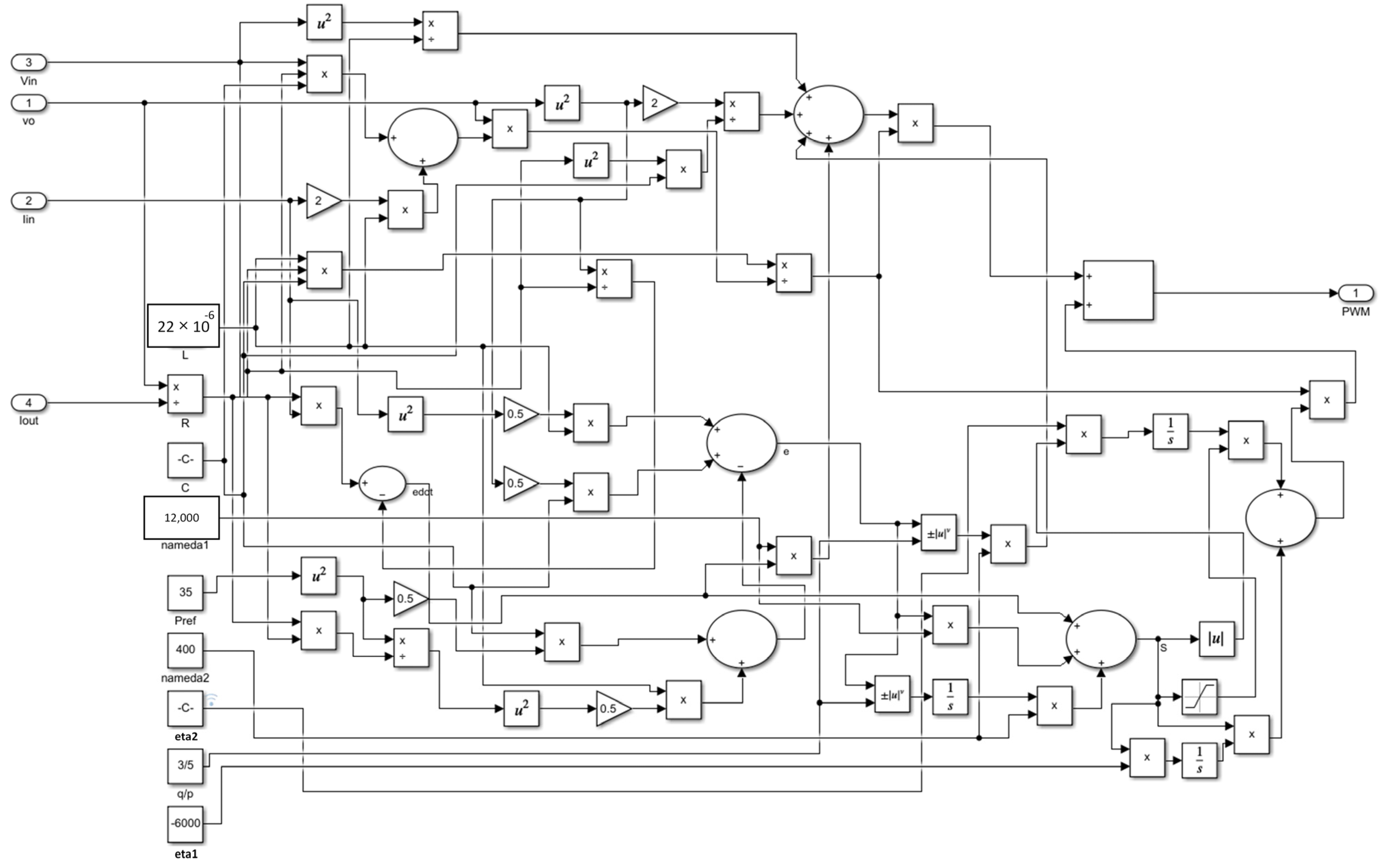
A block diagram of the Boost mode control based on ATSMC is shown in Figure 4 with the following parameters: λ1 = 12,000, λ2 = 4,000,000, η1 = −6000, η2 = –12,000,000, p = 3, and q = 5.
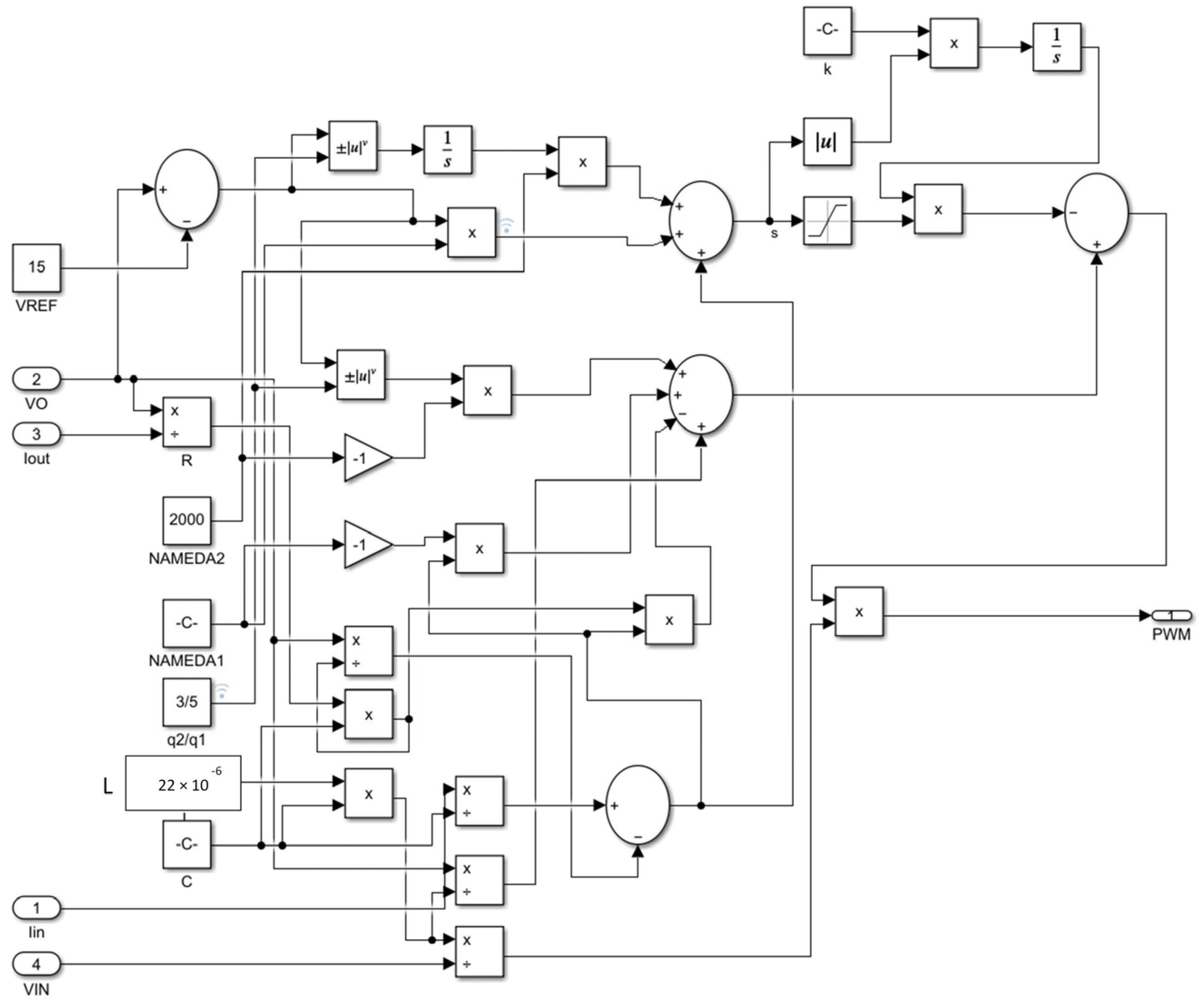
A block diagram of the Buck mode control based on ATSMC is shown in Figure 5 with the following parameters: λ1 = 8,000,000, λ2 = 2000, k = 8,000,000, p = 3, and q = 5.
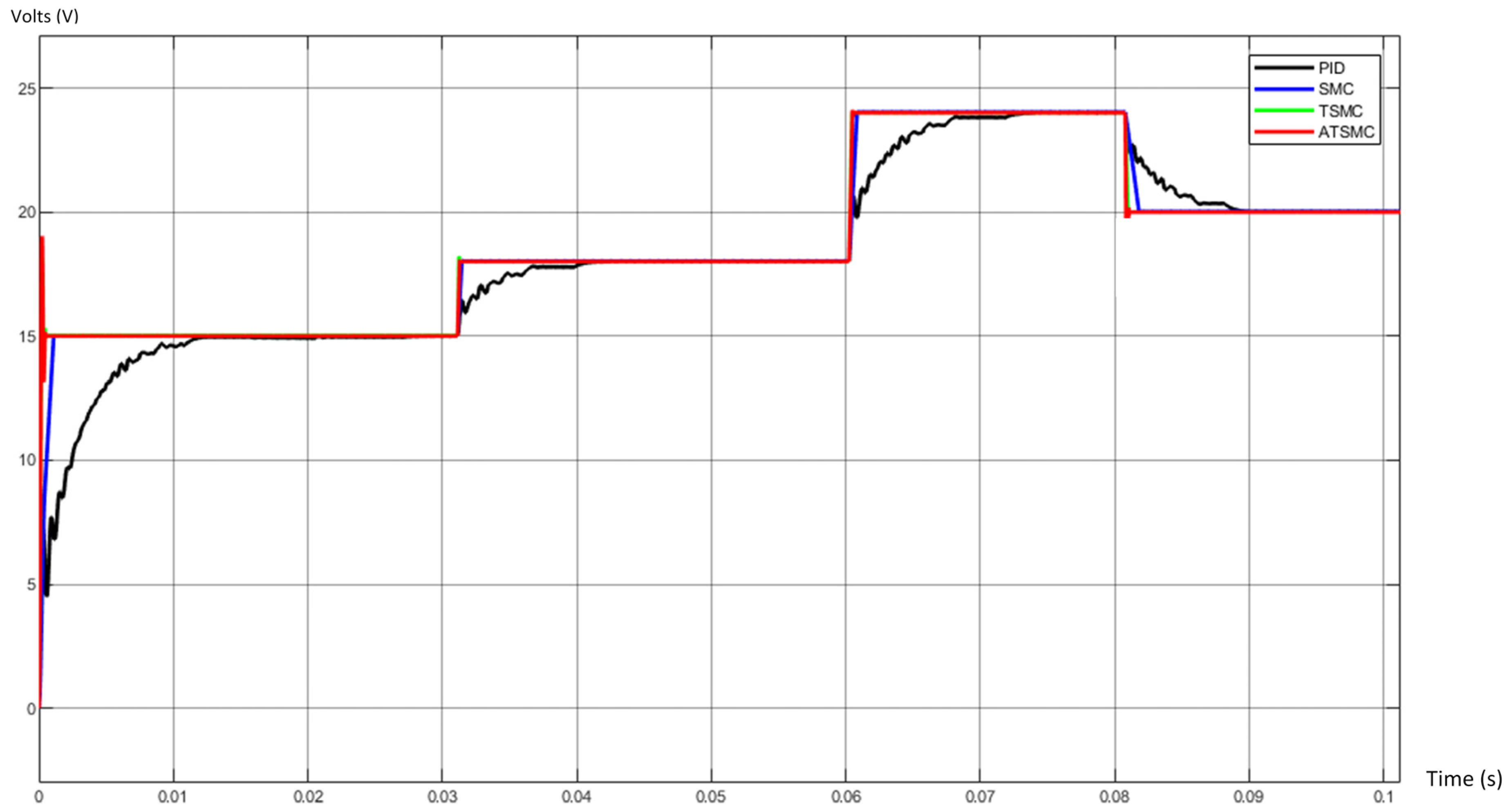
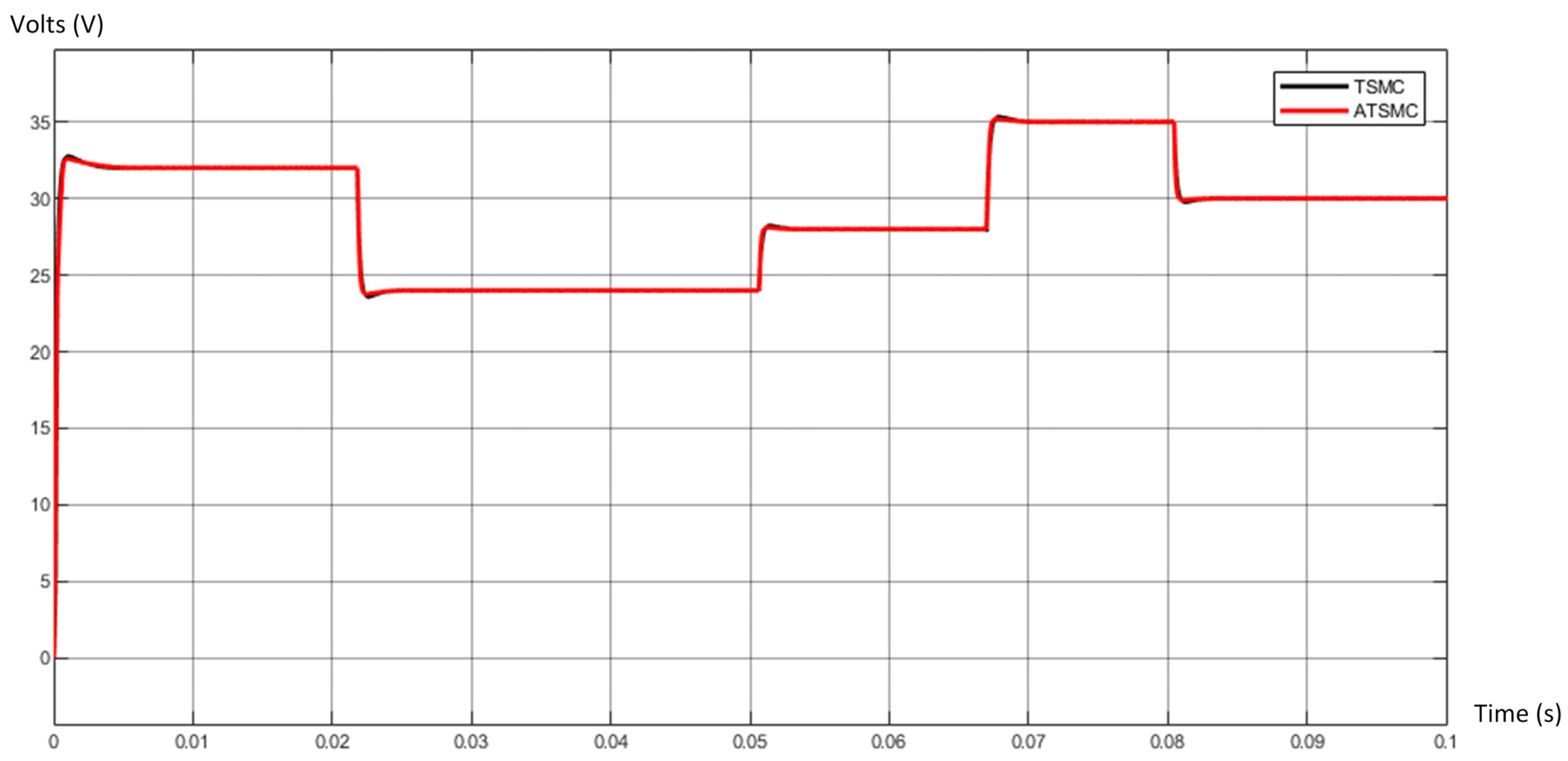
Figure 6 shows the output voltage responses of the four control algorithms in Buck mode. When the reference voltage changed, PID and SMC presented ripples and slow responses, while TSMC and ATSMC could smoothly regulate the voltage to the reference value in a shorter time. Figure 7 shows the output voltage responses of TSMC and ATSMC in Boost mode; both had similar response speeds, but voltage regulation with ATSMC was smoother with less overshoot.
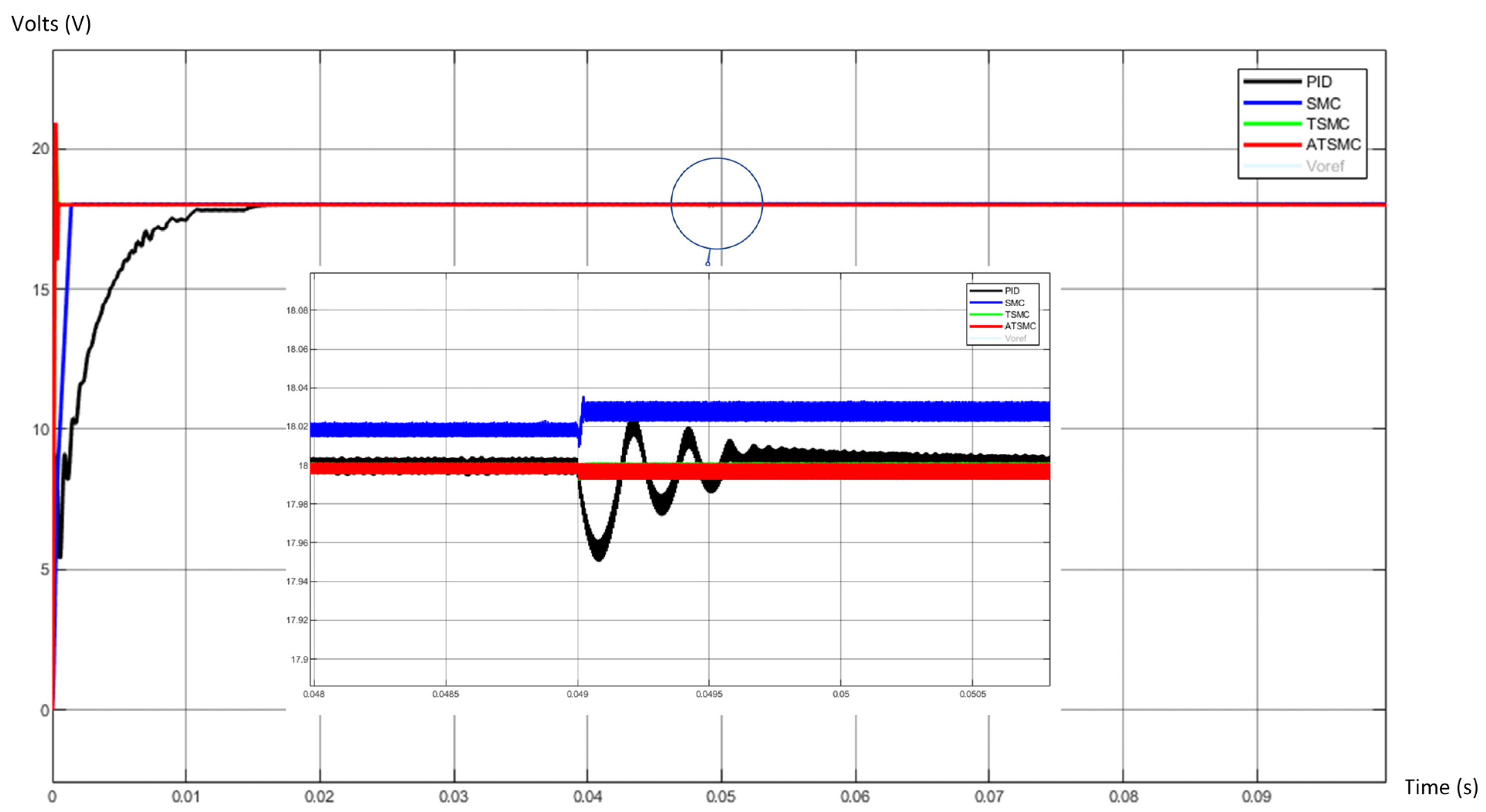
The robustness of the Buck mode load mutation was tested when the input voltage was 30 V, the output voltage was 18 V, and the load resistance was adjusted from 40 Ω to 20 Ω in 0.049 s. The experimental results are shown in Figure 8. The PID had the largest voltage fluctuation and the longest settling time, and the conventional SMC had the largest steady-state error. The TSMC and ATSMC had similar voltage fluctuations, but the ATSMC had less ripple.
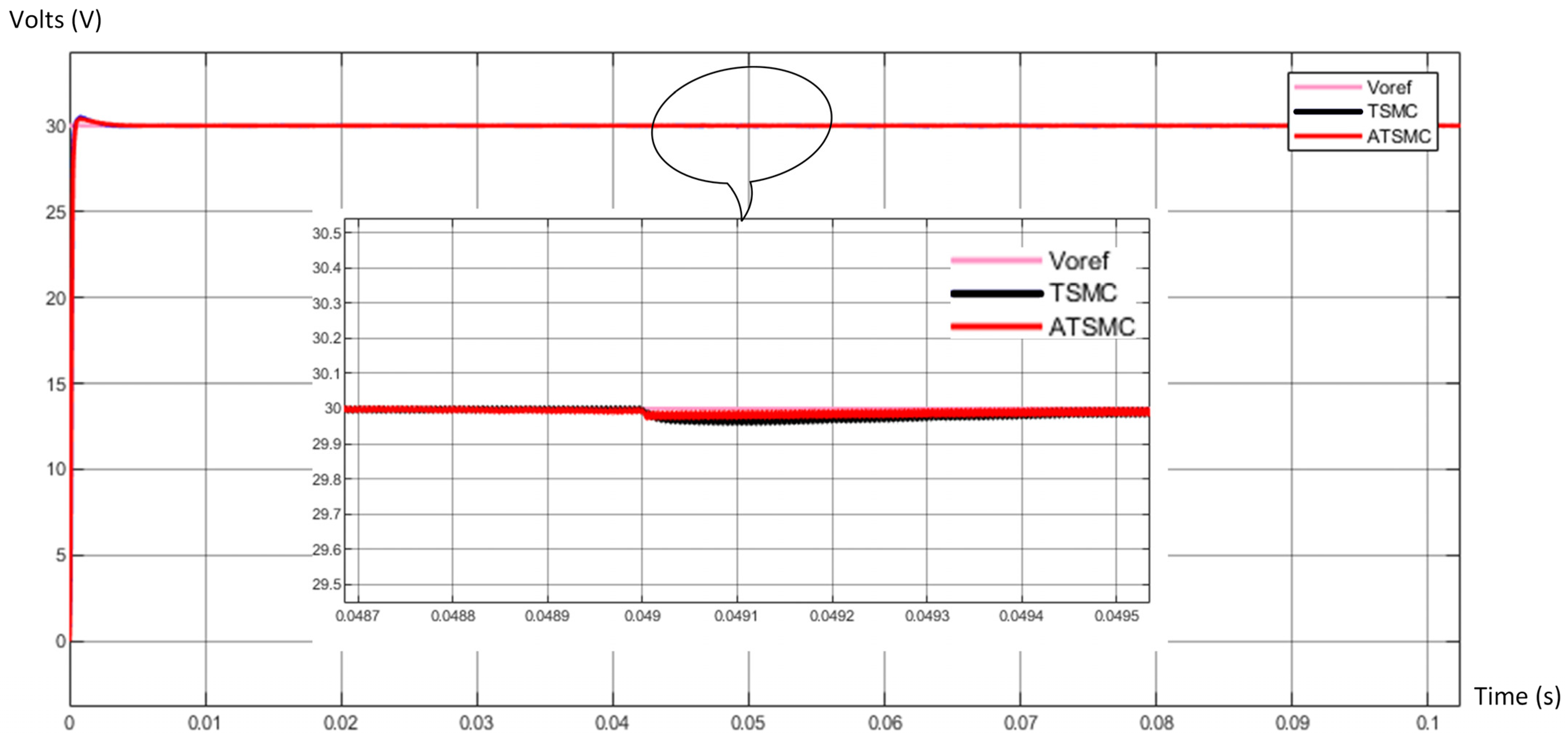
Figure 9 presents the results of a robustness test with a sudden load change in Boost mode at an input voltage of 20 V and an output voltage of 30 V. Again, the load resistance was adjusted from 40 Ω to 20 Ω at 0.049 s. As shown in Figure 9, the TSMC’s voltage fluctuation and settling time were significant, and the ATSMC had the smallest voltage fluctuation and the shortest settling time.
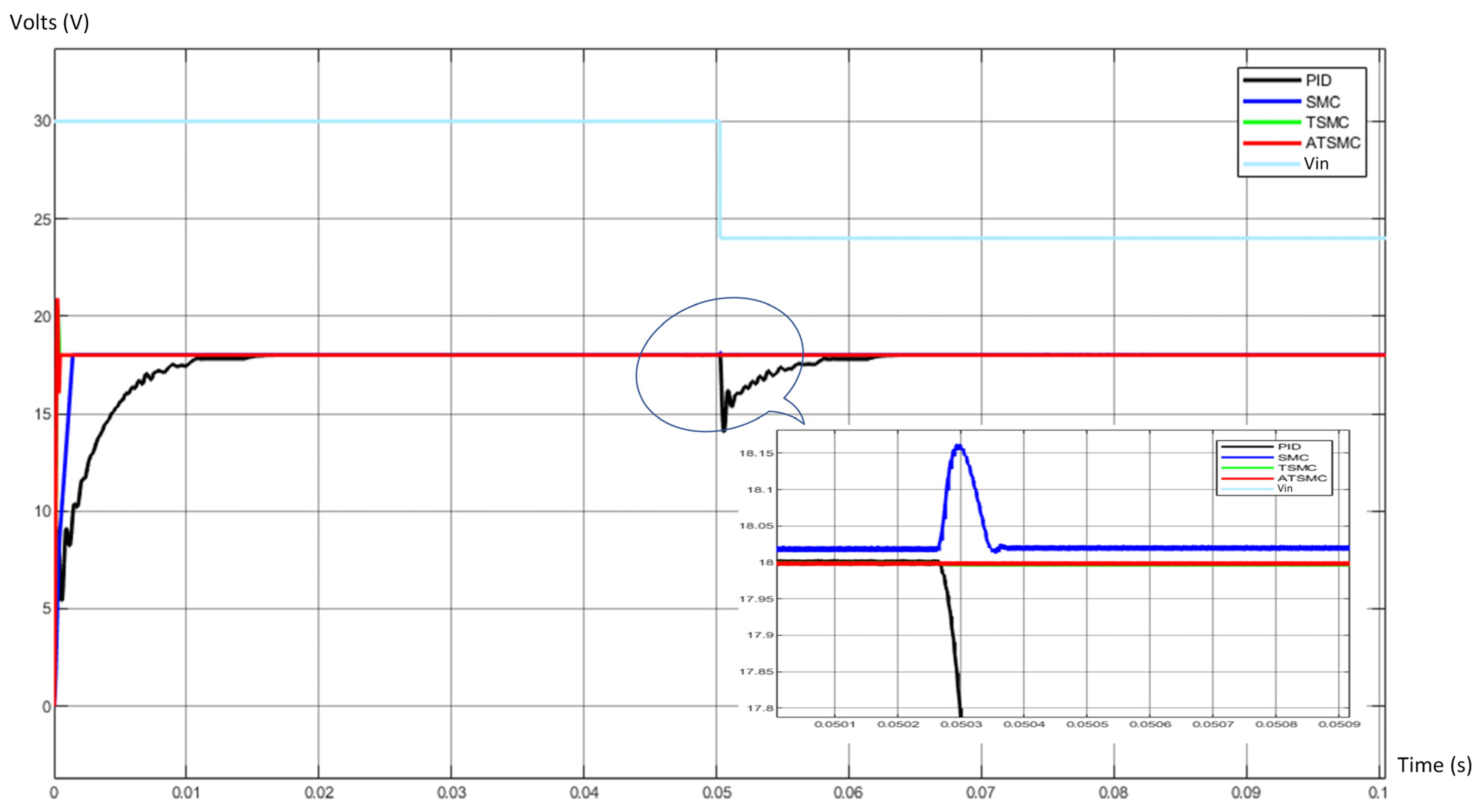
The robustness of the Buck mode input voltage step change was tested. The input voltage was adjusted from 30 V to 24 V in 0.049 s, and the experimental results are shown in Figure 10. It can be seen that the PID had the largest voltage fluctuation and the longest settling time, while the SMC had a large steady-state error and a large overshoot. The TSMC and ASMC had similar voltage fluctuations, but the ATSMC had a shorter settling time.
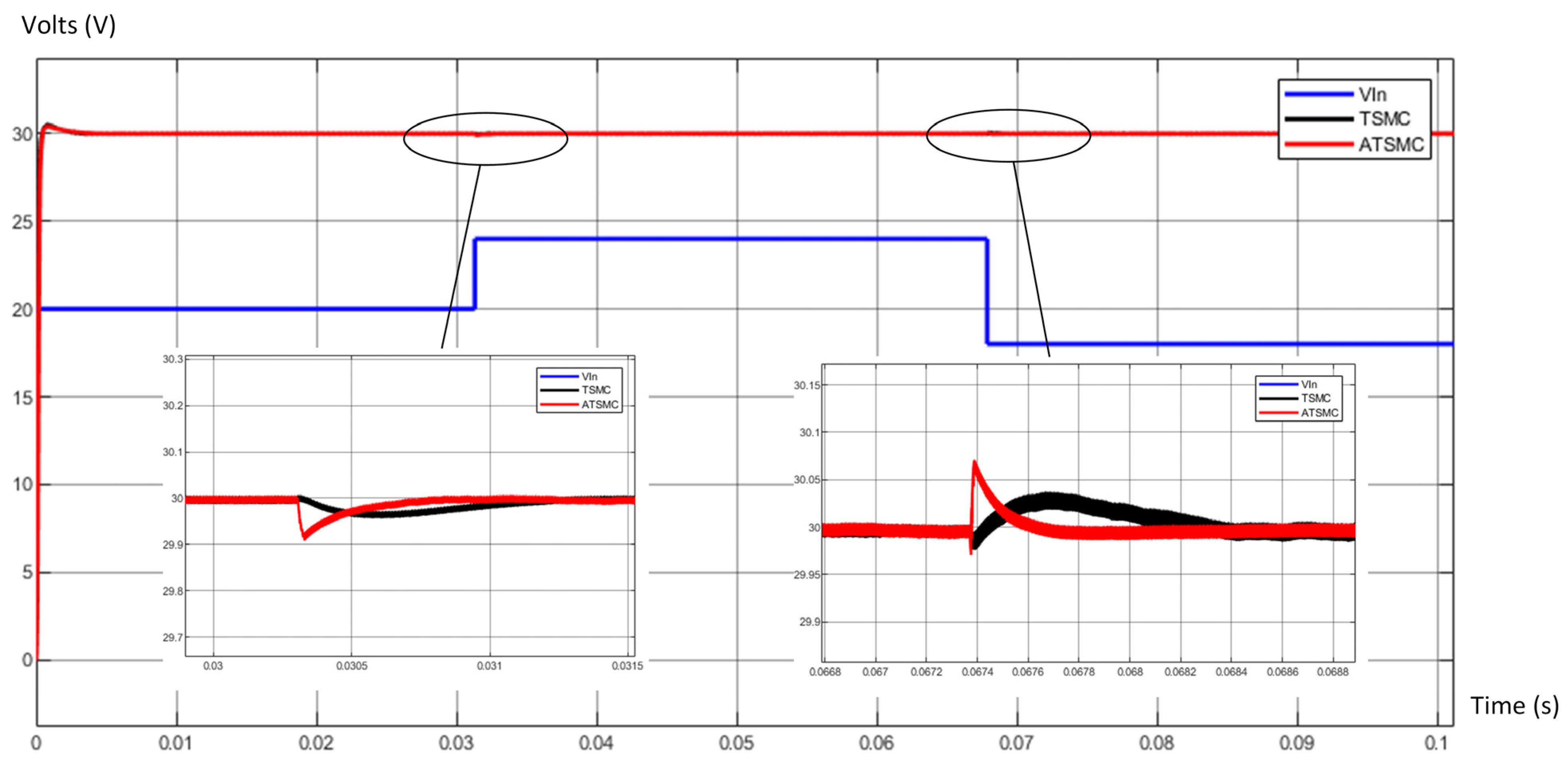
The robustness of the step change in the input voltage in Boost mode was tested by regulating the input voltage from 20 V to 24 V at 0.03 s. Then, it was regulated to 18 V at 0.065 s. The experimental results are shown in Figure 11, which shows that the settling time and ripples of the ATSCM were smaller.
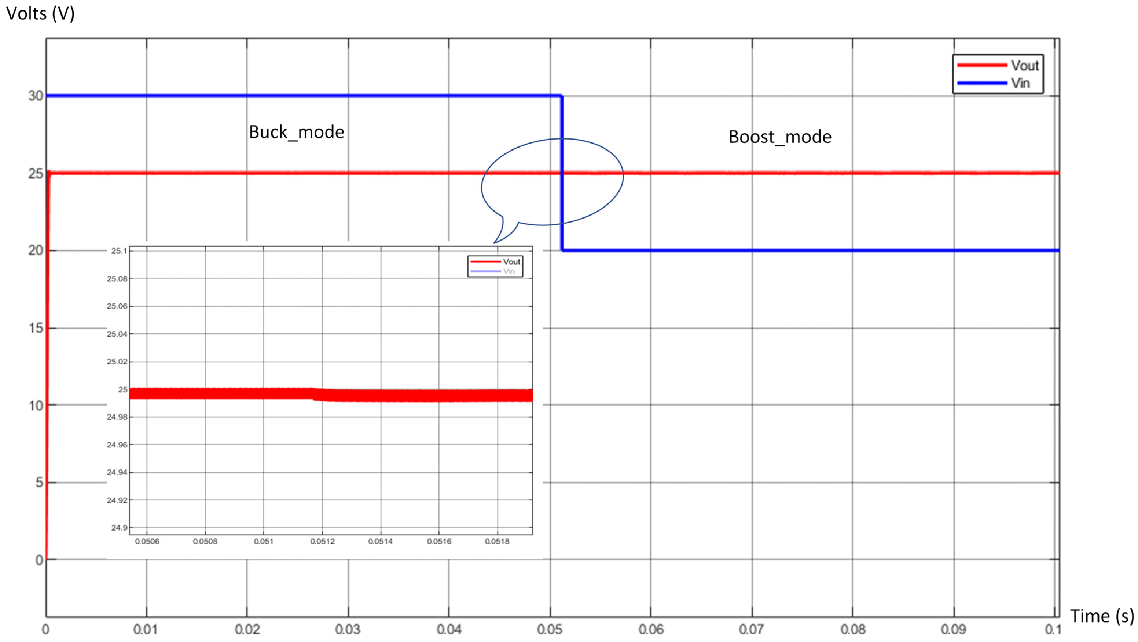
To test the performance of the FSBB converter with the ATSMC algorithm during mode switching, we set the output voltage to a constant 25 V and regulated the input voltage from 30 V to 20 V within 0.05 s. The experimental results are shown in Figure 12. The ATSMC algorithm ensured that the converter remained stable and responded quickly during mode switching.
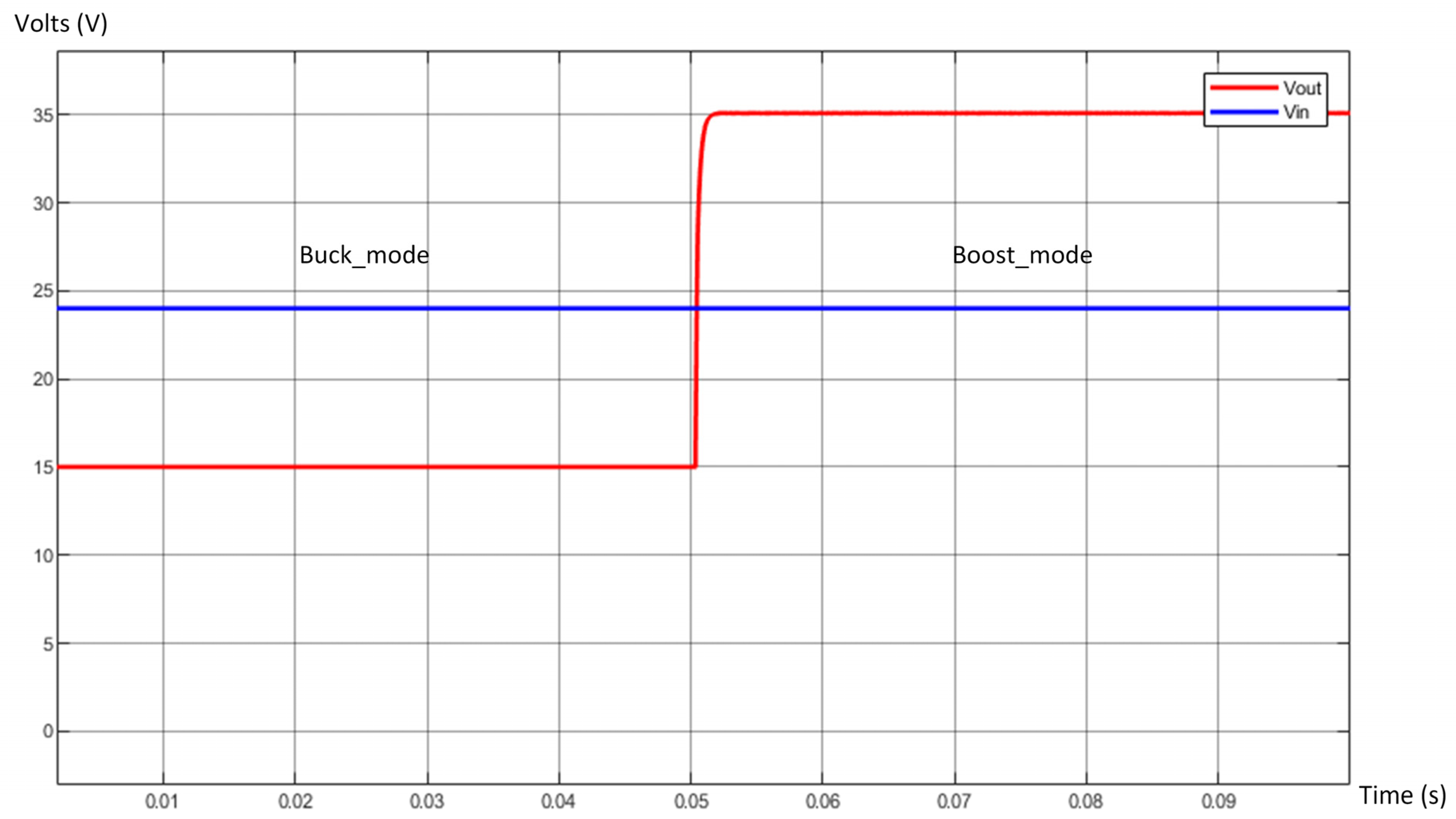
Figure 13 shows the output response of mode switching when the input voltage was constant. When the mode changed, the output response remained fast and stable, tracking the reference voltage. The ATSMC-based converter could achieve smooth mode switching, as shown in Figure 12 and Figure 13.
Performance metrics such as the settling time (ST), load regulation rate, and linear regulation rate were used to evaluate the algorithm’s performance, and the corresponding performance parameters are shown in the table above. The settling time is the time it takes for the output voltage to reach the reference voltage from its initial state. We obtain it by measuring the time it takes for the output voltage to rise from zero volts to the reference voltage. The load regulation rate and linear regulation rate represent the degree of system stability, and the smaller their values, the more robust the system. Equation (40) is the formula for the load regulation rate with the following parameters: Vin = 24 V, Rmax = 40 Ω, Rmin = 10 Ω, and Rnum = 20 Ω, and Equation (41) is the formula for the linear regulation rate with the following parameters: R = 20 Ω, Vinmax = 30 V, Vinmin = 10 V, and Vinnum = 24 V.
Load   Regulation = V O ( R max ) V O ( R min ) V O ( R num ) ×   100 %
Line   Regulation = V O ( Vin max ) V O ( Vin min ) V O ( Vin num ) ×   100 %
The data for the traditional control methods PID and SMC were reproduced and tested based on references [19,21], respectively, while the data for fuzzy logic control (FLC) were calculated based on references [35,36]. Table 2 shows that the load regulation rates and linear regulation rates of the traditional control methods PID, FLC, and SMC were all around 1%. Specifically, the settling times (ST) of PID and FLC were approximately 20 ms, while for SMC, the ST was around 1 ms. Compared to the traditional control methods, the proposed ATSMC reduced the ST by at least 1 ms and decreased the load regulation rate and linear regulation rate by at least 1%. Therefore, the ATSMC proposed in this paper had the advantage of a faster response time and demonstrated superior performance in the load regulation and linear regulation.

5. Board Verification

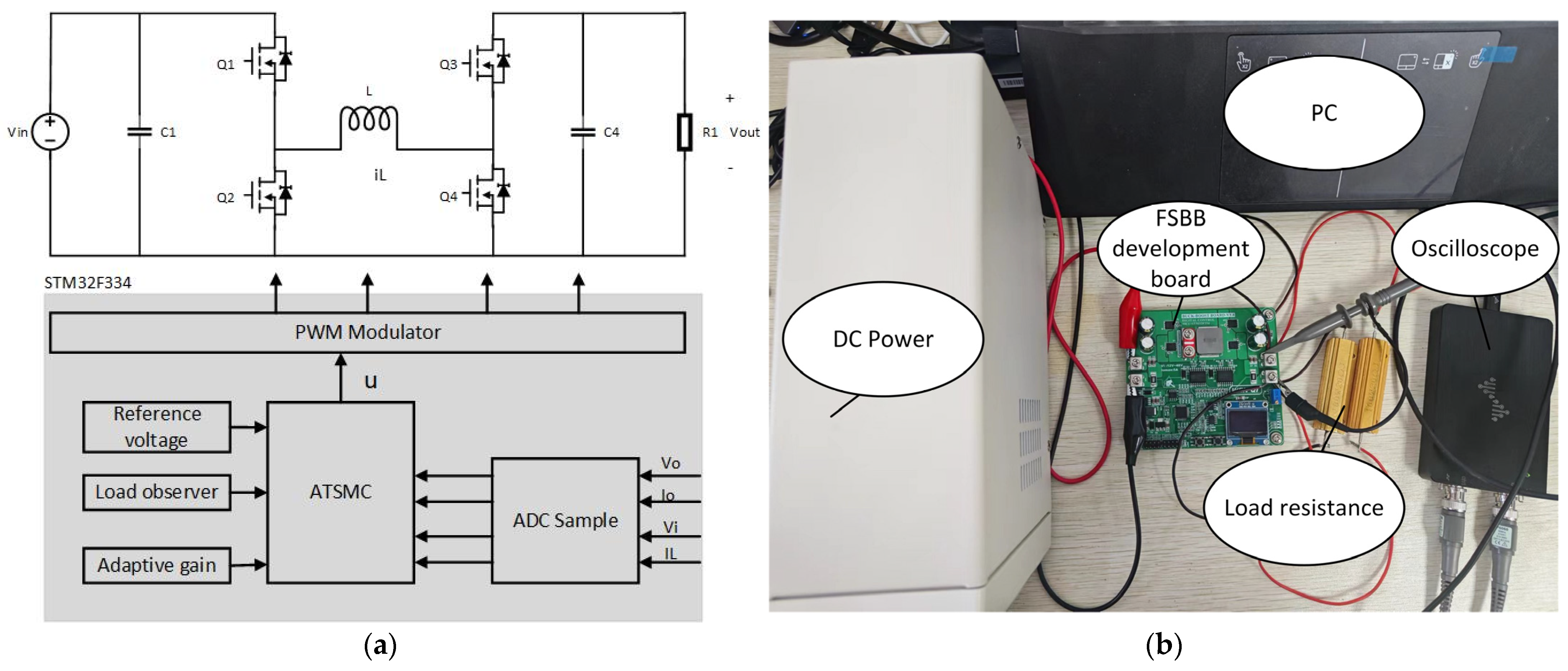
To further verify the superiority of the proposed control algorithm, an experimental platform was built in the laboratory, as shown in Figure 14. This platform consisted of an FSBB development board, a DC power supply, a reference voltage sliding relay, an auxiliary voltage, a sampling circuit, a load resistor, etc., and its parameters are shown in Table 3.
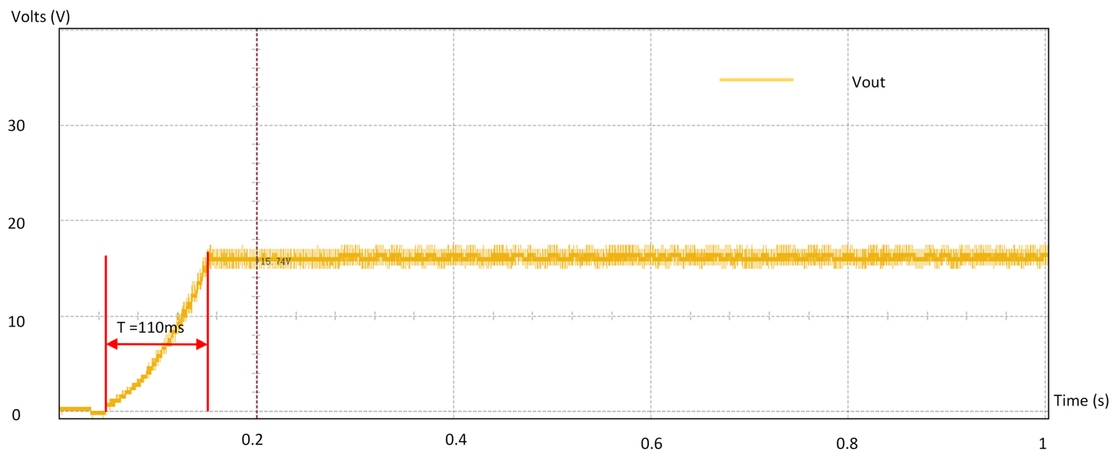
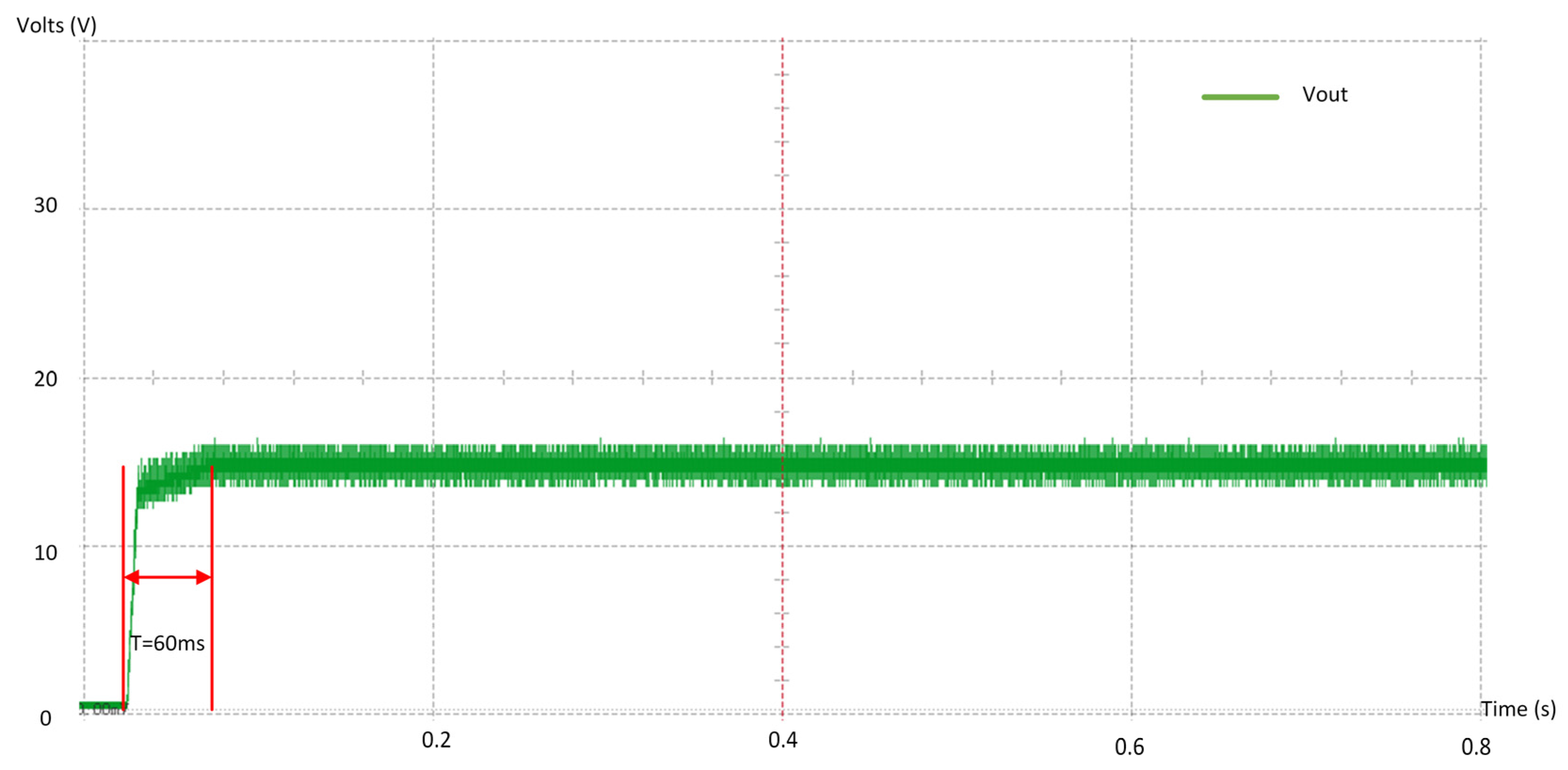
We compared the settling times (the times spent measuring the output voltage to reach the steady-state value of the reference voltage) of the conventional SMC and the ATSMC, and the results are shown in Figure 15 and Figure 16. The settling time of the traditional SMC was more than 100 ms, while the settling time of the ATSMC was around 60 ms, which was a much quicker response than that of the conventional SMC.
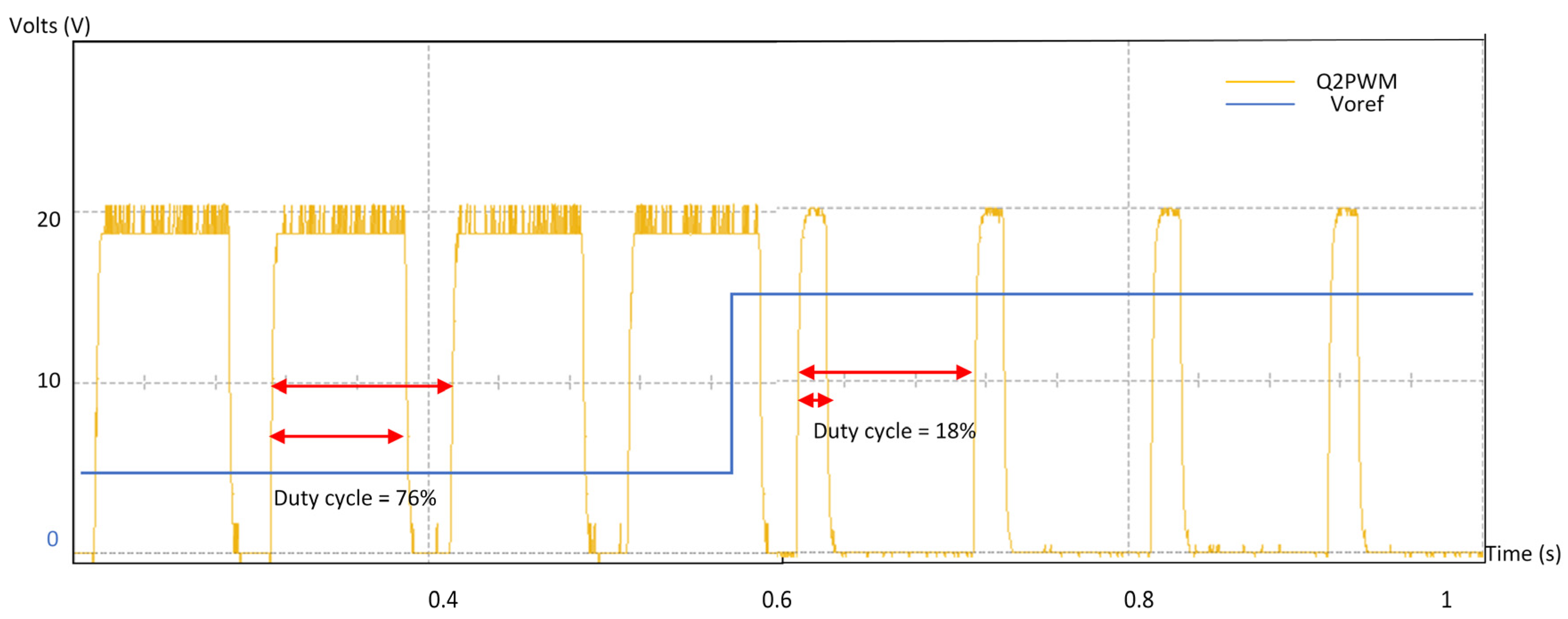
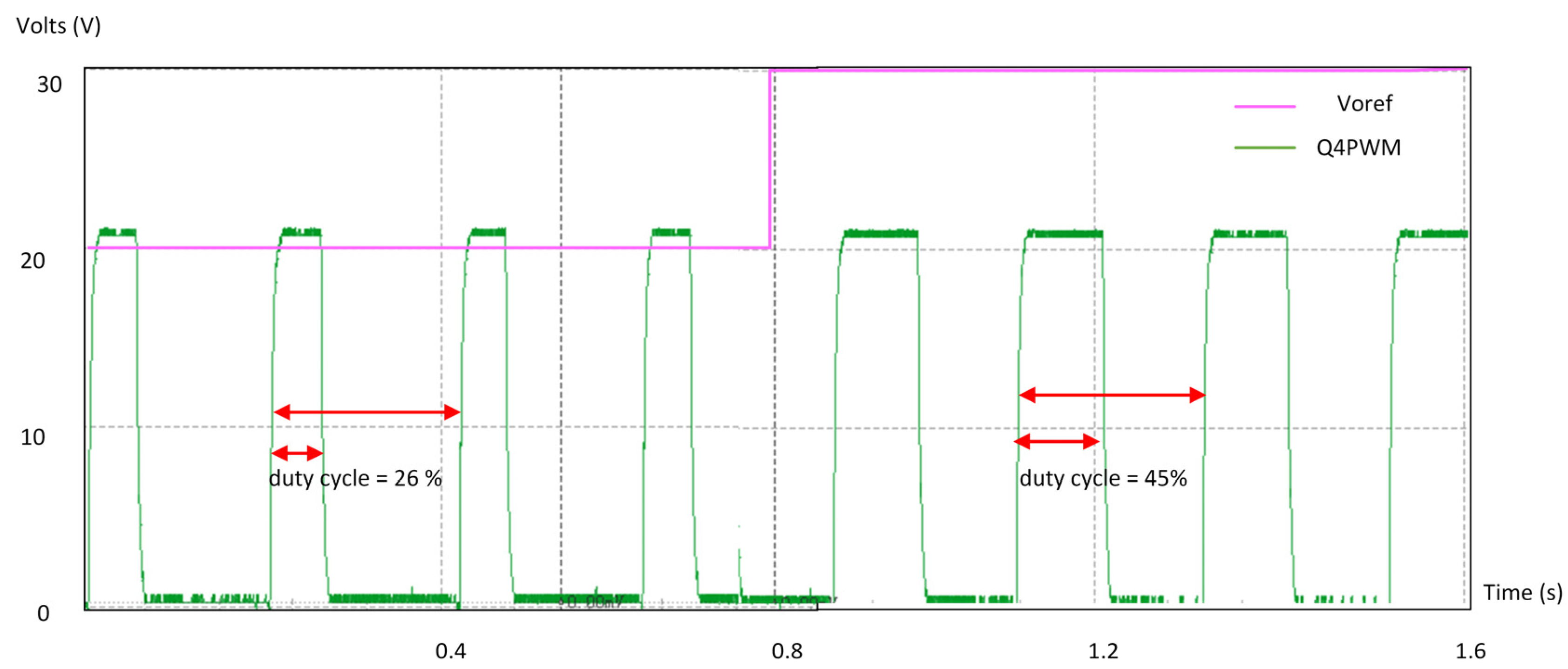
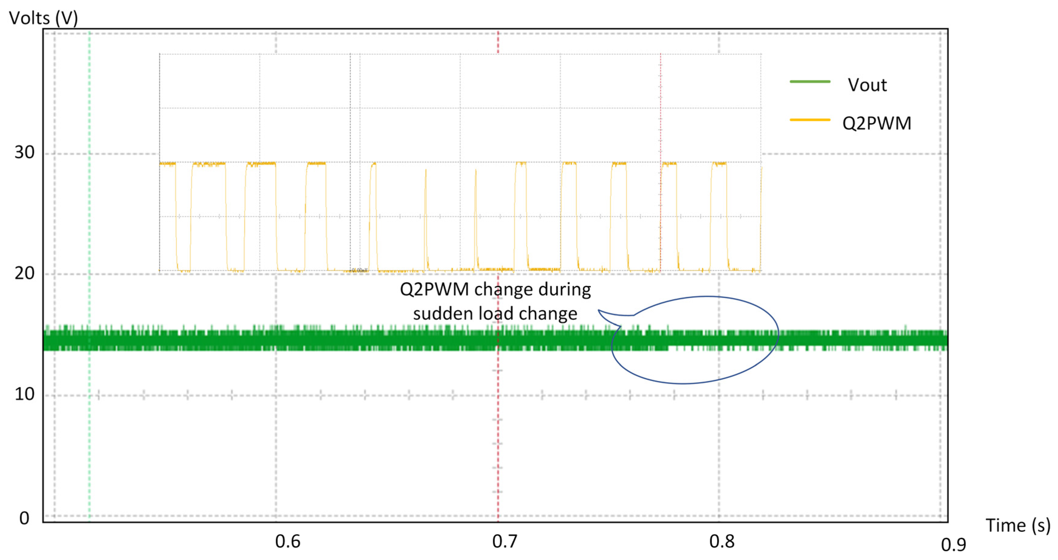
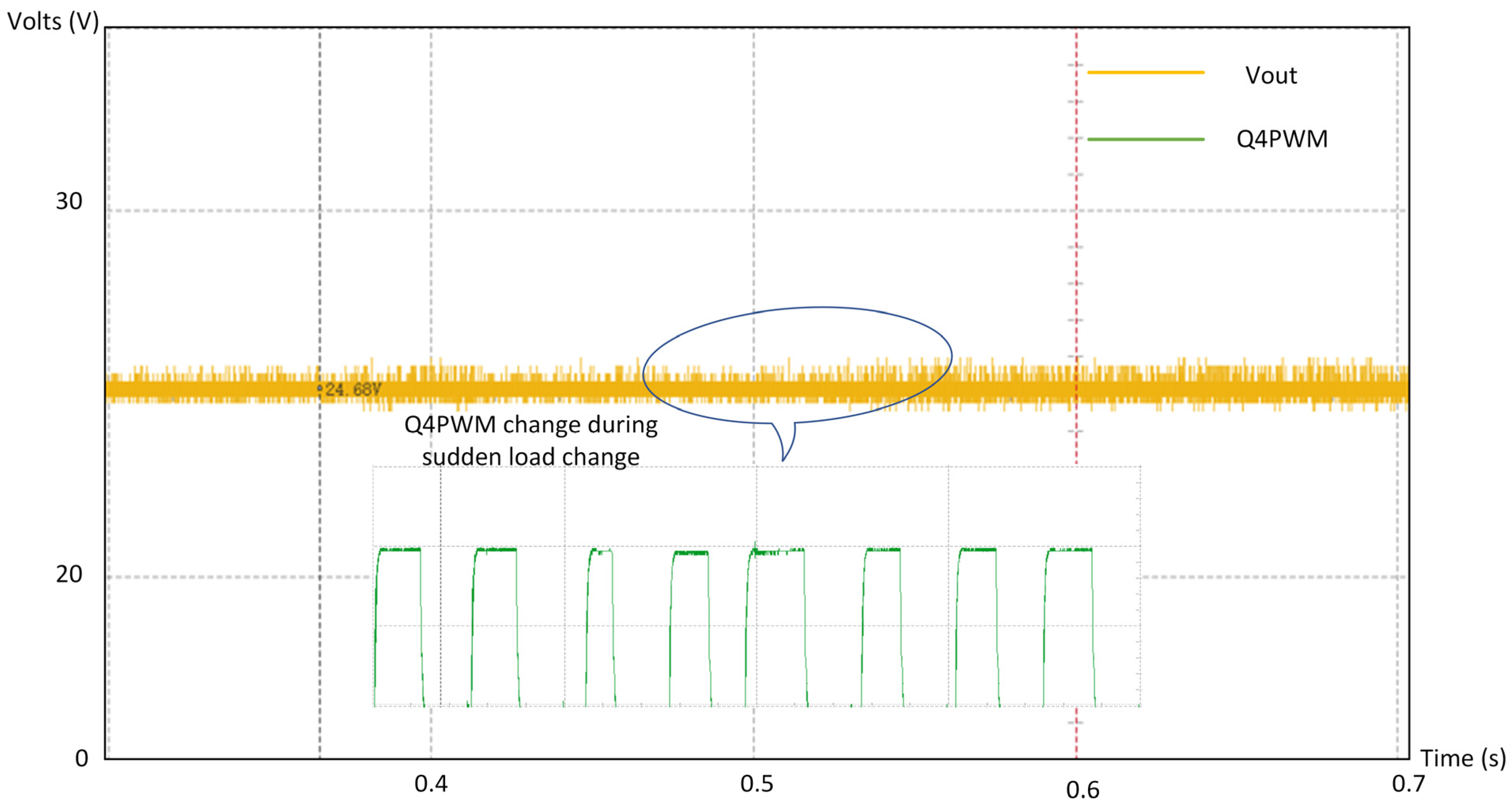
The experimental results of the FSBB switching tube duty cycles with step changes in the reference voltage are shown in Figure 17 and Figure 18. Since Q1 is the reverse of Q2 and Q3 is the reverse of Q4, when working in Buck mode, Q3 was usually disconnected, so only the duty cycle waveform of Q2 was intercepted, as shown in Figure 17. Considering the period with a dead-time setup, it can be seen in Figure 17 that with a change in the reference voltage, the duty cycle could respond quickly. When working in Boost mode, Q1 was usually disconnected, and the duty cycle waveform of Q4 was intercepted. The experimental results are shown in Figure 18, and the combination of Figure 17 and Figure 18 shows that the proposed algorithm had a good response speed.
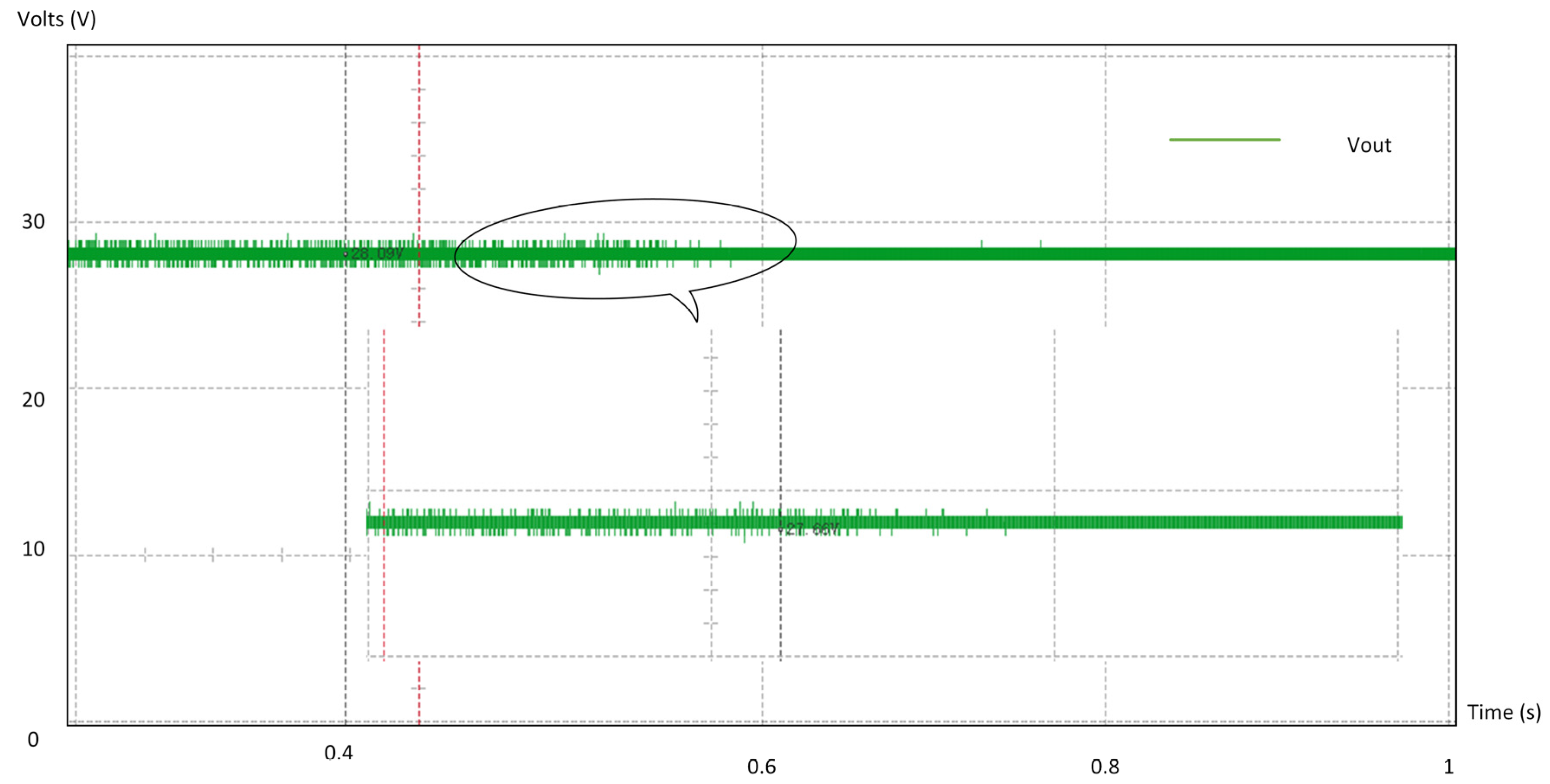
In Buck mode, the input voltage underwent a step change from 20 V to 25 V, and the output voltage is shown in Figure 19. It can be seen that the proposed algorithm had excellent linear regulation. The load resistance underwent a step change from 20 Ω to 10 Ω, and Figure 20 shows the output voltage versus the duty cycle. It can be seen that the fast-response duty cycle ensured that the converter had good load regulation capability. Based on Figure 19 and Figure 20, the proposed method had excellent transient performance in Buck mode.
In Boost converter mode, when the load resistance changed abruptly from 20 Ω to 10 Ω, the output voltage and duty cycle, as illustrated in Figure 21, demonstrated that the duty cycle could be quickly and stably adjusted, allowing the output voltage to consistently follow the reference voltage. The input voltage was shifted from 20 V to 25 V, and the resulting output voltage, which remained predominantly stable, is depicted in Figure 22. Based on the observations in Figure 21 and Figure 22, it can be concluded that the proposed method displayed excellent transient performance in Boost mode.
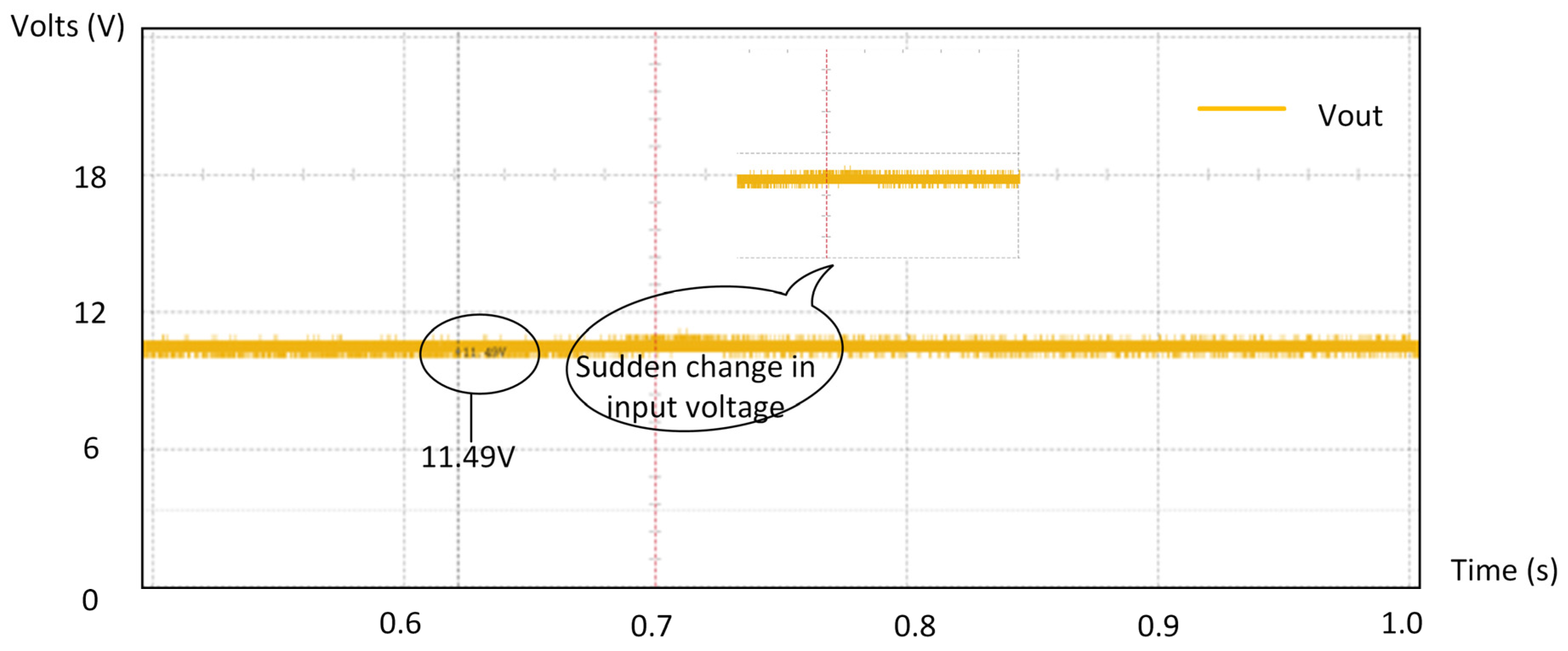
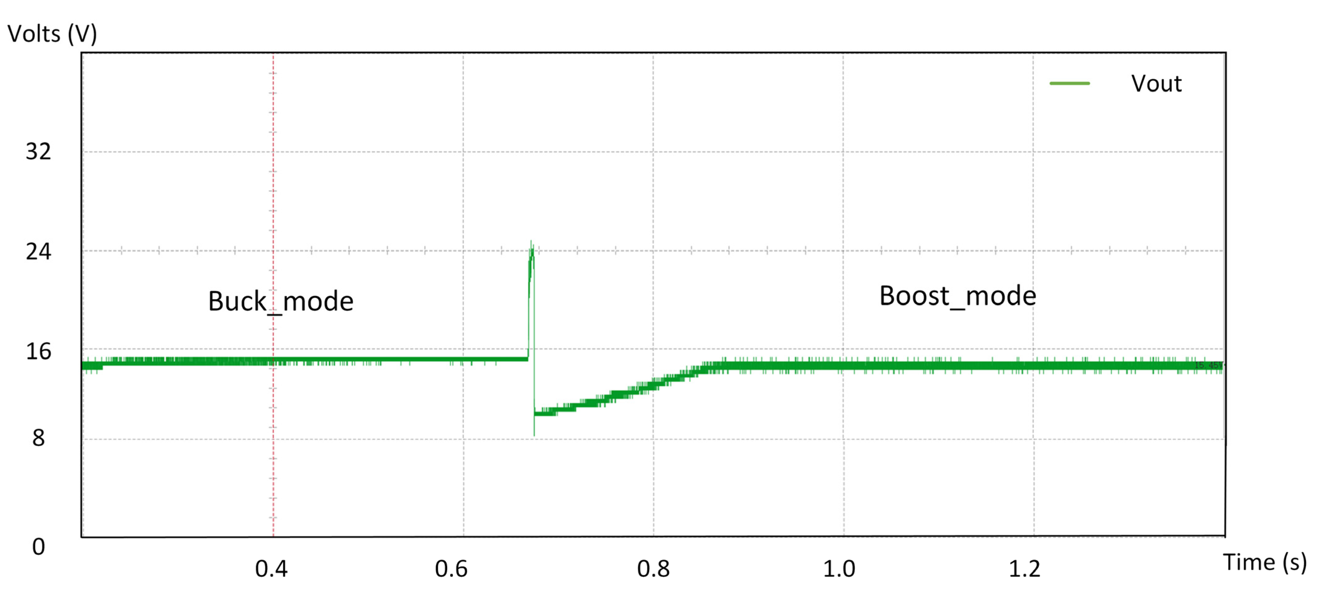
While the output voltage was constant at 15 V, the input voltage was changed from 22 V to 12 V to verify the proposed method, and the output response is shown in Figure 23. It can be seen that when mode switching occurred in the converter, the output voltage remained smooth and stable. This also verified that the proposed control method was able to achieve smooth switching in FSBB mode.
Table 4 compares the performance parameters of various algorithms in the hardware-in-the-loop test. It shows that the ATSMC algorithm reduced the settling times by 127 ms and 286 ms in Buck and Boost modes, respectively, compared to the conventional PID. In addition, the ATSMC also reduced the settling time by about 60 ms compared to the traditional SMC. The ATSMC reduced the load regulation and linear regulation rates by about 10% and 5%, respectively, compared to the conventional PID and by about 2% compared to the SMC. Therefore, the proposed ATSMC had superior transient and steady-state performances compared to the traditional control methods.

6. Conclusions

To improve the interference immunity and response speed of the FSBB converter, the main contribution of this work was to design a new global fast integral terminal sliding mode control method for controlling the FSBB converter, which can effectively improve the transient performance and robustness of the system compared with the traditional control method. It can effectively allow the system to converge in a finite time. Combined with the adaptive algorithm and real-time updating of the algorithm’s parameters, it can suppress jitter without affecting the response speed, which can effectively improve the flexibility and robustness of the system under different operating conditions.
The effectiveness of the proposed controller was confirmed via simulation and an experimental setup. By simulating the conventional control algorithms with ATSMC under different operating conditions, the steady-state performance of the output voltage and the system’s output responses in the face of disturbances were tested, which are common application cases of DC-DC converters. The experimental results show that ATSMC has a better anti-interference ability and better transient characteristics than FLC, PID, SMC, and TSMC, but due to the complexity of its algorithmic structure, the execution time of a single operation is too long. The next step is to perform hardware acceleration for the algorithm to reduce the cycle time of a single operation and, at the same time, to apply the algorithm to other DC-DC converters.

Author Contributions

Conceptualization, B.M. and J.J.; methodology, B.M.; software, B.M.; validation, B.M., J.J. and Z.Y.; formal analysis, B.M.; investigation, B.M. and J.J.; resources, J.J.; data curation, Z.Y.; writing—original draft preparation, B.M.; writing—review and editing, J.J. and Z.Y.; visualization, B.M.; supervision, J.J.; project administration, J.J. funding acquisition, B.M. All authors have read and agreed to the published version of the manuscript.

Funding

This research received no external funding.

Data Availability Statement

All data is contained within the article.

Conflicts of Interest

The authors declare no conflict of interest.

References

  1. Xu, Q.; Zhang, C.; Wen, C.; Wang, P. A novel composite nonlinear controller for stabilization of constant power load in DC microgrid. IEEE Trans. Smart Grid 2017, 10, 752–761. [Google Scholar] [CrossRef]
  2. Janabi, A.; Wang, B. Switched-capacitor voltage boost converter for electric and hybrid electric vehicle drives. IEEE Trans. Power Electron. 2019, 35, 5615–5624. [Google Scholar] [CrossRef]
  3. Pinto, R.A.; Cosetin, M.R.; Bolzan, T.E.; Marchesan, T.B.; Campos, A.; Alonso, J.M.; Prado, R.N. A bidirectional buck-boost converter to supply LEDs from batteries during peak load time. In Proceedings of the IECON 2011—37th Annual Conference of the IEEE Industrial, Melbourne, VIC, Australia, 7–10 November 2011. [Google Scholar]
  4. Linares, J.; Barahona, J.L.; Sira, H.; Contreras, M.A. Robust passivity-based control of a buck–boost-converter/DC-motor system: An active disturbance rejection approach. IEEE Trans. Ind. Appl. 2012, 48, 2362–2371. [Google Scholar] [CrossRef]
  5. Chen, I.C.; Liang, C.W.; Tsai, T.H. A single-inductor dual-input dual-output DC–DC converter for photovoltaic and piezoelectric energy harvesting systems. IEEE Trans. Circuits Syst. II Express Briefs 2019, 66, 1763–1767. [Google Scholar] [CrossRef]
  6. Camara, M.B.; Gualous, H.; Gustin, F.; Berthon, A.; Dakyo, B. DC/DC converter design for supercapacitor and battery power management in hybrid vehicle applications—Polynomial control strategy. IEEE Trans. Ind. Electron. 2009, 57, 587–597. [Google Scholar] [CrossRef]
  7. Khan, M.A.; Ahmed, A.; Husain, I.; Sozer, Y.; Badawy, M. Performance analysis of bidirectional DC–DC converters for electric vehicles. IEEE Trans. Ind. Appl. 2015, 51, 3442–3452. [Google Scholar] [CrossRef]
  8. Yong, J.; Xu, X.; Zeng, L.; Li, L. A review of low voltage DC power distribution system. Proc. CSEE 2013, 33, 42–52. [Google Scholar]
  9. Zhang, N.; Zhang, G.; See, K.W. Systematic derivation of dead-zone elimination strategies for the noninverting synchronous buck–boost converter. IEEE Trans. Power Electron. 2017, 33, 3497–3508. [Google Scholar] [CrossRef]
  10. Orellana, M.; Petibon, S.; Estibals, B.; Alonso, C. Four switch buck-boost converter for photovoltaic DC-DC power applications. In Proceedings of the IECON 2010—36th Annual Conference on IEEE Industrial Electronics Society, Glendale, AZ, USA, 7–13 November 2010. [Google Scholar]
  11. Lee, H.S.; Yun, J.J. High-efficiency bidirectional buck–boost converter for photovoltaic and energy storage systems in a smart grid. IEEE Trans. Power Electron. 2018, 34, 4316–4328. [Google Scholar] [CrossRef]
  12. Waffler, S.; Kolar, J.W. A novel low-loss modulation strategy for high-power bidirectional buck + boost converters. IEEE Trans. Power Electron. 2009, 24, 1589–1599. [Google Scholar] [CrossRef]
  13. Huang, P.C.; Wu, W.Q.; Ho, H.H.; Chen, K.H. Hybrid buck–boost feedforward and reduced average inductor current techniques in fast line transient and high-efficiency buck–boost converter. IEEE Trans. Power Electron. 2009, 25, 719–730. [Google Scholar] [CrossRef]
  14. Ren, X.; Ruan, X.; Qian, H.; Li, M.; Chen, Q. Three-mode dual-frequency two-edge modulation scheme for four-switch buck–boost converter. IEEE Trans. Power Electron. 2008, 24, 499–509. [Google Scholar]
  15. Chen, C.W.; Chen, K.H.; Chen, Y.M. Modeling and controller design of an autonomous PV module for DMPPT PV systems. IEEE Trans. Power Electron. 2013, 29, 4723–4732. [Google Scholar] [CrossRef]
  16. Kim, S.K.; Lee, K.B. Robust feedback-linearizing output voltage regulator for DC/DC boost converter. IEEE Trans. Ind. Electron. 2015, 62, 7127–7135. [Google Scholar] [CrossRef]
  17. Sarvi, M.; Soltani, I.; NamazyPour, N.; Rabbani, N. A New Sliding Mode Controller for DC/DC Converters in Photovoltaic Systems. J. Energy 2013, 2013, 871025. [Google Scholar] [CrossRef]
  18. Mohammadzamani, F.; Hashemi, M.; Shahgholian, G. Adaptive neural control of non-linear fractional order multi-agent systems in the presence of error constraints and input saturation. IET Control Theory Appl. 2022, 16, 1283–1298. [Google Scholar] [CrossRef]
  19. Cai, J.; Zhao, Y.; Hou, Y.; Chen, Y. Research on Control Strategy of Single-Mode Four-Switch Buck-Boost Converter. In Proceedings of the 2021 China Automation Congress (CAC), Beijing, China, 22–24 October 2021. [Google Scholar]
  20. Komurcugil, H.; Guler, N.; Bayhan, S. Lyapunov-function based control strategy for four-switch buck-boost dc-dc converters. In Proceedings of the 2022 IEEE 31st International Symposium on Industrial Electronics (ISIE), Anchorage, AK, USA, 1–3 June 2022. [Google Scholar]
  21. Ullah, Q.; Busarello, T.D.C.; Brandao, D.I.; Simões, M.G. Design and performance evaluation of SMC-based DC–DC converters for microgrid applications. Energies 2023, 16, 4212. [Google Scholar] [CrossRef]
  22. Tan, S.C.; Lai, Y.M.; Tse, C.K. A unified approach to the design of PWM-based sliding-mode voltage controllers for basic DC-DC converters in continuous conduction mode. IEEE Trans. Circuits Syst. I Regul. Pap. 2006, 53, 1816–1827. [Google Scholar]
  23. Ardhenta, L.; Rusli, M. Sliding mode control of output voltage in DC-DC Boost converter using PI sliding surface. In Proceedings of the 2021 International Conference on Electrical and Information Technology (IEIT), Malang, Indonesia, 14–15 September 2021. [Google Scholar]
  24. Qiao, L.; Zhang, W. Adaptive non-singular integral terminal sliding mode tracking control for autonomous underwater vehicles. IET Control Theory Appl. 2017, 11, 1293–1306. [Google Scholar] [CrossRef]
  25. Qiao, L.; Zhang, W. Adaptive second-order fast nonsingular terminal sliding mode tracking control for fully actuated autonomous underwater vehicles. IEEE J. Ocean. Eng. 2018, 44, 363–385. [Google Scholar] [CrossRef]
  26. Liu, P.; Wang, Z. Adaptive Discrete-Time Sliding Mode Control Design for Buck Converters with Disturbances. In Proceedings of the 2023 42nd Chinese Control Conference (CCC), Tianjin, China, 24–26 July 2023. [Google Scholar]
  27. Zambrano-Prada, D.; Aroudi, A.E.; Vázquez-Seiszdedos, L.; Lopez-Santos, O.; Haroun, R.; Martínez-Salamero, L. Adaptive Sliding Mode Control for a Boost Converter with Constant Power Load. In Proceedings of the 2023 IEEE Conference on Power Electronics and Renewable Energy (CPERE), Luxor, Egypt, 19–21 February 2023. [Google Scholar]
  28. Linares-Flores, J.; Heredia-Barba, R.; Heredia, O.; Castro-Heredia, G.; Curiel-Olivares, G.; Juarez-Abad, J.A. Adaptive sliding mode control based on a hyperbolic tangent function for DC-to-DC buck-boost power converter. In Proceedings of the 2020 IEEE Energy Conversion Congress and Exposition (ECCE), Detroit, MI, USA, 11–15 October 2022. [Google Scholar]
  29. Chang, Y.; Wang, A.; Gao, P.; Wang, Y.; Luo, M.; Huang, W. A non-singular terminal sliding mode control of the DC microgrid with constant power loads. In Proceedings of the 2023 IEEE 2nd Industrial Electronics Society Annual On-Line Conference (ONCON), Virtual, 8–10 December 2023. [Google Scholar]
  30. Chang, Y.; Gao, P.; Wang, A.; Wang, Y.; Zhang, C.; Huang, W. A Non-Singular Terminal Sliding Mode Control of Buck-Boost Converters Based on Extended State Observer. In Proceedings of the 2023 IEEE 2nd Industrial Electronics Society Annual On-Line Conference (ONCON), Virtual, 8–10 December 2023. [Google Scholar]
  31. Liu, Z.; Lin, X.; Gao, Y.; Xu, R.; Wang, J.; Wang, Y.; Liu, J. Fixed-time sliding mode control for DC/DC buck converters with mismatched uncertainties. IEEE Trans. Circuits Syst. I Regul. Pap. 2022, 70, 472–480. [Google Scholar] [CrossRef]
  32. Wang, Z.; Li, S.; Li, Q. Continuous nonsingular terminal sliding mode control of DC–DC boost converters subject to time-varying disturbances. IEEE Trans. Circuits Syst. II Express Briefs 2019, 67, 2552–2556. [Google Scholar] [CrossRef]
  33. Malge, S.V.; Ghogare, M.G.; Patil, S.L.; Deshpande, A.S.; Pandey, S.K. Chatter-free non-singular fast terminal sliding mode control of interleaved boost converter. IEEE Trans. Circuits Syst. II Express Briefs 2022, 70, 186–190. [Google Scholar] [CrossRef]
  34. Kaifei, Z.; Yiguang, C.; Haoran, Z.; Guowen, L. Fast Integral Terminal Sliding Mode Control of PMSM Based on New Sliding Mode Reaching Law. In Proceedings of the 2022 25th International Conference on Electrical Machines and Systems (ICEMS), Chiang Mai, Thailand, 29 November–2 December 2022. [Google Scholar]
  35. Sharma, K.; Palwalia, D.K. Robust controller design for DC-DC converters using fuzzy logic. In Proceedings of the 2017 4th International Conference on Signal Processing, Computing and Control (ISPCC), Solan, India, 21–23 September 2017. [Google Scholar]
  36. Guo, L.; Hung, J.Y.; Nelms, R.M. Evaluation of DSP-based PID and fuzzy controllers for DC–DC converters. IEEE Trans. Ind. Electron. 2009, 56, 2237–2248. [Google Scholar]
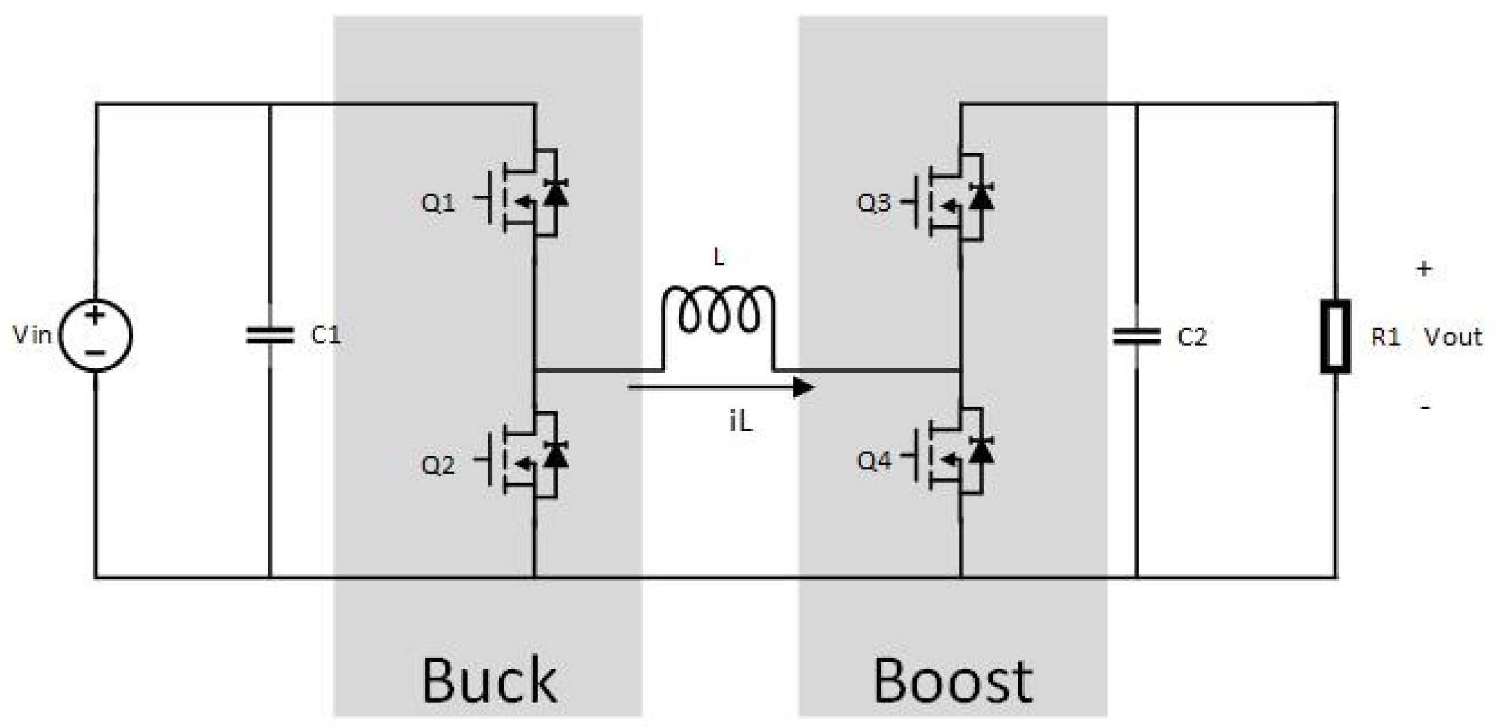
Figure 1. FSBB topology.
Energies 17 03645 g001
Figure 2. Buck working mode. (a) Interval (d1)T; (b) Interval (1 – d1)T.
Energies 17 03645 g002
Figure 3. Boost working mode. (a) Interval (d2)T; (b) Interval (1 – d2)T.
Energies 17 03645 g003
Figure 4. Block diagram of ATSMC Boost mode (1, 2, 3, 4 are Vo, Iin, Vin, Iout respectively).
Energies 17 03645 g004
Figure 5. Block diagram of ATSMC Buck mode (1, 2, 3, 4 are Vo, Iin, Vin, Iout respectively).
Energies 17 03645 g005
Figure 6. Output voltage tracking effect in Buck mode.
Energies 17 03645 g006
Figure 7. Output voltage tracking effect in Boost mode.
Energies 17 03645 g007
Figure 8. Voltage responses when load changed in Buck mode.
Energies 17 03645 g008
Figure 9. Voltage responses when load changed in Boost mode.
Energies 17 03645 g009
Figure 10. Output voltage responses when input changed in Buck mode.
Energies 17 03645 g010
Figure 11. Output voltage responses when input changed in Boost mode.
Energies 17 03645 g011
Figure 12. Mode switching based on ATSMC converter (changing input voltage).
Energies 17 03645 g012
Figure 13. Mode switching based on ATSMC converter (changing output voltage).
Energies 17 03645 g013
Figure 14. The experimental device: (a) a block diagram of the experimental device; (b) a photo of the experimental device.
Energies 17 03645 g014
Figure 15. Output response of SMC algorithm in Buck mode.
Energies 17 03645 g015
Figure 16. Output response of ATSMC algorithm in Buck mode.
Energies 17 03645 g016
Figure 17. Duty cycle change during step change in ATSMC reference voltage in Buck mode.
Energies 17 03645 g017
Figure 18. Duty cycle change during step change in ATSMC reference voltage in Boost mode.
Energies 17 03645 g018
Figure 19. ATSMC input voltage surges in Buck mode.
Energies 17 03645 g019
Figure 20. Sudden changes in ATSMC load resistance in Buck mode.
Energies 17 03645 g020
Figure 21. Sudden change in ATSMC load resistance in Boost mode.
Energies 17 03645 g021
Figure 22. ATSMC input voltage surges in Boost mode.
Energies 17 03645 g022
Figure 23. FSBB mode switching effect.
Energies 17 03645 g023
Table 1. Performance analysis. Controller performance indicators.
ReferencesPublication YearControl MethodsControl ModelChallenges
Cai, J. [19]2021PID-2p2zFSBBMore extended system settling times.
Ullah, Q. [21]2023Sliding mode controlFSBBThe systematic error can no longer converge in a finite time.
Liu, P. [26]2023Adaptive sliding
mode control
BuckCombining observers improves tracking accuracy but increases design complexity.
Zambrano-Prada, D. [27]2023Adaptive sliding
mode control
BoostThe hyperbolic tracking error slows down the system’s responses.
Liu, Z. [31]2023Terminal sliding
mode control
BuckA second-order, fixed-time convergence law improves the algorithm complexity.
Wang, Z. [32]2020Terminal sliding
mode control
BoostA finite-time perturbation observer increases the complexity of the design structure.
Kaifei, Z. [34]2022Terminal sliding
mode control
permanent magnet synchronous motorFast integral terminal sliding mode control effectively improves the dynamic characteristics of the system but cannot cope with variable operating environments.
Table 2. Controller performance indicators.
Test AlgorithmModeST (ms)Load RegulationLine Regulation
FLC [35]
PID [19]
SMC [21]
TSMC
Buck101.84%0.96%
212.3%1.04%
1.31
0.4
1.67%
0.33%
0.77%
0.083%
ATSMC0.510.25%0.027%
FLC [36]
PID [19]
SMC [21]
Boost172.3%1.1%
19
5
1.6%
0.9%
1.2%
0.6%
TSMC
ATSMC
2.50.16%0.083%
20.03%0.03%
Table 3. Experimental device circuit parameters.
DescriptionSymbolNominal Value
Output VoltageVo5–48 V
Input VoltageVin10–30 V
InductanceL22 uH
CapacitanceC440 uF
Minimum Load ResistanceR(min)10 Ω
Maximum Load ResistanceR(max)30 Ω
Switch FrequencyFs200 kHz
Table 4. Board machine verification performance comparison.
Test AlgorithmModeST (ms)Load RegulationLine Regulation
PID 18814.5%8.2%
SMCBuck1412.2%1.9%
ATSMC 600.8%0.33%
PID
SMC
ATSMC
Boost401
178
9.4%
1.54%
6.3
1.33%
1100.16%0.15%
Disclaimer/Publisher’s Note: The statements, opinions and data contained in all publications are solely those of the individual author(s) and contributor(s) and not of MDPI and/or the editor(s). MDPI and/or the editor(s) disclaim responsibility for any injury to people or property resulting from any ideas, methods, instructions or products referred to in the content.