Abstract
This study presents a novel soft-switching inverter distinguished by a simplified topology and an innovative modulation approach. The design aims to optimize the energy conversion processes commonly found in auxiliary snubber circuits. By minimizing the number of auxiliary switches, the control method is streamlined, thereby enhancing system reliability and cost-efficiency. The principles of operation and conditions for soft-switching are thoroughly analyzed using equivalent circuit models. A 3 kW/16 kHz inverter prototype was constructed, and the experimental results confirm the effectiveness and benefits of the proposed inverter.
1. Introduction
Soft-switching technology, when integrated with ASCs in hard-switching inverters, offers a notable advantage. The ability of soft-switching inverters to operate in environments with either zero-voltage or zero-current conditions effectively reduces switching losses. This reduction is pivotal for accommodating higher switching frequencies, enhancing the overall performance and efficiency of inverter systems. Moreover, the incorporation of soft-switching techniques leads to a substantial reduction in dv/dt and di/dt across the switches. This mitigation is essential for diminishing electromagnetic interference, a common issue that can compromise the reliability and efficiency of power electronic devices [1,2].
Among various soft-switching inverters, the auxiliary resonant inverter stands out. It includes resonant DC-link inverters [3,4,5,6,7] and auxiliary resonant commutated pole (ARCP) inverters [8,9,10,11,12,13,14,15,16,17,18,19,20,21,22,23,24], depending on the position of the ASC in the inverter. The ASC of the ARCP inverter is active only for a short duration during the switching cycle, which greatly reduces the losses generated by the ASC. Due to these advantages, ARCP inverters have attracted considerable interest from researchers and professionals in the field.
The ARCP inverter introduced in [9,10] is renowned for its ability to achieve comprehensive soft-switching. After that, there are various ARCP inverter variants, including delta or star inverters [11,12], coupled inductor inverters [13,14,15,16], and transformer-assisted inverters [17,18,19], among others. Despite their advancements, these inverters face significant challenges. For instance, the use of large electrolytic capacitors can lead to inherent issues, such as neutral point voltage variation, which can affect the stability and performance of the inverter. Furthermore, in practical implementations, three-phase ASCs are often interconnected, which not only complicates the control strategies but also increases the overall physical size and complexity of the system. These complications can hinder the efficiency and feasibility of deploying such inverters in real-world applications, highlighting the need for more streamlined and effective design solutions.
In [21], a novel ARCP inverter was introduced to overcome the limitations of previous soft-switching inverter designs. This innovative approach effectively reduced switching losses and enhanced overall efficiency by implementing indirect soft-switching for the auxiliary switches. This design successfully resolved several critical issues found in earlier topologies, such as high switching stress and energy inefficiencies. However, despite these advancements, the new inverter still encounters significant challenges in high-power applications. Specifically, parasitic parameters negatively impact the ZVS turn-off process, causing inefficiencies and raising potential reliability concerns. These parasitic effects can degrade performance under high-power conditions, underscoring the necessity for further refinement and optimization to fully realize the soft-switching inverter’s potential.
To address the above challenges, a series of double ARCP inverters have been proposed [22,23,24]. In [22], a reliable zero-voltage switching (ZVS) turn-off condition is achieved by directly connecting capacitors in parallel with the auxiliary switches. Despite this improvement, the inverter still experiences high losses and significant current stress on the auxiliary switches. Building on this work, [23] introduces an additional set of auxiliary switches and proposes an optimized modulation strategy, effectively reducing the current stress on these switches. However, the complexity and coupling of the commutation resonance process in this topology lead to system oscillations. To address these issues, [24] presents an auxiliary circuit using only two resonant inductors, which helps decouple the resonant process and enhances system reliability. Nonetheless, the use of multiple auxiliary switches in [23,24] results in high hardware costs, complicated control schemes, and reduced reliability.
Recognizing the limitations of the abovementioned double ARCP inverters, this paper proposes a novel ARCP inverter design that aims to resolve these issues. The key features and benefits of the proposed inverter include the following:
- (1)
- All switches can reliably achieve soft-switching, reducing switching losses and improving efficiency;
- (2)
- The ASC is designed with a simple structure, requiring fewer components, which simplifies the overall system design;
- (3)
- The proposed inverter operates with fewer modes and achieves higher transmission efficiency, further enhancing performance and reducing complexity.
2. Circuit Topology and Operation Principle
2.1. Circuit Topology
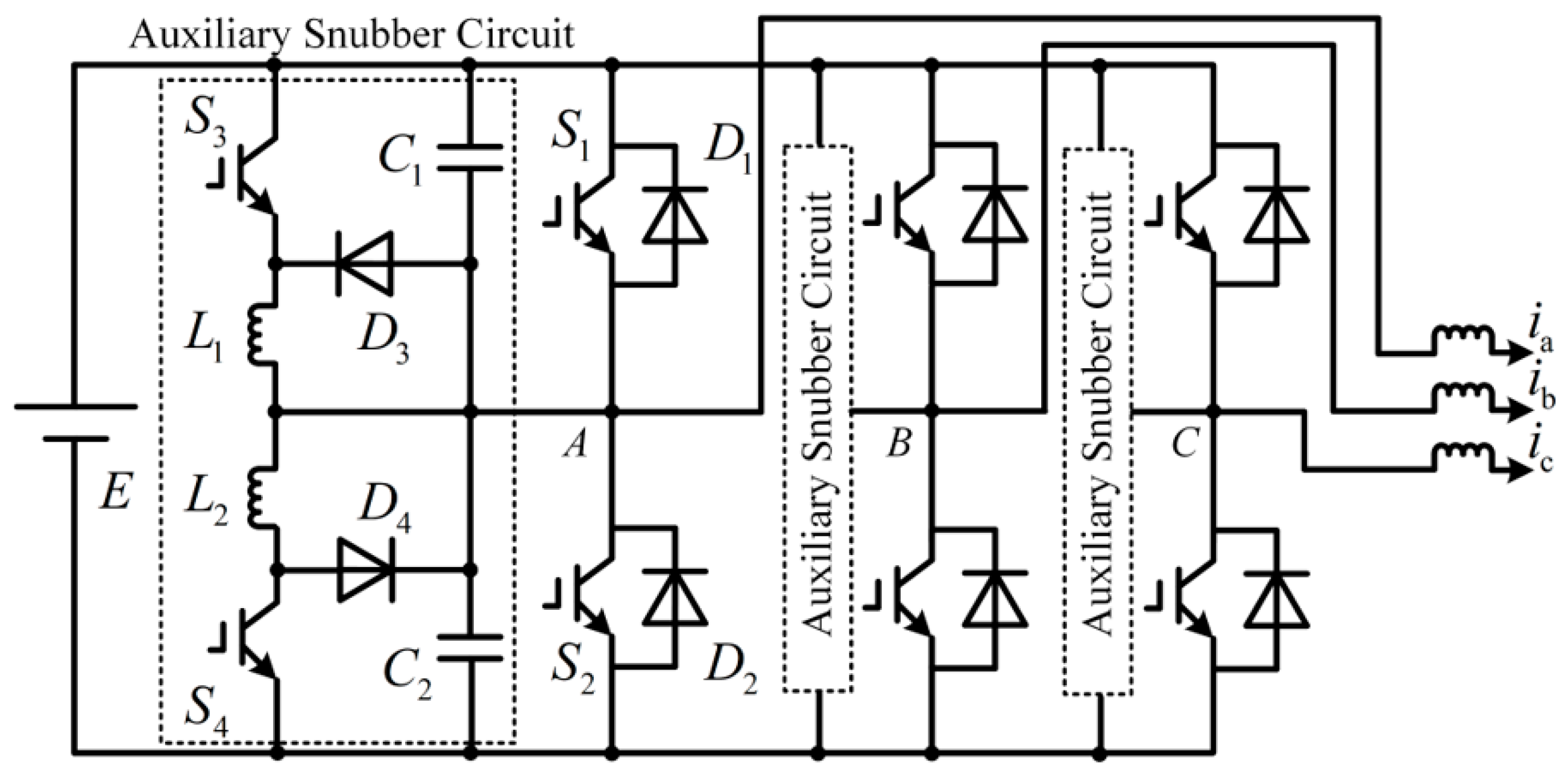
The layout of the proposed soft-switching inverter is illustrated in Figure 1. As shown, the structure and commutation principles are uniform across all phases, allowing phase A to serve as a representative example for analysis [21]. Given the short switching period, it is reasonable to assume that the current remains constant during this interval.

Figure 1.
The three-phase ARCP inverter with simple topology.
Figure 2 presents the equivalent circuit for phase A. The dashed section highlights the ASC, which is designed to optimize the switching conditions of switches (S1, S2). The ASC includes resonant capacitors (C1, C2), resonant inductors (L1, L2), auxiliary switches (S3, S4), and auxiliary diodes (D3, D4). C1(C2) is connected in parallel with S1 and S3 (S2 and S4), which limits the voltage change rate and switches can achieve ZVS turn-off. L1 (L2) is connected in series with S3 (S4), which limits the rate of change of the current through S3(S4), thereby minimizing turn-on losses and ensuring ZCS turn-on for S3 (S4).
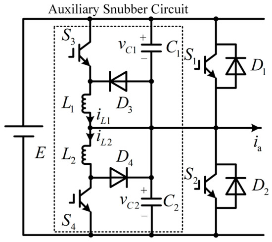
Figure 2.
Equivalent circuit for phase A.
2.2. Operation Principle
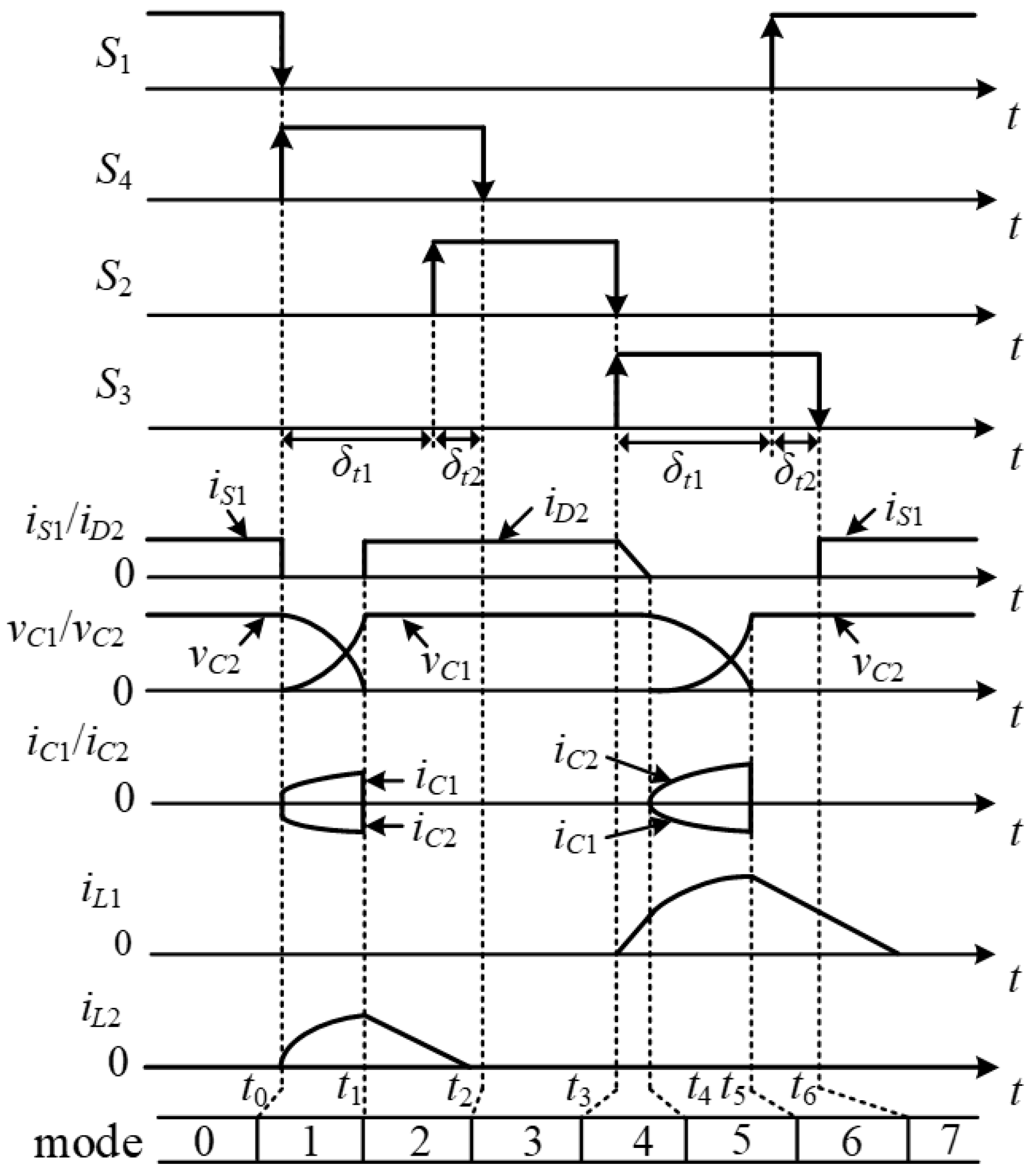
The modulation strategy and theoretical waveforms are depicted in Figure 3. The action sequence of switches is as follows: initially, S1 (S2) is turned OFF, followed immediately by the activation of S4 (S3). After a delay period δt1, S2 (S1) is then turned on. Subsequently, after another delay δt2, S4 (S3) is turned off. This sequence ensures effective soft-switching with minimal losses. (S1, S2) are modulated according to the sinusoidal pulse width modulation (SPWM), and they operate under the complementary conduction mode with a 180-degree phase difference.
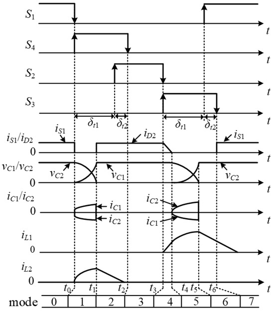
Figure 3.
Theoretical waveforms for main component operations.
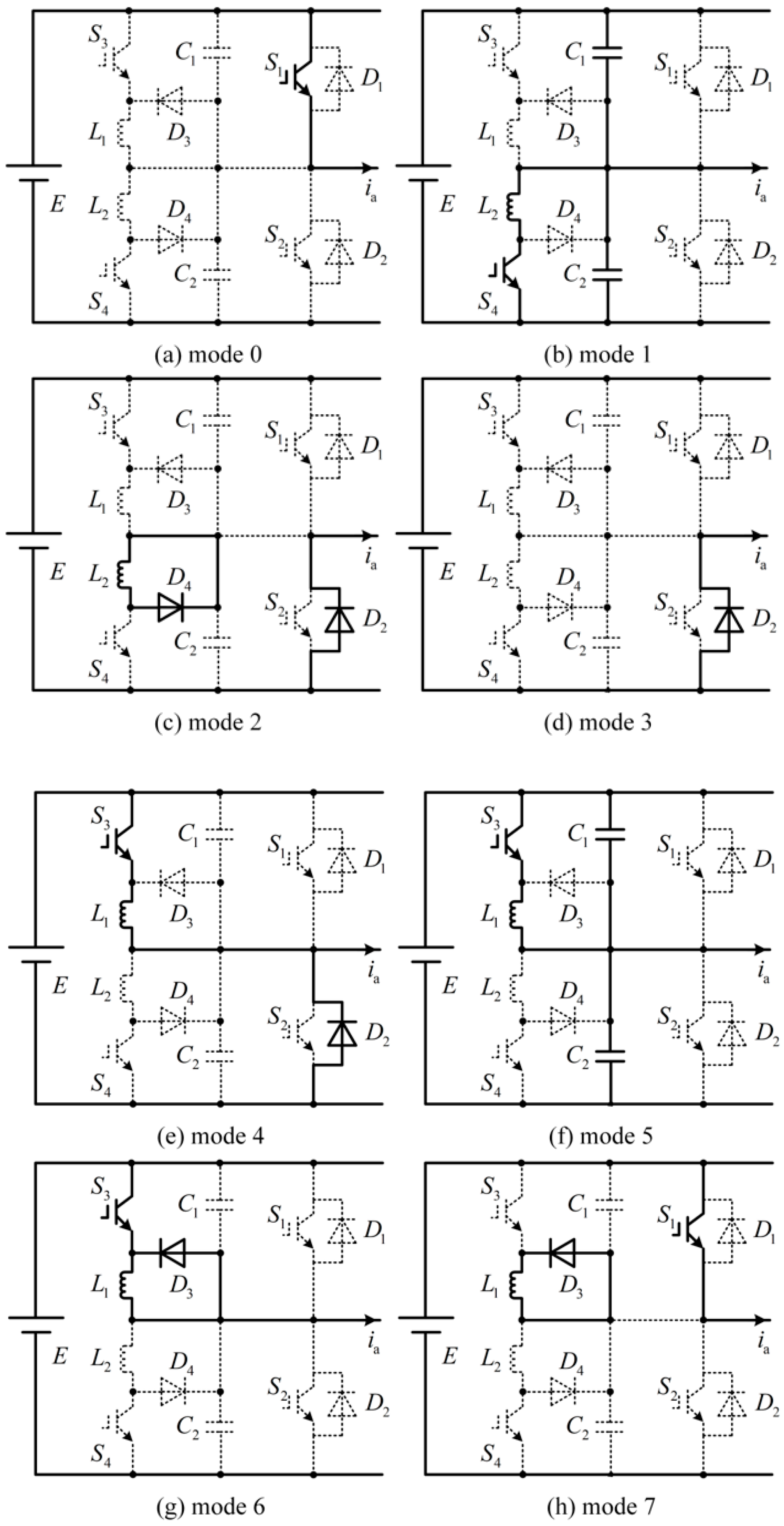
The auxiliary resonant capacitances and auxiliary resonant inductances are designed as C1 = C2 = C and L1 = L2 = L. Due to the short duration of the commutation time, ia remains approximately constant. The commutation process of the inverter is structured into eight distinct modes, with each mode’s equivalent circuit illustrated in Figure 4.
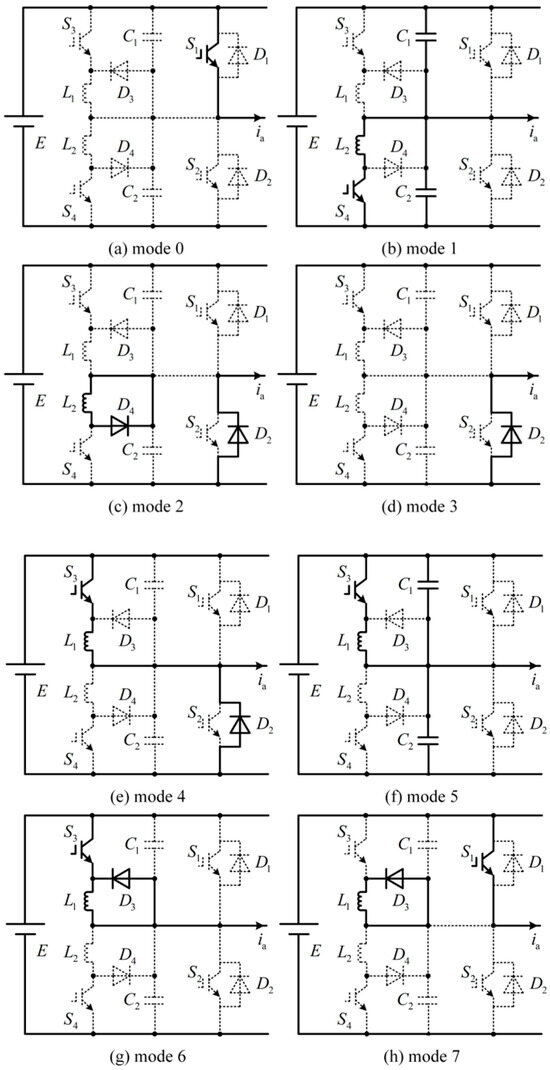
Figure 4.
Equivalent circuits for various operation modes.
Mode 0 [~t0]: Before t0, S1 is conducting, while S2, S3 and S4 are non-conducting. At this stage, ia flows through S1. The initial conditions of the resonant elements are specified as vC1(t0) = 0, vC2(t0) = E, iL1(t0) = iL2(t0) = 0.
Mode 1 [t0~t1]: At t0, S1 is switched off, and S4 is immediately turned on. This initiates resonance in C1, C2, and L2, causing the currents through L2 to rise. The voltage across C1 begins increasing from zero, while the voltage across C2 starts decreasing from E. Under the effect of L2, S4 achieves a pseudo-ZCS turn-on. When S1 is turned off, vC1 rises resonantly from zero, so S1 achieves a pseudo-ZVS turn-off. vC1, vC2, iL1, and iL2 are as follows:
where: .
When vC1 rises to E, vC2 drops to zero and iL2 reaches the maximum value, iL2max. At this point, D2 and D4 start conducting, signaling the end of mode 1. The duration t0–1 of mode 1 is given by the following:
Mode 2 [t1~t2]: At t1, vC1 rises to E, vC2 drops to zero, and D2 and D4 start conducting. Because the sum of the forward voltages of S4 and D2 is greater than the forward voltage of D4, iL2 flows through D4, rather than D2. ia is carried by D2, and iL2 flows through D4. vL2 equals the forward voltage of D4, and iL2 starts to decrease from iL2max linearly. When iL2 decreases to zero, the process concludes, which is independent of other modes. S2 is turned on during D2 conduction, and S2 realizes the ZVZCS turn-on. Mode 2 ends when S4 is turned off.
The discharge time of L2 is as follows:
where VD is the forward voltage of the diode.
Mode 3 [t2~t3]: At t2, S4 is switched off, and the load current ia flows through D2. vS4 and iS4 are zero during turn-off transient, and S4 realizes the ZVZCS turn-off.
Mode 4 [t3~t4]: At t3, S2 is switched off, while S3 is activated immediately. With E applied across L1, iL1 rises from zero linearly. Concurrently, iD2 decreases from ia accordingly. As L1 limits the change rate of current through S3, S3 realizes the pseudo-ZCS turn-on. Additionally, S2 realizes the ZVZCS turn-off, as it is switched off during D2 conduction. The equations for iL1 and iD2 are as follows:
When iL1 rises to the load current ia, iD2 drops to zero, and D2 achieves turn-off naturally, concluding mode 4. According to Equation (8), the duration of mode 4 is as follows:
Mode 5 [t4~t5]: At t4, D2 achieves turn-off naturally. C1, C2, and L1 begin to resonate, vC2 rises from zero resonantly, and vC1 decreases from E resonantly. iL1 rises from ia resonantly. iC1, iC2, vC1, vC2, and iL1 are as follows:
When vC2 rises to E, vC1 drops to zero and iL1 reaches the maximum value iL1max, D3 conducts, and mode 5 ends. Because the sum of the forward voltages of S3 and D1 is greater than the forward voltage of D3, the current in L1 flows through D3, rather than D1. iL1max and the duration of mode 5 is as follows:
Mode 6 [t5~t6]: At t5, iL1 reaches the maximum value iL1max and D3 conducts. vL1 is equal to the forward voltage of D3, and iL1 starts to decrease from iL1max linearly. When iL1 decreases to zero, the process ends, which is independent of other modes. S1 is turned ON during this process, and S1 realizes the ZVZCS turn-on. Mode 6 ends when S3 is turned OFF.
The discharge time of L1 is as follows:
Mode 7 [t6~t7]: At t6, S3 is switched off, and ia commutates to S1 immediately. The circuit transitions back to mode 0 and awaits the subsequent switching cycle. The voltage across C1 is zero during the turn-off transient of S3, and S3 realizes the true ZVS turn-off.
In conclusion, compared with the inverters in [22,23], the inverter in [24] and the proposed inverter use two inductors in each phase to solve the coupling problem in the resonance process. Compared with the inverters in [23,24], the inverter in [22] and the proposed inverter use two auxiliary switches in each phase, which reduces control complexity and improves system reliability. Therefore, based on maintaining the advantages of the inverters in [22,23,24], the ASC in the proposed inverter is greatly simplified, and the working modes are minimized (there are 14, 10, and 10 working modes in [22,23,24], respectively).
3. Steady-State Characteristics
3.1. Soft-Switching Realization Condition
Since the switches (S1, S2, S3, S4) are directly connected in parallel with auxiliary resonant capacitors (C1, C2), all switches (S1, S2, S3, S4) can realize the ZVS turn-off under any condition. To realize the ZVZCS turn-on for (S1, S2), the circuit operation must ensure that modes 1, 4, and 5 are completed within the commutation time δt1. This commutation time should not exceed the dead time tdead typically found in conventional inverters. From Equations (6), (10) and (16), it can be inferred that the combined duration of modes 4 and 5 is greater than that of mode 1. Hence, the following inequality must be satisfied:
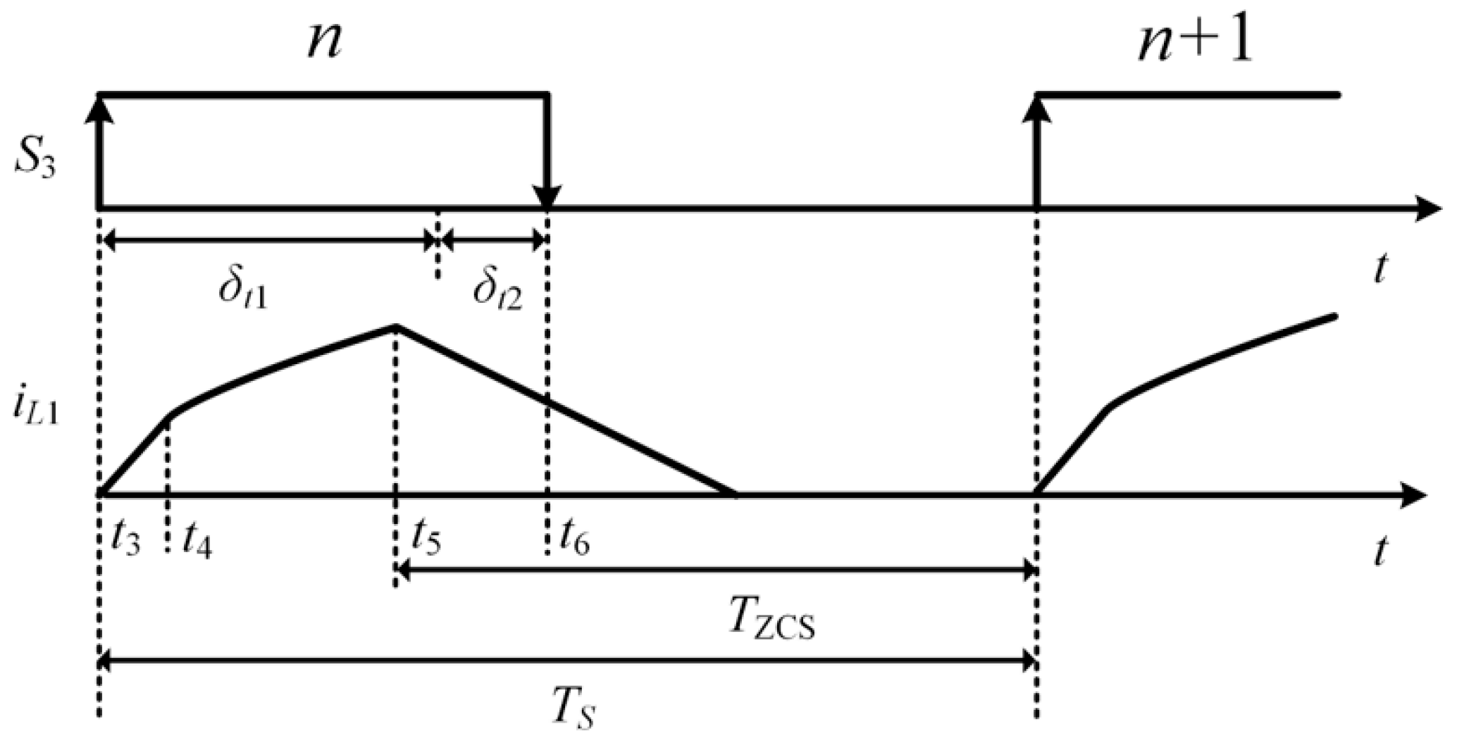
To realize the ZCS turn-on for (S3, S4), it is necessary to ensure that the currents through L1 and L2 decline to zero before S3 and S4 are turned on in the next switching period. According to (5) and (15), iL1max > iL2max. Therefore, as long as iL1 declines to zero before S3 is activated, S3 can realize ZCS turn-on, subsequently enabling S4 to also achieve ZCS turn-on.
As shown in Figure 5, the duration of the current in L1 declines to zero should be less than or equal to Tzcs, which can be expressed by the following:
where VD is the forward voltage of the diode, and Ts is the switching period. For a switching frequency of fs, Ts =1/fs. Tzcs is the duration within which the auxiliary switches can achieve ZCS turn-on.

Figure 5.
Pseudo-ZCS turn-on condition of the auxiliary switches.
3.2. Number of Components and Soft-Switching Action
Table 1 compares the number of components and their soft-switching performance. The key findings are as follows: (1) The proposed inverter employs the fewest auxiliary components relative to [22,23,24], leading to lower hardware costs and enhanced power density and reliability. (2) In the referenced works [22,23,24], auxiliary switches (S3, S4) achieve pseudo ZVS turn-off. In contrast, the proposed inverter’s auxiliary switches attain true ZVS turn-off, thereby significantly reducing turn-off losses.

Table 1.
Number of components and soft-switching action.
3.3. Voltage and Current Stress of Components
Table 2 provides a comparative analysis of the voltage and current stresses on the switches. Components that are not present in a particular topology are indicated with dashes. The main points from the table are as follows:
Table 2.
Electrical stress comparison.
- (1)
- The proposed inverter and the inverter in [22] utilize the fewest switches compared to those in [23,24], which simplifies control and reduces hardware costs;
- (2)
- The voltage stress on all switches in both the proposed inverter and those in [22,23,24] is constrained to the DC power supply E;
- (3)
- (S1, S2) in the proposed inverter and those in [22,23,24] experience current stress limited to the peak output current iamax;
- (4)
- The auxiliary switches in the proposed inverter are subjected to the lowest current stress. This stress can be further minimized by increasing the auxiliary resonant inductance L and decreasing the auxiliary resonant capacitance C.
In summary, the voltage stress on all switches and the current stress on the main switches (S1, S2) in the proposed inverter are on par with those in [22,23,24]. However, the proposed inverter shows advantages in terms of lower current stress on auxiliary switches and a reduced number of auxiliary components.
4. Parameter Design
Considering the input DC voltage E and the maximum output load current iamax, the design parameters must adhere to the following criteria:
- (1)
- To facilitate soft-switching, the conditions specified in Equations (18)–(20) must be met;
- (2)
- The change rate of voltage should be constrained to a set limit (dv/dt)set, and similarly, the current change rate should remain within the set limit (di/dt)set. These conditions can be mathematically represented as follows:
- (3)
- To optimize the efficiency of the system, this paper tries to minimize the circulation loss of inductance current. The total circulation loss is as follows:
As detailed in (23), meeting these parameters requires minimizing capacitors (C) and inductors (L). This reduction is crucial to decrease circulating losses and improve the overall efficiency of the system. According to (15), to mitigate the current stress on the auxiliary switches, it is essential to prioritize selecting the smallest feasible capacitance (C).
Therefore, the optimal design involves carefully balancing these components to achieve the desired soft-switching performance while minimizing losses and stress on the auxiliary switches. By appropriately selecting smaller values for (C) and (L), the system can operate more efficiently, with reduced thermal and electrical stress on its components.
5. Experimental Results
To validate the correctness of the analysis presented, a prototype with a capacity of 3 kW and operating at 16 kHz was constructed. The specific components and their parameters are detailed in Table 3.
Table 3.
Components and parameters of the prototype.
5.1. Waveforms Evaluation
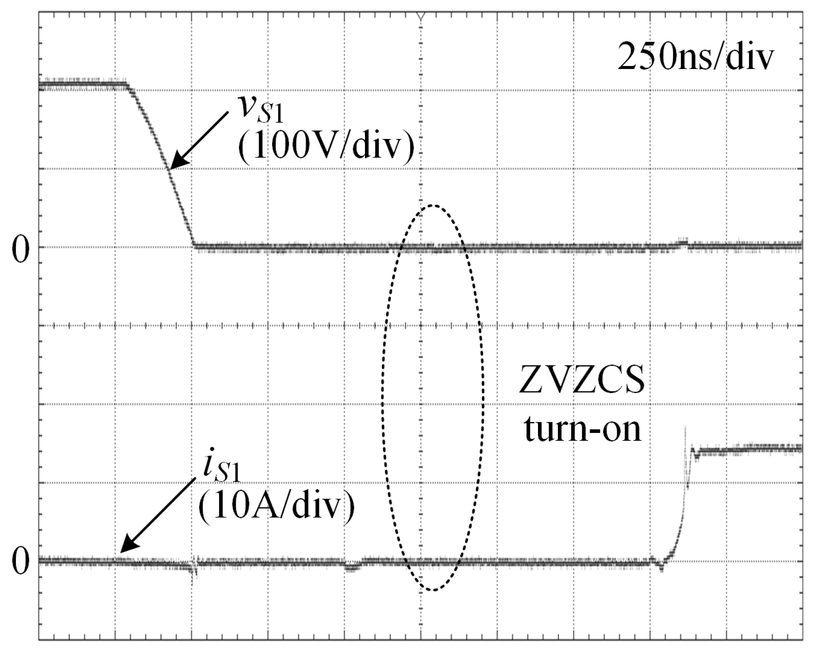
Figure 6 presents the turn-on waveforms of the main switch S1. From Figure 6, it is apparent that both the voltage and current of S1 are zero just before the switch is turned on. This condition ensures that S1 achieves ZVZCS during turn-on, thereby minimizing switching losses.

Figure 6.
Turn-on waveforms of the main switch S1.
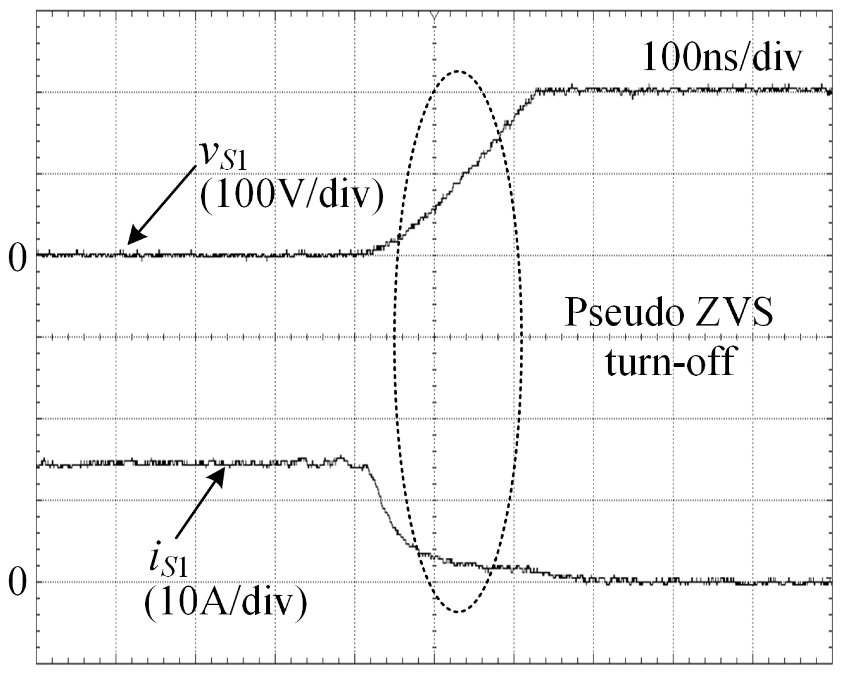
The turn-off waveforms of S1 are shown in Figure 7. The voltage across S1 can be seen to rise gradually from zero when S1 transitions from on to off. This slow rise in voltage indicates a pseudo-ZVS turn-off, which helps in reducing the turn-off losses and prolongs the lifespan of the switch by minimizing the stress during the transition.
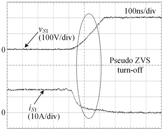
Figure 7.
Turn-off waveforms of the main switch S1.
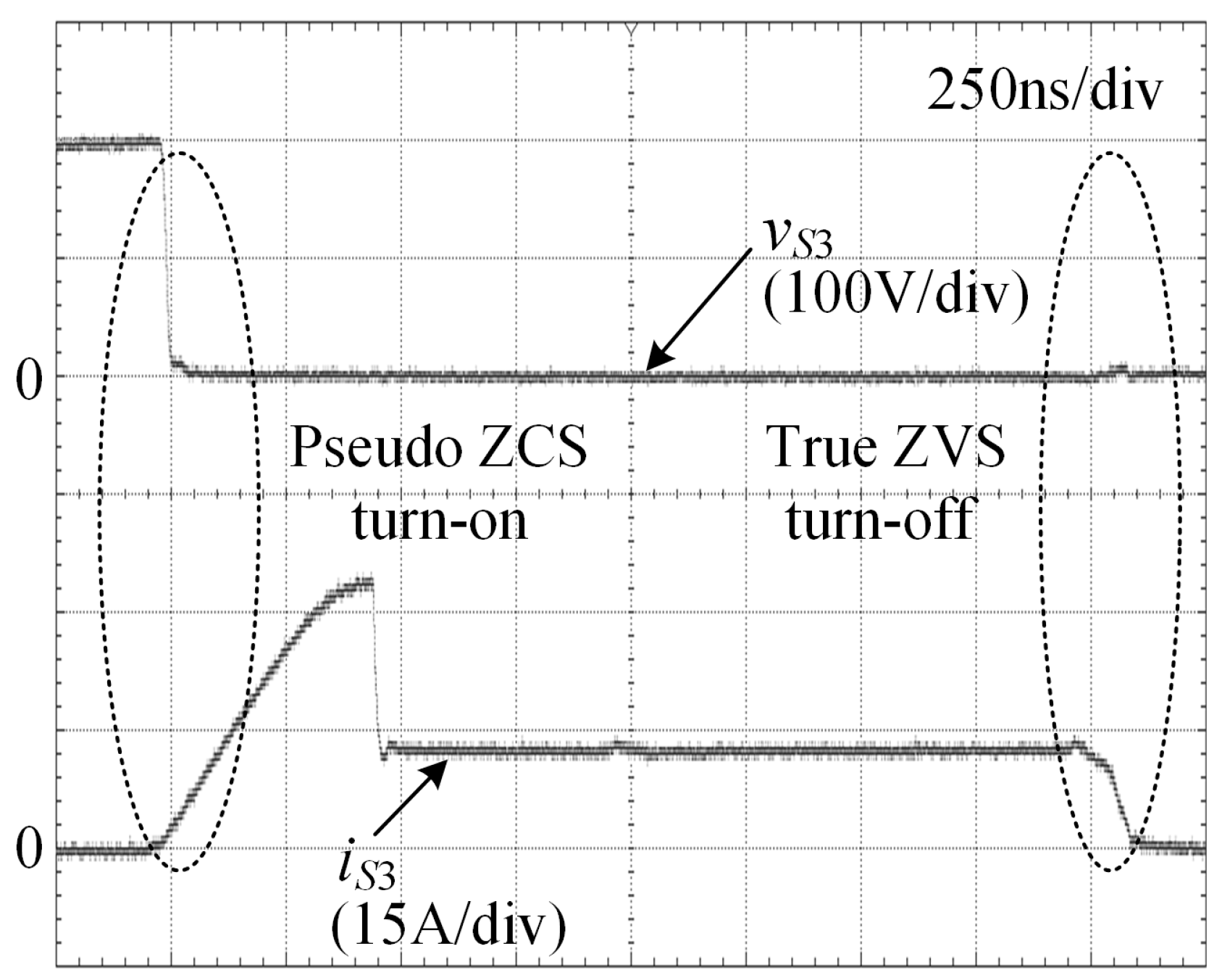
Figure 8 illustrates the voltage and current waveforms of S3 during both turn-on and turn-off transitions. The figure shows that the current through S3 increases at a lower rate, which is indicative of a pseudo-ZCS turn-on. Additionally, the voltage across S3 remains at zero during the turn-off transition, demonstrating a true ZVS turn-off. These conditions help in significantly reducing the switching losses and improving the overall efficiency of the inverter.
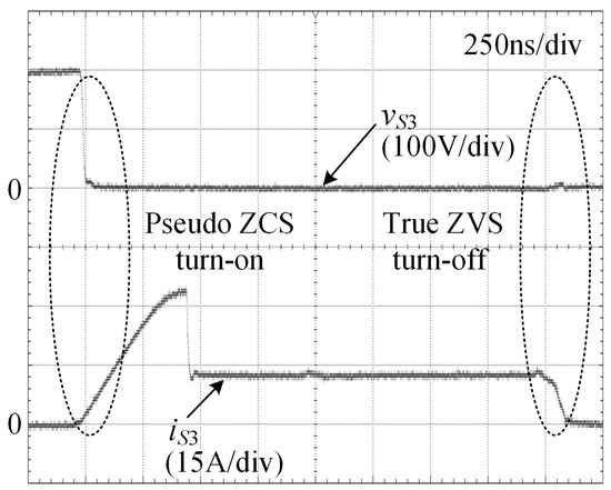
Figure 8.
The experimental waveforms of auxiliary switch S3.
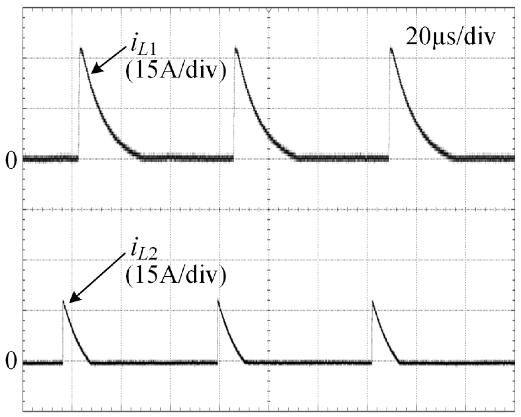
Figure 9 depicts the current waveforms of L1 and L2. From Figure 9, it is evident that the currents through L1 and L2 decay rapidly to zero within each switching cycle. This rapid decline ensures that S3 and S4 can achieve a pseudo-ZCS turn-on, which is crucial for minimizing switching losses. The iL1 and iL2 exhibit an exponential decay pattern, which can be attributed to the inherent parasitic resistances within the circuit components.
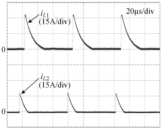
Figure 9.
The experimental waveforms of auxiliary resonant inductors.
5.2. Efficiency Comparison
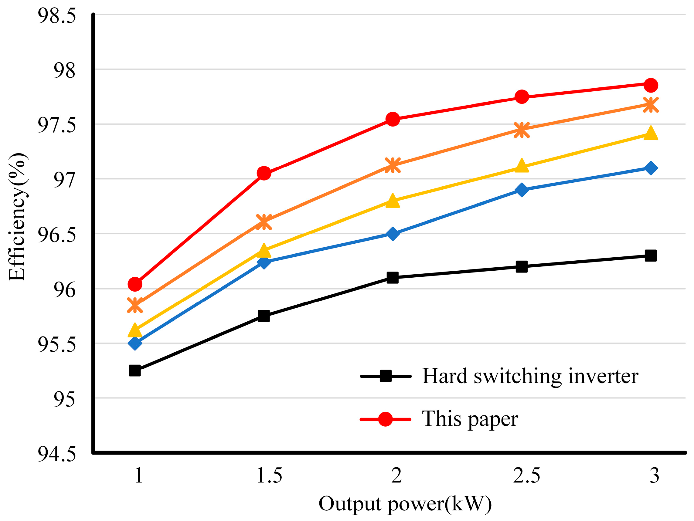
Figure 10 compares the efficiency of the proposed soft-switching inverter with those of inverters presented in [22,23,24] and a conventional hard-switching inverter. The data reveal that the proposed inverter achieves an efficiency of 97.8% at an output power of 3 kW. This efficiency is significantly higher than that of other inverters within 1–3 kW. The superior efficiency of the proposed inverter is primarily due to the simplification of the commutation process, which reduces the associated switching losses. Additionally, the implementation of soft-switching techniques in the proposed inverter further enhances its efficiency by lowering the thermal and electrical stresses on the components. Overall, the experimental results validate the effectiveness of the proposed inverter design in achieving high efficiency and reliable performance through reduced switching losses and enhanced soft-switching capabilities.

Figure 10.
Efficiency curves. (Efficiency curves of inverters from [22,23,24], represented by blue, yellow, and brown lines, respectively).
6. Conclusions
This paper introduces a novel soft-switching inverter topology. From theoretical analysis and experimental research, the following conclusions can be drawn:
- (1)
- The proposed topology features a simplified structure with fewer components and reduced operating modes. This simplification not only lowers the overall cost but also enhances the inverter’s performance by making it more efficient and reliable;
- (2)
- All switches are capable of achieving soft-switching. Specifically, while auxiliary switches in [22,23,24] manage the pseudo-ZVS turn-off, the auxiliary switches in the proposed inverter achieve a true ZVS turn-off. This true ZVS turn-off significantly reduces switching losses and improves the overall efficiency and longevity of the switches by minimizing stress during transitions;
- (3)
- When compared to the ARCP inverters detailed in [22,23,24], the proposed inverter demonstrates superior transmission efficiency. This improvement is primarily due to the enhanced soft-switching capabilities and the reduced number of components, which collectively contribute to lower power losses and higher operational efficiency.
Author Contributions
Writing—original draft, D.D.; Supervision, H.Z. All authors have read and agreed to the published version of the manuscript.
Funding
This research received no external funding.
Data Availability Statement
Data are available on request from the authors.
Conflicts of Interest
The authors declare no conflicts of interest.
References
- Chu, E.; Kang, Y.; Zhang, P.; Wang, Z.; Zhang, T. An SVPWM method for parallel resonant DC-Link inverter with the smallest loss in the auxiliary commutation circuit. IEEE Trans. Power Electron. 2022, 37, 1772–1787. [Google Scholar] [CrossRef]
- Chen, Y.; Xu, D. Review of Soft-Switching Topologies for Single-Phase Photovoltaic Inverters. IEEE Trans. Power Electron. 2022, 37, 1926–1944. [Google Scholar] [CrossRef]
- Li, R.; Xu, D. A zero-voltage switching three-phase inverter. IEEE Trans. Power Electron. 2014, 29, 1200–1210. [Google Scholar]
- Kedarisetti, J.; Mutschler, P. A motor-friendly quasi-resonant DC-link inverter with lossless variable zero-voltage duration. IEEE Trans. Power Electron. 2012, 27, 2613–2622. [Google Scholar] [CrossRef]
- Jafar, J.; Fernandes, B. A new quasi-resonant DC-link PWM inverter using single switch for soft switching. IEEE Trans. Power Electron. 2002, 17, 1010–1016. [Google Scholar] [CrossRef]
- Wang, Q.; Guo, G.; Wang, Y.; Chen, J. An Efficient Three-Phase Resonant DC-Link Inverter with Low Energy Consumption. IEEE Trans. Power Electron. 2021, 36, 702–715. [Google Scholar] [CrossRef]
- Divan, D. The resonant DC link converter-a new concept in static power conversion. IEEE Trans. Ind. Appl. 1989, 25, 317–325. [Google Scholar] [CrossRef]
- Chu, E.; Zhang, T.; Wang, Z. Auxiliary resonant commutated pole soft-switching inverter with simple topology. J. Power Electron. 2022, 22, 198–209. [Google Scholar] [CrossRef]
- McMurray, W. Resonant snubbers with auxiliary switches. In Proceedings of the Conference Record of the IEEE Industry Applications Society Annual Meeting, San Diego, CA, USA, 1–5 October 1989; pp. 289–834. [Google Scholar]
- Doncker, R.W.D.; Lyons, J.P. The auxiliary resonant commutated pole converter. In Proceedings of the Conference Record of the 1990 IEEE Industry Applications Society Annual Meeting, Seattle, WA, USA, 7–12 October 1990; pp. 1228–1235. [Google Scholar]
- Lai, J.; Young, S.; Ott, J.; McKeever, J.; Fang, Z. A delta-configured auxiliary resonant snubber inverter. IEEE Trans. Ind. Appl. 1996, 32, 518–525. [Google Scholar]
- Lai, J. Practical design methodology of auxiliary resonant snubber inverters. In Proceedings of the PESC Record. 27th Annual IEEE Power Electronics Specialists Conference, Baveno, Italy, 23–27 June 1996; pp. 432–437. [Google Scholar]
- Yamamoto, H.; Kaneda, M.; Nakaoka, M. Three-phase soft-switching inverter resonant with unique resonant snubbers. In Proceedings of the IEEE 1999 International Conference on Power Electronics and Drive Systems, Hong Kong, China, 27–29 July 1999; pp. 1078–1083. [Google Scholar]
- Lai, J.; Zhang, J.; Yu, H.; Kouns, H. Source and load adaptive design for a high-power soft-switching inverter. IEEE Trans. Power Electron. 2006, 21, 1667–1675. [Google Scholar] [CrossRef]
- Russi, J.; Martins, M.; Hey, H. Coupled-filter-inductor soft-switching techniques: Principles and topologies. IEEE Trans. Ind. Electron. 2008, 55, 3361–3373. [Google Scholar] [CrossRef]
- Yu, W.; Lai, J.; Park, S. An improved zero-voltage switching inverter using two coupled magnetics in one resonant pole. IEEE Trans. Power Electron. 2010, 25, 952–961. [Google Scholar]
- Yuan, X.; Barbi, I. Analysis, designing, and experimentation of a transformer-assisted PWM zero-voltage switching pole inverter. IEEE Trans. Power Electron. 2000, 15, 72–82. [Google Scholar] [CrossRef]
- Inaba, C.; Yamazaki, T.; Yoshida, M.; Hiraki, E.; Konishi, Y.; Nakaoka, M. Three phase soft switching inverter with pulse current transformer-assisted resonant snubbers. IEEE Int. Conf. Ind. Electron. 2001, 2, 1106–1111. [Google Scholar]
- Turzynski, M.; Chrzan, P.; Kolincio, M.; Burkiewicz, S. Quasi resonant DC-link voltage inverter with enhanced zero-voltage switching control. In Proceedings of the 19th European Conference on Power Electronics and Applications (EPE’17 ECCE Europe), Warsaw, Poland, 11–14 September 2017; pp. 1–8. [Google Scholar]
- Wang, Q.; Wang, Y. Research on a novel high-efficiency three-phase resonant pole soft-switching inverter. IEEE Trans. Power Electron. 2021, 36, 5845–5857. [Google Scholar] [CrossRef]
- Chu, E.; Wu, M.; Huang, L.; Hou, X.; Zhang, H. Research on a novel modulation strategy for auxiliary resonant commutated pole inverter with the smallest loss in auxiliary commutation circuits. IEEE Trans. Power Electron. 2014, 29, 1103–1117. [Google Scholar]
- Chu, E.; Zhang, X.; Sun, Q.; Li, S.; Xiong, H.; Yang, X. Three-phase double auxiliary resonant commutated pole inverter topology and analysis of its working principle. IET Power Electron. 2016, 9, 1536–1545. [Google Scholar] [CrossRef]
- Chu, E.; Zhang, X.; Huang, L. Research on a novel modulation strategy for double auxiliary resonant commutated pole soft-switching inverter with the shunt dead time. IEEE Trans. Power Electron. 2016, 31, 6855–6869. [Google Scholar] [CrossRef]
- Chu, E.; Chen, Z.; Xie, H.; Zhang, H. Modified double auxiliary resonant commutated pole inverter and its modulation strategy. IEEE J. Emerg. Sel. Topics Power Electron. 2020, 8, 4467–4481. [Google Scholar] [CrossRef]

Disclaimer/Publisher’s Note: The statements, opinions and data contained in all publications are solely those of the individual author(s) and contributor(s) and not of MDPI and/or the editor(s). MDPI and/or the editor(s) disclaim responsibility for any injury to people or property resulting from any ideas, methods, instructions or products referred to in the content. |
© 2024 by the authors. Licensee MDPI, Basel, Switzerland. This article is an open access article distributed under the terms and conditions of the Creative Commons Attribution (CC BY) license (https://creativecommons.org/licenses/by/4.0/).