Article

Structural and Compositional Analysis of CZTSSe Thin Films by Varying S/(S+Se) Ratio

by
Mohamed Yassine Zaki
,
Florinel Sava
,
Iosif Daniel Simandan
,
Claudia Mihai
and
Alin Velea
*
National Institute of Materials Physics, Atomistilor 405A, 077125 Magurele, Romania
*
Author to whom correspondence should be addressed.
Energies 2024, 17(15), 3684; https://doi.org/10.3390/en17153684
Submission received: 16 June 2024 / Revised: 15 July 2024 / Accepted: 18 July 2024 / Published: 26 July 2024
(This article belongs to the Special Issue Advances on Solar Energy Materials and Solar Cells)

Abstract

:
The development of kesterite (Cu2ZnSn(S,Se)4, CZTSSe) thin films for photovoltaic applications is highly necessary, given their composition of Earth-abundant, environmentally friendly elements and their compatibility with established photovoltaic technologies. This study presents a novel synthesis approach for CZTSSe films with varied S/(S+Se) ratios, ranging from 0.83 to 0.44, by a two-step magnetron sputtering deposition/annealing process. The first step consists in an initial deposition of stacked Mo/SnS2/Cu layers, which, upon thermal treatment in a sulfur atmosphere, were transformed into Cu2SnS3 (CTS) films. In the second step, further deposition of ZnSe and subsequent annealing in a tin and selenium atmosphere resulted in the formation of a CZTSSe phase. These processes were optimized to fabricate high-quality and single-phase CZTSSe films, thereby mitigating the formation of secondary phases. Characterization techniques, including scanning electron microscopy, demonstrated a clear correlation between decreased S/(S+Se) ratios and enhanced film densification and grain size. Moreover, grazing incidence X-ray diffraction and Raman spectroscopy confirmed a compositional and structural transition from close to CZTS to nearly a CZTSe phase as the S/(S+Se) ratios decreased. This study advances kesterite-based solar cell technology by enhancing the structural properties and crystallinity of the absorber layer, necessary for improving photovoltaic performance.

1. Introduction

Kesterite thin films have garnered significant attention in the field of photovoltaics due to their potential as absorber layers in thin film solar cells (TFSC) [1]. These materials exhibit advantageous properties such as Earth abundance, non-toxicity, and optimal bandgap for solar energy conversion [2]. The kesterite structure, characterized by a tetragonal crystal lattice belonging to the space group I-4, provides favorable electronic properties for efficient photovoltaic performance [3]. The kesterite family of materials includes copper zinc tin sulfide (Cu2ZnSnS4, CZTS) [4], copper zinc tin selenide (Cu2ZnSnSe4, CZTSe) [5], and their mixed compound, copper zinc tin sulfoselenide (Cu2ZnSn(S,Se)4, (CZTSSe) [6]. CZTSSe combines both sulfur and selenium, offering a tunable composition that balances the properties of CZTS and CZTSe, making it particularly attractive for photovoltaic applications [7]. In the CZTSSe structure, Cu atoms occupy the 2a and 2c sites, Zn atoms occupy the 2d sites, and tin (Sn) atoms are located at the 2b sites. The chalcogen atoms, S and Se, are positioned at the 8 g sites, which are tetrahedrally coordinated by the metal atoms [8].
Over the years, comprehensive research has been dedicated to the synthesis of CZTSSe thin films, aiming to optimize their properties for enhanced solar cell efficiency. Various deposition techniques have been employed to precisely control the sulfur to selenium (S/Se) ratio in CZTSSe films [9], including vacuum-based methods such as magnetron sputtering [10], thermal evaporation [11], and pulsed laser deposition [12], as well as solution-based techniques like sol-gel [13], and electrodeposition [14]. These methods offer distinct advantages in terms of scalability, control over composition, and film quality, contributing to the versatility and applicability of CZTSSe materials in photovoltaic devices. Studies have shown that adjusting the S/Se ratio in CZTSSe films can significantly impact their morphological, structural and optical properties, influencing overall solar device performance [15]. For instance, higher sulfur content tends to increase the band gap, which can improve open-circuit voltage but may reduce the absorption of lower energy photons [16]. Conversely, increasing selenium content often enhances carrier mobility and absorption but can lower the band gap [17]. The substitution of S with Se in the lattice leads to an increase in lattice parameters due to the larger atomic radius of Se compared to S, resulting in an expansion of the unit cell. This substitution also affects the bond lengths within the lattice; Se forms longer bonds with the metal atoms compared to S, which influences the overall structural and electronic properties of the material [18,19]. Precise control over the S/Se ratio allows for enhanced photovoltaic performance by tailoring the optical and electrical properties of CZTSSe. applications. Recently, CZTSSe solar cells have been shown to achieve a power conversion efficiency of ~14.6% [20].
However, several issues were observed in previous studies on the synthesis of CZTSSe thin films with a controlled S/Se ratio. One of the main difficulties is mitigating the formation of secondary phases such as ZnSe and intrinsic defects like CuSn, where copper atoms occupy tin sites [14], which can significantly affect the electrical properties and stability of the material. Additionally, achieving a uniform distribution of sulfur and/or selenium throughout the film remains a significant challenge, often resulting in compositional inhomogeneity, as observed by Woo et al. [21]. In their study, irregularities in the distribution of the elements arises from the inconstant Se vapor pressure during the selenization process, leading to Se grading within the CZTSSe absorber layer which produces a high short-circuit current density. Furthermore, Kim et al., in their study of CZTSSe films obtained from DC-sputtered metallic precursors (Sn/Cu/Zn) on a molybdenum-coated soda-lime glass substrate, reported the presence of non-uniform morphologies and secondary phases, including the formation of a thick Mo(S,Se)2 layer at the interface of Mo/CZTSSe that leads to poor carrier collection at the back contact [22]. Finding solutions to these issues is crucial for advancing the development of high-performance CZTSSe thin films.
In this paper, we address the challenges in synthesizing CZTSSe thin films by using a two-step magnetron sputtering deposition followed by a controlled annealing process. We first prepared CTS precursor films from an annealed Cu/SnS2 stack in a sulfur atmosphere. Then, ZnSe is deposited, and the films are further annealed in a tin and selenium atmosphere. By varying the annealing parameters, we can precisely control the S/(S+Se) ratios, ensuring uniform sulfur and selenium distribution and suppressing the formation of unwanted secondary phases. This method overcomes the issues of previous techniques, leading to improved film quality and advancing the potential of CZTSSe in photovoltaic applications.

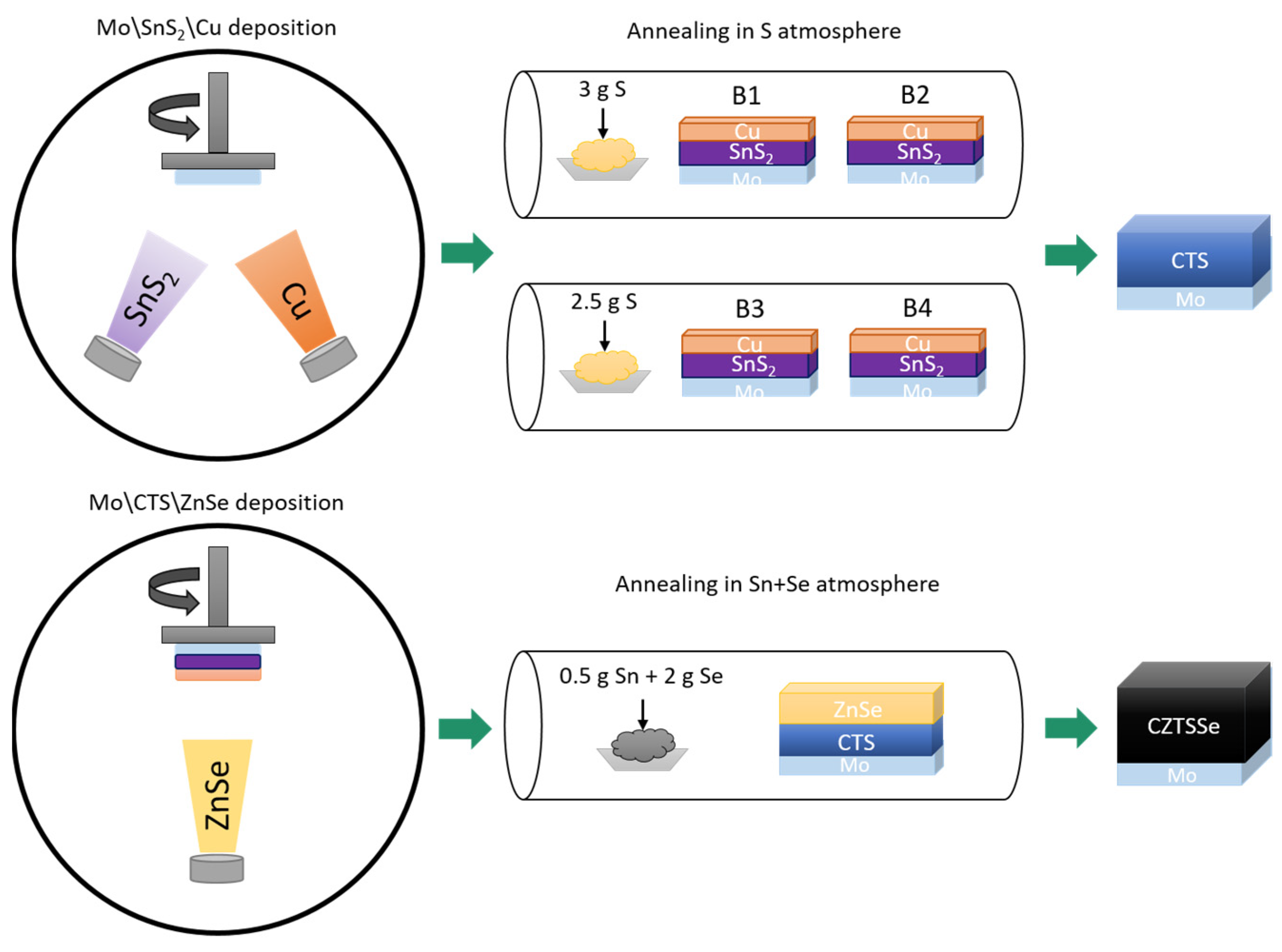
2. Materials and Methods
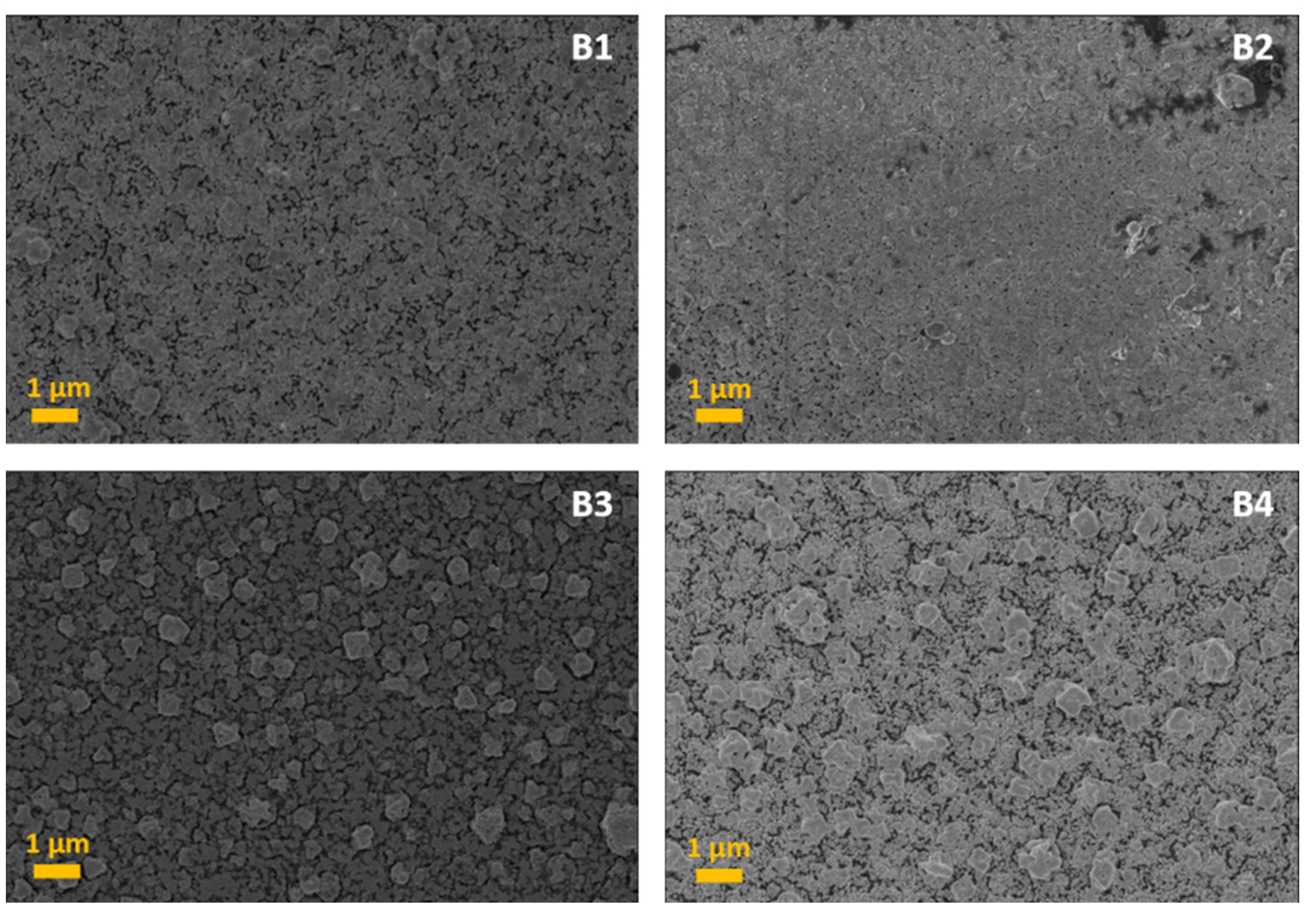
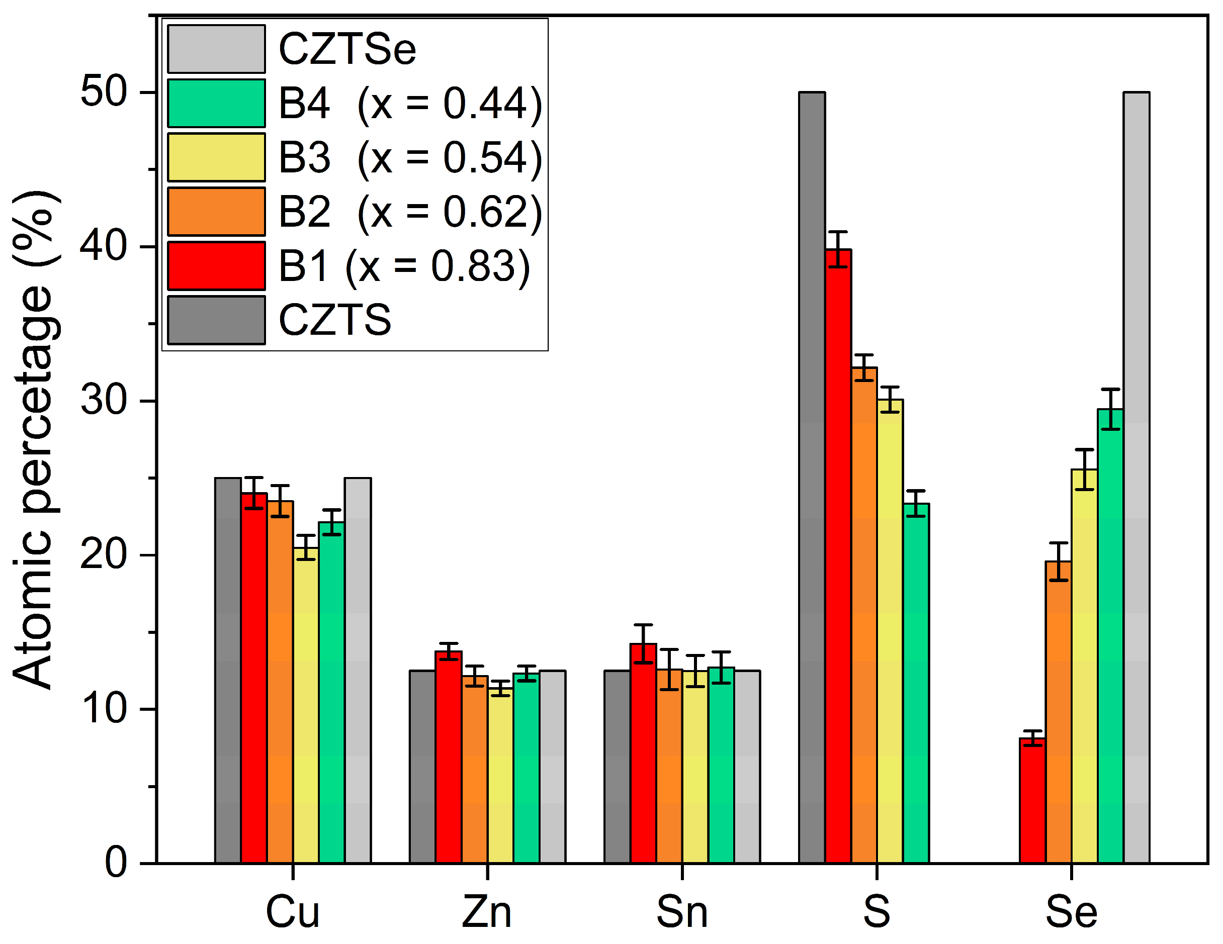
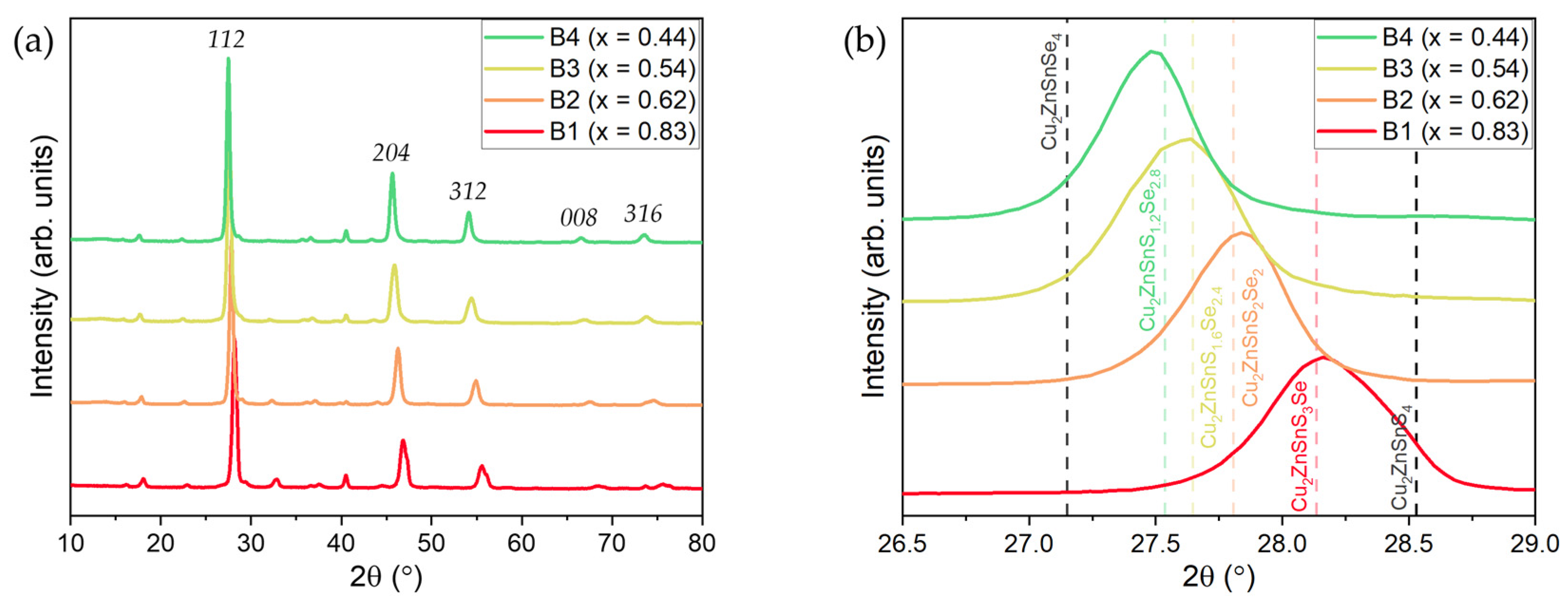
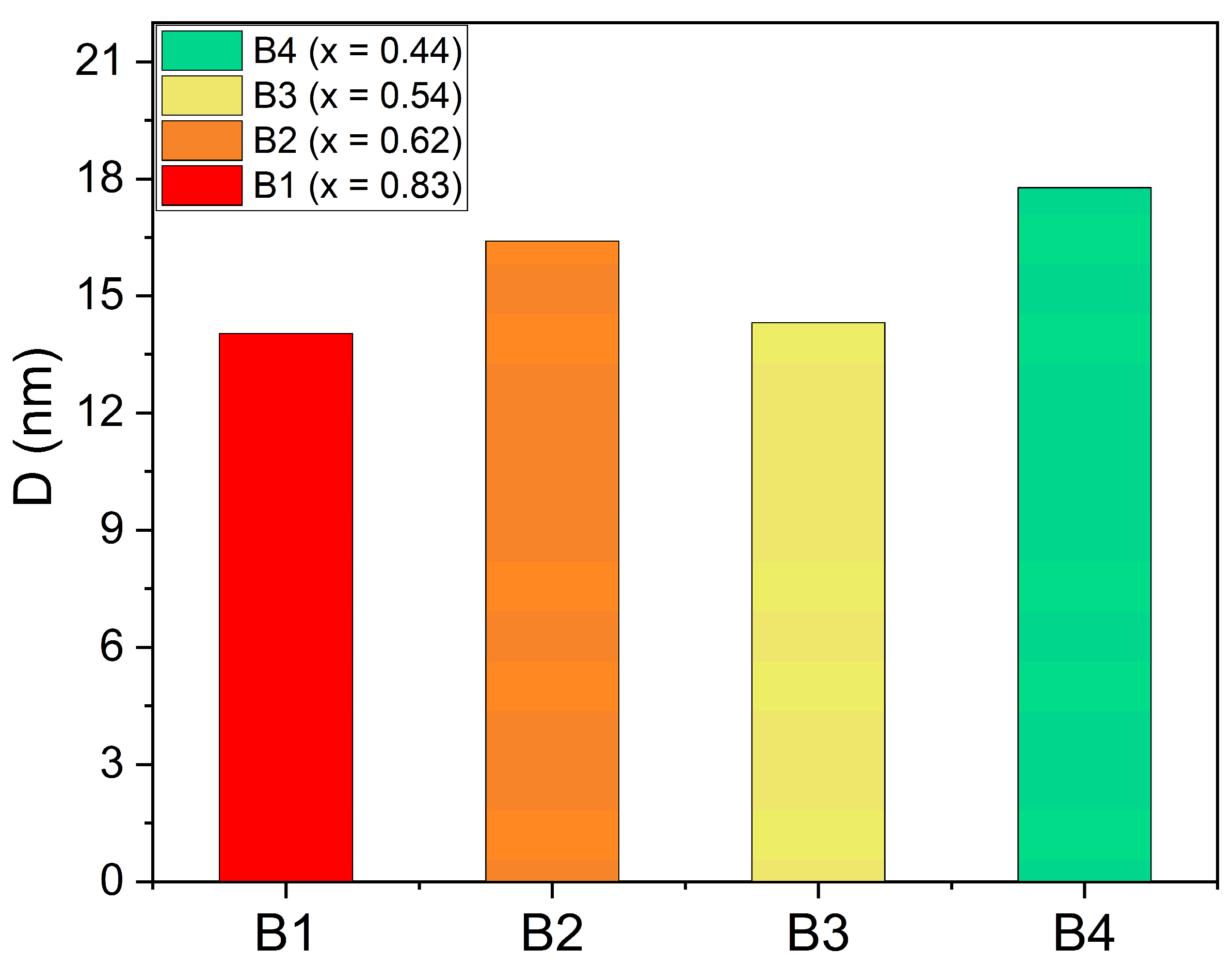
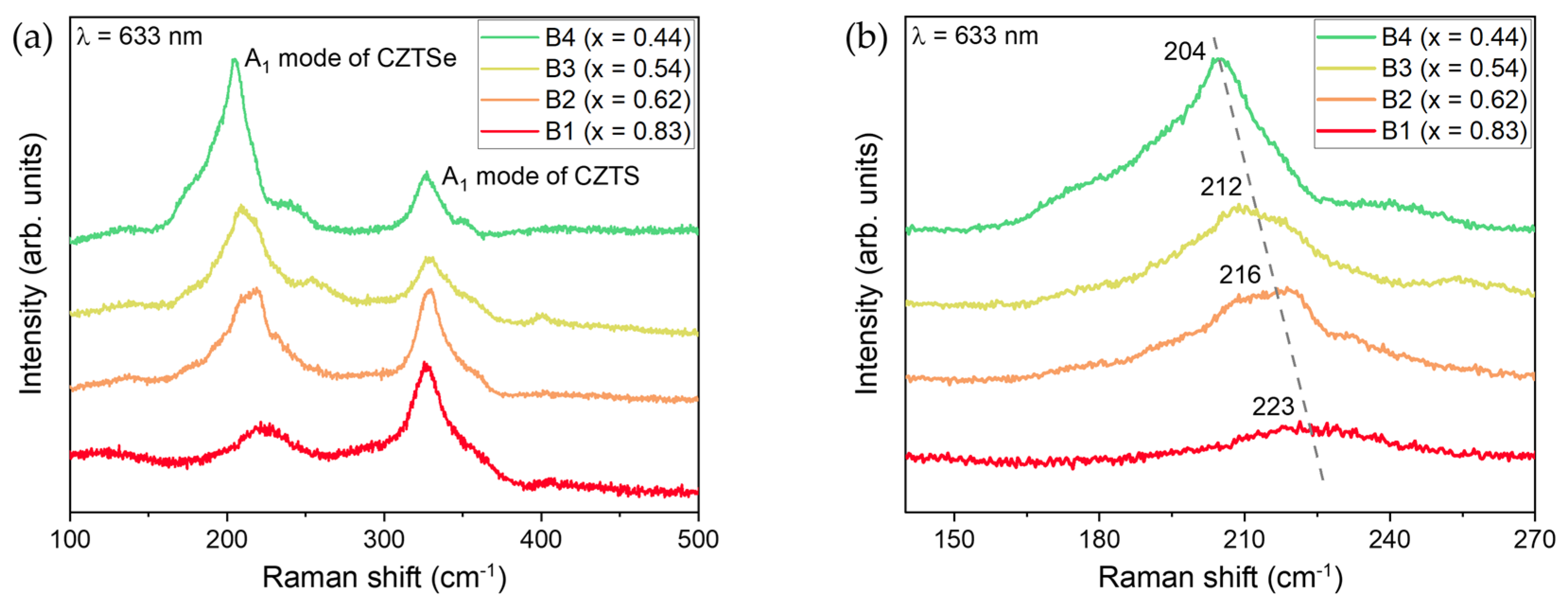
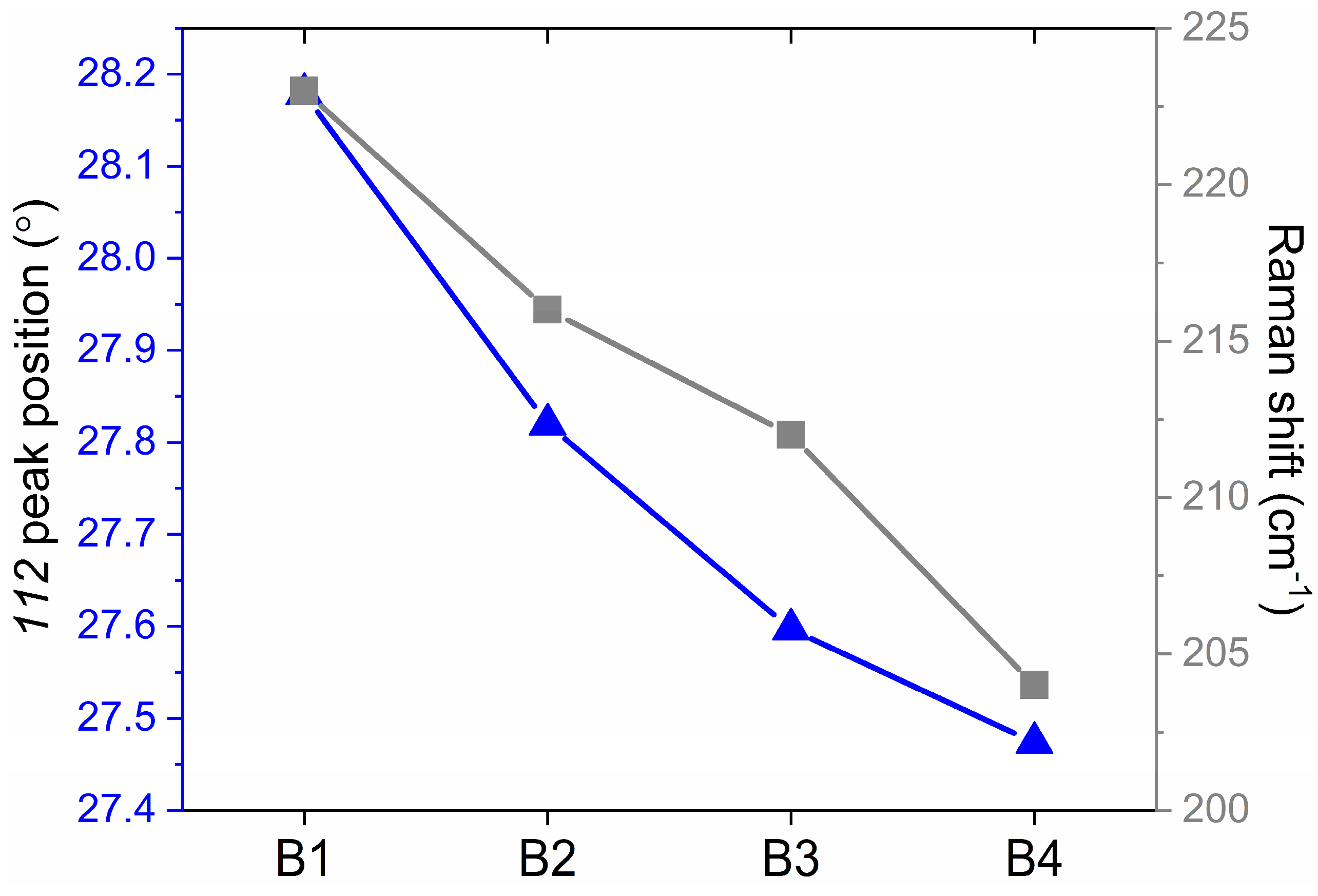
The CZTSSe thin films were deposited onto molybdenum (Mo)-coated soda-lime glass (SLG) substrates using magnetron sputtering. The first step started with four similar Mo/SnS2/Cu stacks, where a SnS2 layer was initially sputtered, followed by a copper film on top of the SnS2 layer. The stacks were prepared at room temperature using 3G Circular Magnetrons (Gencoa, Liverpool, UK), and RF sources (T&C Power Conversion AG 0313, Rochester, NY, USA) for both the SnS2 and Cu targets. The depositions used 2-inch diameter sputtering targets of SnS2 and Cu (99.99% purity, Mateck Gmbh, Jülich, Germany). The chamber pressure was maintained at 1.1 × 10⁻⁵ Torr before deposition and 5 × 10⁻³ Torr during deposition in an argon environment with a flow of 30 SCCM. The deposition was performed without breaking the vacuum, with substrates placed 12 cm from the sputtering targets and continuously rotated for uniform deposition. A 5-min pre-sputtering was performed for each target to remove surface impurities. The sputtering rates were optimized using Inficon Q-pod quartz crystal monitor (Bad Ragaz, Switzerland). The power used to achieve a 0.51 Å/s rate was 19 W for SnS2, with a power of 31 W for Cu resulting in a rate of at 0.24 Å/s. The sputtering times were adjusted to achieve the desired thicknesses: 400 nm for SnS2, and 100 nm for Cu. These deposition parameters were carefully selected and optimized based on previous experiments. The rates used ensured uniform film growth and good adhesion to the substrate, which are important for obtaining high-quality films. Additionally, the thicknesses used in the stack were selected in order to obtain the desired stoichiometry in the final CZTSSe films after the annealing process. These values were optimized to provide the intended results in our specific setup and conditions. The as-deposited stacked films were annealed in a quartz tube using a GSL 1600X tubular furnace with a 10 SCCM argon flow. CTS films with different compositions were obtained by annealing the four stacks at a fixed temperature of 350 °C for 5 min, using a boat with 3 g of sulfur powder for samples B1 and B2, with B1 placed closer to the boat, and a boat with 2.5 g of sulfur powder for samples B3 and B4, with B3 placed closer to the boat. The S/(S+Se) ratios were controlled based on the amount of sulfur used in the first annealing process when the CTS precursors were synthesized. Post-annealing, a 150 nm ZnSe layer was sputtered onto the CTS thin films, applying 41 W for a deposition rate of 0.50 Å/s. A second heat treatment (using the same annealing parameters for the four samples) was conducted on the four Mo/CTS/ZnSe stacks with 0.5 g of Sn and 2 g of Se powders at 550 °C for 30 min, using two boats of Sn and Se powders upstream in the Ar flow. The final films were labeled B1, B2, B3, and B4 with a decreasing S/(S+Se) ratios. A schematic of the deposition and annealing process is presented in Figure 1. The crystalline structure of the thin films was analyzed using a Rigaku SmartLab X-ray diffractometer (Tokyo, Japan) with an incidence angle of 0.75°, Cu Kα (λ = 1.54187 Å) radiation, and a HyPix-3000 2D Hybrid Pixel Array Detector (Rigaku Corporation, Tokyo, Japan) in 0D mode for grazing incidence X-ray diffraction (GIXRD) measurements. The LabRAM HR Evolution Raman spectrometer from HORIBA Jobin-Yvon (Palaiseau, France), with a confocal Olympus 100× microscope (Tokyo, Japan) and a He–Ne laser (633 nm excitation), was used to support the GIXRD results. Surface morphology and compositional analysis were performed using a Gemini 500 Field Emission Scanning Electron Microscope (FE-SEM) from Zeiss, Oberkochen, Germany provided with an energy dispersive X-ray (EDX) spectrometer from Bruker (Billerica, MA, USA).

3. Results

Figure 2 presents four scanning electron microscope (SEM) images of the CZTSSe samples, providing insights into their surface morphology. A homogeneous surface morphology is observed in all samples, indicative of uniform film deposition and crystallization. Notably, samples B3 and B4 exhibit larger grain sizes compared to the B1 and B2 films, suggesting a potential correlation between the S/(S+Se) ratio and grain growth kinetics. The presence of larger grains in samples B3 and B4 may indicate enhanced crystallinity, possibly influenced by variations in the S/(S+Se) ratio [23]. Additionally, no cracks or voids were observed in any of the films, indicating good film quality and adhesion to the Mo substrate.
The elemental composition and atomic ratios of the CZTSSe films were analyzed through energy-dispersive X-ray spectroscopy (EDS) measurements and are illustrated in Figure 3 and Table 1. For each sample, EDS analysis was conducted on several areas, typically three to five different zones, and then an average of the measured values was calculated. The results from these areas showed very consistent elemental distributions. This method ensures the homogeneity of the element distribution and composition within the samples. The gray and dark gray bars in Figure 3 represent the ideal stoichiometry for pure CZTSe and CZTS phases with the following elemental compositions: Cu = 25%, Zn = 12.5%, Sn = 12.5%, and Se = 50% for CZTSe, and Cu = 25%, Zn = 12.5%, Sn = 12.5%, and S = 50% for CZTS. These ideal compositions were included as references for comparison with our CZTSSe samples. This allows for a clearer understanding of how the actual compositions of the synthesized samples compare with the theoretical ideal compositions of CZTSe and CZTS.
All films exhibit a nearly stoichiometric composition closely resembling the expected Cu2ZnSn(S,Se)4 compound. The atomic percentages of each element in the four samples are close to the intended 25% of Cu, 12.5% of Zn, and 12.5% of Sn, and 50% for S+Se, respectively. Notably, differences among the samples are primarily observed in the S/(S+Se) ratio. Sample B1 exhibits a S-rich composition, with the highest sulfur content and lowest selenium content, which is close to the elemental composition of the CZTS phase [24]. The S/(S+Se) ratio for B1 is 0.83, indicating a predominantly sulfur-rich environment. As we progress through the samples, the sulfur content gradually decreases and selenium content increases. Sample B2 has a ratio of 0.62, B3 has a ratio of 0.54, and B4 has a ratio of 0.44, indicating a transition towards a selenium-rich composition, with sample B4 demonstrating the highest selenium content and lowest sulfur content, close to the atomic percentages characteristic of the CZTSe phase [18].
To investigate the compositional homogeneity of the samples, we performed EDS mapping. The results, shown in Figure 4, indicate that the distribution of Cu, Zn, Sn, S, and Se elements is uniform in the B2 sample. Similar uniform distributions were observed for samples B1, B3, and B4. Additionally, the detection of the Mo substrate during the EDS measurements suggests that the entire CZTSSe film thickness was probed. These results support our conclusion of a homogeneous and compact grain structure with well-distributed elements.
The X-ray diffraction (XRD) diffractograms of the four CZTSSe (B1, B2, B3, and B4) samples with varying S/(S+Se) ratios reveal distinctive patterns indicative of single-phase CZTSSe formation with no detectable secondary phases, as observed in Figure 5a. The diffraction peaks corresponding to the kesterite phase are observed at consistent positions across all samples, confirming the high crystallinity and purity of the CZTSSe films. The intensity and width of the diffraction peaks may vary slightly among the samples, reflecting differences in grain size and lattice strain resulting from variations in the S/(S+Se) ratio [8]. Overall, the XRD analysis provides evidence for the successful synthesis of single-phase CZTSSe thin films across the range of S/(S+Se) ratios investigated. Figure 5b is an enlarged view of the main CZTSSe peak, along with comparisons to ICDD cards of CZTS, CZTSe, and CZTSSe with different stoichiometries (dashed lines). It reveals changes in the crystalline structure of the CZTSSe samples. The diffraction patterns of the four samples fall within the range delineated by the ICDD cards of CZTS (00-026-0575) and CZTSe (04-019-1866). The shift in the 2θ peak suggests a continuous transition in the film composition as the sulfur to selenium ratio changes [25]. Sample B1, with x = 0.83, closely matches the ICDD card for Cu2ZnSnS3Se (04-023-9215), indicating a composition with a higher sulfur content and a lesser amount of selenium [26]. This composition leans toward the CZTS side of the range and suggests a structure that is rich in sulfur. Sample B2, with a S/(S+Se) = 0.62, aligns with the ICDD card for Cu2ZnSnS2Se2 (04-019-1851), showing a balance between sulfur and selenium [27]. This composition is closer to the middle of the CZTSSe range, reflecting a greater incorporation of selenium compared to B1. Sample B3, with a S/(S+Se) = 0.54, closely resembles the ICDD card for Cu2ZnSnS1.6Se2.4 (04-019-1850). This composition signifies a shift toward a higher selenium content and reduced sulfur content [28]. Finally, sample B4, with a S/(S+Se) = 0.44, approaches the ICDD card for Cu2ZnSnS1.2Se2.8 (04-019-1849), representing the film with the highest selenium content in the series. This composition is close to CZTSe, reflecting a shift toward a more selenium-rich structure. However, this specific structure was not reported in the literature, with few studies discussing similar Se-rich structures such as Cu2ZnSnSSe3 or Cu2ZnSnS0.8Se3.2 [29,30,31,32]. This observation suggests that there is still much to explore in the structural properties of CZTSSe films with varying S/(S+Se) compositions. This alignment with the various CZTSSe ICDD cards highlights the systematic control of film composition across the series, providing a basis for further investigation into the impact of varying the sulfur to selenium ratio on the physical and electronic properties of the films.
The average crystallite size of CZTS in each sample was calculated using the Scherrer equation. This estimation was based on the most intense (112) peak, taking into account the instrumental broadening [33]. Figure 6 presents the crystallite size of the four CZTSSe samples (B1, B2, B3, and B4), highlighting variations in the average crystallite size across the different compositions. Sample B1, with a S/(S+Se) value of 0.83, exhibits a crystallite size of 14.03 nm. This relatively lower size may be due to the higher sulfur content, which can result in more frequent nucleation sites and thus smaller crystallite sizes. In contrast, sample B2 (S/(S+Se) = 0.62) shows a higher crystallite size of 16.41 nm, indicating that the reduced sulfur content may allow the crystallites to grow larger due to less frequent nucleation. Sample B3, with an x value of 0.54, has a crystallite size of 14.32 nm, slightly smaller than B2. This suggests a balance between the effects of reduced sulfur and increased selenium content on crystallite growth. Finally, sample B4 (S/(S+Se) = 0.44) exhibits the largest crystallite size of 17.77 nm. This increase may be attributed to the significant reduction in sulfur content and corresponding increase in selenium content, which could facilitate larger crystallite growth due to fewer nucleation sites and potentially different growth dynamics in the film. Therefore, the fluctuations in crystallite size across the four samples may not be influenced by the varying proportions of sulfur and selenium solely; other factors likely contribute to the observed variations. Additionally, similar observations of crystallite size not strictly correlating with varying S/(S+Se) ratios have been reported in other studies [28,34], indicating that parameters beyond composition may contribute to the observed variations.
The Raman spectroscopy analysis of the four CZTSSe samples represented in Figure 7a shows a distinct trend in the shift and intensity of the two main peaks, reflecting changes in the composition of the films due to varying x = S/(S+Se) ratios. The Raman spectra display two distinct modes due to the existence of both S and Se atoms in the CZTSSe samples [35]. The first peak, observed around 220 cm−1, is related to the A1 mode of the CZTSe phase, which is known to have a prominent Raman peak at 196 cm−1 [36]. The second peak is located around 330 cm−1, which is characteristic of the A1 mode of the CZTS phase [37]. In sample B1, where x = 0.83, the first peak is observed at 223 cm−1 and a higher peak at 327 cm−1, indicating a composition closer to the CZTS end of the spectrum with a small initial peak and a dominant higher peak. As the x ratio decreases and the composition shifts towards a more selenium-rich phase, the intensity of the first peak increases, and its position shifts to lower values (Figure 7b), while the intensity of the second peak decreases [38]. This trend is observed in samples B2, B3, and B4, which show a continuous shift and increase in intensity of the first peak, while the second peak decreases in intensity. In sample B4, where x = 0.44, the first peak reaches its highest intensity and shifts towards 204 cm−1, while the second peak remains with low intensity. This progression in the Raman spectra suggests that as the x ratio decreases and the composition becomes richer in selenium, the vibrational modes associated with selenium-rich phases become more pronounced, resulting in the shift of the first peak to lower wavenumbers [19]. Meanwhile, the sulfur-rich phases become less prominent, as indicated by the decrease in intensity of the second peak. This trend is consistent with the samples transitioning from a S-rich to a Se-rich CZTSSe as the S/(S+Se) ratio changes. Additionally, it is noteworthy that no peaks corresponding to secondary phases were observed in the Raman spectra, affirming the high purity and single-phase nature of the CZTSSe thin films across all samples. The consistency between the Raman and XRD results reinforces the reliability of the structural characterization and provides evidence for the successful synthesis of CZTSSe thin films with precise compositional control.
Figure 8 presents a comparative analysis of the four CZTSSe samples (B1, B2, B3, and B4) illustrating the shifts in the most prominent XRD and Raman peaks. For the XRD 112 peak, in sample B1, the main peak is observed at 2θ = 28.17°, while in B2, it shifts slightly to 2θ = 27.81°. The trend continues with samples B3 and B4, where the main peak is observed at 2θ = 27.59° and 2θ = 27.47°, respectively. The progression across these samples shows a clear relationship between the S/(S+Se) ratio and the structural properties of the films [39]. As the selenium content increases (and the sulfur content decreases), the samples show a trend toward the CZTSe pattern. This trend reflects the transition from a sulfur-rich composition (higher x value) to a selenium-rich composition (lower x value), indicating lattice parameter expansion due to the larger atomic radius of selenium compared to sulfur [40]. Similarly, the Raman peak shift follows a parallel trend. As the sulfur content decreases from B1 to B4, the Raman peak also shifts to lower values [41]. This behavior can be attributed to the changes in the vibrational modes of the crystal lattice caused by the increasing selenium content, which affects the phonon frequencies [42]. The systematic decrease in the peak positions with increasing selenium content provides clear evidence of the structural and compositional changes occurring within the material, thus confirming the successful synthesis and varying compositions of the CZTSSe thin films.

4. Conclusions

In summary, a successful magnetron sputtering method was used to synthesize CZTSSe thin films with varying S/(S+Se) ratios through a two-step deposition and annealing process. SEM and EDS analyses revealed a homogeneous and compact grain structure with well-distributed elements. The S/(S+Se) ratios computed from EDS measurement exhibited an elemental composition variation from B1 (S-rich) to B4 (Se-rich). XRD analysis showed that the main peaks shifted systematically with increasing selenium content, indicating the incorporation of Se into the CTS lattice and the formation of a CZTSSe phase. Crystallite size calculations indicated that the S/(S+Se) ratio influences grain growth, with smaller crystallite sizes for B1 and B3 compared to B2 and B4. Raman spectroscopy supported these findings, confirming the formation of the CZTSSe phase in four samples and showing peak shifts consistent with the changes in S/(S+Se) ratios, indicating phase purity and compositional variations. The combined analyses suggest that the controlled adjustment of the sulfur to selenium ratio in CZTSSe films significantly influences their structural and morphological properties. This research demonstrates that tuning the S/(S+Se) ratio in CZTSSe films significantly affects their structural, morphological, and compositional properties, which is crucial for optimizing the performance of CZTSSe-based solar cells. Future work should focus on further characterization such as the optical, electrical, and photovoltaic performance of these films.

Author Contributions

Conceptualization, M.Y.Z. and A.V.; methodology, M.Y.Z. and A.V.; formal analysis, M.Y.Z., F.S., I.D.S., C.M. and A.V.; investigation, M.Y.Z., F.S., I.D.S., C.M. and A.V.; resources, M.Y.Z. and A.V.; data curation, M.Y.Z.; writing—original draft preparation, M.Y.Z. and A.V.; writing—review and editing, M.Y.Z., F.S., I.D.S., C.M. and A.V.; visualization, M.Y.Z. and C.M.; supervision, A.V.; project administration, M.Y.Z.; funding acquisition, M.Y.Z. All authors have read and agreed to the published version of the manuscript.

Funding

All the authors acknowledge the financial support from the Executive Unit for Financing Higher Education, Research, Development, and Innovation (UEFISCDI) within the framework of Project PN–III–P1–1.1–PD–2021–0240 (contract no. PD 41/2022) and the Romanian Ministry of Research, Innovation, and Digitalization for the Core Program of the National Institute of Materials Physics through Project PC3-PN23080303.

Data Availability Statement

The data presented in this study are available in this article.

Conflicts of Interest

The authors declare no conflicts of interest.

References

  1. Zhao, B.; Deng, Y.; Cao, L.; Zhu, J.; Zhou, Z. Doping of Sb into Cu2ZnSn(S,Se)4 Absorber Layer via Se&Sb2Se3 Co-Selenization Strategy for Enhancing Open-Circuit Voltage of Kesterite Solar Cells. Front. Chem. 2022, 10, 974761. [Google Scholar] [CrossRef]
  2. El Khouja, O.; Nouneh, K.; Ebn Touhami, M.; Matei, E.; Stancu, V.; Enculescu, M.; Galca, A.C. Growth and Characterization of Cu–Ni–Sn–S Films Electrodeposited at Different Applied Potentials. J. Mater. Sci. Mater. Electron. 2023, 34, 760. [Google Scholar] [CrossRef]
  3. Azmi, S.; Layachi, O.A.; Ouardi, M.E.; Khoumri, E.M.; Moujib, A.; Brouzi, A.E.; Nohair, M.; Pezzato, L.; Dabala, M. Growth of Cu2ZnSnS4 Thin Film Absorber Layer on Transparent Conductive Oxides and Molybdenum Substrates by Electrodeposition for Photovoltaic Application. Optik 2022, 250, 168320. [Google Scholar] [CrossRef]
  4. Azmi, S.; Khoumri, E.M.; Marrakchi, M.E.; Pezzato, L.; Nohair, M.; Dabala, M. Structural and Optical Annealing Route-Dependent Properties of CZTS Thin Films Grown by One-Step Electrodeposition with Free Annealing Sulfurization for Photovoltaic Application. J. Elec Mater. 2019, 48, 8254–8260. [Google Scholar] [CrossRef]
  5. Boerasu, I.; Vasile, B.S. Current Status of the Open-Circuit Voltage of Kesterite CZTS Absorber Layers for Photovoltaic Applications—Part I, a Review. Materials 2022, 15, 8427. [Google Scholar] [CrossRef] [PubMed]
  6. Zhang, W.-C.; Tang, J.-Y.; Niu, Y.-H.; Huang, R.; Chen, L.; Jiang, M.-Y. Study the Best Ratio of S and Se in CZTSSe Solar Cells with Nontoxic Buffer Layer. J. Renew. Sustain. Energy 2021, 13, 033701. [Google Scholar] [CrossRef]
  7. Zein, W.; Alanazi, T.I.; Salah, M.M.; Saeed, A. Concurrent Design of Alloy Compositions of CZTSSe and CdZnS Using SCAPS Simulation: Potential Routes to Overcoming VOC Deficit. Energies 2023, 16, 5754. [Google Scholar] [CrossRef]
  8. Khare, A.; Himmetoglu, B.; Cococcioni, M.; Aydil, E.S. First Principles Calculation of the Electronic Properties and Lattice Dynamics of Cu2ZnSn(S1−xSex)4. J. Appl. Phys. 2012, 111, 123704. [Google Scholar] [CrossRef]
  9. Wang, L.; Wang, Y.; Zhou, Z.; Zhou, W.; Kou, D.; Meng, Y.; Qi, Y.; Yuan, S.; Han, L.; Wu, S. Progress and Prospectives of Solution-Processed Kesterite Absorbers for Photovoltaic Applications. Nanoscale 2023, 15, 8900–8924. [Google Scholar] [CrossRef]
  10. Jeong, W.-L.; Min, J.-H.; Kim, H.-S.; Kim, J.-H.; Kim, J.-H.; Lee, D.-S. Quantification of Effective Thermal Conductivity in the Annealing Process of Cu2ZnSn(S,Se)4 Solar Cells with 9.7% Efficiency Fabricated by Magnetron Sputtering. Sustain. Energy Fuels 2018, 2, 999–1006. [Google Scholar] [CrossRef]
  11. Kumar, V.; Singh, U.P. Formation of CZTSSe Absorber Layer Using Thiourea Treatment of CZTSe. Mater. Today Proc. 2021, 39, 1838–1842. [Google Scholar] [CrossRef]
  12. Vanalakar, S.A.; Mali, S.S.; Agwane, G.L.; Kamble, A.; Kim, I.Y.; Patil, P.S.; Kim, J.Y.; Kim, J.H. Influence of Laser Repetition Rate on the Cu2ZnSn(SSe)4 Thin Films Synthesized via Pulsed Laser Deposition Technique. Sol. Energy Mater. Sol. Cells 2016, 157, 331–336. [Google Scholar] [CrossRef]
  13. Shen, X.; Tang, C.; Zhang, C.; Li, G.; Zhao, Y.; Li, W.; Chen, G.; Yang, T. CuZnSn(SxSe1−x)4 Solar Cell Prepared by the Sol-Gel Method Following a Modified Three-Step Selenization Process. Crystals 2019, 9, 474. [Google Scholar] [CrossRef]
  14. Qin, X.; Xu, B.; Lin, J.; Chen, J.; Tong, H.; Chen, Y.; Yang, P.; Chu, J.; Sun, L. Above 10% Efficient Electrodeposited Cu2ZnSn(S,Se)4 Solar Cell Achieved by Modifying Precursor. Sol. Energy Mater. Sol. Cells 2022, 242, 111781. [Google Scholar] [CrossRef]
  15. Son, D.-H.; Kim, Y.-I.; Kim, S.-H.; Nam, D.; Cheong, H.; Kang, J.-K.; Yang, K.-J.; Kim, D.-H. Effects of S and Se Contents on the Physical and Photovoltaic Properties of Cu2ZnSn(SX,Se1−X)4 Thin Films: Achieving a PCE of 9.47%. J. Mater. Chem. A 2019, 7, 22986–22995. [Google Scholar] [CrossRef]
  16. Taskesen, T.; Pareek, D.; Hauschild, D.; Haertel, A.; Weinhardt, L.; Yang, W.; Pfeiffelmann, T.; Nowak, D.; Heske, C.; Gütay, L. Steep Sulfur Gradient in CZTSSe Solar Cells by H2S-Assisted Rapid Surface Sulfurization. RSC Adv. 2021, 11, 12687–12695. [Google Scholar] [CrossRef] [PubMed]
  17. Kumar, A. Impact of Selenium Composition Variation in CZTS Solar Cell. Optik 2021, 234, 166421. [Google Scholar] [CrossRef]
  18. Xie, H.; Dimitrievska, M.; Fontané, X.; Sánchez, Y.; López-Marino, S.; Izquierdo-Roca, V.; Bermúdez, V.; Pérez-Rodríguez, A.; Saucedo, E. Formation and Impact of Secondary Phases in Cu-Poor Zn-Rich Cu2ZnSn(S1−ySey)4 (0 ≤ y ≤ 1) Based Solar Cells. Sol. Energy Mater. Sol. Cells 2015, 140, 289–298. [Google Scholar] [CrossRef]
  19. Dimitrievska, M.; Xie, H.; Fairbrother, A.; Fontané, X.; Gurieva, G.; Saucedo, E.; Pérez-Rodríguez, A.; Schorr, S.; Izquierdo-Roca, V. Multiwavelength Excitation Raman Scattering of Cu2ZnSn(SxSe1−x)4 (0 ≤ x ≤ 1) Polycrystalline Thin Films: Vibrational Properties of Sulfoselenide Solid Solutions. Appl. Phys. Lett. 2014, 105, 031913. [Google Scholar] [CrossRef]
  20. Shi, J.J.; Wang, J.; Meng, F.; Zhou, J.; Xu, X.; Yin, K.; Lou, L.; Jiao, M.; Zhang, B.; Wu, H.; et al. Multinary alloying for facilitated cation exchange and suppressed defect formation in kesterite solar cells with above 14% certified efficiency. Nat. Energy 2024. [Google Scholar] [CrossRef]
  21. Woo, K.; Kim, Y.; Yang, W.; Kim, K.; Kim, I.; Oh, Y.; Kim, J.Y.; Moon, J. Band-Gap-Graded Cu2ZnSn(S1−x,Sex)4 Solar Cells Fabricated by an Ethanol-Based, Particulate Precursor Ink Route. Sci. Rep. 2013, 3, 3069. [Google Scholar] [CrossRef] [PubMed]
  22. Kim, Y.-C.; Jeong, H.-J.; Lee, S.K.; Kim, S.-T.; Jang, J.-H. The Effect of S/(S+Se) Ratios on the Formation of Secondary Phases in the Band Gap Graded Cu2ZnSn(S,Se)4 Thin Film Solar Cells. J. Alloys Compd. 2019, 793, 289–294. [Google Scholar] [CrossRef]
  23. Zeng, C.; Liang, Y.; Zeng, L.; Zhang, L.; Zhou, J.; Huang, P.; Hong, R. Effect of S/(S+Se) Ratio during the Annealing Process on the Performance of Cu2ZnSn(S,Se)4 Solar Cells Prepared by Sputtering from a Quaternary Target. Sol. Energy Mater. Sol. Cells 2019, 203, 110167. [Google Scholar] [CrossRef]
  24. Singh, A.K.; Aggarwal, G.; Singh, R.K.; Klein, T.R.; Das, C.; Neergat, M.; Kavaipatti, B.; van Hest, M.F.A.M. Synthesis of CZTS/Se and Their Solid Solution from Electrodeposited Cu–Sn–Zn Metal Precursor: A Study of S and Se Replacement Reaction. ACS Appl. Energy Mater. 2018, 1, 3351–3358. [Google Scholar] [CrossRef]
  25. Enkhbat, T.; Kim, S.; Kim, J. Device Characteristics of Band Gap Tailored 10.04% Efficient CZTSSe Solar Cells Sprayed from Water-Based Solution. ACS Appl. Mater. Interfaces 2019, 11, 36735–36741. [Google Scholar] [CrossRef] [PubMed]
  26. Jirage, S.; Pagare, P.; Garadkar, K.; Delekar, S.; Bhuse, V. Novel Chemical Approach to Synthesis and Characterization of Greener and Rock-like Cu2ZnSnS3Se (CZTSSe) Thin Films of Kasterite Structure. Mater. Today: Proc. 2021, 43, 2774–2779. [Google Scholar] [CrossRef]
  27. Kokal, R.K.; Saha, S.; Deepa, M.; Ghosal, P. Non-Toxic Configuration of Indium Selenide Nanoparticles- Cu2ZnSnS2Se2 /Carbon Fabric in a Quasi Solid-State Solar Cell. Electrochim. Acta 2018, 266, 373–383. [Google Scholar] [CrossRef]
  28. Franckevičius, M.; Pakštas, V.; Grincienė, G.; Kamarauskas, E.; Giraitis, R.; Nekrasovas, J.; Selskis, A.; Juškėnas, R.; Niaura, G. Efficiency Improvement of Superstrate CZTSSe Solar Cells Processed by Spray Pyrolysis Approach. Sol. Energy 2019, 185, 283–289. [Google Scholar] [CrossRef]
  29. Lesnyak, V.; George, C.; Genovese, A.; Prato, M.; Casu, A.; Ayyappan, S.; Scarpellini, A.; Manna, L. Alloyed Copper Chalcogenide Nanoplatelets via Partial Cation Exchange Reactions. ACS Nano 2014, 8, 8407–8418. [Google Scholar] [CrossRef] [PubMed]
  30. Patil, S.S.; Khot, K.V.; Mali, S.S.; Hong, C.K.; Bhosale, P.N. Investigating the Role of Selenium-Ion Concentration on Optoelectronic Properties of the Cu2ZnSn(S1–xSex)4 Thin Films. Ind. Eng. Chem. Res. 2020, 59, 10868–10881. [Google Scholar] [CrossRef]
  31. López-Vergara, F.; Galdámez, A.; Barahona, P.; Manríquez, V. Effect of the Selenium Content in the Optiacal Properties of the Kesterite Cu2ZnSnS4−xSex Phases. J. Chil. Chem. Soc. 2016, 61, 3291–3294. [Google Scholar] [CrossRef]
  32. Pakštas, V.; Grincienė, G.; Selskis, A.; Balakauskas, S.; Talaikis, M.; Bruc, L.; Curmei, N.; Niaura, G.; Franckevičius, M. Improvement of CZTSSe Film Quality and Superstrate Solar Cell Performance through Optimized Post-Deposition Annealing. Sci. Rep. 2022, 12, 16170. [Google Scholar] [CrossRef] [PubMed]
  33. Zaki, M.Y.; Nouneh, K.; Touhami, M.E.; Matei, E.; Badica, P.; Burdusel, M.; Negrila, C.C.; Baibarac, M.; Pintilie, L.; Galca, A.C. Influence of Boric Acid Concentration on the Properties of Electrodeposited CZTS Absorber Layers. Phys. Scr. 2020, 95, 054001. [Google Scholar] [CrossRef]
  34. Delgado-Sanchez, J.M.; Lillo-Bravo, I. High Vapor Transport Deposition: A Novel Process to Develop Cu2ZnSn(SxSe1–x)4 Thin Film Solar Cells. Sol. RRL 2022, 6, 2100835. [Google Scholar] [CrossRef]
  35. Jiang, X.; Shao, L.; Zhang, J.; Chen, J. Preparation and Characterization of Cu2ZnSn(SxSe1−x)4 Thin Films by Synchronous Sulfo-Selenization of Single-Source Evaporated Metallic Precursors. Acta Metall. Sin. (Engl. Lett.) 2014, 27, 689–693. [Google Scholar] [CrossRef]
  36. Zaki, M.Y.; Sava, F.; Simandan, I.D.; Buruiana, A.T.; Bocirnea, A.E.; Stavarache, I.; Velea, A.; Galca, A.C.; Pintilie, L. From Non-Stoichiometric CTSe to Single Phase and Stoichiometric CZTSe Films by Annealing under Sn+Se Atmosphere. Ceram. Int. 2023, 49, 33692–33702. [Google Scholar] [CrossRef]
  37. Zaki, M.Y.; Sava, F.; Simandan, I.-D.; Buruiana, A.T.; Stavarache, I.; Bocirnea, A.E.; Mihai, C.; Velea, A.; Galca, A.-C. A Two-Step Magnetron Sputtering Approach for the Synthesis of Cu2ZnSnS4 Films from Cu2SnS3\ZnS Stacks. ACS Omega 2022, 7, 23800–23814. [Google Scholar] [CrossRef]
  38. Zhong, J.; Xia, Z.; Luo, M.; Zhao, J.; Chen, J.; Wang, L.; Liu, X.; Xue, D.-J.; Cheng, Y.-B.; Song, H.; et al. Sulfurization Induced Surface Constitution and Its Correlation to the Performance of Solution-Processed Cu2ZnSn(S,Se)4 Solar Cells. Sci. Rep. 2014, 4, 6288. [Google Scholar] [CrossRef]
  39. Zhang, Y.; Sun, Y. Investigation of S/Se Ratio on the Properties of Solution-Processed CZTSSe Solar Cell. Chalcogenide Lett. 2016, 13, 397–402. [Google Scholar]
  40. Yu, J.; Deng, H.; Zhang, Q.; Tao, J.; Sun, L.; Yang, P.; Chu, J. The Role of Tuning Se/(S+Se) Ratio in the Improvement of Cu2MnSn(S,Se)4 Thin Films Properties and Photovoltaic Device Performance. Sol. Energy 2019, 179, 279–285. [Google Scholar] [CrossRef]
  41. Zhao, Y.; Han, X.; Li, W.; Liu, L.; Tanaka, T. Synthesis of the Cu2ZnSn(S,Se)4 Alloys with Tunable Phase Structure and Composition via a Novel Non-Toxic Solution Method. RSC Adv. 2013, 3, 26160–26165. [Google Scholar] [CrossRef]
  42. Singh, O.P.; Vijayan, N.; Sood, K.N.; Singh, B.P.; Singh, V.N. Controlled Substitution of S by Se in Reactively Sputtered CZTSSe Thin Films for Solar Cells. J. Alloys Compd. 2015, 648, 595–600. [Google Scholar] [CrossRef]
Figure 1. Schematic diagram of the deposition and annealing processes.
Energies 17 03684 g001
Figure 2. Surface morphology SEM images of the four (B1–B4) CZTSSe samples.
Energies 17 03684 g002
Figure 3. Elemental composition of the B1, B2, B3, and B4 CZTSSe samples compared with the ideal composition of the CZTS and CZTSe phases. x denotes the S/(S+Se) ratio.
Energies 17 03684 g003
Figure 4. EDS mapping of the B2 CZTSSe samples. The distribution of Cu, Zn, Sn, S, and Se elements is shown in green, red, blue, yellow, and purple, respectively.
Energies 17 03684 g004
Figure 5. X-ray diffractograms of (a) CZTSSe films with different x = S/(S+Se) ratios, and (b) enlarged view of the main CZTSSe (112) peak of the four films. The dashed lines represent the ICDD cards of CZTSe phase (gray), Cu2ZnSnS1.2Se2.8 (green), Cu2ZnSnS1.6Se2.4 (yellow), Cu2ZnSnS2Se2 (orange), Cu2ZnSnSSe3 (red), and CZTS (black).
Energies 17 03684 g005
Figure 6. Crystallite size of B1, B2, B3, and B4 CZTSSe films with different sulfur to selenium ratios. x denotes the S/(S+Se) ratio.
Energies 17 03684 g006
Figure 7. Raman spectra of (a) the four CZTSSe films with different x = S/(S+Se) ratios, and (b) enlarged view showing the shift in the main Raman peak following the variation of the S/(S+Se) ratio. The dash line is a guide to the eye.
Energies 17 03684 g007
Figure 8. Shift in the (112) peak position, main Raman shift and the B1, B2, B3, and B4 samples following their respective S/(S+Se) ratios.
Energies 17 03684 g008
Table 1. Elemental composition ratios of the CZTSSe films.
Atomic Percentage (%)
CuZnSnSSeS/(S+Se)Stoichiometry
B124.0213.7714.2539.828.140.83Cu1.92Zn1.10Sn1.14S3.18Se0.66
B223.5112.1612.5932.1519.590.62Cu1.89Zn0.97Sn1.00S2.57Se1.57
B320.4911.3712.4930.0925.560.54Cu1.65Zn0.91Sn1.00S2.40Se2.04
B422.1312.3312.7223.3529.460.44Cu1.77Zn0.99Sn1.02S1.86Se2.36
Disclaimer/Publisher’s Note: The statements, opinions and data contained in all publications are solely those of the individual author(s) and contributor(s) and not of MDPI and/or the editor(s). MDPI and/or the editor(s) disclaim responsibility for any injury to people or property resulting from any ideas, methods, instructions or products referred to in the content.

