Abstract
High electrical conductivity and optical transparency make graphene a suitable candidate for photovoltaic-based power systems. In this study, we present the design and fabrication of an array of graphene-based Schottky junction solar cells. Using mainstream semiconductor manufacturing methods, we produced 96 solar cells from a single 100 mm diameter silicon wafer that was precoated with an oxide layer. The fabrication process involves removing the oxide layer over a select region, depositing metal contacts on both the oxide and bare silicon regions, and transferring large-area graphene onto the exposed silicon to create the photovoltaic interface. A single solar cell can provide up to 160 μA of short-circuit current and up to 0.42 V of open-circuit voltage. A series of solar cells are wired to recharge a 3 V battery intermittently, while the battery continuously powers a device. The solar cells and rechargeable battery together form a power system for any 3-volt low-power application.
1. Introduction
Recent advancements in ultra-low-power-consuming electronic circuit designs have reduced the power demand of some devices to picowatts in standby mode and nanowatts in active mode [1]. These innovations, combined with an ultra-low duty cycle, may ultimately enable self-powered devices that draw power only from the ambient environment [2,3]. As a result, there is growing interest in developing systems capable of harvesting energy from the surrounding environment [4,5,6,7]. A power system made up of an energy harvesting module and a rechargeable battery may continuously supply power to a low-power device for a decade without any need for replacements.
Graphene’s unique properties make it a strong candidate for multimodal energy harvesting systems including kinetic and solar. For example, freestanding graphene is always moving and it forms ripples that oscillate between concave and convex configurations [8]. An oscillating ripple near a fixed electrode acts as a variable capacitor, where the changing capacitance generates an electrical signal [9]. In these applications, the freestanding graphene is supported at its edges similar to a picture frame. If the supporting structure is bare silicon, then a metal–semiconductor Schottky barrier naturally occurs at the interface, and this can be used to create a solar cell [10,11,12,13,14,15,16,17,18]. Detailed studies on graphene-based solar cells using various carbon allotropes can be found in these references [19,20,21].
Numerous research studies have worked to improve the quality of graphene-based solar cells. For example, a study using directly grown graphene found that increasing its thickness increases its conductivity but decreases its transparency, and concluded that 4 nm was an optimal thickness [22]. Studies where graphene is transferred onto silicon, rather than directly grown, found that the nature of the transfer process can cause the solar cell efficiency to vary by an order of magnitude [23]. In addition, doping the graphene by treating it with chemicals such as volatile oxidizers, nitric acid, or iron chloride has been shown to improve device efficiency up to fourfold [24,25,26]. Volatile doping treatments, in particular, were shown to greatly enhance the power conversion efficiency, and capacitance–voltage measurements showed the importance of encapsulation [27,28]. Shifting from flat silicon substrates to pyramids or nanowires has been shown to have a positive effect on the output current [29,30]. In a nanowire study, the dopant level of the substrate was also varied, and an optimal level was determined to be on the order of 1017 cm−3.
In this study, we built off our earlier graphene-based kinetic energy harvesting device structures to develop, on a similar platform, graphene-based solar energy harvesting device structures. Ultimately, we investigated the viability of a 3-volt power system using an array of graphene-based Schottky junction solar cells combined with a rechargeable battery. Using mainstream semiconductor processing methods we produce 96 solar cells from a 100 mm silicon wafer precoated with a thermal oxide layer. The processing steps include etching away select regions of the oxide, adding metal contacts, and then transferring large-area graphene. After packaging the solar cells, we measured the current–voltage characteristics and built a 3-volt power system using many cells in series.
2. Materials and Methods
Commercially available 100 mm diameter silicon wafers with 1–10 cm resistivity, 500 μm thickness, orientation, and a 2 μm thick high-quality wet thermal oxide layer were used for this study. The wafer was first divided into fourths, and then each quadrant was cut into six smaller chips as shown in the top left of Figure 1 with labels 1 through 6. Each of these chips measured 16.6 mm on a side and ultimately contained four solar cell devices that were processed in parallel as shown in the top right of Figure 1 with labels a through d. After processing and dicing, multilayer graphene was transferred on top of both the exposed silicon and a metal stem connected to a bonding pad, as shown in the bottom right of Figure 1. Another bonding pad that was on the bare silicon without a stem is shown as well. The solar cell was then wire-bonded into a 28-pin package as shown on the bottom left of Figure 1. The processing steps we describe next benefited greatly from these earlier studies [31,32,33,34].
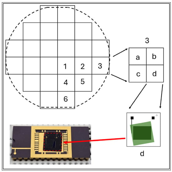
Figure 1.
Illustration of a 100 mm silicon wafer featuring an array of 24 squares, alongside a detailed view of square number 3, which measures 16.6 mm on each side. Each square contains four identical solar cell patterns. A detailed view of cell ‘d’ with a graphene membrane is shown. The final solar cell is wire-bonded into a 28-pin package as shown.
3. Results and Discussion
3.1. Removing Thermal Oxide
Once the wafer was diced into 24 nearly identical chips, the next step was to prepare a chip for oxide removal. The oxide removal pattern is shown in solid black throughout Figure 2a. The dotted or broken lines are not for oxide removal but are shown to illustrate the locations of the four 8.3 mm square solar cells and to aid in communicating the processing steps. Each device contains a 4 mm by 3 mm rectangle near the center, which later becomes the photovoltaic region. Each chip has a 500 μm by 500 μm square box at one corner, which later becomes a silicon bonding pad. Each chip has a crosshair in one corner to enable alignment to future layers. Also, at the bottom of the entire chip is a triangle shape used to help with overall chip orientation throughout the processing steps.
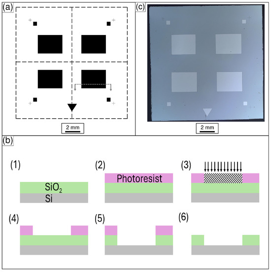
Figure 2.
Oxide removal process. (a) The pattern to be etched is shown in solid black, while the dashed lines show the four solar cells. (b) Six processing steps are shown in cross-section for the location marked in (a): (1) clean and anneal wafer; (2) add photoresist and anneal; (3) pattern the chip using maskless photolithography; (4) develop the exposed photoresist; (5) remove the oxide using 5:1 buffered oxide etch; (6) remove the unexposed photoresist. (c) Optical image after oxide removal.
A diagram showing the different steps for oxide removal is shown in Figure 2b. The cross-sectional views shown are for the region marked by the dashed line with arrows in Figure 2a. First, the chip is placed in isopropyl alcohol (IPA) at room temperature inside an ultrasonic cleaner for 10 min to produce a dust-free chip as shown in step (1). After drying with nitrogen, it is annealed at 200 °C for 15 min to remove any remaining moisture. Next, a layer of photoresist is spin-coated at 3000 rpm for 1 min on top of the oxide and annealed at 110 °C for 3 min to produce the stack shown in step (2). A maskless photolithography process is then used to transfer the pattern shown in Figure 2a onto the chip as illustrated in step (3). Next, the chip is immersed in a developer solution for 30 s followed by deionized water for 1 min to remove the exposed photoresist as shown in step (4). The chip is then immersed in a 5:1 buffered oxide etch solution for 25 min to expose the bare silicon underneath as illustrated in step (5). After the etching process, the chip is double-rinsed in deionized water for at least 10 min. Finally, any unexposed photoresist is removed by placing the chip in a stripper solution held at 80 °C for 60 min as shown in step (6). The chip is sequentially ultrasonically cleaned in acetone and then IPA. An optical microscope image of the chip after oxide removal is shown in Figure 2c. One can easily see the four large regions for graphene transfer, the four bonding pads, the four cross-hairs, and the triangle.
3.2. Adding Metal Contacts
Once the oxide has been removed, the next step is to add metal contacts. The pattern used for metal exposure is shown as solid black regions in Figure 3a. Again, the dashed lines are only there to aid the sample and process description. Notice that each solar cell has two square bonding pads that measure 500 μm by 500 μm. The upper left bonding pad is positioned precisely over the previously etched region that now has bare silicon. The other bonding pad has a rectangular stem that is 1000 μm long by 100 μm wide. The stem touches the bonding pad and is used for contacting the graphene as discussed later. The bonding pad and rectangular stem are drawn on the oxide surface so they are electrically isolated from the silicon substrate.
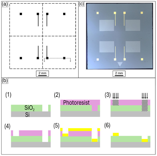
Figure 3.
Metal deposition process. (a) Pattern for metal deposition is shown in solid black, while the dashed lines show the four solar cells. (b) Six processing steps are shown in cross-section for the location marked in (a): (1) clean and anneal wafer; (2) add photoresist and anneal; (3) pattern the chip using maskless photolithography; (4) develop the exposed photoresist; (5) deposit metal; (6) remove the unexposed photoresist. (c) Optical image after metal deposition.
The metallization processing steps are illustrated in Figure 3b. An etched chip in cross-section is shown in (1). Notice that the dashed line in Figure 3a marks the cross-sectional view and shows that the left contact pad is on the oxide and the right contact pad is on the bare silicon. A photoresist layer is spin-coated onto the chip and annealed like earlier as shown in (2). A maskless photolithography process is used to transfer the pattern shown in Figure 3a onto the chip as illustrated in step (3). Next, the chip is immersed in a developer solution for 30 s followed by deionized water for 1 min to remove the exposed photoresist as shown in step (4). Next, 2 nm of chromium followed by 100 nm of gold is deposited in step (5). Finally, any unexposed photoresist is removed by placing the chip in a stripper solution held at 80 °C for 60 min as shown in step (6). The chip is sequentially ultrasonically cleaned in acetone and then IPA. An optical microscope image of the chip after metal deposition is shown in Figure 3c. One can easily see the eight gold bonding pads and the four gold stems. Notice that the stems run adjacent to the bare silicon region but do not touch it.
3.3. Overlay Multilayer Graphene
Once metal has been deposited, the next step is to overlay graphene. The chip is first cleaved along the two central dotted lines shown in Figure 3a to produce four individual solar cells. After ultrasonic cleaning in IPA, the solar cell is ready for graphene transfer. An ideal illustration of graphene placement on the solar cell is shown in Figure 4a. Notice that the graphene covers the large bare silicon region and rests on the rectangular metal stem but avoids touching either bonding pad. Commercially available multilayer graphene is used. The graphene, as purchased, is sandwiched between a sheet of polymer and a layer of polymethyl methacrylate (PMMA).
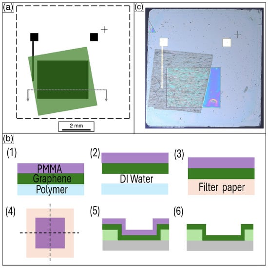
Figure 4.
Overlaying multilayer graphene process. (a) Illustration of the ideal placement of graphene on the chip covering the bare silicon and the metal stem. (b) Six processing steps are shown in the cross-section for the location marked in (a): (1) commercially available 10 mm by 10 mm PMMA–graphene–polymer stack; (2) PMMA–graphene separates from the polymer as it is placed in DI water; (3) PMMA–graphene is scooped out of the water on filter paper; (4) the PMMA–graphene–paper stack is cut into four equal sizes and placed back into the water; (5) the PMMA–graphene stack is scooped out of the DI water onto the chip and dried; (6) the PMMA is removed from the graphene using acetone if desired. (c) Optical image showing PMMA–graphene stack on chip. Solar chip functions with the PMMA left as a transparent protective coating.
The graphene transfer processing steps are illustrated in Figure 4b. The starting graphene material measures 10 mm by 10 mm and is shown in the cross-section in step (1). Submerging the starting material into deionized (DI) water at an angle separates the polymer from the graphene–PMMA stack as illustrated in step (2). Next, the PMMA-coated graphene is scooped out of the DI water on filter paper as shown in step (3). We cut the PMMA–graphene–paper stack with scissors into four equally sized pieces as shown in step (4). Submerging the individual pieces in DI water releases the PMMA–graphene from the filter paper. Next, the PMMA-coated graphene is scooped out of the DI water onto the chip as illustrated in step (5). If the graphene is not in the correct location when the chip is pulled out of the water, the chip can be resubmerged to try again. If the graphene is slightly out of position or too wrinkled, it can be gently slid with tweezers when wet. Sometimes, a large water drop lies under the graphene, and it is important to drain this using filter paper before tilting the chip. Once the graphene is in the correct position and flat, tilt the chip at a 45° angle for 15 to 20 min to drain and dry. Afterward, anneal the chip at 110 °C for 20 min. After cooling, spin-coat another layer of PMMA at 3000 rpm for 1 min onto the chip and let it cure at room temperature. This will improve the graphene–silicon contact by allowing the graphene to relax, as reported by Li et al. [35]. The PMMA can be left as a transparent coating or dissolved in acetone after 15 min and rinsed with IPA as shown in step (6). An optical image of the sample after PMMA–graphene transfer is shown in Figure 4c. Notice that the graphene mostly covers the bare silicon (graphene area = 9 mm2), and mostly covers the metal stem, but does not touch either bonding pad.
3.4. Solar Cell Performance
Once the graphene has been transferred to the chip, the solar cell is complete. For ease of handling, we next mount the chip into a standard breadboard 28-pin package as shown in Figure 5a. The chip is wire-bonded to the package, and then through the use of a breadboard, it is wired to the test circuit as shown in Figure 5b. The circuit has a DC power supply and an ammeter. With the use of a 100 W white light source (LED, 400–700 nm wavelength, 1400 W/m2), the current vs. voltage results are shown in Figure 5c (note that the dark current grows linearly from 0 to 3 μA at 0.4 V). When the bias voltage is 0, 160 μA of current flows counterclockwise through the circuit (A). As the bias voltage is increased, the current is reduced to 0 around 420 mV ( V, fill factor , efficiency ). After six months, the current–voltage characteristics remain unchanged. An idealized energy band diagram of the graphene–silicon Schottky junction is shown in Figure 5d. In this diagram, eV is the work function of graphene, and eV is the electron affinity of the silicon [36]. For simplicity, we show the Fermi level, , at the conduction band minimum, . The silicon bands bend up to meet the graphene, and this forms the Schottky barrier. When light strikes the silicon, its electrons are promoted from the valance band, to the conduction band. The hole current flows through the graphene and then counterclockwise around the circuit to the silicon.
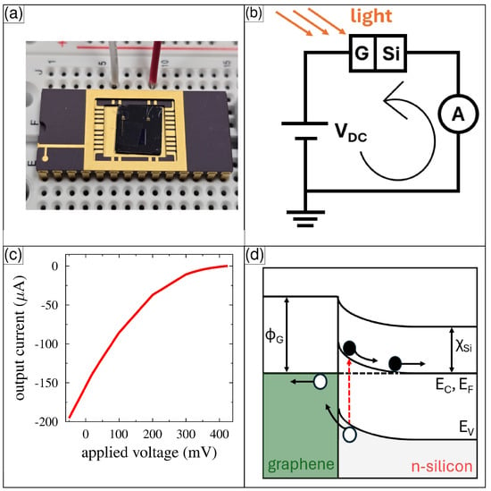
Figure 5.
Single solar cell performance. (a) Optical photograph showing a solar cell with PMMA in the package. (b) Electrical schematic used for measurement. (c) Current vs. voltage data set for the solar cell shown in (a). (d) Schottky band diagram with electrons and holes.
3.5. Solar Cell Power System
Our power system consists of a 3-volt rechargeable battery connected to a series of individual solar cells as shown in the photograph in Figure 6a. To characterize the series of solar cells, we first connect it to our power supply–ammeter circuit shown in Figure 5b. With the 100 W light source, we obtained the current–voltage data set shown in Figure 6b. This plot is similar to the one shown in Figure 5c for a single solar cell, except the short-circuit current is now 50 μA and the open-circuit voltage is now 3.3 V. This is enough voltage to recharge the 3-volt battery. A schematic of our 3-volt power system is shown in Figure 6c. Any 3-volt application, like a sensor, is connected across the 3-volt rechargeable battery. The battery continuously powers the application. When light shines on the solar cells, current will flow to recharge the battery without disrupting the application. We recharged a dead battery to provide an example as shown in Figure 6d. The battery voltage (left axes) in time is shown in red, and the current flowing into the battery (right axes) in time is shown in blue. During this time, the voltage increases from 1 to 2.6 V, while the charging current drops from 25 μA to 5 μA.
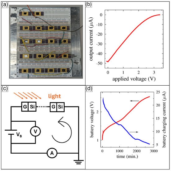
Figure 6.
Solar cell power system performance. (a) Photograph of multiple solar cells and a 3-volt rechargeable battery. (b) Current vs. voltage performance of the multiple solar cells connected together in series. (c) Circuit diagram for solar cell battery power system. (d) Battery voltage and current as a function of time during recharging.
Through connecting a device in parallel with the battery and the series of solar cells, the power system can operate whether the solar cells are illuminated or not. The battery used here has a maximum capacity of 2 mAh or a total charge of 7.2 C. Ultra-low power sensors today can run with just 16 nanoamps of current, providing a lifetime of over 17,000 h. Using a low-power device with an ultra-low duty cycle can reduce the current drawn substantially, thereby allowing intermittent solar cell recharging to maintain a long life. Therefore, the system only requires 50 h of solar charging within 17,000 h of use.
4. Summary
In this study, we fabricated a 3-volt power system for low-power-consuming applications. Starting with a 100 mm diameter silicon wafer, coated with a wet thermal oxide layer, we can make 96 solar cells. After dicing the wafer, we pattern the chips for select area oxide removal. Next, a metal is deposited to create two bonding pads and a rectangular stem to contact the graphene. Multilayer graphene is transferred onto the exposed silicon to create the photovoltaic region. The solar cells are placed in a 28-pin package and tested. Our best cell provides a short-circuit current of 160 μA and an open-circuit voltage of 420 mV. After connecting many solar cells in series, they provide a short-circuit current of 50 μA and an open-circuit voltage of 3.3 V. We combine the solar cell series with a rechargeable battery to create a 3-volt power system.
Author Contributions
Conceptualization, P.M.T.; methodology, S.M.R., M.R.K., T.B.A. and P.M.T.; software, S.M.R., J.M.M. and T.B.A.; validation, J.M.M., A. and P.M.T.; formal analysis, S.M.R. and P.M.T.; resources, P.M.T.; data curation, S.M.R., J.M.M. and T.B.A.; writing—original draft preparation, S.M.R. and P.M.T.; writing—review and editing, all authors; supervision, P.M.T.; project administration, P.M.T.; funding acquisition, P.M.T. All authors have read and agreed to the published version of the manuscript.
Funding
This research was funded by WoodNext Foundation, grant number AWD-104384.
Data Availability Statement
The data that support the findings in this study are available from the corresponding author upon reasonable request.
Acknowledgments
This work was financially supported, in part, by a grant from the WoodNext Foundation, which is administered by the Greater Houston Community Foundation.
Conflicts of Interest
The authors declare no conflicts of interest. The funders had no role in the design of the study; in the collection, analyses, or interpretation of data; in the writing of the manuscript; or in the decision to publish the results.
References
- Hanson, S.; Seok, M.; Lin, Y.-S.; Foo, Z.; Kim, D.; Lee, Y.; Liu, N.; Sylvester, D.; Blaauw, D. A low-voltage processor for sensing applications with picowatt standby mode. IEEE J. Solid-State Circuits 2009, 44, 1145–1155. [Google Scholar] [CrossRef]
- Roundy, S.; Wright, P.K.; Rabaey, J. A study of low level vibrations as a power source for wireless sensor nodes. Comput. Commun. 2003, 26, 1131–1144. [Google Scholar] [CrossRef]
- Wang, L.; Yuan, F.G. Energy harvesting by magnetostrictive material (MsM) for powering wireless sensors in SHM. Sens. Smart Struct. 2007, 6529, 1231–1241. [Google Scholar]
- Lopez-Suarez, M.; Rurali, R.; Gammaitoni, L.; Abadal, G. Nanostructured graphene for energy harvesting. Phys. Rev. B 2011, 84, 161401. [Google Scholar] [CrossRef]
- Wang, Z.L.; Wu, W. Nanotechnology-enabled energy harvesting for self-powered micro-/nanosystems. Angew. Chem. Int. Ed. 2012, 51, 11700–11721. [Google Scholar] [CrossRef] [PubMed]
- El Mahboubi, F.; Bafleur, M.; Boitier, V.; Dilhac, J.-M. Energy-harvesting powered variable storage topology for battery-free wireless sensors. Technologies 2018, 6, 106. [Google Scholar] [CrossRef]
- Torres, E.O.; Rincón-Mora, G.A. Electrostatic energy harvester and Li-ion charger circuit for micro-scale applications. In Proceedings of the 49th IEEE International Midwest Symposium on Circuits and Systems, San Juan, PR, USA, 6–9 August 2006; pp. 65–69. [Google Scholar]
- Thibado, P.M.; Neu, J.C.; Kumar, P.; Singh, S.; Bonilla, L.L. Charging capacitors from thermal fluctuations using diodes. Phys. Rev. E 2023, 108, 024130. [Google Scholar] [CrossRef] [PubMed]
- Gikunda, M.N.; Harerimana, F.; Mangum, J.M.; Rahman, S.; Thompson, J.P.; Harris, C.T.; Churchill, H.O.H.; Thibado, P.M. Array of Graphene Variable Capacitors on 100 mm Silicon Wafers for Vibration-Based Applications. Membranes 2022, 12, 533. [Google Scholar] [CrossRef]
- Le, T.K.; Mai, T.H.; Iqbal, M.A.; Vernardou, D.; Dao, V.; Ponnusamy, V.K.; Rout, C.S.; Pham, P.V. Advances in solar energy harvesting integrated by van der Waals graphene heterojunctions. RSC Adv. 2023, 13, 31273–31291. [Google Scholar] [CrossRef] [PubMed]
- Bonaccorso, F.; Sun, Z.; Hasan, T.; Ferrari, A. Graphene photonics and optoelectronics. Nat. Photonics 2010, 4, 611–622. [Google Scholar] [CrossRef]
- Novoselov, K.; Fal’ko, V.; Colombo, L.; Gellert, P.; Schwab, M.; Kim, K. A roadmap for graphene. Nature 2012, 490, 192–200. [Google Scholar] [CrossRef] [PubMed]
- De Arco, L.G.; Zhang, Y.; Schlenker, C.W.; Ryu, K.; Thompson, M.E.; Zhou, C.W. Continuous, Highly Flexible, and Transparent Graphene Films by Chemical Vapor Deposition for Organic Photovoltaics. ACS Nano 2010, 4, 2865–2873. [Google Scholar] [CrossRef] [PubMed]
- Singh, E.; Nalwa, H.S. Graphene-Based Bulk-Heterojunction Solar Cells: A Review. J. Nanosci. Nanotechnol. 2015, 15, 6237–6278. [Google Scholar] [CrossRef] [PubMed]
- Kong, X.; Zhang, L.; Liu, B.; Gao, H.; Zhang, Y.; Yan, H.; Song, X. Graphene/Si Schottky solar cells: A review of recent advances and prospects. RSC Adv. 2019, 9, 863–877. [Google Scholar] [CrossRef] [PubMed]
- Stoller, M.; Park, S.; Zhu, Y.; An, J.; Ruoff, R. Graphene-Based Ultracapacitors. Nano Lett. 2008, 8, 3498–3502. [Google Scholar] [CrossRef]
- Hsieh, Y.P.; Hong, B.J.; Ting, C.C.; Hofmann, M. Ultrathin graphene-based solar cells. RSC Adv. 2015, 5, 99627–99631. [Google Scholar] [CrossRef]
- Li, X.M.; Lv, Z.; Zhu, H.W. Carbon/Silicon Heterojunction Solar Cells: State of the Art and Prospects. Adv. Mater. 2015, 27, 6549–6574. [Google Scholar] [CrossRef]
- Mahmoudi, T.; Wang, Y.; Hahn, Y.-B. Graphene and its derivatives for solar cells application. Nano Energy 2018, 47, 51. [Google Scholar] [CrossRef]
- Lancellotti, L.; Lisi, N.; Veneri, P.D.; Bobeico, E.; Matacena, I.; Guerriero, P. Graphene-on-Silicon solar cells with graphite contacts. In Proceedings of the 2019 International Conference on Clean Electrical Power (ICCEP), Otranto, Italy, 2–4 July 2019; pp. 199–203. [Google Scholar]
- Matacena, I.; Lancellotti, L.; Lisi, N.; Delli Veneri, P.; Guerriero, P.; Daliento, S. Impedance Spectroscopy for the Characterization of the All-Carbon Graphene-Based Solar Cell. Energies 2020, 13, 1908. [Google Scholar] [CrossRef]
- Rehman, M.A.; Roy, S.B.; Akhtar, I.; Bhopal, M.F.; Choi, W.; Nazir, G.; Khan, M.F.; Kumar, S.; Eom, J.; Chun, S.H.; et al. Thickness-dependent efficiency of directly grown graphene based solar cells. Carbon 2019, 148, 187–195. [Google Scholar] [CrossRef]
- Choi, Y.; Lee, J.; Seo, J.; Jung, S.; Kim, U.; Park, H. The effect of the graphene integration process on the performance of graphene-based Schottky junction solar cells. J. Mater. Chem. A 2017, 5, 18716–18724. [Google Scholar] [CrossRef]
- Ju, S.H.; Liang, B.X.; Wang, J.Z.; Shi, Y.; Li, S.L. Graphene/silicon Schottky solar cells: Technical strategies for performance optimization. Opt. Commun. 2018, 428, 258–268. [Google Scholar] [CrossRef]
- Gnisci, A.; Faggio, G.; Lancellotti, L.; Messina, G.; Carotenuto, R.; Bobeico, E.; Delli Veneri, P.; Capasso, A.; Dikonimos, T.; Lisi, N. The Role of Graphene-Based Derivative as Interfacial Layer in Graphene/n-Si Schottky Barrier Solar Cells. Phys. Status Solidi A Appl. Mater. Sci. 2019, 216, 1900351. [Google Scholar] [CrossRef]
- Jehad, A.K.; Yurddaskal, M.; Gunes, F.; Zafer, C.; Kocabas, K. Investigation of graphene-based Schottky junction solar cell with heavy-doped silicon. J. Mater. Sci. Mater. Electron. 2021, 32, 28856–28869. [Google Scholar] [CrossRef]
- Cui, T.; Lv, R.; Huang, Z.-H.; Chen, S.; Zhang, Z.; Gan, X.; Jia, Y.; Li, X.; Wang, K.; Wua, D.; et al. Enhanced efficiency of graphene/silicon heterojunction solar cells by molecular doping. J. Mater. Chem. A 2013, 1, 5736. [Google Scholar] [CrossRef]
- Matacena, I.; Guerriero, P.; Lancellotti, L.; Bobeico, E.; Lisi, N.; Chierchia, R.; Veneri, P.; Daliento, S. Capacitance–Voltage Investigation of Encapsulated Graphene/Silicon Solar Cells. IEEE Trans. Electron Devices 2023, 70, 4243. [Google Scholar] [CrossRef]
- Fallahazad, P.; Naderi, N.; Eshraghi, M.J. Improved photovoltaic performance of graphene-based solar cells on textured silicon substrate. J. Alloys Compd. 2020, 834, 152514. [Google Scholar] [CrossRef]
- Arefinia, Z.; Asgari, A. A new modeling approach for graphene-based silicon nanowire Schottky junction solar cells. J. Renew. Sustain. Energy 2014, 6, 043102. [Google Scholar] [CrossRef]
- Li, X.M.; Zhu, H.W.; Wang, K.L.; Cao, A.Y.; Wei, J.Q.; Li, C.Y.; Jia, Y.; Li, Z.; Li, X.; Wu, D.H. Graphene-On-Silicon Schottky Junction Solar Cells. Adv. Mater. 2010, 22, 2743–2748. [Google Scholar] [CrossRef]
- Ye, Y.; Dai, L. Graphene-based Schottky junction solar cells. J. Mater. Chem. 2012, 22, 24224–24229. [Google Scholar] [CrossRef]
- Li, Y.F.; Yang, W.; Tu, Z.Q.; Liu, Z.C.; Yang, F.; Zhang, L.Q.; Hatakeyama, R. Schottky junction solar cells based on graphene with different numbers of layers. Appl. Phys. Lett. 2014, 104, 113902. [Google Scholar] [CrossRef]
- Song, Y.; Li, X.; Mackin, C.; Zhang, X.; Fang, W.; Palacios, T.; Zhu, H.; Kong, J. Role of Interfacial Oxide in High-Efficiency Graphene-Silicon Schottky Barrier Solar Cells. Nano Lett. 2015, 15, 2104–2110. [Google Scholar] [CrossRef] [PubMed]
- Li, X.; Zhu, Y.; Cai, W.; Borysiak, M.; Han, B.; Chen, D.; Piner, R.; Colombo, L.; Ruoff, R. Transfer of Large-Area Graphene Films for High-Performance Transparent Conductive Electrodes. Nano Lett. 2009, 9, 4359–4363. [Google Scholar] [CrossRef] [PubMed]
- Das, S.; Sudhagar, P.; Kang, Y.S.; Choi, W. Graphene synthesis and application for solar cells. J. Mater. Res. 2014, 29, 299–319. [Google Scholar] [CrossRef]
Disclaimer/Publisher’s Note: The statements, opinions and data contained in all publications are solely those of the individual author(s) and contributor(s) and not of MDPI and/or the editor(s). MDPI and/or the editor(s) disclaim responsibility for any injury to people or property resulting from any ideas, methods, instructions or products referred to in the content. |
© 2024 by the authors. Licensee MDPI, Basel, Switzerland. This article is an open access article distributed under the terms and conditions of the Creative Commons Attribution (CC BY) license (https://creativecommons.org/licenses/by/4.0/).