
High-Performance Wireless Power and Data Transmission System for Medical Implant Devices Using ASK Modulation

Abstract
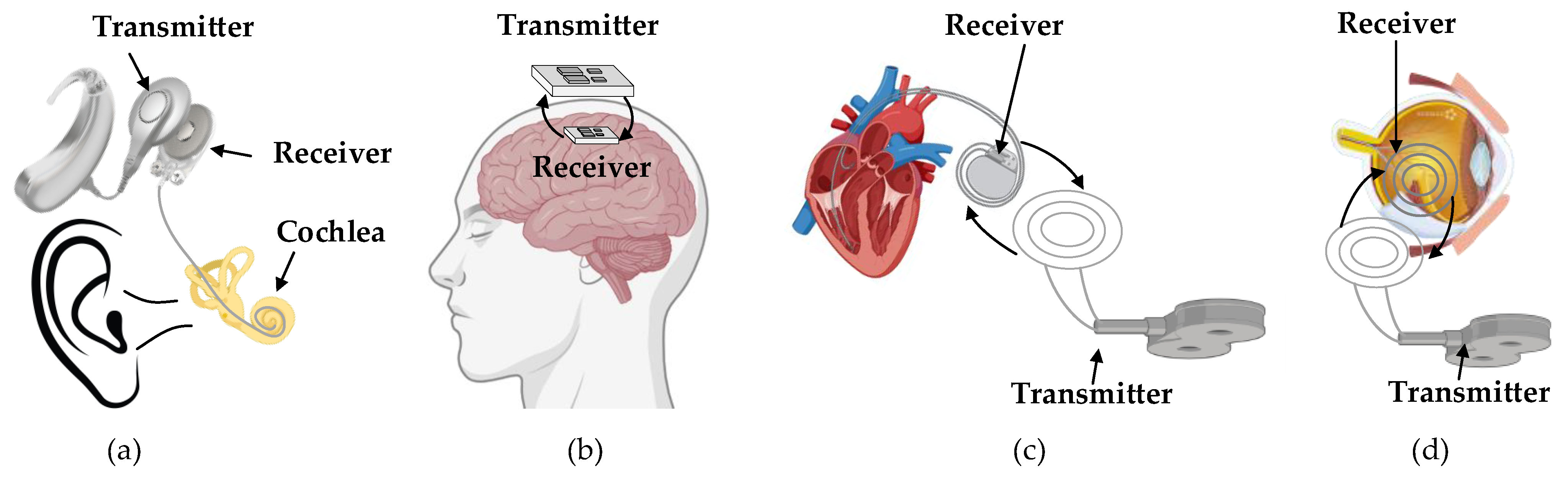
:1. Introduction
2. Efficiency Analysis and Derivation of Wireless Power Transmission
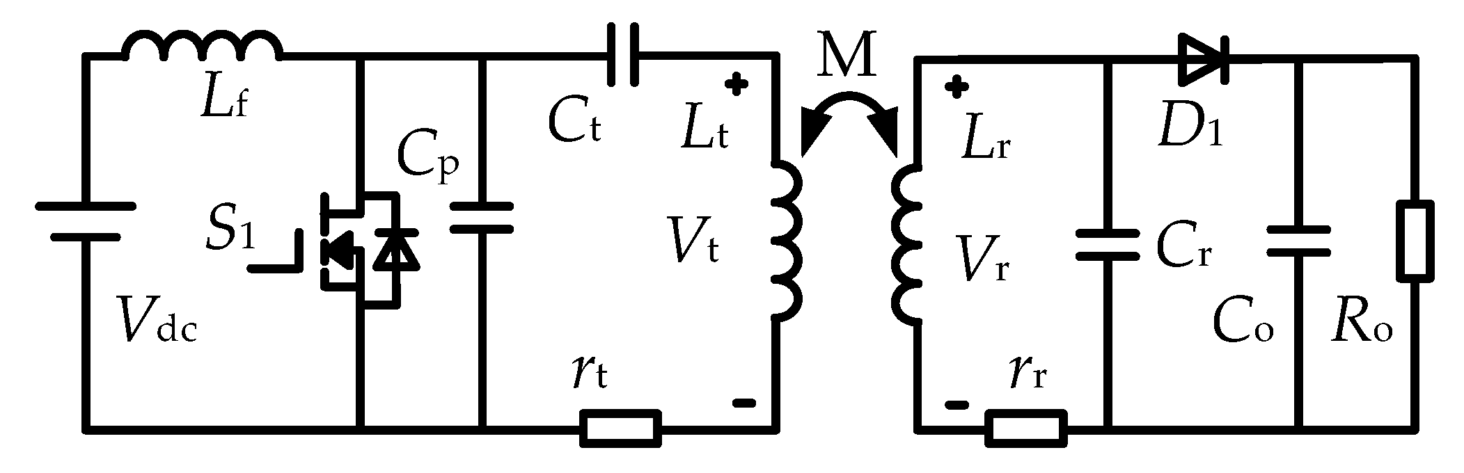
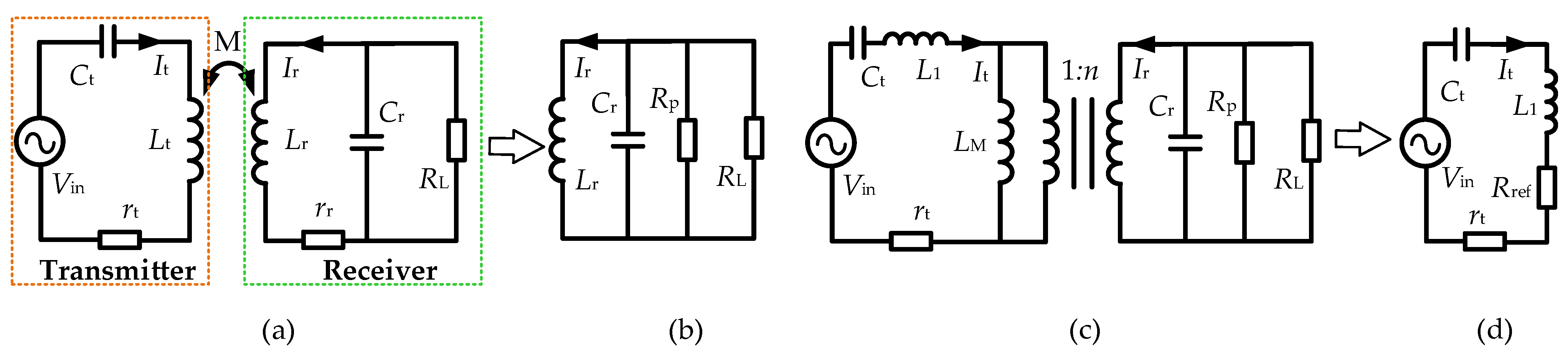
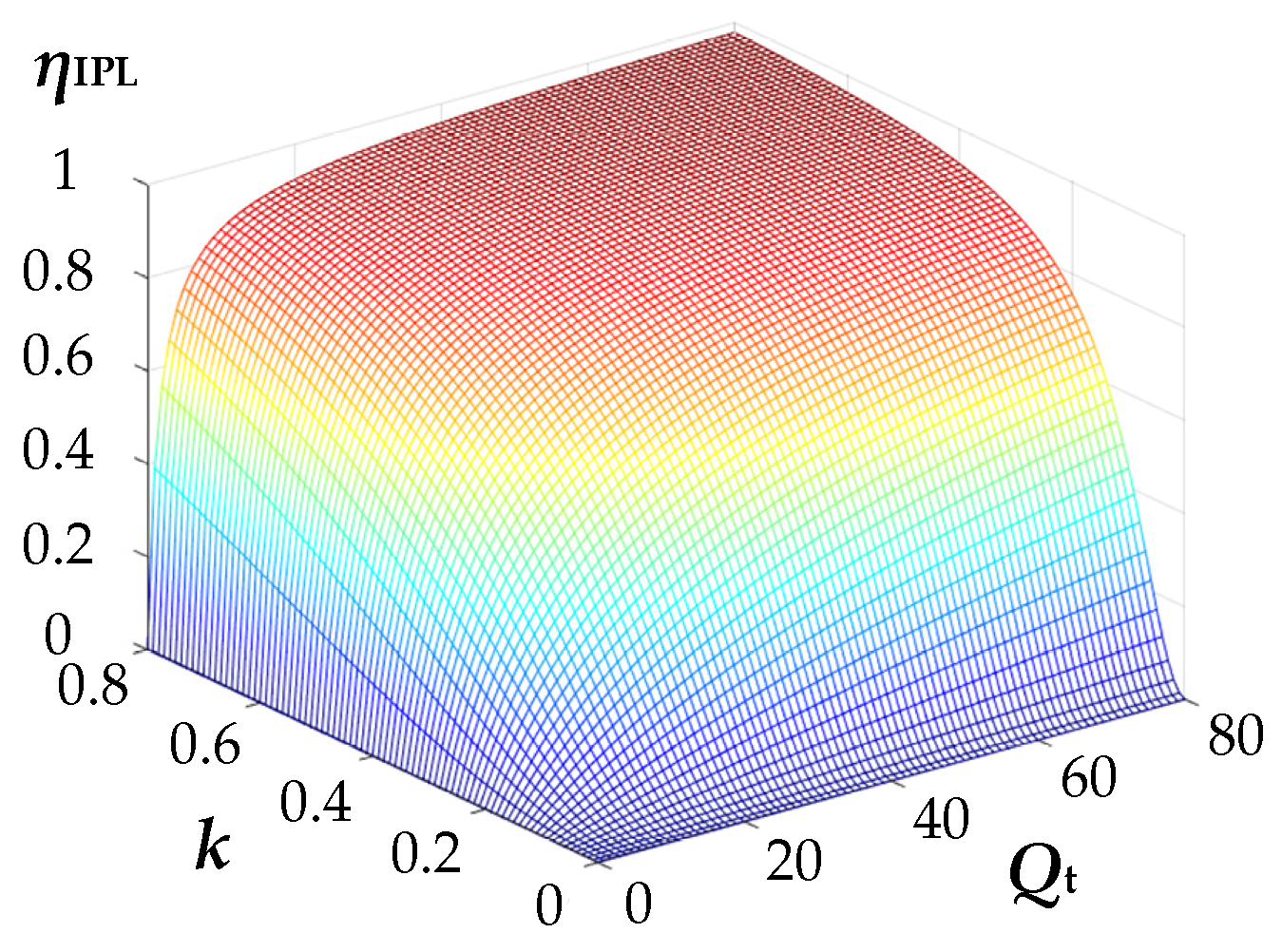
2.1. Inductive Power Transmission Link Characteristic Analysis
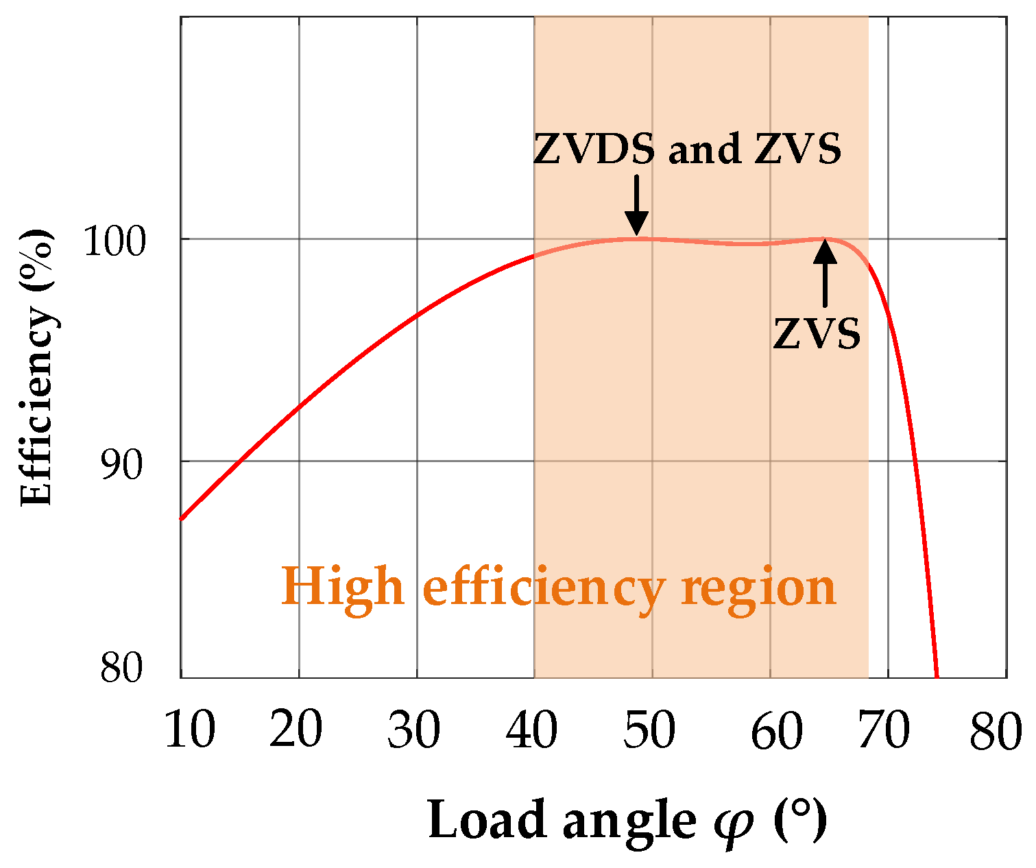
2.2. Class-E Power Amplifier Characteristic Analysis
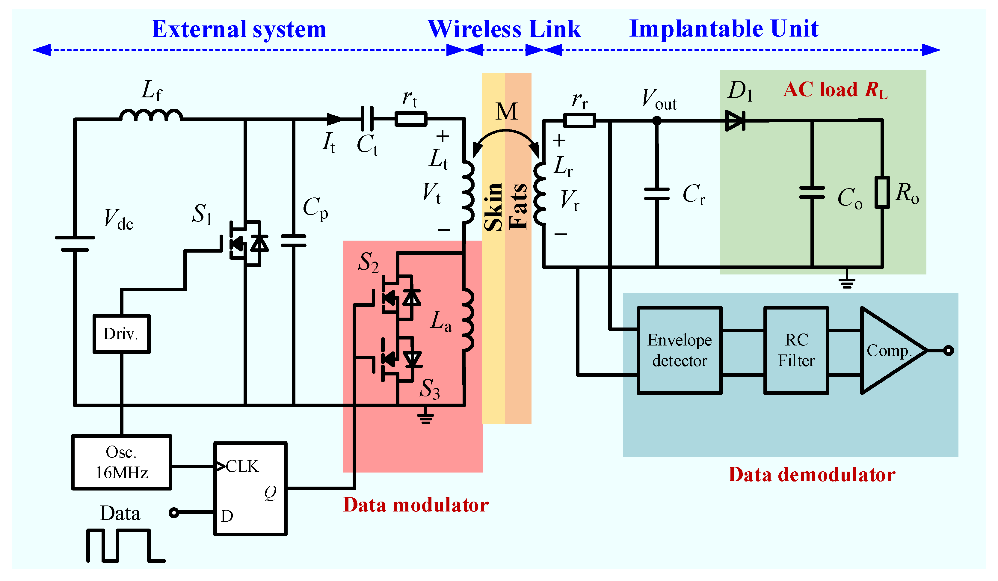
3. Proposed Circuit with ASK Modulation
3.1. Operation Principle
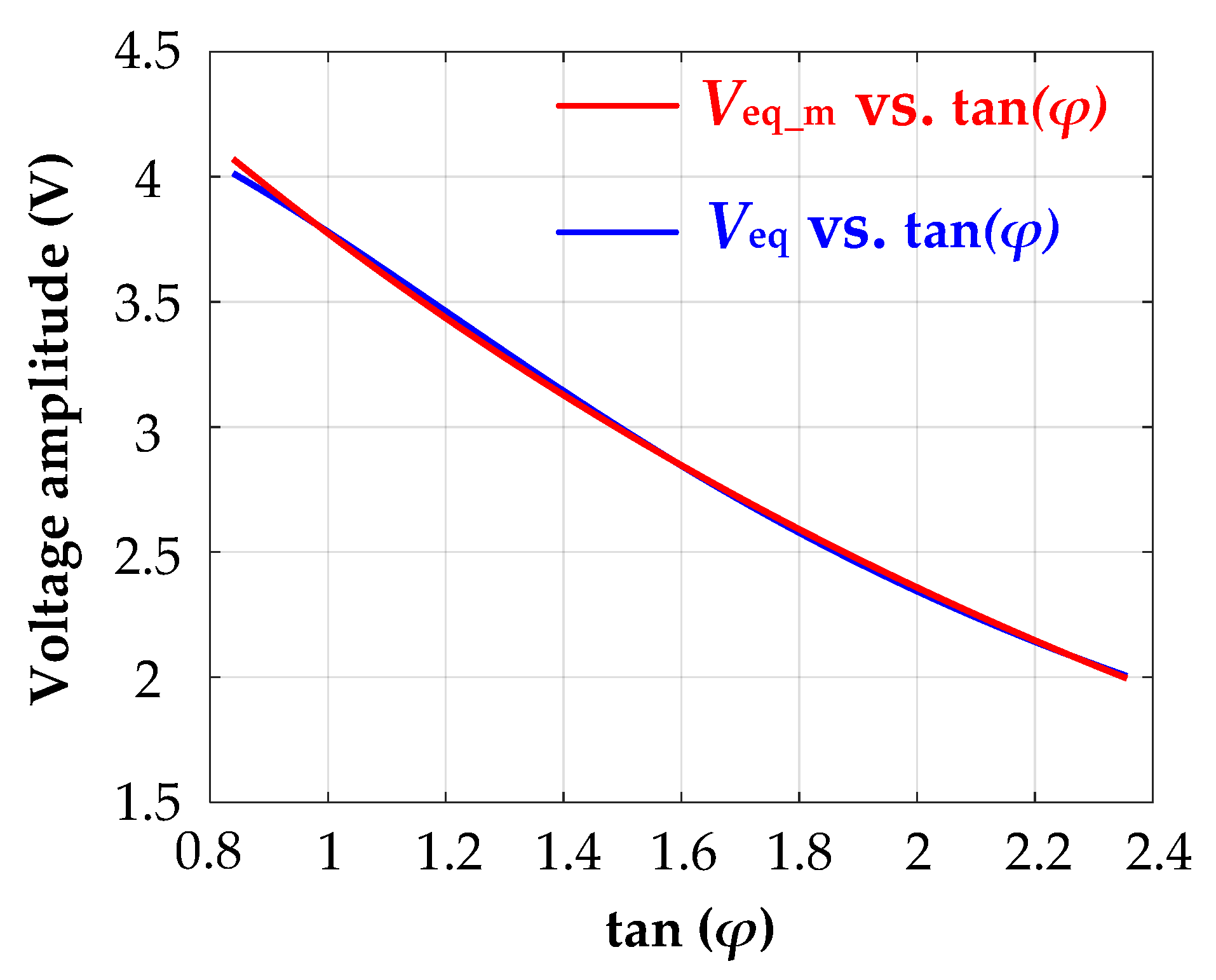
3.2. Relationship between Vout and φ
3.3. La Calculation
3.4. Design Procedure
4. Simulation and Experimental Results
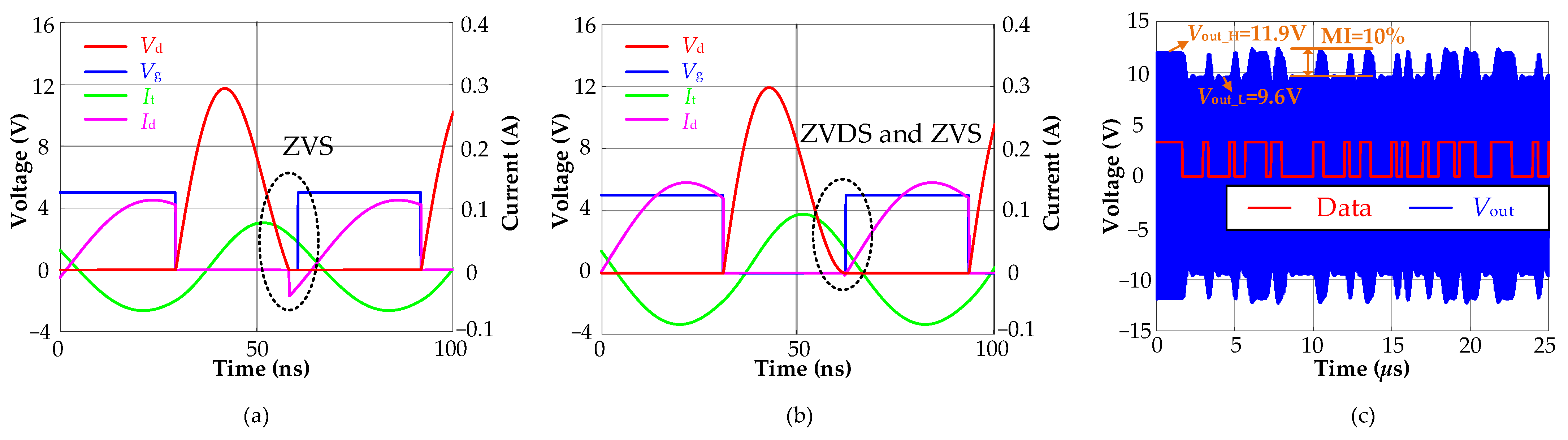
4.1. Simulation Results
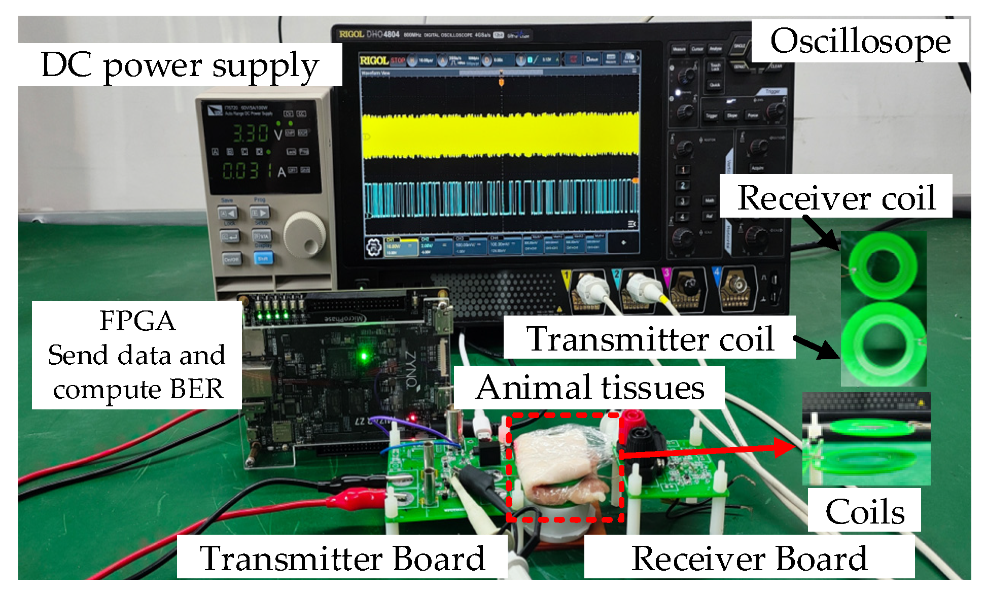
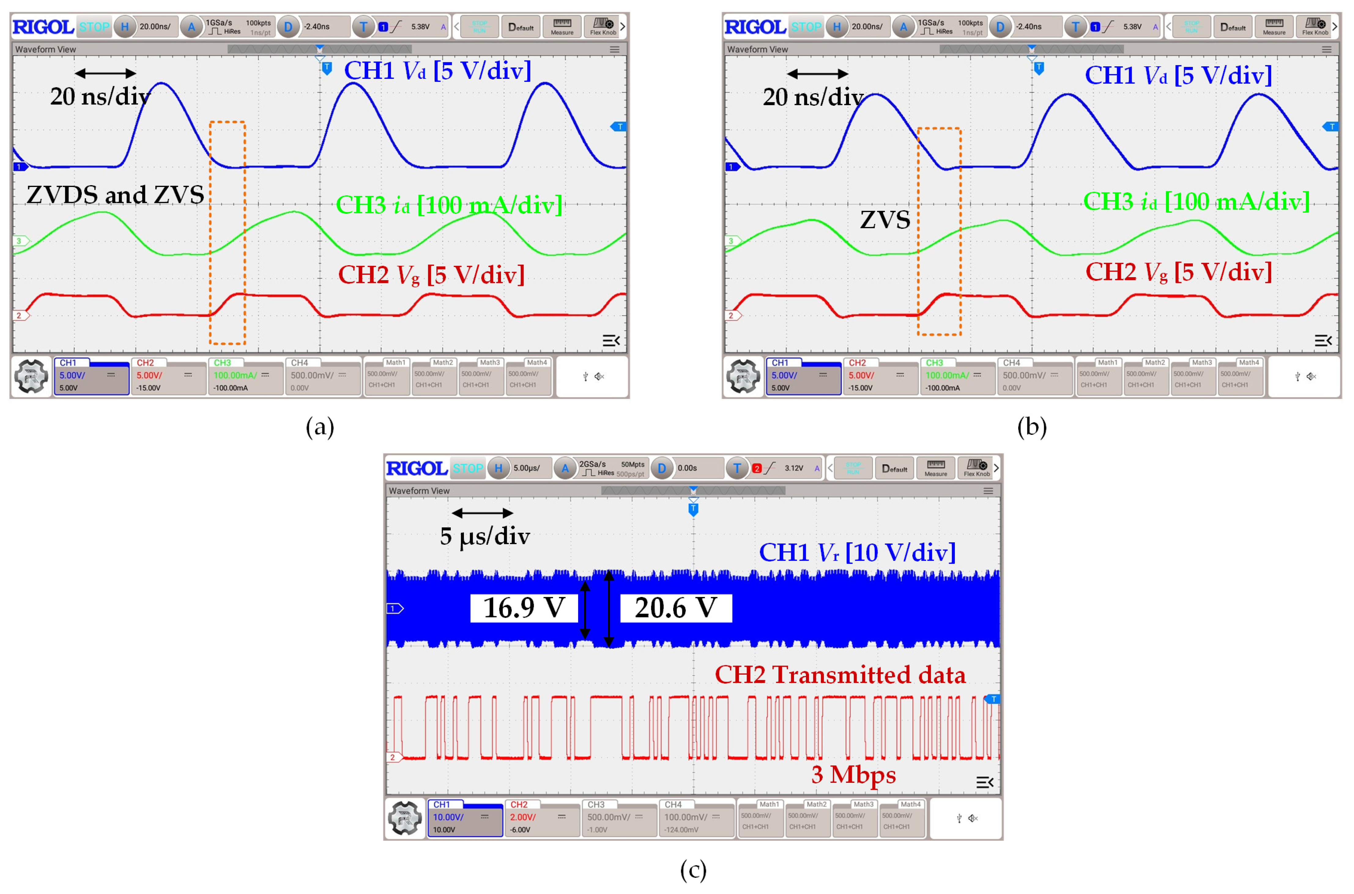
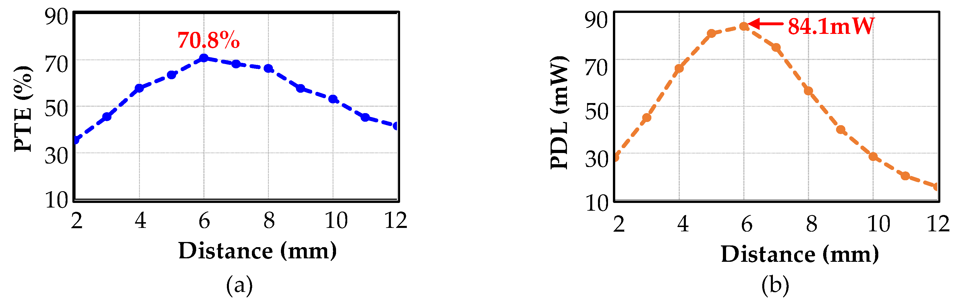
4.2. Experimental Results
5. Conclusions
Author Contributions
Funding
Data Availability Statement
Conflicts of Interest
References
- Henry, F.; Glavin, M.; Jones, E. Noise Reduction in Cochlear Implant Signal Processing: A Review and Recent Developments. IEEE Rev. Biomed. Eng. 2023, 16, 319–331. [Google Scholar] [CrossRef] [PubMed]
- Rezaeiyan, Y.; Zamani, M.; Shoaei, O.; Serdijn, W.A. Mixed-signal IC with pulse width modulation wireless telemetry for implantable cardiac pacemakers in 0.18-μm CMOS. IEEE Trans. Biomed. Circuits Syst. 2018, 12, 589–600. [Google Scholar] [CrossRef] [PubMed]
- Kim, J.; Park, S.; Oh, S.; Huh, Y.; Cho, J.; Oh, J. Cage-Embedded Crown-Type Dual Coil Wireless Power Transfer Based Microwave Brain Stimulation System for Untethered and Moving Mice. IEEE Trans. Biomed. Circuits Syst. 2023, 17, 362–374. [Google Scholar] [CrossRef] [PubMed]
- Park, Y.; Koh, S.T.; Lee, J.; Kim, H.; Choi, J.; Ha, S.; Kim, C.; Je, M. A Wireless Power and Data Transfer IC for Neural Prostheses Using a Single Inductive Link with Frequency-Splitting Characteristic. IEEE Trans. Biomed. Circuits Syst. 2021, 15, 1306–1319. [Google Scholar] [CrossRef] [PubMed]
- Trigui, A.; Hached, S.; Ammari, A.C.; Savaria, Y.; Sawan, M. Maximizing data transmission rate for implantable devices over a single inductive link: Methodological review. IEEE Rev. Biomed. Eng. 2018, 12, 72–87. [Google Scholar] [CrossRef]
- Lee, E.K.F. A discrete controlled fully integrated class E coil driver with power efficient ASK modulation for powering biomedical implants. IEEE Trans. Circuits Syst. I Reg. Papers 2015, 62, 1678–1687. [Google Scholar] [CrossRef]
- Dehghan, K.; Shoaei, O.; Ashtiani, S.J. A Class-E Power and Data Transmitter with Improved Data Rate to Carrier Frequency Ratio for Medical Implants. IEEE Trans. Circuits Syst. II Exp. Briefs 2022, 69, 2692–2696. [Google Scholar] [CrossRef]
- Trigui, A.; Ali, M.; Ammari, A.C.; Savaria, Y.; Sawan, M. A 1.5-pJ/bit, 9.04-Mbit/s Carrier-Width Demodulator for Data Transmission Over an Inductive Link Supporting Power and Data Transfer. IEEE Trans. Circuits Syst. II Exp. Briefs 2018, 65, 1420–1424. [Google Scholar] [CrossRef]
- Kiani, M.; Ghovanloo, M. A 13.56-Mbps Pulse Delay Modulation Based Transceiver for Simultaneous Near-Field Data and Power Transmission. IEEE Trans. Biomed. Circuits Syst. 2015, 9, 1–11. [Google Scholar] [CrossRef] [PubMed]
- Roy, S.; Azad, A.W.; Baidya, S.; Alam, M.K.; Khan, F. Powering Solutions for Biomedical Sensors and Implants Inside the Human Body: A Comprehensive Review on Energy Harvesting Units, Energy Storage, and Wireless Power Transfer Techniques. IEEE Trans. Power Electron. 2022, 37, 12237–12263. [Google Scholar] [CrossRef]
- Huang, W.; Zheng, K.S.; Liu, X.; Wang, X.; Hou, Y.; Liu, Y. Simultaneous High-Efficiency Power Delivery and Energy-Efficient Forward Data Transmission over Single Inductive Link. IEEE Access 2023, 11, 76793–76803. [Google Scholar] [CrossRef]
- Kennedy, H.; Bodnar, R.; Lee, T.; Redman-White, W. A high-Q resonant inductive link transmit driver with adaptive-predictive phase continuous tuning and deviation frequency calibration for enhanced FSK/PSK modulation and power transfer. IEEE J. Solid-State Circuits 2020, 55, 2401–2413. [Google Scholar] [CrossRef]
- Avilés, J.P.O.; Tofoli, F.L.; Ribeiro, E.R. Novel Control Approach for Resonant Class-DE Inverters Applied in Wireless Power Transfer Systems. Energies 2023, 16, 7238. [Google Scholar] [CrossRef]
- Fu, M.; Yin, H.; Liu, M.; Ma, C. Loading and Power Control for a High-Efficiency Class E PA-Driven Megahertz WPT System. IEEE Trans. Power Electron. 2016, 63, 6867–6876. [Google Scholar] [CrossRef]
- Corti, F.; Reatti, A.; Wu, Y.-H.; Czarkowski, D.; Musumeci, S. Zero Voltage Switching Condition in Class-E Inverter for Capacitive Wireless Power Transfer Applications. Energies 2021, 14, 911. [Google Scholar] [CrossRef]
- Lee, B.; Kiani, M.; Ghovanloo, M. A triple-loop inductive power transmission system for biomedical applications. IEEE Trans. Biomed. Circuits Syst. 2016, 10, 138–148. [Google Scholar] [CrossRef] [PubMed]
- Lee, B.; Ghovanloo, M. An overview of data telemetry in inductively powered implantable biomedical devices. IEEE Commun. Mag. 2019, 57, 74–80. [Google Scholar] [CrossRef]
- Najjarzadegan, M.; Hafshejani, E.H.; Mirabbasi, S. An open-loop double-carrier simultaneous wireless power and data transfer system. IEEE Trans. Circuits Syst. II Exp. Briefs 2019, 66, 823–827. [Google Scholar] [CrossRef]
- Han, D.; Yan, G.; Jiang, P.; Wang, Z.; Wang, W. A Three-Dimensional Orthogonal Receiving Coil for In Vivo Microrobot Wireless Power Transmission Systems. Energies 2022, 15, 6321. [Google Scholar] [CrossRef]
- Yao, Y.; Sun, P.; Liu, X.; Wang, Y.; Xu, D. Simultaneous Wireless Power and Data Transfer: A Comprehensive Review. IEEE Trans. Power Electron. 2022, 37, 3650–3667. [Google Scholar] [CrossRef]
- Agarwal, K.; Jegadeesan, R.; Guo, Y.X.; Thakor, N.V. Wireless Power Transfer Strategies for Implantable Bioelectronics. IEEE Rev. Biomed. Eng. 2017, 10, 136–161. [Google Scholar] [CrossRef]
- Karimi, M.J.; Schmid, A.; Dehollain, C. Wireless Power and Data Transmission for Implanted Devices via Inductive Links: A Systematic Review. IEEE Sensors J. 2021, 21, 7145–7161. [Google Scholar] [CrossRef]
- Cheng, C.H.; Tsai, P.Y.; Yang, T.Y.; Cheng, W.H.; Yen, T.Y.; Luo, Z.; Qian, X.; Chen, Z.; Lin, T.; Chen, W.; et al. A Fully Integrated 16-Channel Closed-Loop Neural-Prosthetic CMOS SoC with Wireless Power and Bidirectional Data Telemetry for Real-Time Efficient Human Epileptic Seizure Control. IEEE J. Solid-State Circuits 2018, 53, 3314–3326. [Google Scholar] [CrossRef]
- Ahmadi, M.M.; Sarbandi-Farahani, M. A Class-E power and data transmitter with on–off keying data modulation for wireless power and data transmission to medical implants. Circuits Syst. Signal Process. 2020, 39, 4174–4186. [Google Scholar] [CrossRef]
- Ahmadi, M.M.; Ghandi, S. A Class-E Power Amplifier with Wideband FSK Modulation for Inductive Power and Data Transmission to Medical Implants. IEEE Sensors J. 2018, 18, 7242–7252. [Google Scholar] [CrossRef]
- Jiang, D.; Cirmirakis, D.; Schormans, M.; Perkins, T.A.; Donaldson, N.; Demosthenous, A. An Integrated Passive Phase-Shift Keying Modulator for Biomedical Implants with Power Telemetry over a Single Inductive Link. IEEE Trans. Biomed. Circuits Syst. 2017, 11, 64–77. [Google Scholar] [CrossRef] [PubMed]
- Chen, Y.; Liu, Y.; Li, Y.; Wang, G.; Chen, M. An Energy-Efficient ASK Demodulator Robust to Power-Carrier-Interference for Inductive Power and Data Telemetry. IEEE Trans. Biomed. Circuits Syst. 2022, 16, 108–118. [Google Scholar] [CrossRef] [PubMed]
- Navaii, M.L.; Sadjedi, H.; Sarrafzadeh, A. Efficient ASK Data and Power Transmission by the Class-E with a Switchable Tuned Network. IEEE Trans. Circuits Syst. I Reg. Papers 2018, 65, 3255–3266. [Google Scholar] [CrossRef]
- MAhmadi, M.; Pezeshkpour, S.; Kabirkhoo, Z. A High-Efficiency ASK-Modulated Class-E Power and Data Transmitter for Medical Implants. IEEE Trans. Power Electron. 2022, 37, 1090–1101. [Google Scholar] [CrossRef]
- Qu, X.; Han, H.; Wong, S.C.; Chi, K.T.; Chen, W. Hybrid IPT Topologies with Constant Current or Constant Voltage output for Battery Charging Applications. IEEE Trans. Power Electron. 2015, 30, 6329–6337. [Google Scholar] [CrossRef]
- Yousefi, A.; Abidi, A.A.; Markovic, D. Analysis and design of a robust, low-power, inductively coupled LSK data link. IEEE J. Solid-State Circuits 2020, 55, 2583–2596. [Google Scholar] [CrossRef]
- Chen, Y.; Wu, J.; Zhang, H.; Guo, L.; Lu, F.; Jin, N.; Kim, D.H. A Parameter Tuning Method for a Double-Sided Compensated IPT System with Constant-Voltage output and Efficiency Optimization. IEEE Trans. Power Electron. 2023, 38, 4124–4139. [Google Scholar] [CrossRef]
- Jegadeesan, R.; Guo, Y.X. Topology Selection and Efficiency Improvement of Inductive Power Links. IEEE Trans. Antennas Propag. 2012, 60, 4846–4854. [Google Scholar] [CrossRef]
- Beigi, A.; Tavana, F.; Haeri, A.A.R.; Safarian, A. Analysis and Design of a Duty-Cycle-Controlled Amplitude Shift Keying Class-E Power Amplifier. IEEE Trans. Power Electron. 2023, 38, 10470–10479. [Google Scholar] [CrossRef]
- Liu, M.; Fu, M.; Ma, C. Parameter Design for a 6.78-MHz Wireless Power Transfer System Based on Analytical Derivation of Class E Current-Driven Rectifier. IEEE Trans. Power Electron. 2016, 31, 4280–4291. [Google Scholar] [CrossRef]
- Raab, F. Idealized operation of the class E tuned power amplifier. IEEE Trans. Circuits Syst. 1977, 12, 725–735. [Google Scholar] [CrossRef]


| Parameters | Description | Value (Simulation/Measured) |
|---|---|---|
| fs | Carrier frequency | 16 MHz/16 MHz |
| Vdc | DC input voltage | 3.3 V/3.3 V |
| Cp | Parallel capacitor | 65 pF/60 pF |
| Ct | Series capacitor | 40 pF/43 pF |
| Lt | Transmitter coil | 3 μH/3 μH |
| Lr | Receiver coil | 1 μH/1 μH |
| La | Data modulation inductor | 0.2 μH/0.2 μH |
| k | Coupling coefficient | 0.17/0.17 |
| rt | Transmitter coil’s ESR | 0.44 Ω/0.44 Ω |
| rr | Receiver coil’ ESR | 0.36 Ω/0.36 Ω |
| RL | Load resistance | 540 Ω/540 Ω |
| Nt | Transmitter coil’s turn number | 8 |
| Nr | Receiver coil’s turn number | 5 |
Disclaimer/Publisher’s Note: The statements, opinions and data contained in all publications are solely those of the individual author(s) and contributor(s) and not of MDPI and/or the editor(s). MDPI and/or the editor(s) disclaim responsibility for any injury to people or property resulting from any ideas, methods, instructions or products referred to in the content. |
© 2024 by the authors. Licensee MDPI, Basel, Switzerland. This article is an open access article distributed under the terms and conditions of the Creative Commons Attribution (CC BY) license (https://creativecommons.org/licenses/by/4.0/).
Share and Cite
Zhu, H.; Tahir, M.; Wu, X.; Hu, S. High-Performance Wireless Power and Data Transmission System for Medical Implant Devices Using ASK Modulation. Energies 2024, 17, 731. https://doi.org/10.3390/en17030731
Zhu H, Tahir M, Wu X, Hu S. High-Performance Wireless Power and Data Transmission System for Medical Implant Devices Using ASK Modulation. Energies. 2024; 17(3):731. https://doi.org/10.3390/en17030731
Chicago/Turabian StyleZhu, Haoqi, Mustafa Tahir, Xu Wu, and Sideng Hu. 2024. "High-Performance Wireless Power and Data Transmission System for Medical Implant Devices Using ASK Modulation" Energies 17, no. 3: 731. https://doi.org/10.3390/en17030731