Article

Scaling-Up of Solution-Processable Tungsten Trioxide (WO3) Nanoparticles as a Hole Transport Layer in Inverted Organic Photovoltaics

1
CHOSE (Centre for Hybrid and Organic Solar Energy) and Department of Electronic Engineering, University Rome Tor Vergata, Via del Politecnico 1, 00133 Rome, Italy
2
DGTCSI-ISCTI (Direzione Generale per le Tecnologie delle Comunicazioni e la Sicurezza Informatica-Istituto Superiore delle Comunicazioni e delle Tecnologie Dell’informazione), Ministero dell’Impresa e del Made in Italy (MIMIt), Viale America, 201, 00144 Rome, Italy
3
Greatcell Solar Italia, Viale Castro Pretorio 122, 00185 Rome, Italy
4
SpecX-Lab, Istituto di Struttura della Materia C.N.R, Via del Fosso del Cavaliere 100, 00133 Rome, Italy
*
Author to whom correspondence should be addressed.
These authors contributed equally to this work.
Energies 2024, 17(4), 814; https://doi.org/10.3390/en17040814
Submission received: 11 January 2024 / Revised: 1 February 2024 / Accepted: 3 February 2024 / Published: 8 February 2024
(This article belongs to the Section A2: Solar Energy and Photovoltaic Systems)

Abstract

:
We reported the comparative studies of the optimization of solution-processable tungsten trioxide (WO3) as a hole transporting layer (HTL) in inverted organic photovoltaics (OPVs) using spin coating, slot-die coating, and spray coating technologies for scaling-up applications. To facilitate the technology’s transition into commercial manufacturing, it is necessary to explore the role of scalable technologies for low-cost and efficient device fabrication. We investigated the role of diluting WO3 with isopropanol as an HTL in inverted OPVs to solve the issue of poor wettability of the hydrophobic surface of the PBDB-T: ITIC bulk heterojunction layer. The optimal dilution ratios of WO3 with isopropanol were 1:4, 1:4 and 1:8 with spin coating, slot-die coating and spray coating techniques, respectively. We evaluated the device performance by conducting a current density–voltage (J-V) analysis, incident photon-to-current conversion efficiency (IPCE) measurements, and ultraviolet–visible (UV-Vis) absorbance spectra for various WO3 concentrations. The J-V characteristics revealed that slot-die coating resulted in the highest performance, followed by the spray coating technology. We further investigated the impact of the annealing temperature on device performance for both slot-die- and spray-coated diluted WO3. The highest device performance was achieved at an annealing temperature of 120 °C for both coating technologies. This research offers valuable insights into the scalable fabrication of inverted OPV devices, paving the way for cost-effective and efficient large-scale production.

1. Introduction

Photovoltaic (PV) power generation is projected to grow 6-fold, from 480 GW in 2018 to 2840 GW by 2030 [1]. According to the International Energy Agency (IEA), PV is the fastest declining cost technology among renewables, with power generation surpassing 10 trillion kWh. PV technology converts sunlight into electricity, offering a cost-effective and rapidly advancing solution to the world’s energy needs [2].
In the last few decades, emerging PV technologies such as dye-sensitized solar cells (DSSCs), perovskite solar cells (PSCs), and organic photovoltaics (OPV) [3] have been gaining interest in energy harvesting and have shown promising potential for being commercialized on a largescale [4]. These new PV technologies are considered to be the next generation of solar technology [5] and have extended the area of applications based on the first and second generation of PV technologies [3,6]. The materials used in third-generation PV are cheaper, abundant and can be processed easily using low-cost manufacturing techniques, making them more cost-effective and easily accessible to people across the globe than conventional C-Si-based PV technology [7]. Perovskite solar cells have shown remarkable efficiency, but they face challenges related to stability and the use of potentially toxic lead-based materials [8]. DSSCs, on the other hand, have a strong presence, particularly in niche applications such as low-cost, portable and disposable electronics, but their lower efficiency limits their widespread adoption [9]. Compared to perovskite and DSSC technologies, an OPV device presents distinct advantages [4]. The use of low-cost manufacturing processes makes OPVs competitive with other emerging PV and conventional energy sources in certain markets [4]. OPV technology is based on organic semiconductor materials, which have the potential for low production costs, for being lightweight, and for a large-area roll-to-roll (R2R) solution processability [10,11]. Additionally, OPVs offer stretchability/flexibility, optical tuneable transparency, and a short energy payback time (SEPBT) [11,12]. The progress in power conversion efficiency has been outstanding, as it has increased from 8% to up to 20% in just a single decade, which has increased the interest of OPVs for industrialization [13]. The highest reported value of a single-junction OPV device is around 19.2% on a laboratory scale [14]. OPVs exhibit a higher power-to-weight ratio/specific power than C-Si and thin-film solar cells [11,15,16]. This parameter is crucial for space solar cells and applications [17]. Presently, the production of most high-performance organic solar cells (OSCs) heavily depends on the use of halogenated solvents, including chlorobenzene and chloroform (CF). Unfortunately, these solvents pose environmental and health risks [18,19]. As a result, while they remain common in research labs, their future use in scaling up the fabrication of organic photovoltaic (OPV) devices will be significantly restricted [19]. Therefore, by utilizing environmentally friendly, halogen-free solvents, air-processed OPVs gain substantial advantages in terms of commercialization and from a large-scale perspective. Currently, the reported power conversion efficiency (PCE) for air-processed OPVs using non-halogen solvent systems has remained lower (about 17%) than the glove box processed ones [20]. The capacity of printable and air processabilities in OPV technology makes it possible to fabricate devices on flexible substrates using R2R printing over large areas at a low cost. This makes it particularly suitable for applications such as wearable electronics and textile integration, where a high power-to-weight ratio (specific power) and flexibility are major requirements [6,21]. This has led to an increased interest in commercialization [7]. Furthermore, an OPV device has distinct advantages over other PV technologies as it has the narrowest and most intense absorption spectra of organic materials which offer a promising opportunity to develop an efficient organic photovoltaic device. Their selective absorption spectra make them ideal for use in a semi-transparent organic solar cell (ST-OPV) that absorb strongly in the invisible ultraviolet and infrared spectral bands while remaining transparent in the visible spectral range. This provides a viable solution for the production of clean energy [22]. These properties, in conjunction with their lightweight, flexibility, and coloration, make them highly suitable for sustainable energy indoor and outdoor applications such as powering small electronic devices, building-integrated photovoltaics (BIPV) as power-generating windows [23], portable and wearable electronic devices and agrivoltaics [24,25]. Due to these features, potential OPVs find more applications than nonflexible conventional photovoltaics.
Despite being a promising technology, OPV cells are not yet available in large quantities for commercial use. This is mainly due to their lower efficiency and stability compared to silicon-based solar cells. For organic photovoltaics (OPVs) to be successful in the market and for commercialization purposes, they must meet certain requirements. These requirements include a high power conversion efficiency, a long lifespan, scalability, a low manufacturing cost, and environmental friendliness [11,22]. This is particularly important for applications such as powered windows based on building-integrated photovoltaics (BIPV) and self-powered greenhouses which provide rooftop and off-grid power supplies. Several strategies have been investigated to improve the stability and lifetime of organic solar cells, including an encapsulation of the device and the development of novel materials, processing techniques, and device architectures to overcome these drawbacks. The results of these efforts are expected to unlock the potential of emerging solar cell technologies and pave the way for their future commercialization [26]. In order to enhance the stability and performance of OPV, one promising direction is to investigate the role of the hole-transporting layer in OPVs [4]. Lee et al. have recently developed OPVs with a MoO3 hole-transporting layer [27], which has shown excellent thermal stability at high temperatures ranging from 300 to 420 K. These devices have a lower rate of PCEs dropping at 0.13%/°C compared to 0.20%/°C for cells with PEDOT:PSS as the hole-extracting layer. Inverted device geometry has also been extensively used to increase the device lifetime as it tends to have higher stability by preventing the reaction between the active layer polymer and the metal electrode [4,28].
The use of inverted architecture in organic photovoltaics (OPVs) is a promising approach to improve device performance and stability. In this configuration, printable and solution-processable top electrodes made of high work-function metals such as silver nanowires (Ag NW) and PEDOT:PSS are employed. Thermally evaporated air-stable metals such as gold (Au) or silver (Ag) were also used as top electrodes due to their high work function. This allows for an improved charge extraction and reduced recombination losses and eliminates oxidation problems [29,30]. The transparent electron-conducting layer can consist of metal oxides such as zinc oxide (ZnO) or titanium oxide (TiOx), which helps resolve the issue of the acidic PEDOT:PSS on ITO or FTO [30,31] used in direct architecture. This leads to organic photovoltaic cells (OPVs) with inverted device structures that have better compatibility with solution and roll-to-roll processing. Additionally, these structures offer superior stability in ambient conditions since metal anodes can be deposited from commercially available colloidal solutions [30]. In contrast, the direct architecture typically employs low work-function metals like LiF/Al or Ca/Al, which can be easily oxidized in air [30,32]. The thermal evaporation of the top electrodes can create micropores in the top metal electrode, allowing oxygen and moisture to penetrate the photoactive layer, causing rapid polymer degradation and decreasing solar device stability. All these factors collectively reduce the stability and performance of the device [30]. Thus, an inverted configuration enhances the compatibility of OPV devices with flexible substrates, enables better protection against environmental factors, and offers opportunities for cost-effective large-scale manufacturing, making it an attractive choice for next-generation organic solar cells [29]. A schematic of the inverted and direct architecture of an OPV device is shown in Figure 1.
In most inverted configurations of OPVs, PEDOT:PSS is used as a HTL due to its cost-effectiveness and convenience in up-scaling, printing, and solution processing [33,34]. However, PEDOT:PSS has limitations in terms of stability and application in inverted OPV, due to its acidic nature, hygroscopicity, and environmental sensitivity [34]. Recent studies indicate that it is possible to replace PEDOT:PSS with solution-processed metallic oxide layers, such as molybdenum trioxide (MoO3), vanadium pentoxide (V2O5), tungsten trioxide (WO3), and nickel oxide (NiO) [35,36].
WO3 has emerged as a promising candidate for the HTL due to its advantageous properties. It possesses high transparency in the visible spectrum, excellent chemical stability, and a relatively high work function. These properties make it well suited for promoting efficient hole extraction and transport in organic solar cells. Research suggests that incorporating WO3 as the HTL can significantly improve the performance metrics of OPV devices. This includes increased power conversion efficiency (PCE) and enhanced stability, especially in air-exposed conditions. An additional advantage of WO3 is its stability, which is superior to that of PEDOT:PSS [36,37].
In our study, we focused on investigating the role of solution-processed WO3 as a HTL in inverted OPVs, one of the promising directions to improve device stability and hence performance [4]. We utilized printing and scaling-up techniques such as slot-die coating and spray coating technologies to investigate the role of WO3 with a blend of PBDBT: ITIC as the active layer. We studied the effect of diluting WO3 with isopropyl alcohol, ethanol, and methanol to improve the wettability of the bulk heterojunction (BHJ), the quality of film over the surface of the active layer, and hole transporting properties. We also demonstrated the effect of different deposition techniques and annealing temperatures on device performance. Through our studies, we showed that diluting WO3 with isopropanol improves the solution interfacial compatibility and the formation of a film over the active layer, which leads to a better device performance [38]. The objective of these approaches was to make a WO3-based OPV device more practical for large-scale manufacturing processes by ensuring scalability and compatibility. Another aim was to investigate the hole transporting properties of WO3 and device stability by using scaling-up techniques. This would increase charge extraction, reduce recombination, and improve the device’s overall efficiency.

2. Materials and Methods

2.1. Materials

Helios ETL Spray H-SZ11034 zinc oxide (ZnO) nanoparticles dispersion (GenesInk, Rousset, France) was filtered through 0.45 mm pore-size PTFE filter. Polyethylenimine (PEIE), an 80% ethoxylated solution, from Sigma-Aldrich (St. Louis, MO, USA) was diluted in ethanol to a concentration of 0.1%wt [39]. The active layer was composed by the two common components in OPV: donor PBDB-T (PCE12) poly[(2,6-(4,8-bis(5-(2-ethylhexyl)thiophen-2-yl)-benzo[1,2-b:4,5-b′]dithiophene))-alt-(5,5-(1′,3′-di-2-thienyl-5′,7′-bis(2-ethylhexyl)benzo[1′,2′-c:4′,5′-c′]dithiophene-4,8-dione)] with HOMO = −5.33 eV and LUMO = −2.92 eV levels [40]. The acceptor was ITIC, 3,9-bis(2-methylene-(3-(1,1-dicyanomethylene)-indanone))-5,5,11,11-tetrakis(4-hexylphenyl)-dithieno[2,3-d:2′,3′-d′]-s-indaceno[1,2-b:5,6-b′] dithiophene, with the corresponding HOMO = −5.48 eV and LUMO = −3.83 eV levels [41]. Both were dissolved in chlorobenzene in the ratio 1:1 obtaining the concentration 20.0 mg/mL. Furthermore, 0.5% v/v of 1,8-diiodooctane (DIO) from Sigma-Aldrich was added to the active layer solution, which was stirred for 1 h at 50 °C. Clevios™ HTL Solar is a PEDOT:PSS formulation composed of aqueous solution, filtered through a 0.45 µm pore-size PTFE filter, then diluted 1:5 with 2-propanol. WO3 ink (Helios HTL Slot die S74NSLD08011) was provided by GenesInk, Rousset, France. Prewetting treatment of the PBDB-T: ITIC blend was carried out with 2-propanol-ACS reagent > 99.5% from Sigma-Aldrich [18].

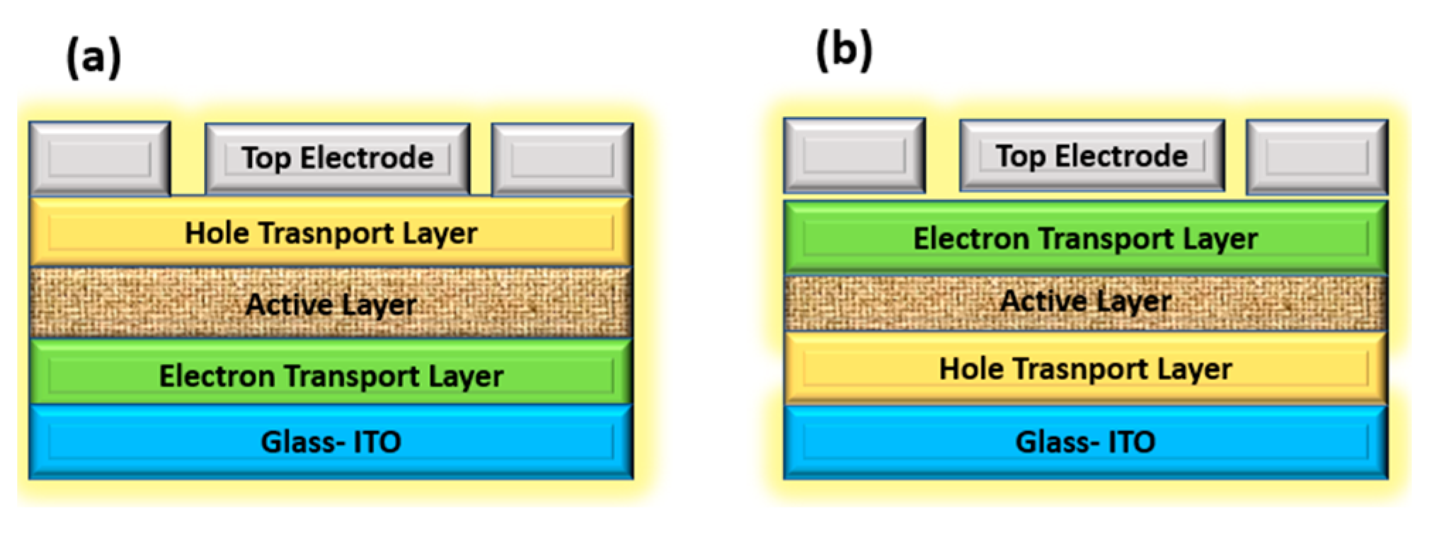
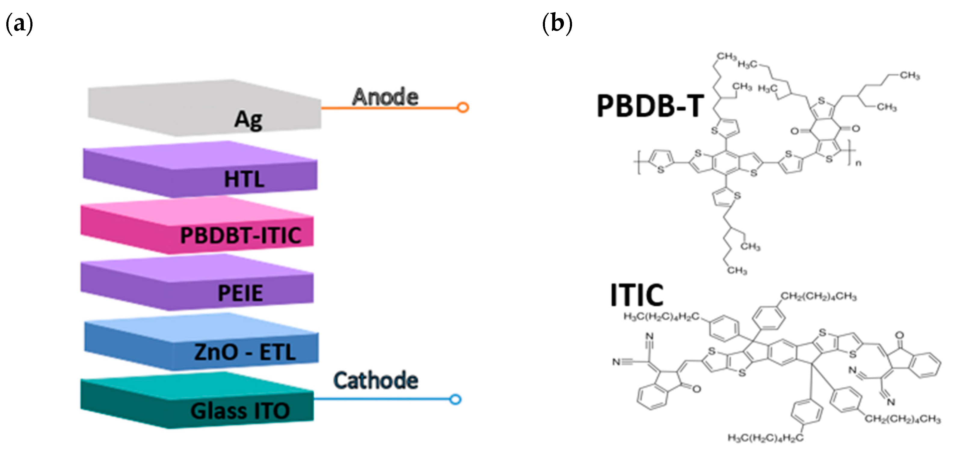
2.2. Device Fabrication

The device architecture under consideration is structured as follows: it begins with a glass substrate of 2.5 × 2.5 cm2 coated with indium tin oxide (ITO) with a sheet resistance of 10 Ω/sq as the transparent conducting electrode. The ITO substrate is patterned by a ps UV laser. On top of the ITO, there is a layer of zinc oxide (ZnO), which serves as an electron transport material. Over the ZnO layer, a polymeric material, polyethylenimine ethoxylated (PEIE), is applied to enhance the interfacial properties and charge transport [42]. This is followed by a blend layer, which typically contains the active organic materials in an organic photovoltaic device. Above the blend layer is situated the hole transport layer (HTL), and the device concludes with a top electrode made of evaporated silver (Ag). The inverted configuration of device architecture along with chemical structure of the blended PBDB-T as the doner and ITIC as the acceptor is schematically shown in Figure 2a,b.
We used the PEDOT HTL Solar as a reference in the inverted device configuration with respect to the various deposition technologies of diluted WO3. The role and optimization of WO3 as the HTL in each system will be discussed below.
Patterned ITO/glass substrates were cleaned according to the following methodology: First, a manual cleaning process with a diluted soap solution, LABWASH® PREMIUM extra 1% (VWR International Srl, Milan, Italy) in aqueous solution, was performed. As a second step, we removed the soap residue via rinsing with purified water. Afterward, the substrates were placed inside a beaker filled with D.I. water and were placed inside an ultrasonic bath for 15 min in D.I. water. The substrates were then dried with a N2 air gun and sonicated in acetone solution for 15 min, dried with a N2 air gun and sonicated in 2-propanol for 15 min. The substrates were finally exposed for 15 min inside the UV Ozone 218 Cleaner L2002A3 (OSSILA, Leiden, Netherlands) to clean organic residues and to improve the wettability and the performance of the first layer.
After the cleaning steps, every deposition in the ITO/ZnO/PEIE/PBDB-T:ITIC stack was carried out under inert conditions inside the Labstar Glovebox (MBRAUN, Garching, Germany). ZnO ink was deposited above the ITO substrates by spin coating at 2000 rpm for 45 s and annealed at 110 °C for 10 min. Then, the PEIE 0.1% interlayer was deposited by spin coating at 5000 rpm for 45 s and annealed at 110 °C for 10 min. After these steps, the active layer PBDB-T:ITIC was deposited by spin coating with 2000 rpm for 45 s and annealed at 110 °C for 10 min. These are the common steps for every cell fabrication. After the HTL deposition, 100 nm of Ag contact is deposited by a metal evaporator, using a mask that defines an active area of 0.12 cm2.

2.2.1. HTL Solar PEDOT:PSS Deposition

To improve the wettability of the active layer, 2-propanol was spin-coated above the blend at 4000 rpm for 45 s and dried at 110 °C for 10 min before the PEDOT:PSS HTL Solar was added [18]. After this preconditioning step, diluted PEDOT:PSS HTL Solar (1:5) with 2-propanol was dropped on the blend surface and left for 20 s to improve the spreading and wetting effect [38] and then spin-coated at 3000 rpm for 45 s and annealed at 110 °C in the glovebox.

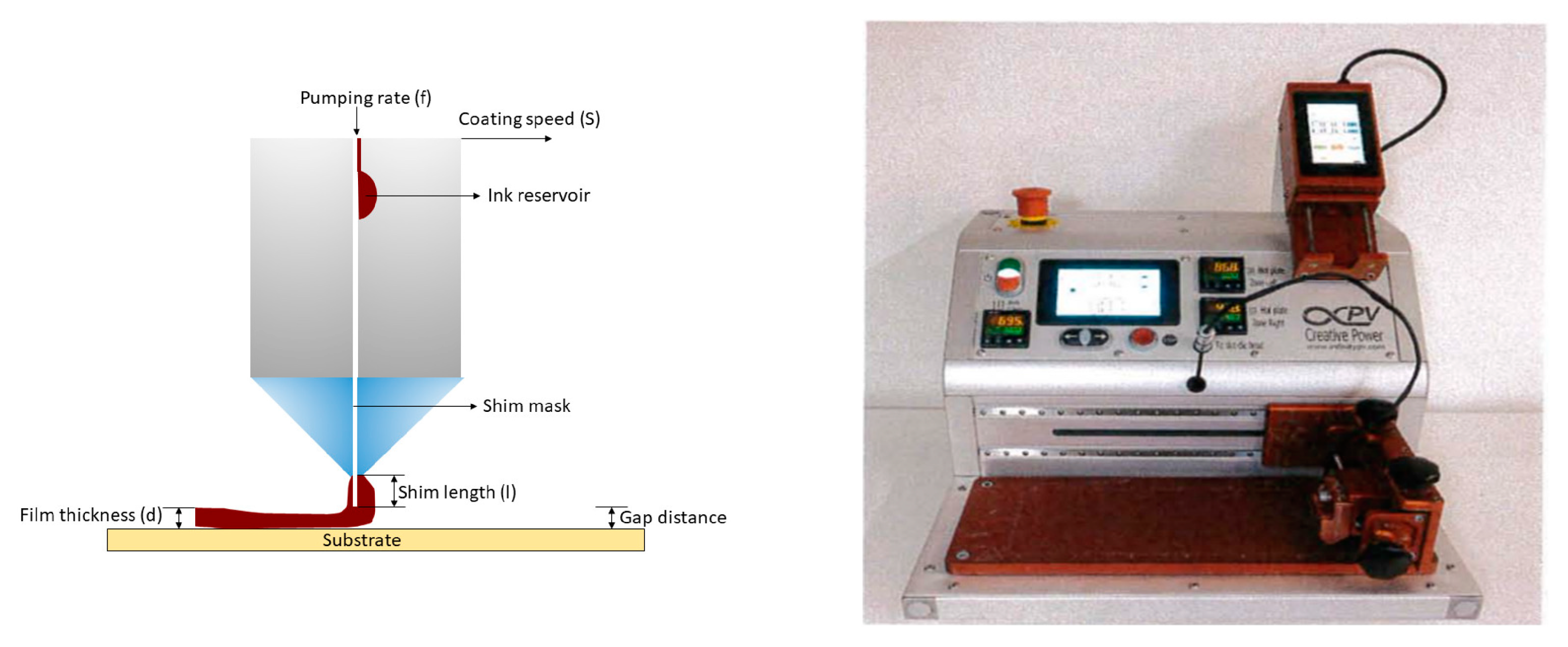
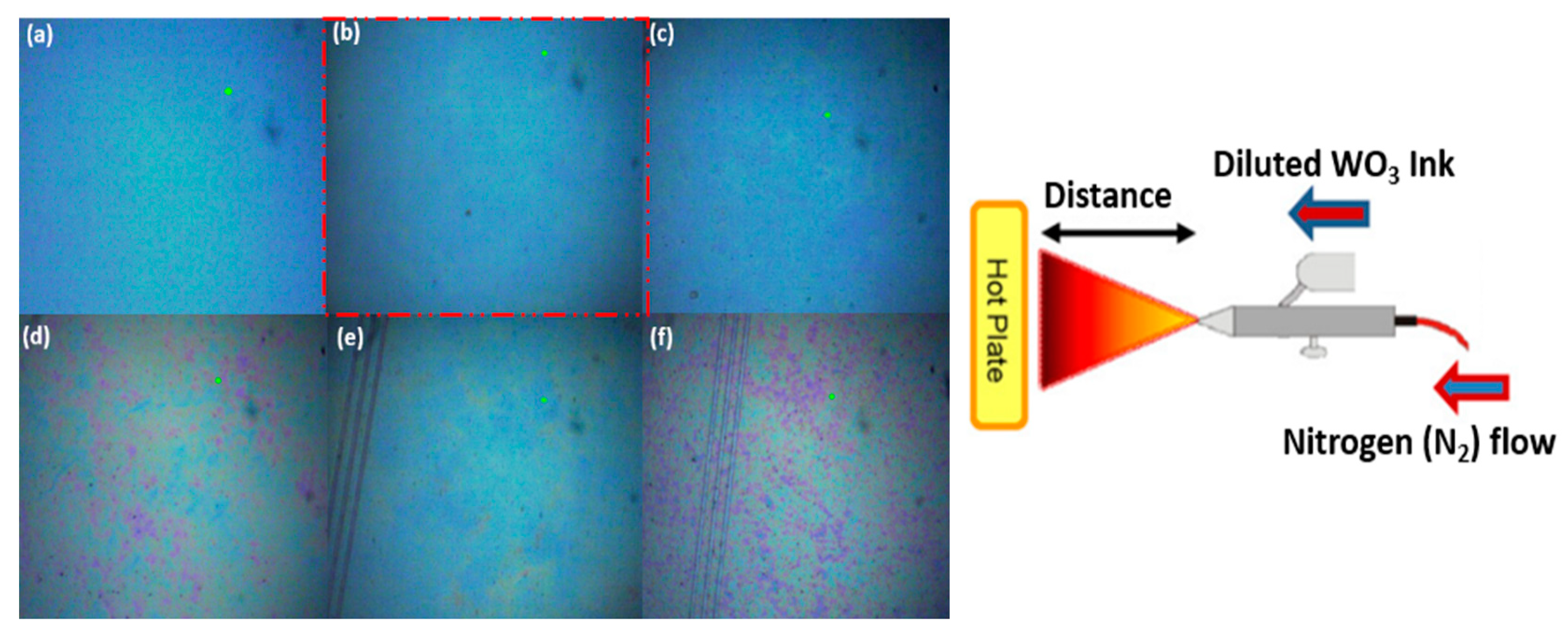
2.2.2. HTL WO3 Deposition

To deposit WO3, we optimized the parameters using spin coating, slot-die and spray coating technologies.
Spin coating is commonly used for an accurate thin-film control and deposition. The balancing between centripetal forces and surface tension provides a fast and repeatable process of thin film coating, adopted both in the industry and in research labs. It is commonly considered a reference process to control the quality of other printing methods. We explored the deposition of WO3 via spin coating considering different dilution ratios to find its optimal concentration as a HTL layer in the solar cell stack.
Slot-die coating is widely used and well suited for the deposition of solution-processable solar cell thin film layers. This technology is a highly scalable technology, enabling uniform thin film coating with a low operational cost and minimal material waste. Reference parameters for WO3 deposition are 0.05 mL/min of pumping flow with 0.3 m/min coating speed. Figure 3 shows the schematic deposition of slot-die coating (left) and the table-top coater used in this work (right).
Spray coating includes several independent steps, such as liquid precursor atomization, in-flight droplet evaporation, and the impact on the substrate, where the spreading, drying, and adhesion of the material take place [43,44,45]. The spray-coating set-up was developed in a conventional environment (air) under chemical hood in a clean room. The spray-coating was a simple dual-action commercial airbrush AG1 (MECAFER, Tours, France) supplied by a nitrogen line and fixed on a mechanic arm. After the spray deposition of the WO3, the samples were annealed at different temperatures for 10 min in a hot plate. Also, the aperture of the spray coater was studied to optimize the depositing conditions. Every deposition was made 15 cm away from the substrate for 5 s with a flow rate of 50 µL/s.

2.3. Characterization

J−V measurements of the OSCs were performed with the Class-A Sun Simulator (Abet Technologies, Inc., Milford, CT, USA) equipped with an AM1.5G filter. The calibration of the Sun Simulator was conducted by using a Si-based reference cell (RR-226-O, RERA Solutions, Nijmegen, The Netherlands) to obtain a 1 sun illumination condition. The Arkeo platform (Cicci Research s.r.l., Grosseto, Italy) was used for J−V characterization and for MPPT. A voltage step of 20 mV/s and a scan rate of 200 mV/s were set. The EQE characterization was performed with an Arkeo system (Cicci Research s.r.l.) with a 150 W xenon lamp and a double grating (300 to 1400 nm). A calibrated Si photodiode was used for incident light calibration prior to the EQE measurement. An UV–VIS spectrophotometer UV-2550 (Shimadzu, Kyoto, Japan) equipped with an integrated sphere was used for the acquisition of absorbance spectra. The spectra from 200 nm to the NIR region were acquired with an UV–vis-NIR V-630 Double Beam spectrophotometer (Jasco, Tokyo, Japan) equipped with a single monochromator.
X-ray diffraction measurements (XRD) were performed upon the WO3 samples in order to evaluate their structural properties. The experimental set-up exploits a Panalytical Empyrean X-ray diffractometer equipped with a line PixCel 3D detector, a Cu-anode tube X-ray source (Kα1 = 1.54060 Å, Kα2 = 1.54443 Å), incident divergent slits of 0.2177° and a flat sample holder for thin films. The XRD patterns were collected in the Bragg–Brentano configuration, spanning the 5°–90° 2θ angular range with a step size of 0.0130°, setting the generator parameters at 45 mA and 40 kV.
An in-house designed atomic force microscope (AFM) set up with a 30 μm × 30 μm scanner was used to investigate the morphological surface characteristics of the films. Images representative of several portions of each sample were collected at different dimensions, ranging between 30 μm × 30 μm and up to 10 μm × 10 μm, with a resolution of 500 points/image. Al-coated standard tapping AFM probes (Nanosensors, Neuchatel, Switzerland) were used to probe the surfaces in non-contact mode.
Micro-Raman measurements were performed using a In Via spectroscope (Renishaw, Wotton-under-Edge, UK). All spectra were acquired using a 457 nm laser source and a 2400 lines/cm edge filter, setting the laser power to 50%, an acquisition time of 2 s per point and 50 acquisitions for each pattern.

3. Results and Discussions

We compared tungsten trioxide (WO3) as a hole transport layer (HTL) in inverted organic photovoltaics (OPVs) using various deposition techniques, including spin coating, slot-die coating, and spray coating. These investigations aimed to assess the impact of deposition methods on the performance and efficiency of OPV devices. Spin coating is a widely adopted technique known for its precise control over film thickness and uniformity [46]. Slot-die coating is valued for its scalability and potential for high-throughput production [47]. Spray coating, on the other hand, offers the advantage of fast and continuous deposition [47]. These comparative studies examine how each technique affects the film quality, device stability, and overall OPV efficiency, contributing to the ongoing development and optimization of inverted OPV technologies.

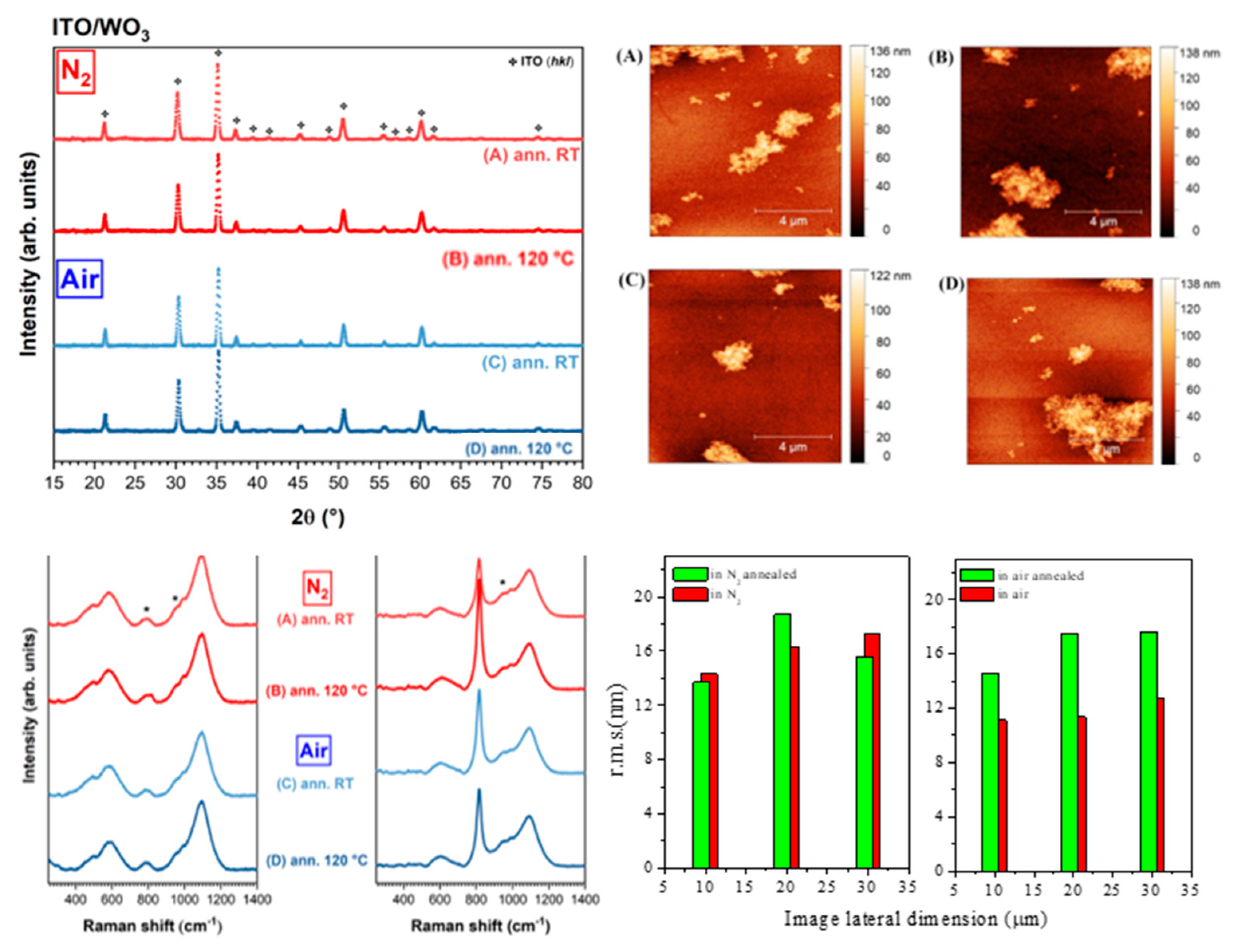
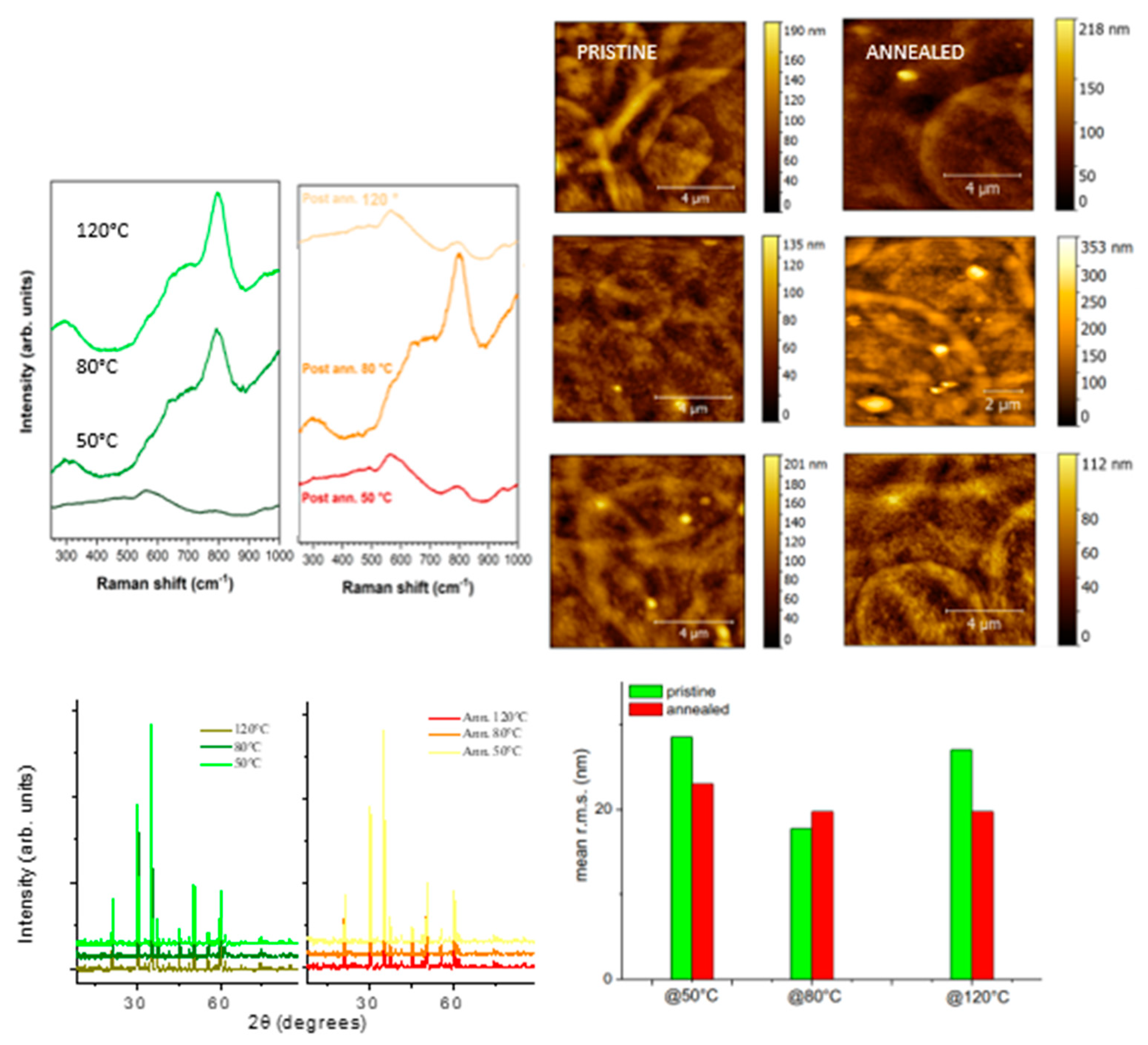
3.1. Pure WO3 Films: Structural and Morphological Characterization

The surface morphology and structure are critical parameters in producing thin WO3 films, via different deposition methods and annealing treatments, to be inserted as the HTL in inverted OPVs. Indeed, different morphologies/structures for bare WO3 and consequently different cell efficiencies have been reported depending on the preparation methods used [48,49,50]. For this reason, the slots of pure WO3 films deposited on glass/ITO where preliminarily characterized to optimize deposition conditions/post deposition treatments.
XRD, Raman and AFM results for the slot-die-deposited samples are reported in Figure 4. From the experimental diffractograms, no evidence of crystalline WO3 is found regardless of the annealing temperature, as confirmed by the absence of the peaks around 23°, which is the typical fingerprint of the WO3 crystalline phases [51,52,53].
The most intense reflections in the XRD patterns, marked by a symbol, are attributed to the ITO film [54,55]. Despite the fact that WO3 is not detected by XRD, the characteristic Raman band associated with the O–W–O stretching modes [53] is still present around 800 cm−1, as visible in Figure 4 where the micro-Raman spectra of regions of the clean sample surface/surface with agglomerates are respectively shown in the left and right panel. Interestingly, the Raman spectra collected upon the agglomerates show features compatible with a higher crystalline character, which is slightly improved by annealing, as confirmed by the sharp signal around 810 cm−1 and by the appearance of the small shoulder around 710 cm−1 after annealing at 120 °C and 150 °C (curves (C) and (D) in the left panel) [56]. It is worth mentioning that the intensity of the shoulder at 710 cm−1 is still very small and that the Raman spectra all share a common feature around 950 cm−1, which is characteristic of amorphous WO3 films [57]. All these observations, together with the XRD suggest that the slot-die-deposited WO3 films are characterized by a prevalent amorphous general character.
AFM images—ranging from 10 μm × 10 μm to 30 μm × 30 μm—were collected (the smallest image is reported in Figure 4 for each film) upon different surface regions for each sample, and the statistical roughness analysis was evaluated. The thus-obtained RMS values deduced from all collected images (see Figure S1 Supplementary material) are reported in a figure; it is evident that the best film morphology both in terms of the average roughness (1.5 ± 5 nm) and uniformity is obtained when 120 °C annealing is performed.
Subsequently spin-coated WO3 films deposited in different atmospheres (N2/air) and annealed at different temperatures were investigated as previously discussed. As reported in Figure 5, the XRD and Raman characterization of the spin-coated WO3 samples reveal a prevalent amorphous character of the WO3 films as already observed for the samples deposited via slot die, with no evidence of the formation of crystalline WO3.
AFM images (10 × 10 μm) suggest that morphology is affected by WO3 agglomerates independent of the deposition conditions, and the statistical roughness analysis is also reported, showing a general surface uniformity, with WO3 agglomerates being randomly but uniformly distributed (RMS almost constant independent of the image dimension); quite high roughness values are observed, ranging from ≈12 to ≈17 nm. It is worth noticing that when deposition occurs in nitrogen, annealing does not affect the roughness values, while the RMS values are enhanced when the same treatment is performed in air. The statistical roughness analysis performed upon all collected images (see Figure S2 Supplementary material) shows a general improvement in surface uniformity with respect to the slot-die samples, but higher roughness values are obtained. The clear changes found in the micro-Raman spectra collected upon the agglomerates (an indication of a crystalline structure within the agglomerates) are indicative of compositional/structural inhomogeneities in the spin-coated films.
Finally, spray-coated films deposited at 50 °C, 80 °C and 120 °C were characterized (no post-deposition treatment and with post-deposition annealing) and the results are reported in Figure 6. XRD and Raman characterization reveal an amorphous character of the WO3 films as already observed for the films obtained by different deposition techniques. All AFM images (see Figures S3–S5) display round haloes (due to the spray deposition methods) and a smaller globular-shaped texture attributed to WO3 particles both in the pristine and annealed films (10 × 10 μm images are reported in Figure 6: left side shows the pristine samples/right side shows the annealed films). The texture is not affected by annealing. The film texture is quite non-homogeneous (mean RMS values increasing as the image dimension increases, see Figure S6, Supplementary Information) and the roughness values are higher than those deduced for WO3 films obtained by slot-die and spin coating deposition techniques. However, the statistical analysis performed upon all collected images suggest that annealing enhances the surface homogeneity, reducing the presence of defects except for the film annealed at 80 °C. The best film morphology improvement is obtained when depositing WO3 at 120 °C and performing the post-deposition treatment at the same temperature.

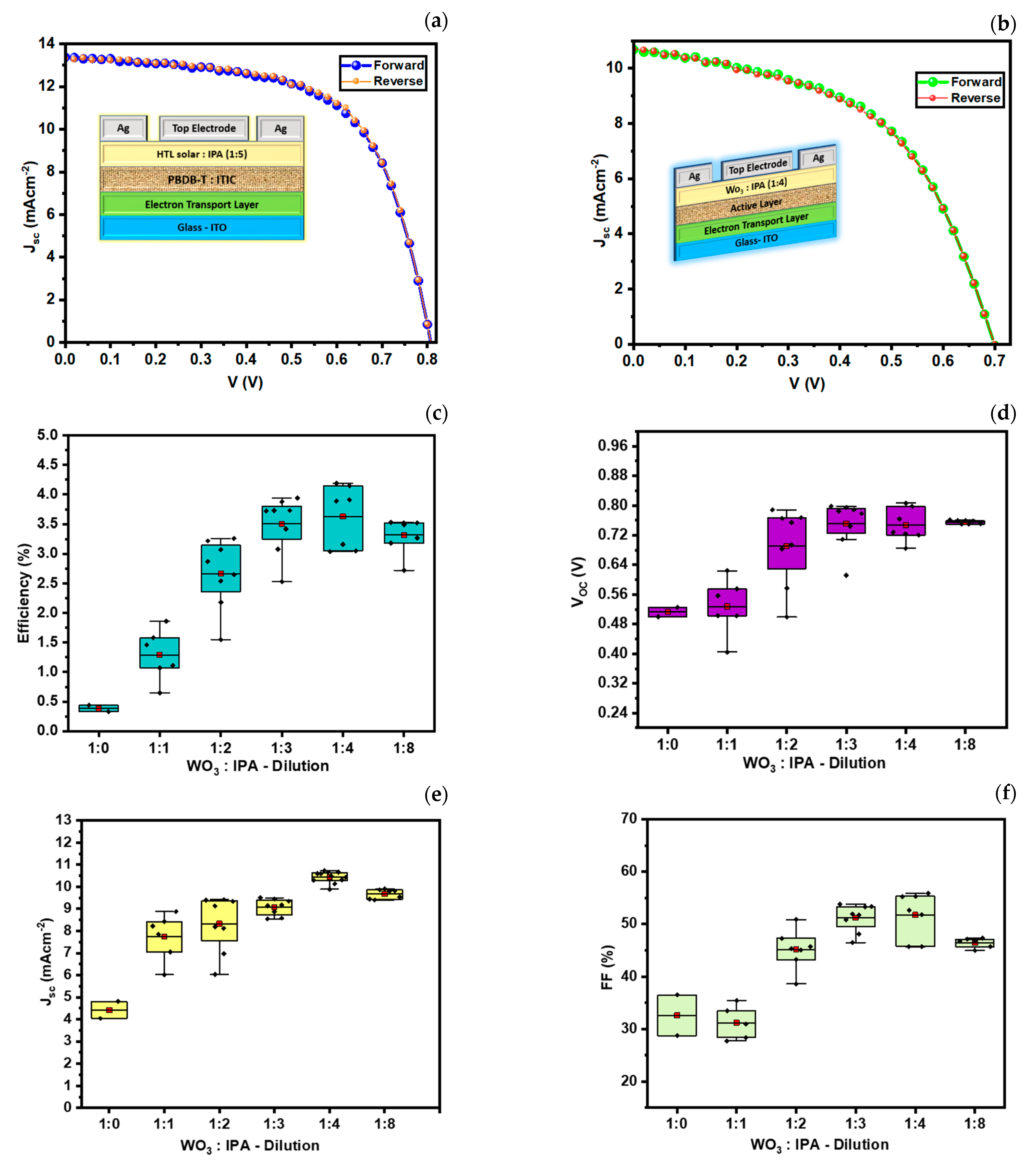
3.2. WO3 as the HTL in Inverted OPVs via Spin Coating

Figure 7a shows the short-circuit current density–open-circuit voltage (JSC-VOC) characteristic under the AM 1.5G sun simulator of the diluted HTL solar PEDOT:PSS (1:5) with isopropanol employed as a reference. The dilution of a HTL with organic solvents such IPA and ethanol improves the wettability, interfacial compatibility, hole transporting properties and hence the performance of the device [38]. However, due to its acidic nature, hygroscopicity, and environmental sensitivity, PEDOT:PSS as a HTL limits the stability of organic solar cells. In this study, we replace PEDOT:PSS aqueous solution with WO3 and explored the role of diluted WO3 in an inverted OPV configuration (ITO/ZnO/PBDBT-ITIC/WO3)/Ag to solve the wettability/hydrophobic issue of the surface of the BHJ.
Figure 7b shows the JV curve of the best working devices at the optimal dilution of spin-coated WO3 diluted (1:4) with IPA. Figure 7c–f show the statistical analysis of PV parameters for various WO3 dilutions in IPA applied via spin coating and annealed at 120 °C. The average value over two samples of diluted WO3 in each concentration are summarized in Table 1.
Through the statistical representation of PV parameters, we analyzed the impact of incorporating diluted WO3 as a HTL on the wettability of the active layer of the BHJ (PBDB-T: ITIC), device performance in term of efficiency, fill factor, open-circuit voltage, and short-circuit current density. We have seen an increasing trend in the PV parameter as a function of different concentrations and observed the best dilution of WO3 (1:4) with IPA. Indeed, AFM images were collected upon the (1:4) WO3 120 °C annealed film, and a much more homogenous morphology was observed, as shown in Figure 8. No visible clusters are detected in comparison with the pure spin-deposited tungsten trioxide film and the mean roughness value is very much reduced, being ≈5 nm independent of the image dimension.
This demonstrated that the dilution in the HTL in inverted device configurations improve the wettability of the BHJ, the interfacial compatibility, the quality of the film and device performance [58]. This information is valuable for optimizing the hydrophobicity of the BHJ, the hole transporting properties and hence the performance of inverted OPVs.

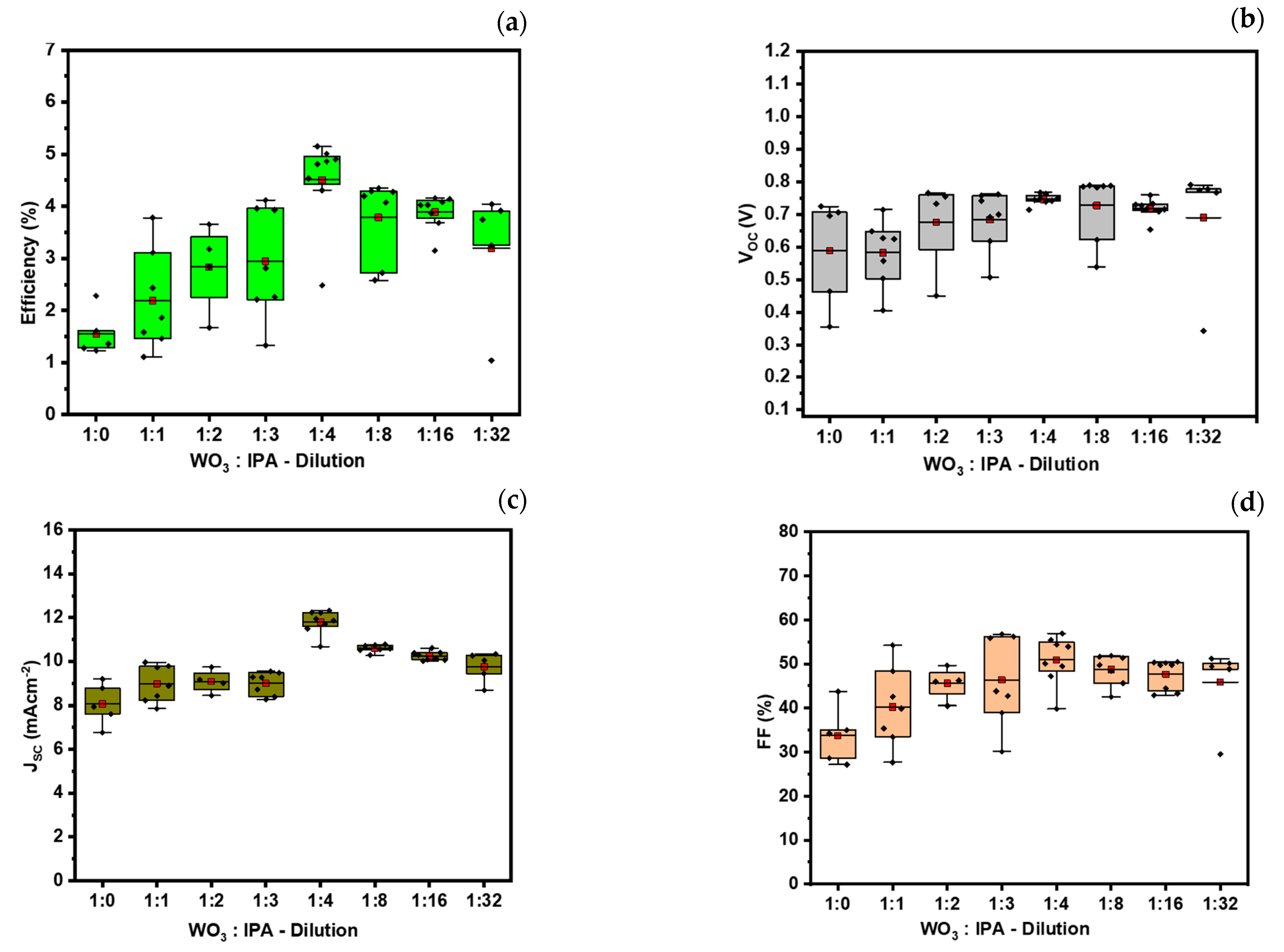
3.3. WO3 as a HTL in Inverted OPVs via Slot Die and Spray Coating

Here, we focus on examining the role of both pure and diluted WO3 as the HTL in inverted OPVs via slot-die and spray coating techniques. This approach aims to understand how the different concentrations of WO3 with IPA improve the wettability of the BHJ, the stability, and key device parameters such as the power conversion efficiency, VOC, JSC and FF and assess their feasibility for large-scale production. The findings will contribute to optimizing WO3 as a HTL in inverted OPV devices for enhanced stability and scalability.
Figure 9a–d show the statistical analysis of the performance in term of PV parameters as a function of various slot-die-coated WO3 diluted in IPA, which demonstrates that the best performing dilution of WO3 is 1:4, the same as what we observed in the case of the spin-coated sample.
To investigate the role of the deposition of diluted WO3 via spray coating on the device performance, a comparison of the spin-coated, and spray-coated WO3 was carried on the polymer BHJ: PBDB-T: ITIC in air. To optimize the roughness and uniformity of the deposition of diluted WO3 film on the blend, we observed the optical images of spin-coated WO3 (1:4) on glass ITO as a reference and spray-coated WO3 on glass ITO with different process parameters such as the distance between the sample and airbrush, the spray duration, and the flow rate.
The details for the deposition of WO3 on glass ITO with different spray conditions are shown in Figure 10 (left): (a) WO3 (1:4)—spin coating as a reference; (b) WO3 (1:8)—spray coating: 5 s, flow rate of 50 µL/s, 15 cm; (c) WO3 (1:8)—spray coating: 3 s, flow rate of 37.5 µL/s, 10 cm; (d) WO3 (1:8)—spray coating: 5 s, flow rate of 37.5 µL/s, 10 cm; (e) WO3 (1:4)—spray coating: 5 s, flow rate of 37.5 µL/s, 10 cm; and (f) WO3 (1:8)—spray coating: 5 s, flow rate of 50 µL/s, 15 cm.
The comparison indicated that the optical uniformity of spin-coated WO3 (1:4) and spray-coated WO3 (1:8) films with the process parameters, spray duration (5 s), flow rate (50 µL/s), and distance of the airbrush with respect to the target sample (15 cm), matched well compared to other process parameters of spray-coated WO3 films. Therefore, these optimal spray conditions were adopted in the spray coating of WO3 at the top of the BHJ.
The comparison of device performance in term of JV analysis, IPCE, UV-Vis and absorbance spectra of the optimized deposition of WO3 over the blend for spin coating, slot-die coating and spray coating technologies will be discussed in Section 3.4.

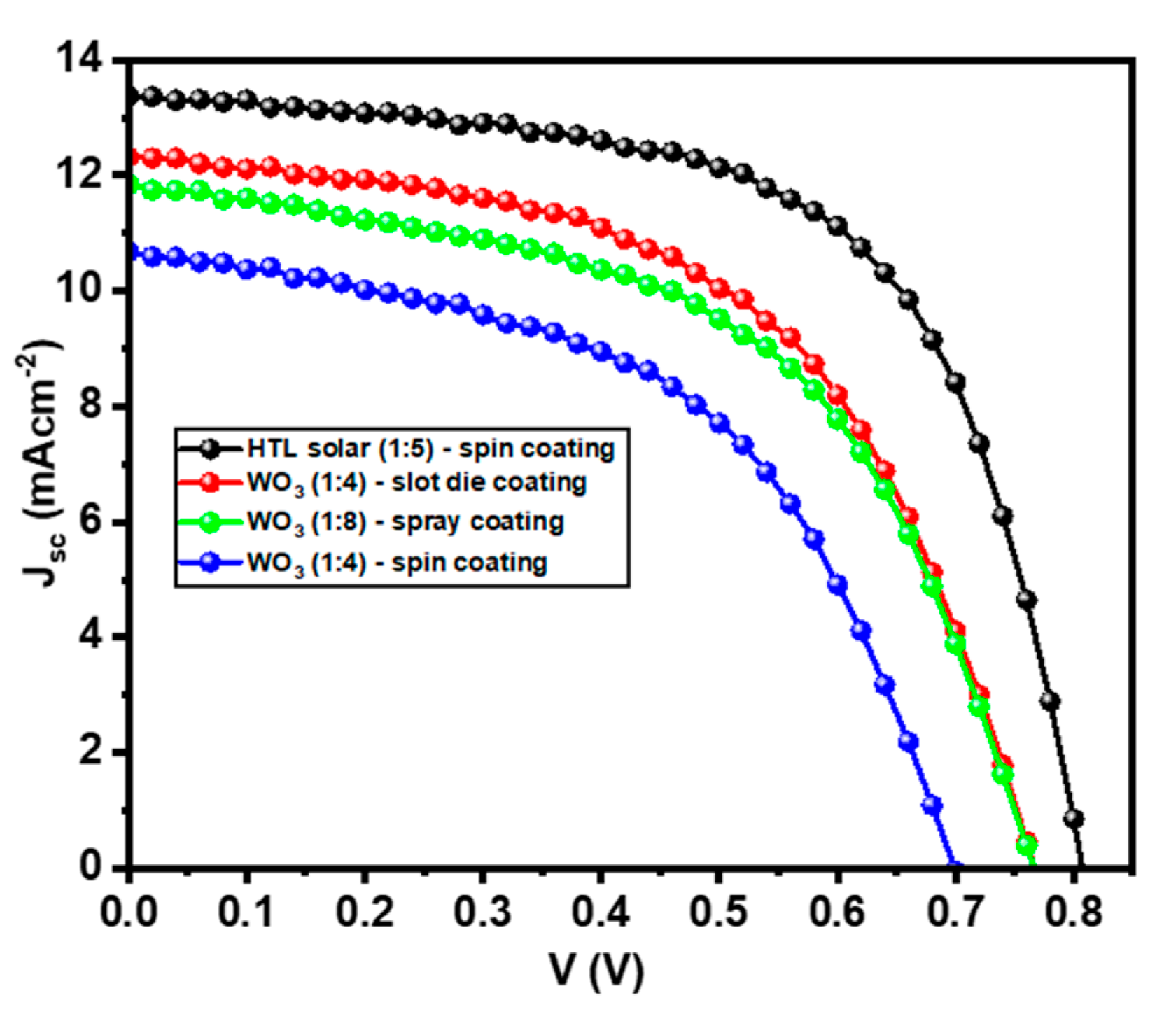
3.4. Technology Comparison

In the previous section, we investigated the role of dilution in PEDOT:PSS HTL Solar as a reference device and WO3 as the HTL in inverted OPVs by using three different techniques individually. In this section, we present a comparison of the device performance of the HTL solar as a reference and diluted WO3 as a HTL using three different deposition technologies: spin coating—WO3 (1:4), slot-die coating—WO3 (1:4), and spray coating—WO3 (1:8). The combined JV curve of the best working devices for the reference case and the optimal dilution of spin-coated, slot-die coated, and spray-coated WO3 is shown in Figure 11. A statistical analysis of PV parameters as a function of the various deposition techniques is shown in Figure 12a–d.
The evaluation of the J–V performance in devices utilizing PEDOT:PSS and WO3 as HTLs demonstrates that PEDOT:PSS exhibits superior results, with enhanced photovoltaic parameters such as JSC and the power conversion efficiency. This advantage can be attributed to the lower resistive losses and lower absorption coefficient of PEDOT:PSS within the visible spectrum compared to other polymers and inorganic HTLs [59]. This attribute enables the active layer of the solar cell to capture a greater number of photons, leading to an increased JSC and an overall improvement in device efficiency. However, due to the stability issues in the case of PEDOT:PSS, we explored the optimization of WO3 as a HTL in terms of device performance and stability via spin coating, slot-die coating and spray coating technologies. The J–V characteristics revealed that slot-die coating resulted in the highest performance, followed by spray coating, with spin coating technology exhibiting the lowest performance. The results of the PV parameters are summarized in Table 2, indicating that a more efficient carrier extraction is obtained in the case of slot-die- and spray-coated diluted WO3. The photovoltaic data are reported considering an average over at least eight devices for each case. The reliability and yield of the different methods of deposition have been verified repeating the fabrication of the same set of samples for each case at least twice with the same manufacturing conditions, obtaining the same device yield and results with the same trend, within the error range of the data presented in Table 2.
To confirm the JV parameters, specifically the short-circuit current density (JSC) value observed from JV curves of the reference device and diluted WO3 processed by three different techniques and absorption, an IPCE measurement and UV-Vis absorbance were performed, and the corresponding observations are presented in Section 3.4.1.

3.4.1. Analysis of IPCE, Absorbance Spectra and Thickness of Active Layer

This study involves a comparative analysis of inverted OPVs by examining the IPCE and integrated current density to confirm the JSC values observed via a sun simulator of each device where HTLs (HTL solar and diluted WO3) were processed by three different techniques while correlating them with the absorbance spectra. This aims to understand the influence of deposition methods on the device’s optical and electrical characteristics.
Figure 13a shows that all devices exhibit relatively consistent profiles in their IPCE spectra, and there is a strong agreement between the photocurrent values calculated from the integrated EQE and those determined through J–V curve testing. The deviation of JSC values from the JV curve and integrated IPCE spectra are summarized in Table 3. The deviation in the case of spin-coated WO3 (8%) is higher than the slot-die-coated (5.8%) and spray-coated (2.7%) devices. However, the deviation value in each case is in the range, which is observed in OPVs, although this can vary based on the precision of the measurement equipment and the nature of the materials and device being studied [60].
To correlate the electrical performance of the device with PBDB-T: ITIC and diluted WO3 as the HTL dispersed by various deposition techniques, the optical absorption of the device (ITO/ZnO/PEIE/PBDB-T:ITIC/HTLs) was examined, as shown in Figure 13b. The absorption spectra of all stacks showed the strong absorption of the device in the range of around 500–750 nm, with high and less intense peaks around 632 nm and 695 nm, respectively. The device based on the HTL solar has a higher absorption and hence performance compared to the diluted WO3. The higher absorption in PEDOT:PSS as the HTL and corresponding device performance is due to the lower value of the absorption coefficient of PEDOT:PSS in the visible range of the solar spectrum compared to other polymers and inorganic hole-transporting layers. This property allows the active layer of the device to capture more photons, boosting the short-circuit current density JSC and enhancing the overall device efficiency [59]. Furthermore, the absorption in the case of the WO3–slot-die coating higher than the WO3–spray and spin-coated techniques. The absorption spectra in each case are consistent with the device performance in terms of JV curves and IPCE measurements, which are higher in the WO3–slot-die and spray-coated samples compared to the WO3–spin-coated samples. Furthermore, each device has a strong absorption in the range of 500–700 nm, which is consistent with the complementary absorbance spectra between PBDB-T:ITIC [60,61], indicating that ITIC molecules exhibit strong and wide-ranging absorption properties, spanning from the visible spectrum to the near infrared, with their peak absorption occurring at 700 nm.
To explore the thickness requirement in printable OPVs, the thickness of full cell stacks with diluted HTL solar and WO3 by three different techniques were investigated via a profilometer (Dektak 150), as shown in Table 4. Considering that the ETL (ZnO/PEIE) and HTL are 20 nm each, the thickness of the active layer is in the range of 100 nm, consistent with the optimal range of the thickness reported in printable OPVs. The highest PCE in polymer solar cells using non-fullerene acceptors (NFAs) are typically attained when the active layer has a thickness ranging from approximately 90 to 120 nm [62,63].

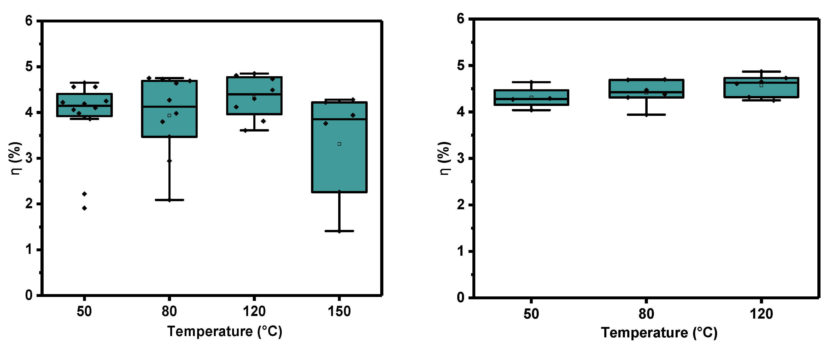
3.4.2. Role of Annealing Temperature in Slot-Die- and Spray-Coated WO3

To investigate the impact of annealing temperatures on the performance of slot-die- and spray-coated diluted WO3 as a HTL in photovoltaic devices, we conducted a detailed morphological and J-V analysis. The device efficiency is shown in Figure 14 (left) for HTL solar, spin- and slot-die- and (right) for spray-coated samples, demonstrating that the highest performance is achieved at an annealing temperature of 120 °C, which serves as an optimal and critical temperature for all three coating technologies (we set the temperature of annealing for the WO3 deposited by spin coating to 120 °C), in perfect agreement with the morphological information deduced by means of the AFM upon diluted annealed WO3 films.
Indeed, a strong improvement in surface texture is detected, as visible in Figure 15 where 5 × 5 and 10 × 10 μm AFM images are presented. Film surfaces are clearly now much more homogenous with respect to their pure tungsten oxide counterparts deposited by means of the same techniques (and same annealing). Diluted slot-die WO3 annealed at 120 °C shows a mean RMS ≈ 7.0 nm, while for spray-coated diluted films, the RMS is ≈9.5 nm. Moreover, independent of the deposition technique, the surfaces are now homogenous, no agglomerates are detected and the texture is characterized by small globular structures, characteristic of tungsten trioxide [64,65].
This finding is particularly significant because, in the case of slot-die-coated WO3, annealing at 150 °C results in a notably lower device performance as well as in a lower film quality as previously discussed, underlining the importance of precise temperature control in the annealing process to control the structure and morphology of the HTL.

3.5. Stability

To investigate the impact of WO3 on cell stability, we performed a light soaking test on stabilized unencapsulated cells kept at MPPT. A clear improvement in cell stability is observed in Figure 16 with respect to the HTL solar reference cell, especially for the slot-die- and spray-coated samples. We attribute this improvement to the hygroscopic nature of the PEDOT HTL layer, compared to the WO3 HTL.

4. Conclusions

In this study, we have performed a comparative analysis of the role of the techniques for the deposition of WO3 as a HTL in inverted OPVs. The evaluation of the JV performance in devices utilizing PEDOT:PSS and WO3 as HTLs demonstrates that PEDOT:PSS exhibits superior results, with enhanced photovoltaic parameters such as JSC and the power conversion efficiency.
This advantage can be attributed to the lower resistive losses and lower absorption coefficient of PEDOT:PSS within the visible spectrum compared to other polymers and inorganic HTLs. However, due the known stability issues in the case of PEDOT:PSS, we explored the optimization of WO3 as a HTL in term of device performance and stability by spin coating, slot-die coating and spray coating technologies. The J–V characteristics revealed that slot-die coating resulted in the highest performance, followed by spray coating, with the spin coating technology exhibiting the lowest performance.
A morphological characterization revealed that when pure WO3 films are deposited via different deposition techniques, amorphous tungsten trioxide is obtained, which is characterized by quite a non-homogeneous and rough film surface. Annealing procedures favor the morphology improvement in terms of lower roughness values and improved homogeneity, and in particular, at 120 °C, annealing the best trioxide films are obtained, independent of the deposition methods.
However, when diluted tungsten trioxide films are produced and annealed at 120 °C, the surface morphology is drastically improved, with the structure still being amorphous. A smooth surface texture characterized by globular-shaped grains is obtained, without defects nor agglomerates. This improved morphology positively affects the efficiency of the trioxide when complete devices are produced.
These morphological results are consistent with the findings of diluting WO3 in IPA as an effective route to improve device processability and performance, when using WO3 as HTL in inverted OPVs. Future results will investigate the role of WO3 in high performing BHJs such as the ones based on PM6 and Y-family NFAs.

Supplementary Materials

The following supporting information can be downloaded at: https://www.mdpi.com/article/10.3390/en17040814/s1. Figure S1. Comparison of AFM images ranging from 10 μm to 30 μm lateral dimension collected upon WO3 Slot Die deposited films and differently annealed: (A) 50 °C; (B) 80 °C; (C) 120 °C; (D) 150 °C. Figure S2. Comparison of AFM images ranging from 10 μm to 30 μm lateral dimension collected upon WO3 films deposited by spin coating in nitrogen (line A pristine sample- line B annealed) and in air (line C pristine sample- line D annealed). Figure S3. AFM images representative of the whole WO3 spray deposited pristine sample@50 °C and annealed @50 °C: (A) (30 × 30) µm, (B) (20 × 20) µm, (C) (10 × 10) µm and (D) (5 × 5) µm. Figure S4. AFM images representative of the whole WO3 spray deposited pristine sample@80 °C and annealed @80 °C: (A) (30 × 30) µm, (B) (20 × 20) µm, (C) (10 × 10) µm and (D) (5 × 5) µm. Figure S5. AFM images representative of the whole WO3 spray deposited pristine sample@120 °C and annealed @120 °C: (A) (30 × 30) µm, (B) (20 × 20) µm, (C) (10 × 10) µm and (D) (5 × 5) µm. Figure S6. Mean r.m.s. values calculated on all the acquired images (red bars) are shown as a function of the deposition temperature of each film, and compared with the annealed counterpart (green bars).

Author Contributions

Conceptualization, A.R., F.B. and B.P.; AFM characterization, B.P., A.G. and F.R.R.; device fabrication and characterization, A.U.R., A.E.A.-Q., G.S., E.C., H.J. and G.P.; discussion of results, writing, review and editing A.R., A.U.R. and A.E.A.-Q. All authors have read and agreed to the published version of the manuscript.

Funding

This work has been partially supported by the ITA-NTN “Integrated Terrestrial And Non-Terrestrial Networks” project under the RESTART “RESearch and innovation on future Telecommunications systems and networks, to make Italy more smart” initiative of the PNRR.

Data Availability Statement

Data are contained within the article.

Acknowledgments

The authors are grateful to Dr. Marco Guaragno (SpecX Lab ISM CNR) for his technical support with the XRD experiments.

Conflicts of Interest

Author Emanuele Calabrò is currently employed by the company Greatcell Solar Italia. The remaining authors declare that the research was conducted in the absence of any commercial or financial relationships that could be construed as a potential conflict of interest.

References

  1. International Renewable Energy Agency (IRENA) Headquarters. Future of Solar Photovoltaic; International Renewable Energy Agency: Abu Dhabi, United Arab Emirates, 2019. [Google Scholar]
  2. Zhang, H.; Yu, Z.; Zhu, C.; Yang, R.; Yan, B.; Jiang, G. Green or not? Environmental challenges from photovoltaic technology. Environ. Pollut. 2023, 320, 121066. [Google Scholar] [CrossRef]
  3. Fukuda, K.; Yu, K.; Someya, T. The future of flexible organic solar cells. Adv. Energy Mater. 2020, 10, 2000765. [Google Scholar] [CrossRef]
  4. Giannouli, M. Current status of emerging PV technologies: A comparative study of dye-sensitized, organic, and perovskite solar cells. Int. J. Photoenergy 2021, 2021, 6692858. [Google Scholar] [CrossRef]
  5. Chen, B.; Yang, Z.; Jia, Q.; Ball, R.J.; Zhu, Y.; Xia, Y. Emerging applications of metal-organic frameworks and derivatives in solar cells: Recent advances and challenges. Mater. Sci. Eng. R Rep. 2023, 152, 100714. [Google Scholar] [CrossRef]
  6. La Notte, L.; Cataldi, P.; Ceseracciu, L.; Bayer, I.S.; Athanassiou, A.; Marras, S.; Villari, E.; Brunetti, F.; Reale, A. Fully-sprayed flexible polymer solar cells with a cellulose-graphene electrode. Mater. Today Energy 2018, 7, 105–112. [Google Scholar] [CrossRef]
  7. Solak, E.K.; Irmak, E. Advances in organic photovoltaic cells: A comprehensive review of materials, technologies, and performance. RSC Adv. 2023, 13, 12244–12269. [Google Scholar] [CrossRef] [PubMed]
  8. Ren, M.; Qian, X.; Chen, Y.; Wang, T.; Zhao, Y. Potential lead toxicity and leakage issues on lead halide perovskite photovoltaics. J. Hazard. Mater. 2022, 426, 127848. [Google Scholar] [CrossRef]
  9. Nguyen, V.H.; Papanastasiou, D.T.; Resende, J.; Bardet, L.; Sannicolo, T.; Jiménez, C.; Muñoz-Rojas, D.; Nguyen, N.D.; Bellet, D. Advances in flexible metallic transparent electrodes. Small 2022, 18, 2106006. [Google Scholar] [CrossRef]
  10. Salim, M.B.; Nekovei, R.; Jeyakumar, R. Organic tandem solar cells with 18.6% efficiency. Solar Energy 2020, 198, 160–166. [Google Scholar] [CrossRef]
  11. Wang, D.; Liu, H.; Li, Y.; Zhou, G.; Zhan, L.; Zhu, H.; Lu, X.; Chen, H.; Li, C.-Z. High-performance and eco-friendly semitransparent organic solar cells for greenhouse applications. Joule 2021, 5, 945–957. [Google Scholar] [CrossRef]
  12. Hoff, A.; Farahat, M.E.; Pahlevani, M.; Welch, G.C. Tin oxide electron transport layers for air-/solution-processed conventional organic solar cells. ACS Appl. Mater. Interfaces 2022, 14, 1568–1577. [Google Scholar] [CrossRef]
  13. Zheng, Z.; Wang, J.; Bi, P.; Ren, J.; Wang, Y.; Yang, Y.; Liu, X.; Zhang, S.; Hou, J. Tandem organic solar cell with 20.2% efficiency. Joule 2022, 6, 171–184. [Google Scholar] [CrossRef]
  14. NREL Efficiency Chart. 2023. Available online: https://www.nrel.gov/pv/cell-efficiency.html (accessed on 11 January 2024).
  15. Reb, L.K.; Böhmer, M.; Predeschly, B.; Grott, S.; Weindl, C.L.; Ivandekic, G.I.; Guo, R.; Dreißigacker, C.; Gernhäuser, R.; Meyer, A.; et al. Perovskite and organic solar cells on a rocket flight. Joule 2020, 4, 1880–1892. [Google Scholar] [CrossRef]
  16. Tu, Y.; Wu, J.; Xu, G.; Yang, X.; Cai, R.; Gong, Q.; Zhu, R.; Huang, W. Perovskite solar cells for space applications: Progress and challenges. Adv. Mater. 2021, 33, 2006545. [Google Scholar] [CrossRef] [PubMed]
  17. Güler, E.N.; Distler, A.; Basu, R.; Brabec, C.J.; Egelhaaf, H.-J. Fully solution-processed, light-weight, and ultraflexible organic solar cells. Flex. Print. Electron. 2022, 7, 025003. [Google Scholar] [CrossRef]
  18. Lee, C.; Lee, J.; Lee, S.; Lee, W.; You, H.; Woo, H.Y.; Kim, B.J. Importance of device structure and interlayer design in storage stability of naphthalene diimide-based all-polymer solar cells. J. Mater. Chem. A 2020, 8, 3735–3745. [Google Scholar] [CrossRef]
  19. Wang, D.; Zhou, G.; Li, Y.; Yan, K.; Zhan, L.; Zhu, H.; Lu, X.; Chen, H.; Li, C.Z. High-Performance Organic Solar Cells from Non-Halogenated Solvents. Adv. Funct. Mater. 2022, 32, 2107827. [Google Scholar] [CrossRef]
  20. Fan, J.Y.; Liu, Z.X.; Rao, J.; Yan, K.; Chen, Z.; Ran, Y.; Yan, B.; Yao, J.; Lu, G.; Zhu, H. High-Performance Organic Solar Modules via Bilayer-Merged-Annealing Assisted Blade Coating. Adv. Mater. 2022, 34, 2110569. [Google Scholar] [CrossRef]
  21. Sreejith, S.; Sivasankari, B. A review on P3HT: PCBM material based organic solar cells. In Proceedings of the 2022 IEEE International Conference on Nanoelectronics, Nanophotonics, Nanomaterials, Nanobioscience & Nanotechnology (5NANO), Kottayam, India, 27 April–3 May 2022; pp. 1–6. [Google Scholar] [CrossRef]
  22. Li, Y.; Huang, X.; Sheriff, H.K., Jr.; Forrest, S.R. Semitransparent organic photovoltaics for building-integrated photovoltaic applications. Nat. Rev. Mater. 2023, 8, 186–201. [Google Scholar] [CrossRef]
  23. Duan, L.; Hoex, B.; Uddin, A. Progress in semitransparent organic solar cells. Solar RRL 2021, 5, 2100041. [Google Scholar] [CrossRef]
  24. Allardyce, C.S.; Fankhauser, C.; Zakeeruddin, S.M.; Grätzel, M.; Dyson, P.J. The influence of greenhouse-integrated photovoltaics on crop production. Solar Energy 2017, 155, 517–522. [Google Scholar] [CrossRef]
  25. La Notte, L.; Giordano, L.; Calabrò, E.; Bedini, R.; Colla, G.; Puglisi, G.; Reale, A. Hybrid and organic photovoltaics for greenhouse applications. Appl. Energy 2020, 278, 115582. [Google Scholar] [CrossRef]
  26. Cui, Y.; Hong, L.; Hou, J. Organic photovoltaic cells for indoor applications: Opportunities and challenges. ACS Appl. Mater. Interfaces 2020, 12, 38815–38828. [Google Scholar] [CrossRef] [PubMed]
  27. Lee, D.; Kim, J.; Park, G.; Bae, H.W.; An, M.; Kim, J.Y. Enhanced operating temperature stability of organic solar cells with metal oxide hole extraction layer. Polymers 2020, 12, 992. [Google Scholar] [CrossRef] [PubMed]
  28. Yeom, H.R.; Heo, J.; Kim, G.-H.; Ko, S.-J.; Song, S.; Jo, Y.; Kim, D.S.; Walker, B.; Kim, J.Y. Optimal top electrodes for inverted polymer solar cells. Phys. Chem. Chem. Phys. 2015, 17, 2152–2159. [Google Scholar] [CrossRef]
  29. Shen, J.-J. Recently-explored top electrode materials for transparent organic solar cells. Synth. Met. 2021, 271, 116582. [Google Scholar] [CrossRef]
  30. Alkarsifi, R.; Ackermann, J.; Margeat, O. Hole transport layers in organic solar cells: A review. J. Met. Mater. Miner. 2022, 32, 1–22. [Google Scholar] [CrossRef]
  31. You, H.; Dai, L.; Zhang, Q.; Chen, D.; Jiang, Q.; Zhang, C. Enhanced performance of inverted non-fullerene organic solar cells by using metal oxide electron-and hole-selective layers with process temperature ≤ 150 °C. Polymers 2018, 10, 725. [Google Scholar] [CrossRef]
  32. Vaishnav, M.; Sarang, P.; Harikrishnan, V.; Gopinadh, A.; Jayaraj, S.; Predeep, P. Inverting the organic solar cell. In IOP Conference Series: Materials Science and Engineering; IOP Publishing: Bristol, UK, 2020; Volume 872, p. 012007. [Google Scholar]
  33. Li, N.; Stubhan, T.; Luechinger, N.A.; Halim, S.C.; Matt, G.J.; Ameri, T.; Brabec, C.J. Inverted structure organic photovoltaic devices employing a low temperature solution processed WO3 anode buffer layer. Org. Electron. 2012, 13, 2479–2484. [Google Scholar] [CrossRef]
  34. Remya, R.; Gayathri, P.; Deb, B. Studies on solution-processed tungsten oxide nanostructures for efficient hole transport in the inverted polymer solar cells. Mater. Chem. Phys. 2020, 255, 123584. [Google Scholar] [CrossRef]
  35. Zilberberg, K.; Trost, S.; Meyer, J.; Kahn, A.; Behrendt, A.; Lützenkirchen-Hecht, D.; Frahm, R.; Riedl, T. Inverted Organic Solar Cells with Sol–Gel Processed High Work-Function Vanadium Oxide Hole-Extraction Layers. Adv. Funct. Mater. 2011, 21, 4776–4783. [Google Scholar] [CrossRef]
  36. Çetinkaya, Ç.; Çokduygulular, E.; Kınacı, B.; Güzelçimen, F.; Candan, I.; Efkere, H.İ.; Özen, Y.; Özçelik, S. Evaluation on output parameters of the inverted organic solar cells depending on transition-metal-oxide based hole-transporting materials. Opt. Mater. 2021, 120, 111457. [Google Scholar] [CrossRef]
  37. Park, S.; Wibowo, F.T.A.; Krishna, N.V.; Ryu, J.; Lee, H.; Lee, J.H.; Yoon, Y.J.; Kim, J.Y.; Seo, J.H.; Oh, S.-H. Importance of interface engineering between the hole transport layer and the indium-tin-oxide electrode for highly efficient polymer solar cells. J. Mater. Chem. A 2021, 9, 15394–15403. [Google Scholar] [CrossRef]
  38. Chen, H.; Yin, Z.; Ma, Y.; Cai, D.; Zheng, Q. Solution-processed polymer bilayer heterostructures as hole-transport layers for high-performance opaque and semitransparent organic solar cells. Mater. Today Energy 2023, 35, 101322. [Google Scholar] [CrossRef]
  39. Falco, A.; Zaidi, A.; Lugli, P.; Abdellah, A. Spray deposition of Polyethylenimine thin films for the fabrication of fully-sprayed organic photodiodes. Org. Electron. 2015, 23, 186–192. [Google Scholar] [CrossRef]
  40. Zhao, W.; Qian, D.; Zhang, S.; Li, S.; Inganäs, O.; Gao, F.; Hou, J. Fullerene-free polymer solar cells with over 11% efficiency and excellent thermal stability. Adv. Mater. 2016, 28, 4734–4739. [Google Scholar] [CrossRef] [PubMed]
  41. Bin, H.; Zhang, Z.-G.; Gao, L.; Chen, S.; Zhong, L.; Xue, L.; Yang, C.; Li, Y. Non-fullerene polymer solar cells based on alkylthio and fluorine substituted 2D-conjugated polymers reach 9.5% efficiency. J. Am. Chem. Soc. 2016, 138, 4657–4664. [Google Scholar] [CrossRef] [PubMed]
  42. Anefnaf, I.; Aazou, S.; Schmerber, G.; Dinia, A.; Sekkat, Z. Tailoring PEIE capped ZnO binary cathode for solution-processed inverted organic solar cells. Opt. Mater. 2021, 116, 111070. [Google Scholar] [CrossRef]
  43. Reale, A.; La Notte, L.; Salamandra, L.; Polino, G.; Susanna, G.; Brown, T.M.; Brunetti, F.; Di Carlo, A. Spray Coating for Polymer Solar Cells: An Up-to-Date Overview. Energy Technol. 2015, 3, 385–406. [Google Scholar] [CrossRef]
  44. La Notte, L.; Polino, G.; Ciceroni, C.; Brunetti, F.; Brown, T.M.; Di Carlo, A.; Reale, A. Spray-Coated Polymer Solar Cells based on Low-Band-Gap Donors Processed with ortho-Xylene. Energy Technol. 2014, 2, 786–791. [Google Scholar] [CrossRef]
  45. La Notte, L.; Bianco, G.V.; Palma, A.L.; Di Carlo, A.; Bruno, G.; Reale, A. Sprayed organic photovoltaic cells and mini-modules based on chemical vapor deposited graphene as transparent conductive electrode. Carbon 2017, 129, 878–883. [Google Scholar] [CrossRef]
  46. Park, S.; Kim, T.; Yoon, S.; Koh, C.W.; Woo, H.Y.; Son, H.J. Progress in Materials, Solution Processes, and Long-Term Stability for Large-Area Organic Photovoltaics. Adv. Mater. 2020, 32, 2002217. [Google Scholar] [CrossRef] [PubMed]
  47. Sampaio, P.G.V.; González, M.O.A.; de Oliveira Ferreira, P.; da Cunha Jacome Vidal, P.; Pereira, J.P.P.; Ferreira, H.R.; Oprime, P.C. Overview of printing and coating techniques in the production of organic photovoltaic cells. Int. J. Energy Res. 2020, 44, 9912–9931. [Google Scholar] [CrossRef]
  48. Su, J.; Guo, L.; Bao, N.; Grimes, C.A. Nanostructured WO3/BiVO4 heterojunction films for efficient photoelectrochemical water splitting. Nano Lett. 2011, 11, 1928–1933. [Google Scholar] [CrossRef] [PubMed]
  49. Andrei, F.; Andrei, A.; Birjega, R.; Sirjita, E.N.; Radu, A.I.; Dinescu, M.; Ion, V.; Maraloiu, V.-A.; Teodorescu, V.Ş.; Scarisoreanu, N.D. The Influence of the Structural and Morphological Properties of WO3 Thin Films Obtained by PLD on the Photoelectrochemical Water-Splitting Reaction Efficiency. Nanomaterials 2021, 11, 110. [Google Scholar] [CrossRef] [PubMed]
  50. Kalanur, S.S.; Hwang, Y.J.; Chae, S.Y.; Joo, O.S. Facile growth of aligned WO3 nanorods on FTO substrate for enhanced photoanodic water oxidation activity. J. Mater. Chem. A 2013, 1, 3479–3488. [Google Scholar] [CrossRef]
  51. Righettoni, M.; Pratsinis, S.E. Annealing dynamics of WO3 by in situ XRD. Mater. Res. Bull. 2014, 59, 199–204. [Google Scholar] [CrossRef]
  52. Xia, Z.-J.; Wang, H.-L.; Su, Y.-F.; Tang, P.; Dai, M.-J.; Lin, H.-J.; Zhang, Z.-G.; Shi, Q. Enhanced electrochromic properties by improvement of crystallinity for sputtered WO3 film. Coatings 2020, 10, 577. [Google Scholar] [CrossRef]
  53. Senthilkumar, R.; Ravi, G.; Sekar, C.; Arivanandhan, M.; Navaneethan, M.; Hayakawa, Y. Determination of gas sensing properties of thermally evaporated WO3 nanostructures. J. Mater. Sci. Mater. Electron. 2015, 26, 1389–1394. [Google Scholar] [CrossRef]
  54. Shen, Y.; Lou, Y.; Wang, Z.; Xu, X. In-situ growth and characterization of indium tin oxide nanocrystal rods. Coatings 2017, 7, 212. [Google Scholar] [CrossRef]
  55. Qiao, F.; Lu, L.; Han, P.; Ge, D.; Rui, Y.; Gu, D.; Zhang, T.; Hou, J.; Yang, Y. A combined experimental and theoretical Study of Screen-printing High transparent conductive Mesoscopic ito films. Sci. Rep. 2020, 10, 5024. [Google Scholar] [CrossRef] [PubMed]
  56. Garcia-Sanchez, R.F.; Ahmido, T.; Casimir, D.; Baliga, S.; Misra, P. Thermal effects associated with the Raman spectroscopy of WO3 gas-sensor materials. J. Phys. Chem. A 2013, 117, 13825–13831. [Google Scholar] [CrossRef]
  57. Guillén, C. Physical Properties of SnO2/WO3 Bilayers Prepared by Reactive DC Sputtering. Adv. Energy Convers. Mater. 2023, 4, 29–37. [Google Scholar] [CrossRef]
  58. Niazi, M.R.; Munir, R.; D’Souza, R.M.; Kelly, T.L.; Welch, G.C. Scalable Non-Halogenated Co-solvent System for Large-Area, Four-Layer Slot-Die-Coated Organic Photovoltaics. ACS Appl. Mater. Interfaces 2022, 14, 57055–57063. [Google Scholar] [CrossRef] [PubMed]
  59. Alexander, A.; Pillai, A.B.; Pulikodan, V.K.; Joseph, A.; Raees, A.M.; Namboothiry, M.A. Hydrophobic poly-TPD modified PEDOT PSS surface for improved and stable photovoltaic performance of MAPbI3 based pin perovskite solar cells. J. Appl. Phys. 2023, 134, 085002. [Google Scholar] [CrossRef]
  60. Wang, L.-M.; Li, Q.; Liu, S.; Cao, Z.; Cai, Y.-P.; Jiao, X.; Lai, H.; Xie, W.; Zhan, X.; Zhu, T. Quantitative determination of the vertical segregation and molecular ordering of PBDB-T/ITIC blend films with solvent additives. ACS Appl. Mater. Interfaces 2020, 12, 24165–24173. [Google Scholar] [CrossRef]
  61. Otieno, F.; Kotane, L.; Airo, M.; Erasmus, R.M.; Billing, C.; Wamwangi, D.; Billing, D.G. Comparative investigation of fullerene PC71BM and non-fullerene ITIC-Th acceptors blended with P3HT or PBDB-T donor polymers for PV applications. Front. Energy Res. 2021, 9, 640664. [Google Scholar] [CrossRef]
  62. Camaioni, N.; Carbonera, C.; Ciammaruchi, L.; Corso, G.; Mwaura, J.; Po, R.; Tinti, F. Polymer Solar Cells with Active Layer Thickness Compatible with Scalable Fabrication Processes: A Meta-Analysis. Adv. Mater. 2023, 35, 2210146. [Google Scholar] [CrossRef]
  63. Sun, K.; Xiao, Z.; Lu, S.; Zajaczkowski, W.; Pisula, W.; Hanssen, E.; White, J.M.; Williamson, R.M.; Subbiah, J.; Ouyang, J. A molecular nematic liquid crystalline material for high-performance organic photovoltaics. Nat. Commun. 2015, 6, 6013. [Google Scholar] [CrossRef]
  64. Jeon, K.; Youn, H.; Kim, S.; Shin, S.; Yang, M. Fabrication and characterization of WO3/Ag/WO3 multilayer transparent anode with solution-processed WO3 for polymer light-emitting diodes. Nanoscale Res. Lett. 2012, 7, 253. [Google Scholar] [CrossRef]
  65. Zou, Y.; Zhang, Y.; Lou, D.; Wang, H.; Gu, L.; Dong, Y.; Dou, K.; Song, X.; Zeng, H. Structural and optical properties of WO3 films deposited by pulsed laser deposition. J. Alloys Compd. 2014, 583, 465–470. [Google Scholar] [CrossRef]
Figure 1. Schematic diagram of (a) an inverted and (b) direct OPV device.
Energies 17 00814 g001
Figure 2. (a) Inverted configuration of device structure; (b) chemical structure of donor and acceptor.
Energies 17 00814 g002
Figure 3. (left) Slot-die schematic process; (right) table-top coater with slot-die head.
Energies 17 00814 g003
Figure 4. XRD patterns, AFM images (10 × 10 µm) and micro-Raman measurements collected on slot-die WO3 films annealed at different temperatures: (A) RT, (B) 80 °C, (C) 120 °C and (D) 150 °C. Statistical analysis of all AFM images (see Figure S1) is also presented.
Energies 17 00814 g004
Figure 5. XRD patterns, AFM images (10 × 10 μm) and micro-Raman measurements collected on WO3 films deposited via spin coating in N2 (A,B) and air (C,D) at RT and annealed at 120 °C. Statistical analyses of all AFM images (Figure S2) are also presented: comparison between the roughness values of pristine (red columns) and annealed samples (green columns).
Energies 17 00814 g005
Figure 6. XRD patterns, AFM images (10 × 10 μm) and micro-Raman measurements collected on WO3 films deposited via spray coating, both pristine and annealed. Statistical analyses of all AFM images (Figures S3–S5) are also presented: comparison between the roughness values of pristine (red columns) and annealed samples (green columns).
Energies 17 00814 g006
Figure 7. JV analysis of HTL solar reference (a) and diluted WO3 (b) as HTL, (cf) statistic representation of the PV parameters (efficiency, open-circuit voltage (VOC), short-circuit current density (JSC), and fill factor (FF), respectively) as a function of WO3 dilution via spin coating.
Energies 17 00814 g007
Figure 8. AFM images (left) 5 × 5 µm and (right) 20 × 20 µm collected upon the (1:4) diluted 120 °C thermally annealed WO3 film.
Energies 17 00814 g008
Figure 9. PV parameters (a) efficiency (b) VOC (c) JSC and (d) FF of various dilutions of WO3 via slot-die coating.
Energies 17 00814 g009
Figure 10. (Left) deposition of WO3 on glass ITO with different concentration and process parameters: (a) WO3 (1:4)—spin coating as a reference; (b) WO3 (1:8)—spray coating: 5 s, flow rate of 50 µL/s, 15 cm; (c) WO3 (1:8)—spray coating: 3 s, flow rate of 37.5 µL/s, 10 cm; (d) WO3 (1:8)—spray coating: 5 s, flow rate of 37.5 µL/s, 10 cm; (e) WO3 (1:4)—spray coating: 5 s, flow rate of 37.5 µL/s, 10 cm; and (f) WO3 (1:8)—spray coating: 5 s, flow rate of 50 µL/s, 15 cm. Red box shows optimal spray conditions. (right) illustration of the spray coating setup with respect to the sample placed on a hot plate.
Energies 17 00814 g010
Figure 11. JV curve of the best working devices for HTL solar reference and WO3 as HTL in inverted OPVs.
Energies 17 00814 g011
Figure 12. Technology dependence of PV parameters (a) efficiency, (b) VOC, (c) JSC and (d) FF of HTL solar reference and WO3 as HTL in inverted OPVs.
Energies 17 00814 g012
Figure 13. Technology dependence of (a) IPCE and integrated current density, (b) absorbance spectra of HTL solar reference and WO3 as HTL in inverted OPV configuration.
Energies 17 00814 g013
Figure 14. Effect of different annealing temperature on performance, (left) slot-die-coated WO3 (1:4) and (right) spray-coated WO3 (1:8).
Energies 17 00814 g014
Figure 15. AFM images (5 × 5 mm and 10 × 10 mm) collected upon (A) slot-die-deposited and (B) spray-deposited diluted WO3 annealed films.
Energies 17 00814 g015
Figure 16. Light soaking test of PEDOT HTL Solar reference cell and spin-, spray- and slot-die-coated WO3 cells.
Energies 17 00814 g016
Table 1. Summary of statistical analysis of PV parameters of spin-coated HTL solar and WO3 with different concentrations.
Device Architecture: VOC (mV)JSC (mA/cm2)FF (%)Eff. (%)
ITO/ZnO/PEIE/PBDB-T:ITIC/HTL solar (1:5)0.81 ± 0.01811.83 ± 1.4359.75 ± 1.505.53 ± 1.03
ITO/ZnO/PEIE/PBDB-T:ITIC/WO3 (1:0)0.512 ± 0.0174.42 ± 0.5432.60 ± 5.500.39 ± 0.07
ITO/ZnO/PEIE/PBDB-T:ITIC/WO3 (1:1)0.527 ± 0.0757.74 ± 1.0433.05 ± 5.501.28 ± 0.43
ITO/ZnO/PEIE/PBDB-T:ITIC/WO3 (1:2)0.690 ± 0.1038.33 ± 1.2646.46 ± 5.092.66 ± 0.58
ITO/ZnO/PEIE/PBDB-T:ITIC/WO3 (1:3)0.75 ± 0.069.08 ± 0.3751.19 ± 2.643.50 ± 0.48
ITO/ZnO/PEIE/PBDB-T:ITIC/WO3 (1:4)0.746 ± 0.0410.44 ± 0.2551.76 ± 4.383.63 ± 0.42
ITO/ZnO/PEIE/PBDB-T:ITIC/WO3 (1:8)0.754 ± 0.0049.68 ± 0.21445.30 ± 3.113.31 ± 0.3
Table 2. PV parameters of OPV devices. The average values of each PV parameters were obtained over eight samples.
BHJ/HTL
Deposition Techniques
VOC (mV)JSC (mA/cm2)FF (%)Eff. (%)
HTL solar (1:5)—spin coating0.81 ± 0.01811.83 ± 1.4359.75 ± 1.505.53 ± 1.03
WO3 (1:4)—spin coating0.746 ± 0.0410.44 ± 0.2551.76 ± 4.383.63 ± 0.42
WO3 (1:4)—slot-die coating 0.75 ± 0.0111.80 ± 0.5350.88 ± 4.274.50 ± 0.5
WO3 (1:4)—spray coating 0.75 ± 0.02811.32 ± 0.3749.62 ± 4.574.32 ± 0.51
Table 3. Comparison of JSC from IPCE and JV curve.
DeviceJSC (mA/cm2)–
JV Curve
JSC (mA/cm2)–
IPCE
Deviation Value (%)
HTL solar–spin coating13.3413.884
WO3–slot-die coating12.3613.085.8
WO3–spray coating11.9012.232.7
WO3–spin coating10.7111.648.6
Table 4. Thickness analysis of cell stack.
TechnologyThickness (nm)
ITO/ZnO/PEIE/PBDB-T: ITIC/WO3
Reference (HTL Solar)156.7 ± 10.0
Spin Coater155.6 ± 5.8
Slot Die147.6 ± 12.3
Spray Coater154.8 ± 5.1
Disclaimer/Publisher’s Note: The statements, opinions and data contained in all publications are solely those of the individual author(s) and contributor(s) and not of MDPI and/or the editor(s). MDPI and/or the editor(s) disclaim responsibility for any injury to people or property resulting from any ideas, methods, instructions or products referred to in the content.

