


A Long-Range, High-Efficiency Resonant Wireless Power Transfer via Imaginary Turn Ratio Air Voltage Transformer

 ,
,  ,
,
Abstract
1. Introduction
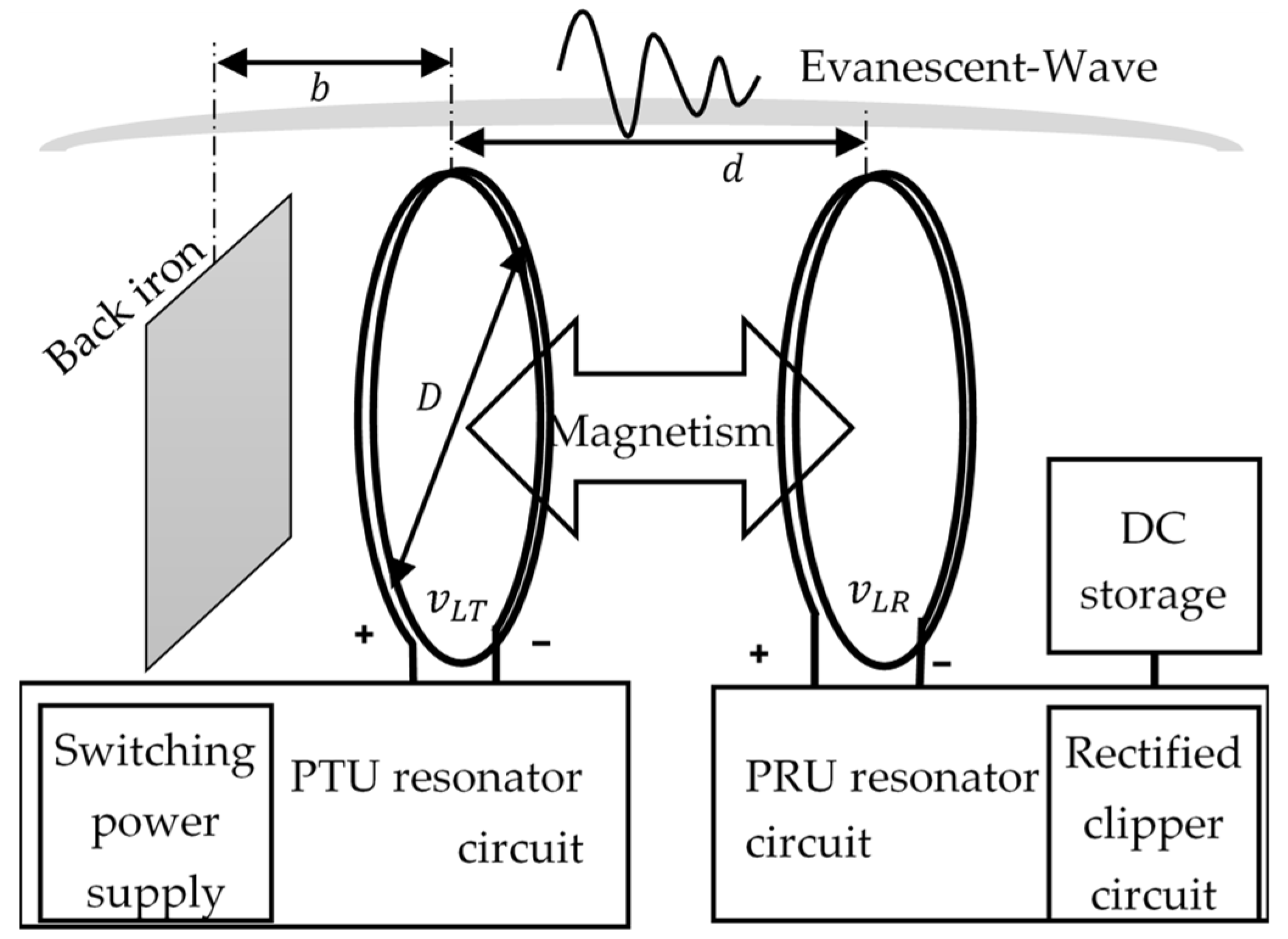
2. GaN HEMT-Based Class-E Resonant Wireless Power Transfer
- Tuning the adjustable capacitor to make the ratio between two coil voltages and an imaginary number, i.e., .Due to the imaginary turn ratio, the impedance of the DC storage system is converted into a negative impedance. The equivalent transformer circuit, which includes this negative impedance, exhibits free oscillation or even a negative damping effect. As a result, the oscillating current increases when the DC storage system is connected to the PRU resonator circuit, thereby maximizing power transfer.
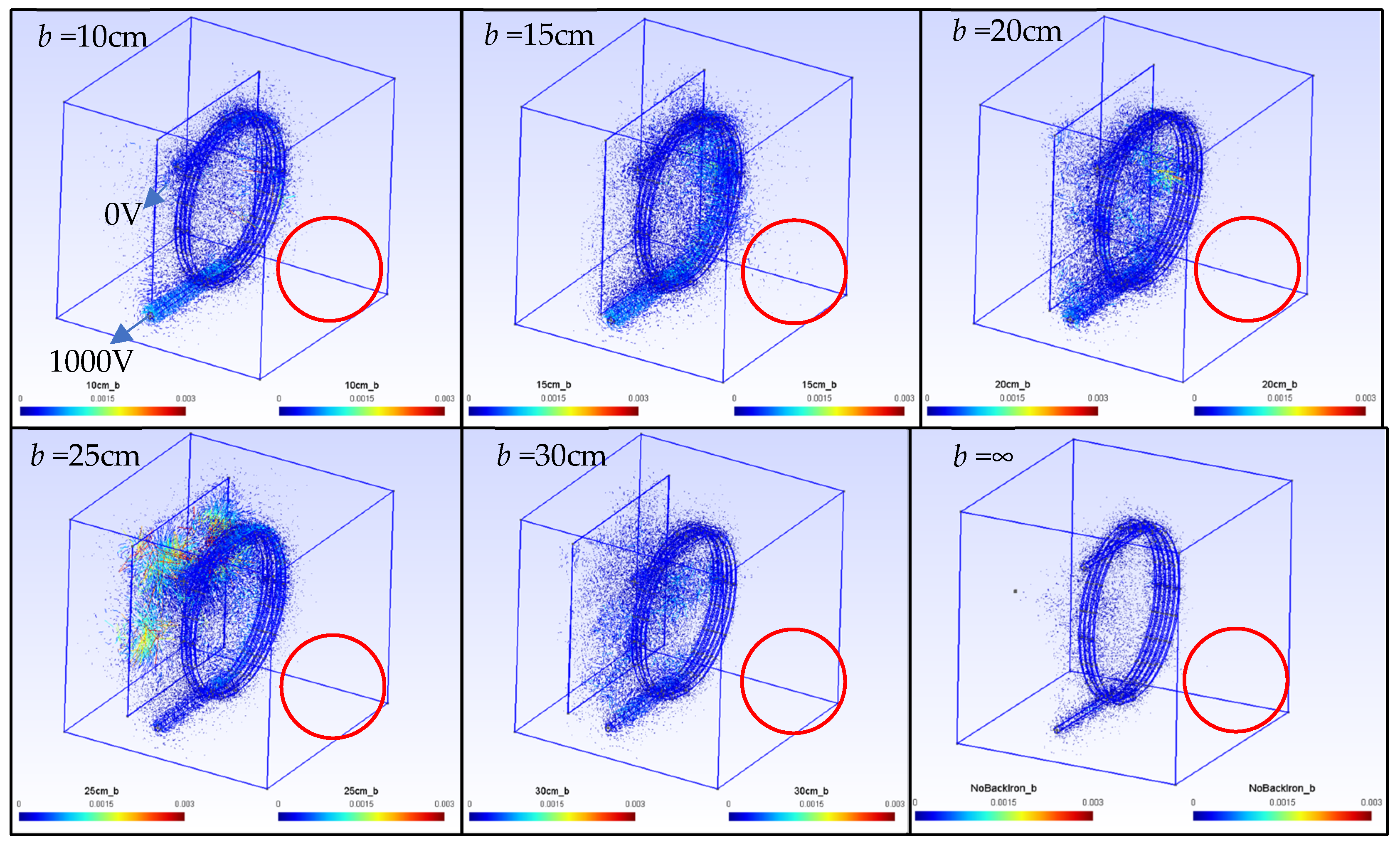
- The back iron distance should be adjusted to balance both high PTE and high PDL.
- The switching frequency and duty cycle of the switching power supply must be controlled to maximize the PTE.
Open Circuit and Short Circuit Test of the PTU Resonator
3. Mathematical Modeling of Resonant Wireless Power Transfer
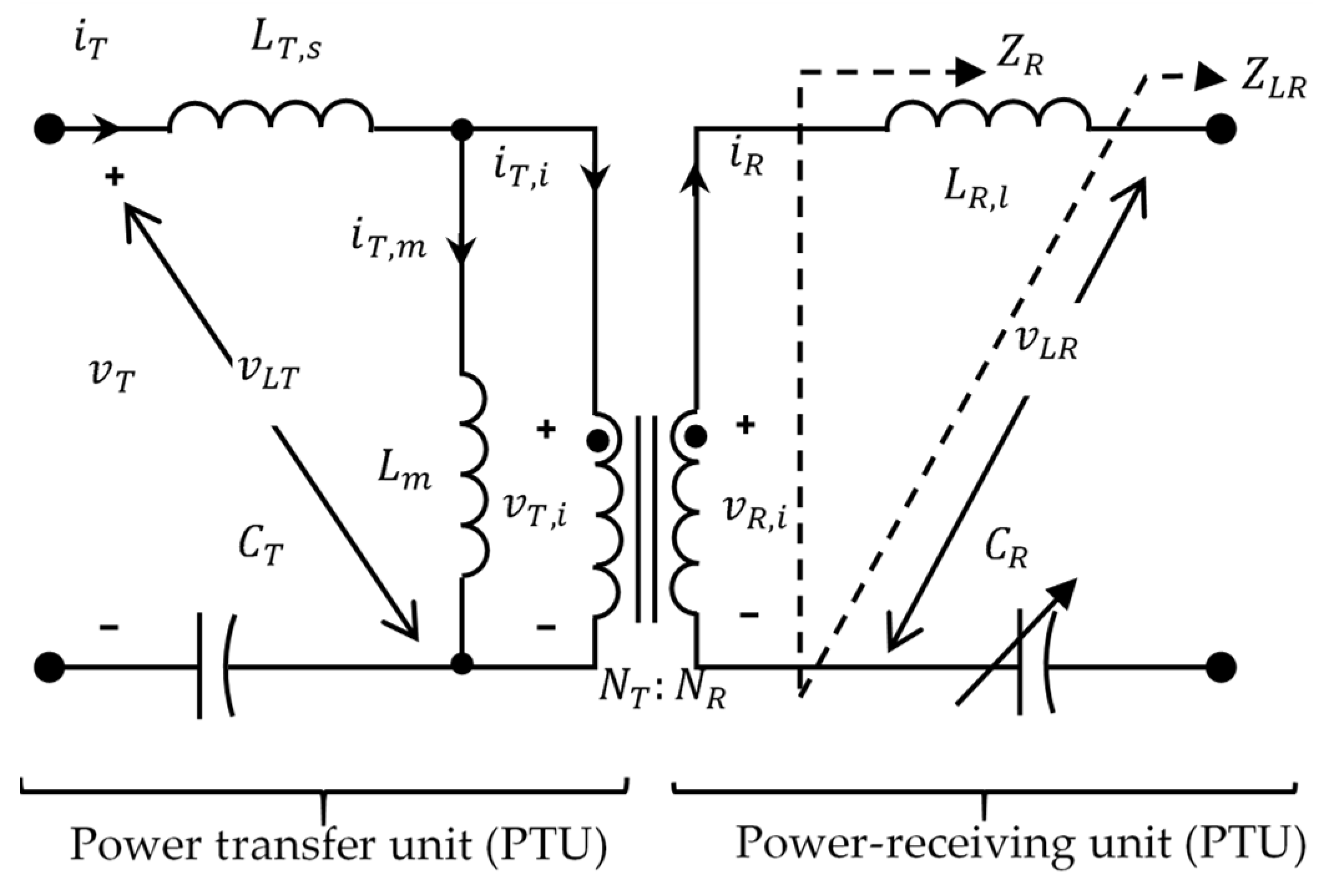
3.1. Imaginary Turn Ratio Conditions
- (1)
- The switching frequency matches the resonant frequency of the PTU’s LC tank, i.e.,
- (2)
- The adjustable capacitor shall set the resonant frequency in the PRU to match the resonant frequency of the PTU’s LC tank, i.e.,
- (3)
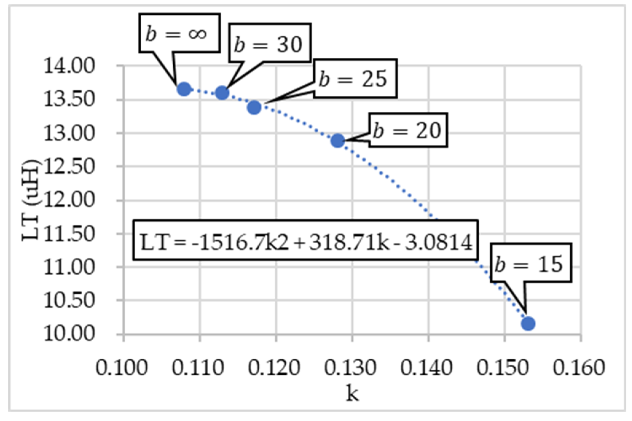
- The back iron shall be placed at a distance to yield the condition that
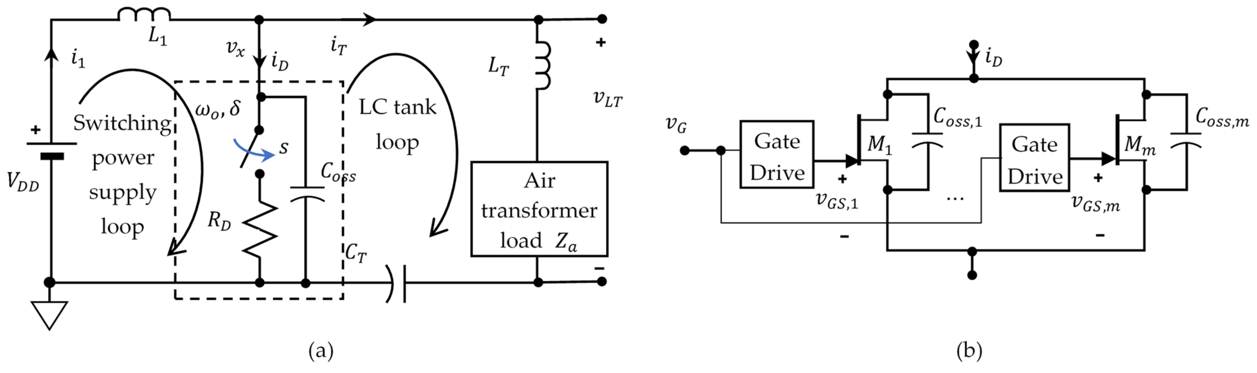
3.2. PTU Resonator with Class-E Amplifier Using Parallel GaN HEMT
3.3. D-Mode GaN HEMT Characteristics
3.4. PRU Resonator with Rectified Clipper Circuit
- Tuning Capacitor : This capacitor is adjusted to achieve the imaginary turn ratio condition indicated in (18).
- Rectified capacitive voltage divider: This consists of two voltage-divider capacitors, and and two bypass diodes, and , which subdivide the resonant voltage. Using the bypass diodes, the capacitor voltages of and are rectified into unipolar voltages.
- Diode-clipping circuit: This circuit consists of a diode and a second-order low-pass LC filter, which transfers the energy from and when their voltage reaches their peaks.
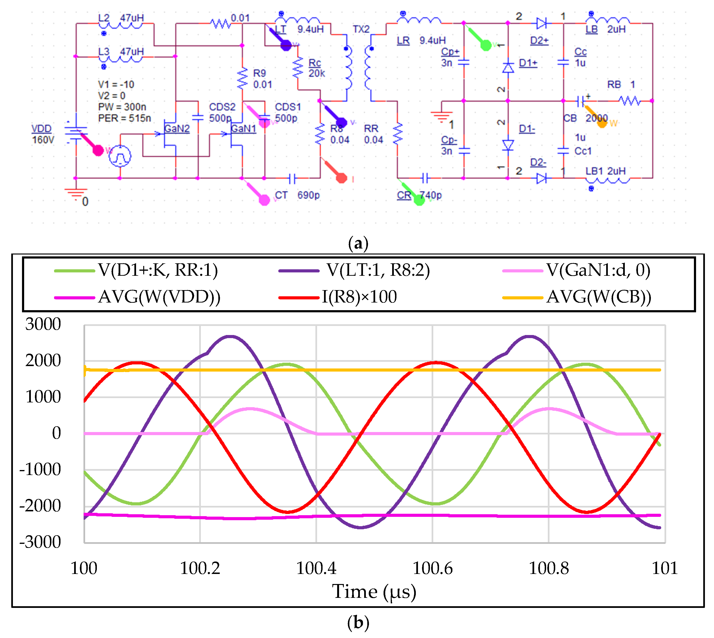
4. Circuit Simulation and Experiments
4.1. Simulation
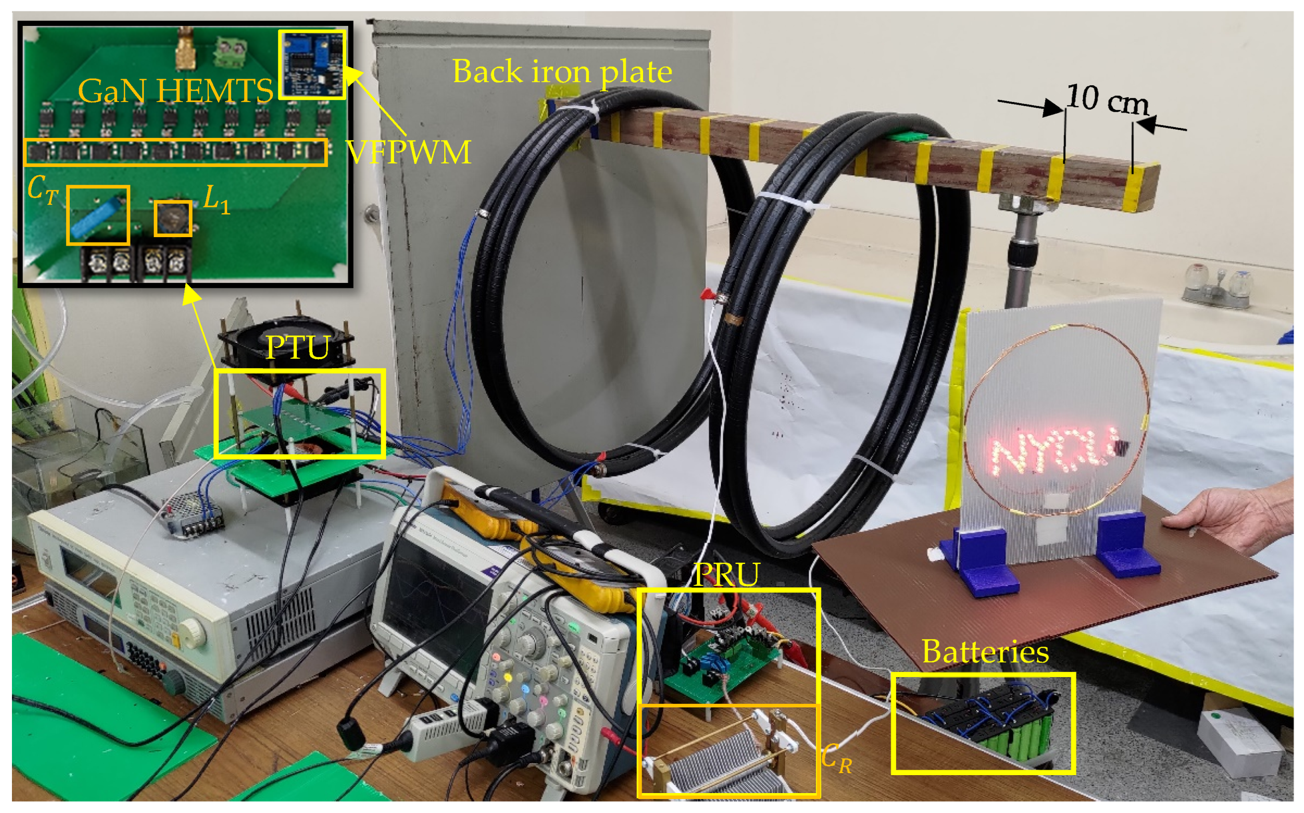
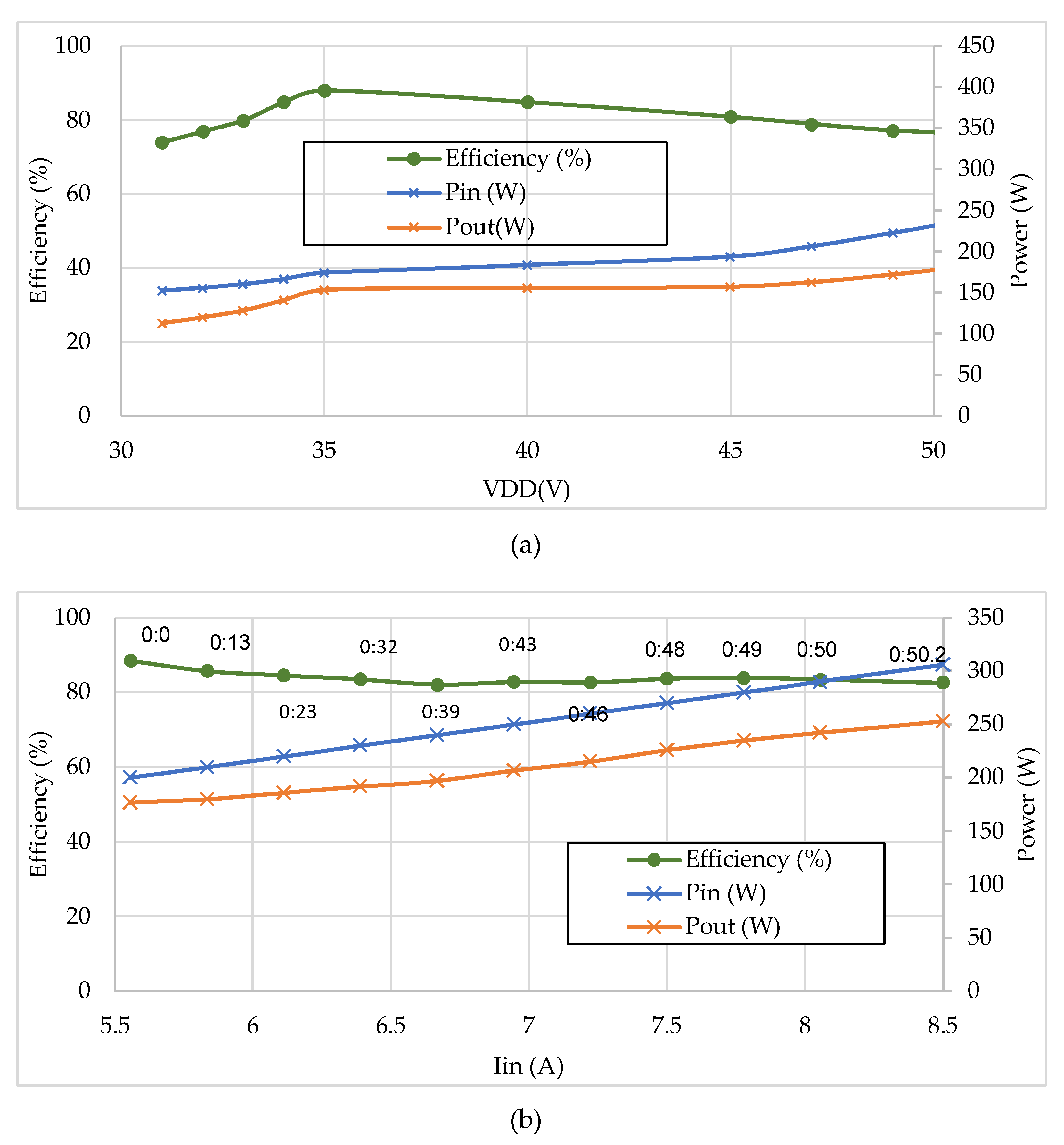
4.2. Experiment
4.3. Power Loss Analysis
5. Discussion
- (1)
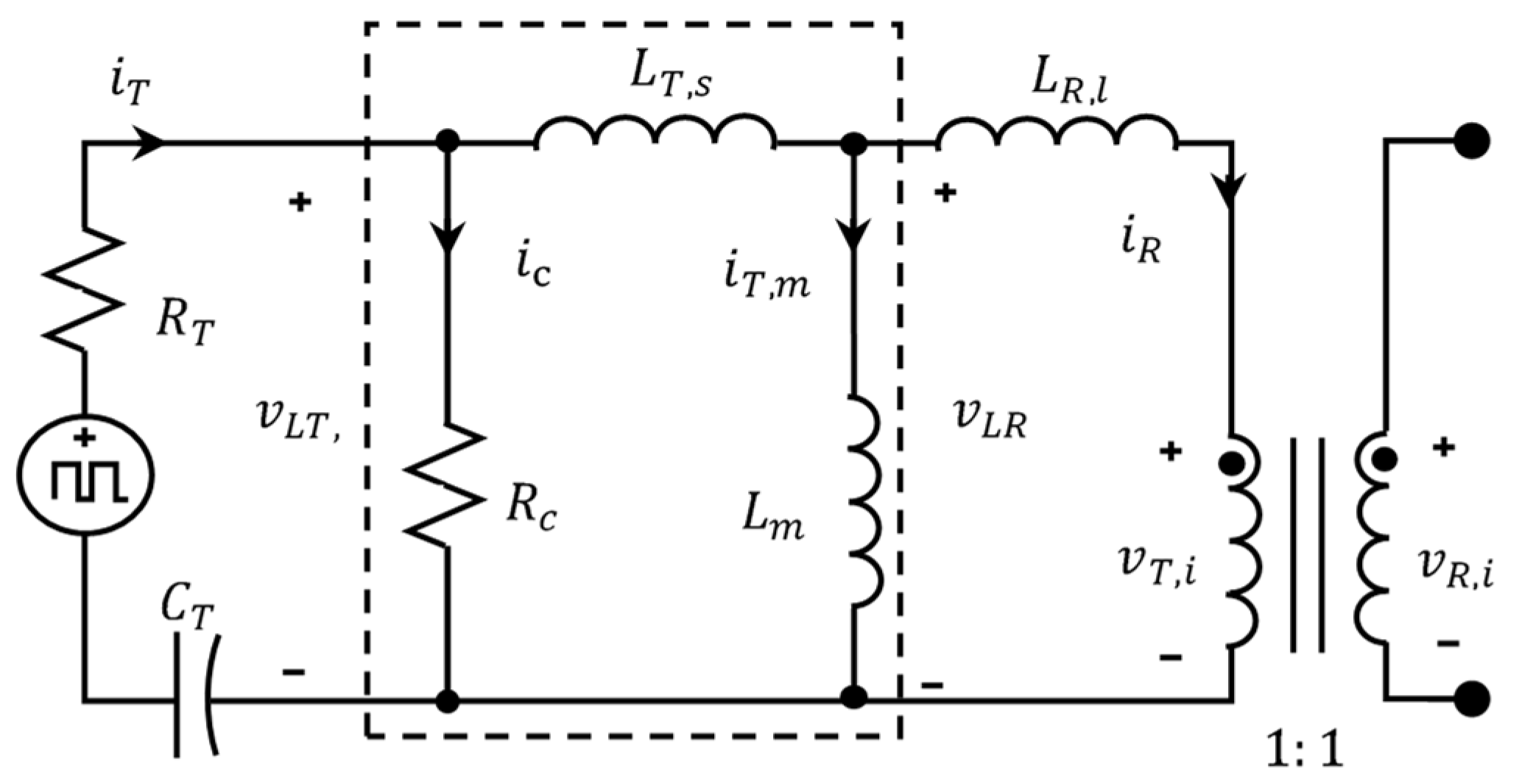
- The Steinmetz model of a transformer was modified for an air-core transformer. The core loss resistor was moved from the magnetization branch to the input port of the air transformer. Therefore, the core loss was not directly associated with the magnetization current; instead, the core loss was associated with the input sinusoidal voltage. Therefore, the loss from the evanescent wave, a function of both the E-field and H-field, can also be included in account of the core loss.
- (2)
- Open circuit and short circuit tests were conducted to experimentally estimate the core loss resistance in the modified Steinmetz model. The back iron can also be a waveguide to guide the electromagnetic wave propagating in the direction of the PRU.
- (3)
- Correlating the resonant quality factor with the coupling coefficient can introduce an “imaginary turn ratio”, which brings the RWPT to a very low damping ratio in the equivalent circuit. When the voltage presented on two sides of the air transformer has a 90-degree phase shift, the positive load resistance on the PRU side is converted into a negative resistance, i.e., the square of the imaginary turn ratio is negative, and moves into its equivalent circuit.
- (4)
- The rectification circuit on the PRU must not interfere with resonance. Therefore, the charges on the PRU side were conveyed to the battery only during the period of time when the capacitor was fully charged.
6. Conclusions
Author Contributions
Funding
Institutional Review Board Statement
Informed Consent Statement
Data Availability Statement
Acknowledgments
Conflicts of Interest
References
- Laha, A.; Kalathy, A.; Pahlevani, M.; Jain, P. A comprehensive review on Wireless Power Transfer Systems for charging portable electronics. Eng 2023, 4, 1023–1057. [Google Scholar] [CrossRef]
- Iqbal, A.; Sura, P.R.; Al-Hasan, M.; Mabrouk, I.B.; Denidni, T.A. Wireless Power Transfer System for deep-implanted biomedical devices. Sci. Rep. 2022, 12, 13689. [Google Scholar] [CrossRef]
- Pahlavan, S.; Shooshtari, M.; Ashtiani, S.J. Star-shaped coils in the transmitter array for receiver rotation tolerance in free-moving wireless power transfer applications. Energies 2022, 15, 8643. [Google Scholar] [CrossRef]
- Pahlavan, S.; Jafarabadi-Ashtiani, S.; Mirbozorgi, S.A. Maze-based Scalable Wireless Power Transmission Experimental Arena for freely moving small animals applications. IEEE Trans. Biomed. Circuits Syst. 2025, 19, 120–129. [Google Scholar] [CrossRef]
- Rahman, M.; Rahman, F.; Rasheduzzaman, A.H.M.; Shahriyar, M.F.; Tanseer Ali, M. Magnetic resonance coupled wireless power transfer analysis for electric vehicle. In Proceedings of the 2021 3rd Global Power, Energy and Communication Conference (GPECOM), Antalya, Turkey, 5–8 October 2021; pp. 28–33. [Google Scholar]
- Ojha, T.; Raptis, T.P.; Passarella, A.; Conti, M. Wireless Power Transfer with unmanned aerial vehicles: State of the art and open challenges. Pervasive Mob. Comput. 2023, 93, 101820. [Google Scholar] [CrossRef]
- Musavi, F.; Edington, M.; Eberle, W. Wireless power transfer: A survey of EV battery charging technologies. In Proceedings of the 2012 IEEE Energy Conversion Congress and Exposition (ECCE), Raleigh, NC, USA, 15–20 September 2012; pp. 804–1810. [Google Scholar]
- Detka, K.; Górecki, K. Wireless Power Transfer—A review. Energies 2022, 15, 7236. [Google Scholar] [CrossRef]
- Villa, J.L.; Sanz, J.; Sallan, J. Inductive battery charging system for electric vehicles. In Proceedings of the 2013 World Electric Vehicle Symposium and Exhibition (EVS27), Barcelona, Spain, 17–20 November 2013; pp. 1–4. [Google Scholar]
- SAE J2954; Wireless charging of plug-in vehicle and positioning Communication. SAE International: Warrendale, PA, USA, 2012.
- Wang, C.-S.; Stielau, O.H.; Covic, G.A. Design considerations for a contactless electric vehicle battery charger. IEEE Trans. Ind. Electron. 2005, 52, 1308–1314. [Google Scholar] [CrossRef]
- Yang, X.; Li, J.; Ding, Y.; Xu, M.; Zhu, X.-F.; Zhu, J. Observation of transient parity-time symmetry in electronic systems. Phys. Rev. Lett. 2022, 128, 065701. [Google Scholar] [CrossRef]
- Correa, D.C.; Resende, U.C.; Bicalho, F.S. Experiments with a compact wireless power transfer system using strongly coupled magnetic resonance and metamaterials. IEEE Trans. Magn. 2019, 55, 1–4. [Google Scholar] [CrossRef]
- Jiang, C.; Chau, K.T.; Liu, C.; Lee, C.H. An overview of resonant circuits for wireless power transfer. Energies 2017, 10, 894. [Google Scholar] [CrossRef]
- Allamehzadeh, H. Wireless power transfer (WPT) fundamentals with resonant frequency-dependent parameters, energy transfer efficiency, and green technology applications. In Proceedings of the 2021 IEEE 48th Photovoltaic Specialists Conference (PVSC), Fort Lauderdale, FL, USA, 20–25 June 2021; pp. 36–40. [Google Scholar]
- Zhang, Z.; Pang, H.; Georgiadis, A.; Cecati, C. Wireless Power Transfer—An overview. IEEE Trans. Ind. Electron. 2019, 66, 1044–1058. [Google Scholar] [CrossRef]
- Choi, J.; Tsukiyama, D.; Tsuruda, Y.; Davila, J.M. High-frequency, high-power resonant inverter with Egan Fet for wireless power transfer. IEEE Trans. Power Electron. 2018, 33, 1890–1896. [Google Scholar] [CrossRef]
- Cõte, N.; Garraud, N.; Sterna, L.; Périchon, P.; Frassati, F.; Boisseau, S. Gan class E wireless power transfer system: A new design method relying on the advanced modeling of parasitic elements. In Proceedings of the 2023 IEEE 22nd International Conference on Micro and Nanotechnology for Power Generation and Energy Conversion Applications (PowerMEMS), Abu Dhabi, United Arab Emirates, 11–14 December 2023; pp. 30–32. [Google Scholar]
- Liu, C.-Y.; Tang, H.-C.; Shieh, Y.-T.; Wu, C.-C.; Chieng, W.-H.; Chang, E.-Y.; Ueda, D. Power receiving unit for high-power resonant wireless power transfer. Energies 2023, 16, 7856. [Google Scholar] [CrossRef]
- Weng, Y.-C.; Wu, C.-C.; Chang, E.; Chieng, W.-H. Minimum power input control for class-E amplifier using depletion-mode gallium nitride high electron mobility transistor. Energies 2021, 14, 2302. [Google Scholar] [CrossRef]
- Liu, C.-Y.; Wang, G.-B.; Wu, C.-C.; Chang, E.; Cheng, S.; Chieng, W.-H. Derivation of the resonance mechanism for wireless power transfer using class-E amplifier. Energies 2021, 14, 632. [Google Scholar] [CrossRef]
- Ghazizadeh, S.; Ahmed, K.; Seyedmahmoudian, M.; Mekhilef, S.; Chandran, J.; Stojcevski, A. Critical analysis of simulation of misalignment in wireless charging of electric vehicles batteries. Batteries 2023, 9, 106. [Google Scholar] [CrossRef]
- Karalis, A.; Joannopoulos, J.D.; Soljačić, M. Efficient Wireless non-radiative mid-range energy transfer. Ann. Phys. 2008, 323, 34–48. [Google Scholar] [CrossRef]
- Kurs, A.; Karalis, A.; Kesler, M.; Campanella, A.; Hall, K.; Kulikowski, K.; Li, Q.; Soljacic, M. Wireless Energy Transfer Systems. U.S. Patent US8629578B2, 14 January 2014. [Google Scholar]
- Yang, X.; Zhang, Z.; Xu, M.; Li, S.; Zhang, Y.; Zhu, X.-F.; Ouyang, X.; Alù, A. Digital non-foster-inspired electronics for broadband impedance matching. Nat. Commun. 2024, 15, 4346. [Google Scholar] [CrossRef]
- Sparselizard—The User Friendly Finite Element c++ Library. Available online: https://www.sparselizard.org/ (accessed on 28 January 2025).
- Geuzaine, C.; Remacle, J. Gmsh: A 3-D finite element mesh generator with built-in pre- and post-processing facilities. Int. J. Numer. Methods Eng. 2009, 79, 1309–1331. [Google Scholar] [CrossRef]
- WiTricity. Available online: https://witricity.com (accessed on 28 January 2025).
- Bosshard, R.; Kolar, J.W.; Muhlethaler, J.; Stevanovic, I.; Wunsch, B.; Canales, F. Modeling and η-α-pareto optimization of inductive power transfer coils for electric vehicles. IEEE J. Emerg. Sel. Top. Power Electron. 2015, 3, 50–64. [Google Scholar] [CrossRef]
- Knecht, O.; Bosshard, R.; Kolar, J.W. High-efficiency transcutaneous energy transfer for implantable mechanical heart support systems. IEEE Trans. Power Electron. 2015, 30, 6221–6236. [Google Scholar] [CrossRef]
- Gu, L.; Zulauf, G.; Stein, A.; Kyaw, P.A.; Chen, T.; Davila, J.M. 6.78-MHz wireless power transfer with self-resonant coils at 95% DC–DC Efficiency. IEEE Trans. Power Electron. 2021, 36, 2456–2460. [Google Scholar] [CrossRef]
- Liu, M.; Fu, M.; Ma, C. Parameter design for a 6.78-MHz wireless power transfer system based on analytical derivation of class E current-driven rectifier. IEEE Trans. Power Electron. 2016, 31, 4280–4291. [Google Scholar] [CrossRef]
- Li, J.; Costinett, D. Comprehensive design for 6.78 MHz Wireless power transfer systems. In Proceedings of the 2018 IEEE Energy Conversion Congress and Exposition (ECCE), Portland, OR, USA, 23–27 September 2018; pp. 906–913. [Google Scholar]
- Arteaga, J.M.; Aldhaher, S.; Kkelis, G.; Yates, D.C.; Mitcheson, P.D. Multi-MHz IPT systems for Variable Coupling. IEEE Trans. Power Electron. 2018, 33, 7744–7758. [Google Scholar] [CrossRef]
- Gu, L.; Rivas-Davila, J. 1.7 kW 6.78 MHz wireless power transfer with air-core coils at 95.7% DC-DC efficiency. In Proceedings of the 2021 IEEE Wireless Power Transfer Conference (WPTC), San Diego, CA, USA, 1–4 June 2021; pp. 1–4. [Google Scholar]
- Surakitbovorn, K.; Rivas-Davilla, J. Design of a gan-based wireless power transfer system at 13.56 MHz to replace conventional wired connection in a vehicle. In Proceedings of the 2018 International Power Electronics Conference (IPEC-Niigata 2018 -ECCE Asia), Niigata, Japan, 20–24 May 2018; pp. 3848–3854. [Google Scholar]


| Symbol | Description | Unit | Value | |
|---|---|---|---|---|
| Class-E Inductor | μH | 47 | ||
| PTU, PRU Coil Inductance | μH | 10 | ||
| PTU Capacitor | pF | 680 | ||
| Tuning Capacitor | pF | 200~1000 | ||
| PTU/PRU Coil Diameter | cm | 72 | ||
| Voltage-divider Capacitor | nF | 3 | ||
| Low-pass LC Filter Capacitor | μF | 1 | ||
| Low-pass LC Filter Inductor | μH | 2 | ||
| Gate Driver | UCC27614DR | 30 V, 10 A | ||
| STPSC4H065B-TR | 650 V, 4 A | |||
| Battery | NCR18650B | 45s2p, 180 V/6.8 Ah | ||
| GaN HEMT Output Capacitance | pF | |||
| 0 V | 600 V | |||
| 31 | 17 | |||
| GaN HEMT Input Capacitance | pF | 46 | 31 | |
| GaN HEMT Feedback Capacitance | pF | 23 | 8 | |
| GaN HEMT Gate Turn-on Voltage | V | −9 | ||
| GaN HEMT Maximum | V | 10~−30 | ||
| GaN HEMT On-Resistance | m | 900 | ||
| GaN HEMT Breakdown Voltage | V | 600 | ||
| GaN HEMT Continuous Drain Current | A | 3 | ||
| Power Losses | Definition |
|---|---|
| The power loss on the back iron and the surrounding due to the eddy current and evanescent wave effect. | |
| The power loss on a GaN HEMT during the on-state due to transistor on-resistance. | |
| The power loss on a GaN HEMT while ZVS and ZCS is not achieved. | |
| The power loss on the PTU due to , including the coil resistance, the ESR loss of the capacitors, and the resistance on the PCB circuit board during the on-state. The on-resistance of the GaN HEMTs is subtracted from since we already have . |
| Frequency | Type | Coil Gap | PTE | PDL | FOM | |
|---|---|---|---|---|---|---|
| Unit | MHz | mm | % | W | ||
| WiTricity [28] | 0.085 | IWPT | N/A | 93 | 11,000 | N/A |
| R. Bosshard et al. [29] | 0.1 | IWPT | 52 | 97 | 5000 | 2.52 × 10⁷ |
| O. Knecht et al. [30] | 0.8 | IWPT | 20 | 96 | 30 | 5.76 × 10⁴ |
| This study | 2 | RWPT | 500 | 88 | 250 | 1.10 × 10⁷ |
| L. Gu et al. [31] | 6.78 | RWPT | 19 | 95 | 1000 | 1.81 × 10⁶ |
| M. Liu et al. [32] | 6.78 | RWPT | 40 | 84 | 20 | 6.72 × 10⁴ |
| J. Li and D. Costinett [33] | 6.78 | RWPT | N/A | 85 | 10 | N/A |
| J. M. Arteaga et al. [34] | 6.78 | RWPT | 110 | 88 | 50 | 4.84 × 10⁵ |
| L. Gu and J. Rivas-Davila [35] | 6.78 | RWPT | 55 | 96 | 1700 | 8.98 × 10⁶ |
| K. Surakitbovorn and J. Rivas [36] | 13.56 | RWPT | 15 | 90 | 300 | 4.05 × 10⁵ |
Disclaimer/Publisher’s Note: The statements, opinions and data contained in all publications are solely those of the individual author(s) and contributor(s) and not of MDPI and/or the editor(s). MDPI and/or the editor(s) disclaim responsibility for any injury to people or property resulting from any ideas, methods, instructions or products referred to in the content. |
© 2025 by the authors. Licensee MDPI, Basel, Switzerland. This article is an open access article distributed under the terms and conditions of the Creative Commons Attribution (CC BY) license (https://creativecommons.org/licenses/by/4.0/).
Share and Cite
Tang, H.-C.; Chen, C.-H.; Chang, E.-Y.; Yao, D.-J.; Chieng, W.-H.; He, J.-Y. A Long-Range, High-Efficiency Resonant Wireless Power Transfer via Imaginary Turn Ratio Air Voltage Transformer. Energies 2025, 18, 1329. https://doi.org/10.3390/en18061329
Tang H-C, Chen C-H, Chang E-Y, Yao D-J, Chieng W-H, He J-Y. A Long-Range, High-Efficiency Resonant Wireless Power Transfer via Imaginary Turn Ratio Air Voltage Transformer. Energies. 2025; 18(6):1329. https://doi.org/10.3390/en18061329
Chicago/Turabian StyleTang, Hsien-Chung, Chun-Hao Chen, Edward-Yi Chang, Da-Jeng Yao, Wei-Hua Chieng, and Jun-Ying He. 2025. "A Long-Range, High-Efficiency Resonant Wireless Power Transfer via Imaginary Turn Ratio Air Voltage Transformer" Energies 18, no. 6: 1329. https://doi.org/10.3390/en18061329
APA StyleTang, H.-C., Chen, C.-H., Chang, E.-Y., Yao, D.-J., Chieng, W.-H., & He, J.-Y. (2025). A Long-Range, High-Efficiency Resonant Wireless Power Transfer via Imaginary Turn Ratio Air Voltage Transformer. Energies, 18(6), 1329. https://doi.org/10.3390/en18061329