
A Modified Nearest Level Control Scheme for Improved Submodule Current Sharing in a CHB Converter with Integrated EDLCs


Abstract
:1. Introduction
2. Materials and Methods
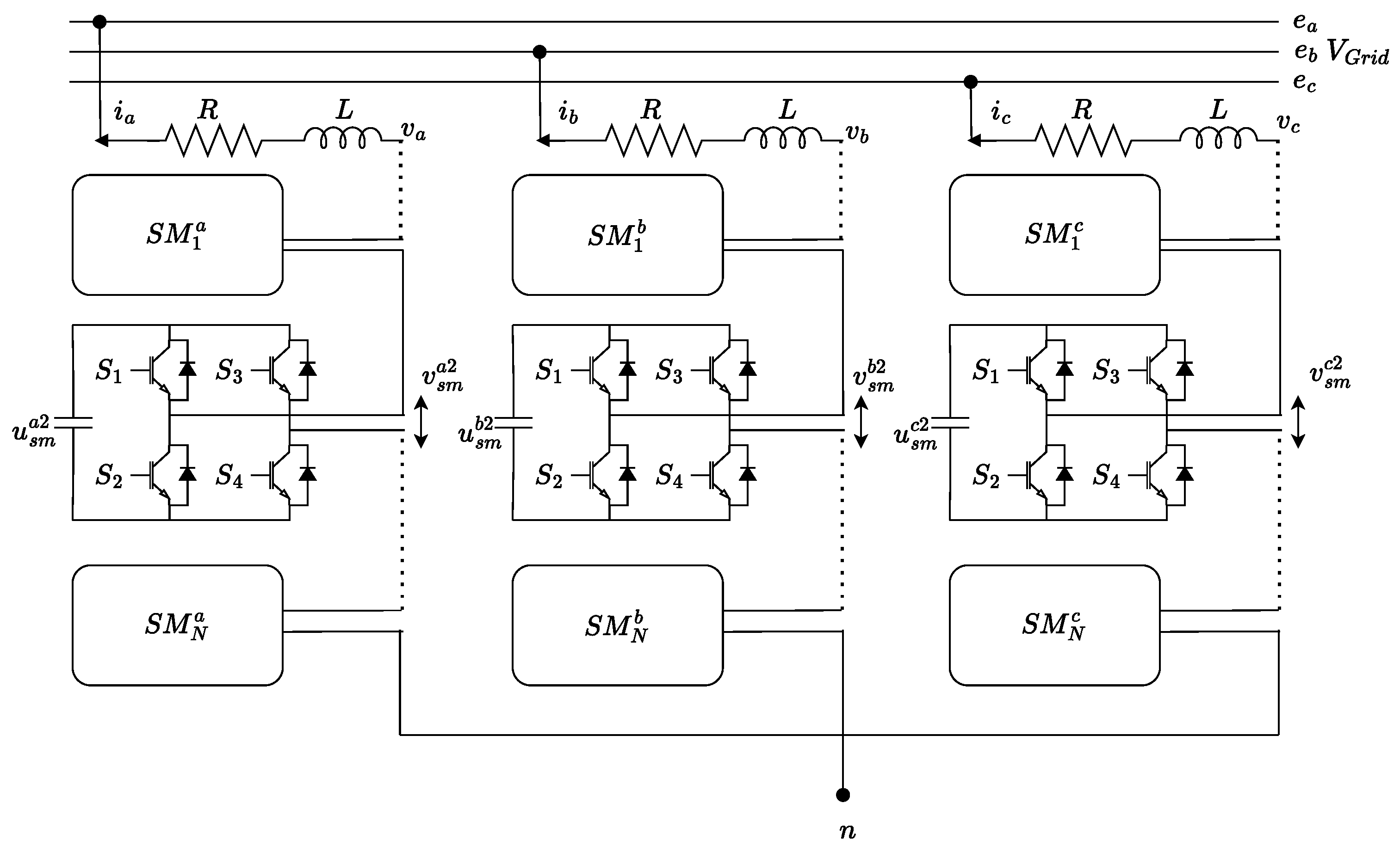
2.1. Converter Outline and General Assumptions
2.2. Voltage and Current Limitations
2.2.1. Voltage Limitations
2.2.2. Current Limitations
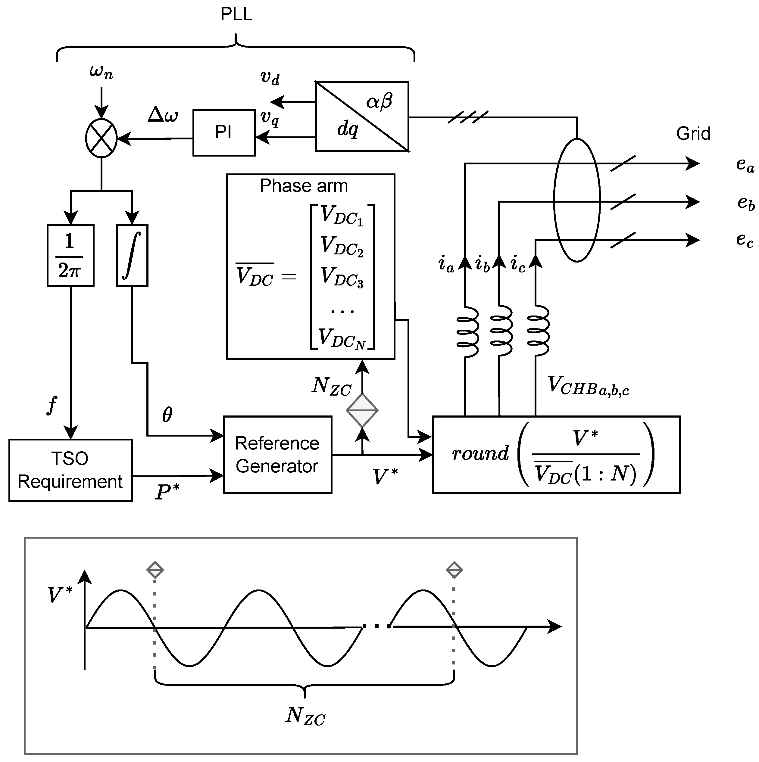
2.3. Conventional Nearest Level Modulation with Voltage Balancing
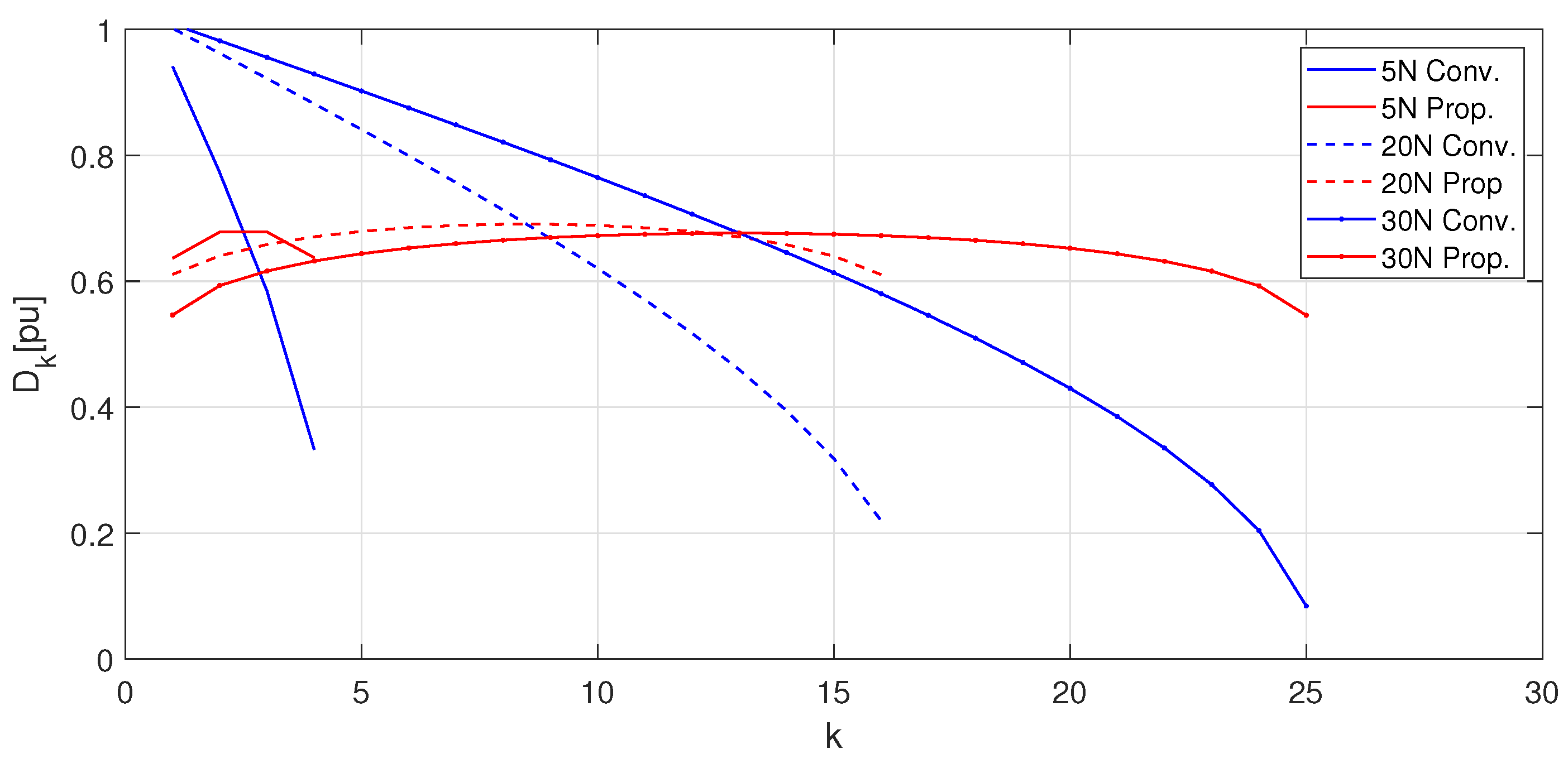
Duty Cycle in Conventional NLM
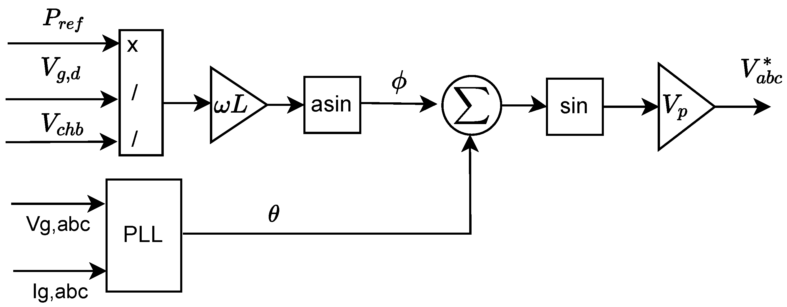
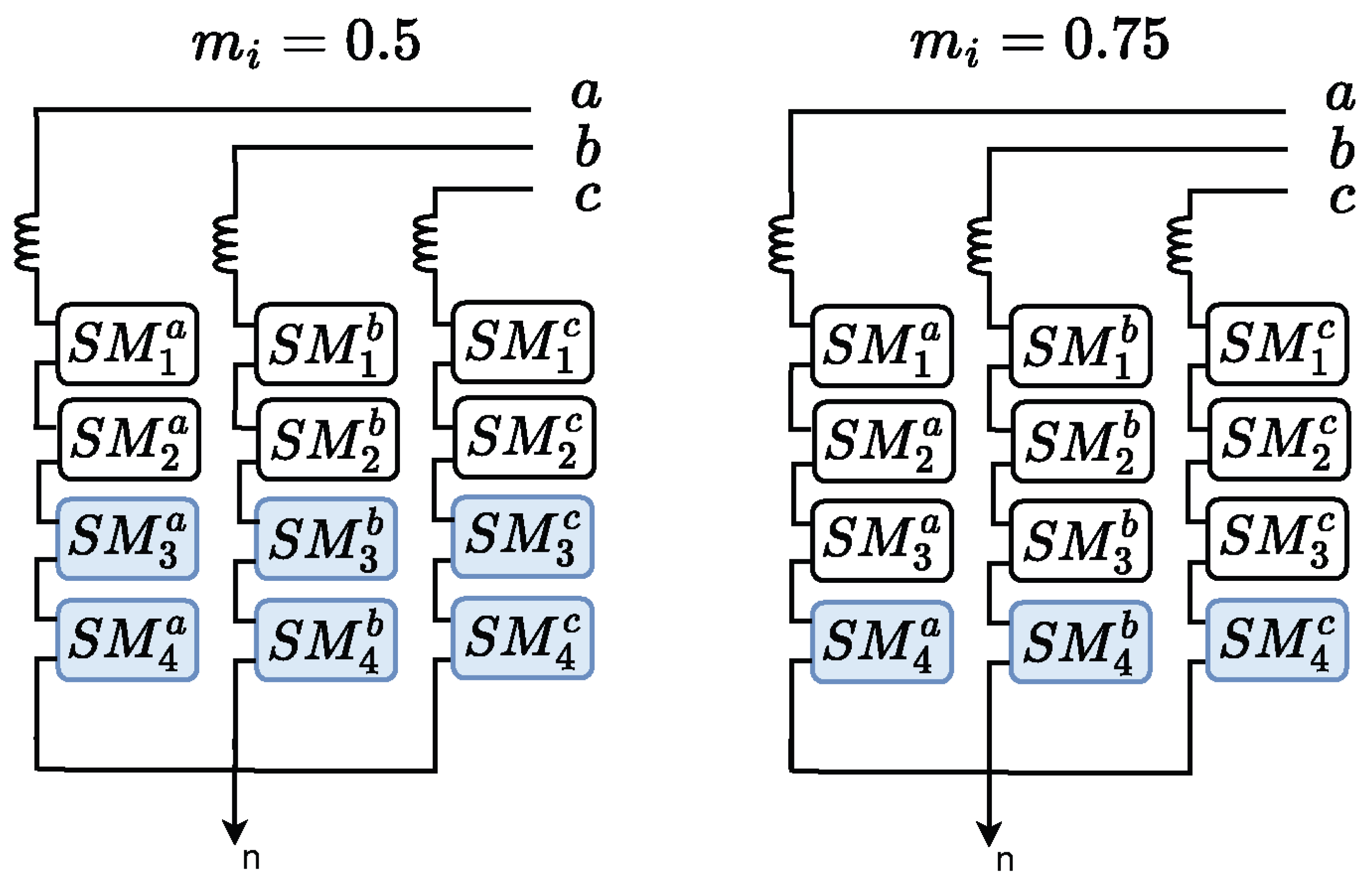
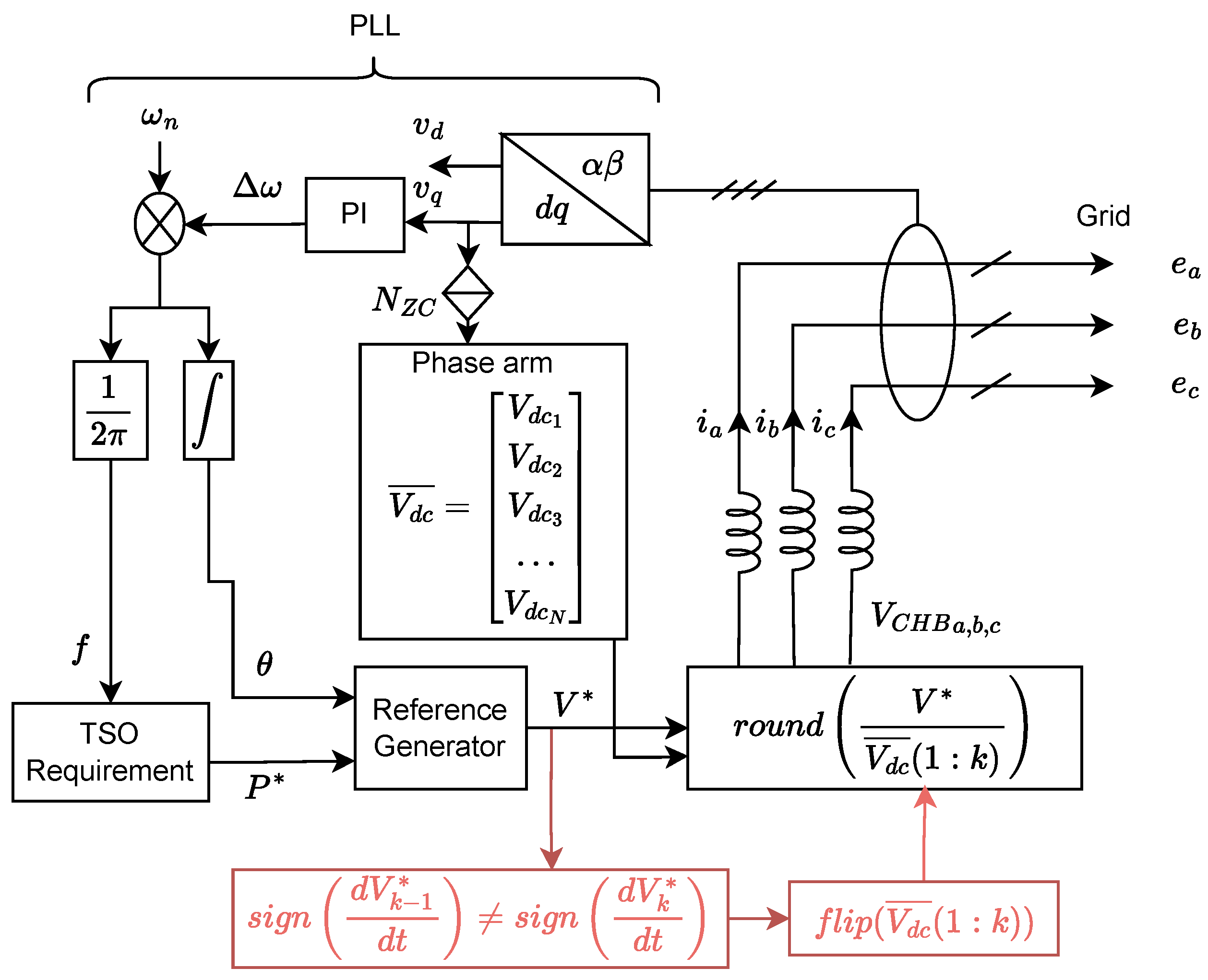
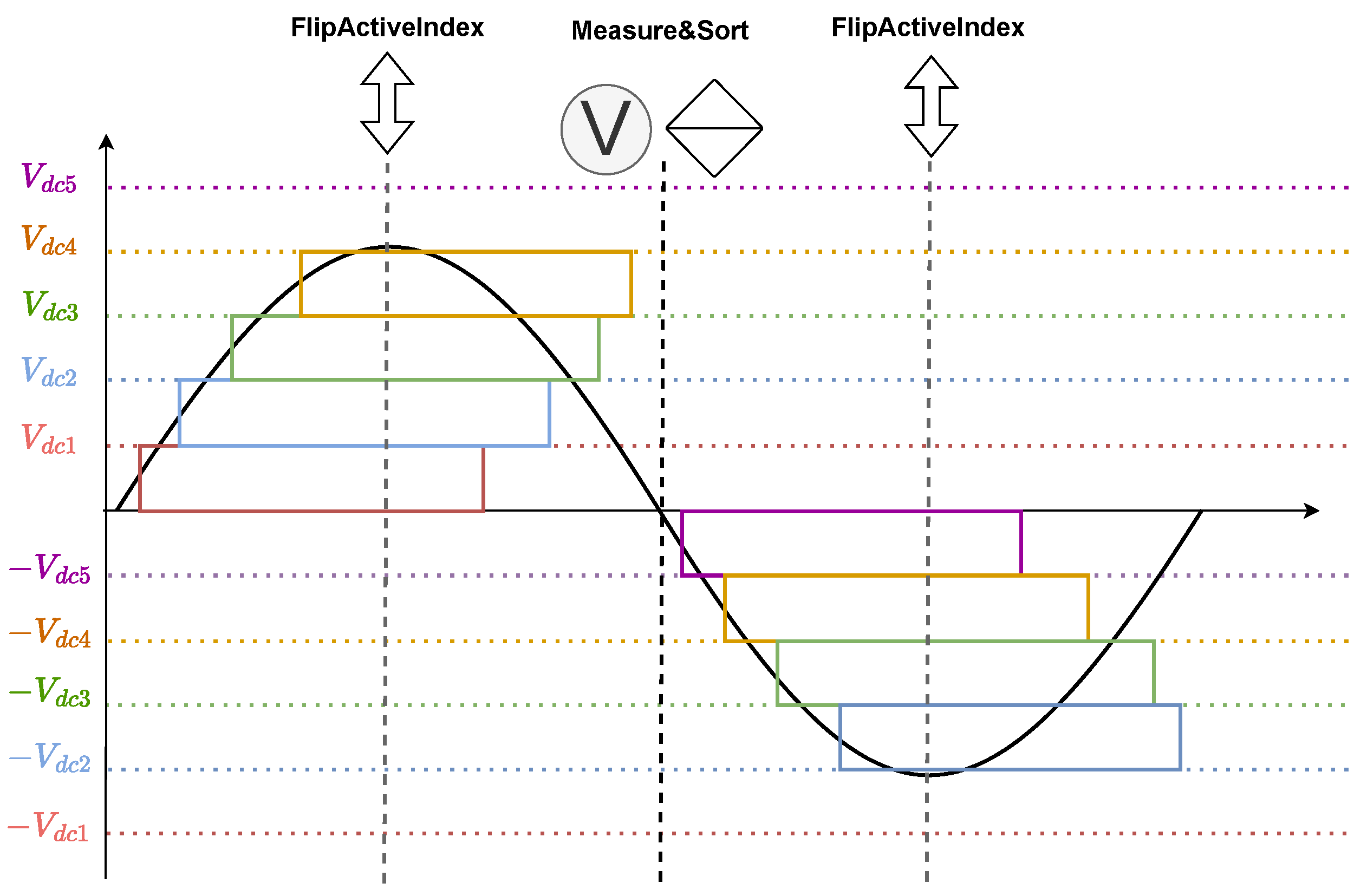
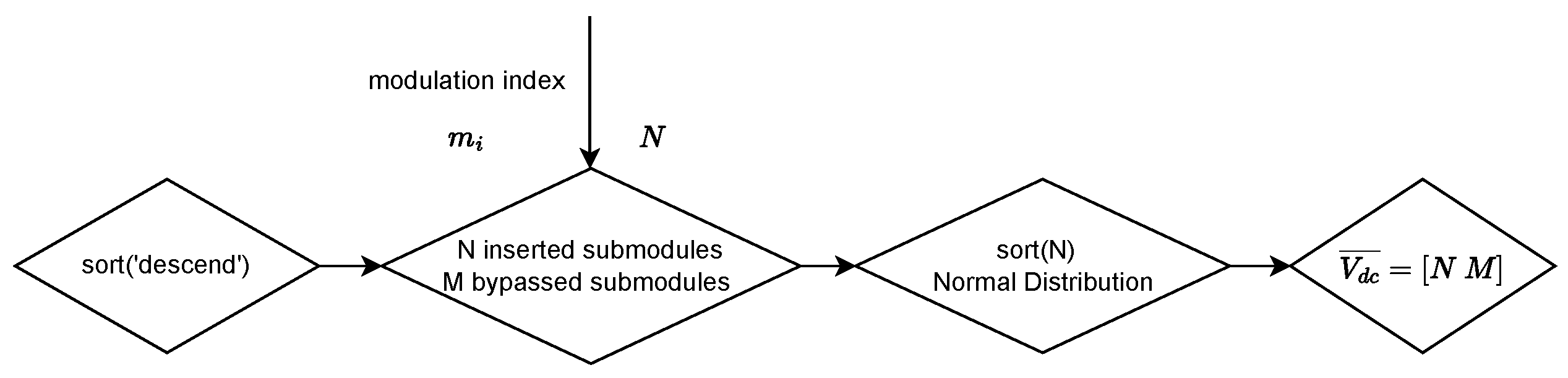
2.4. Modified Nearest Level Modulation Algorithm
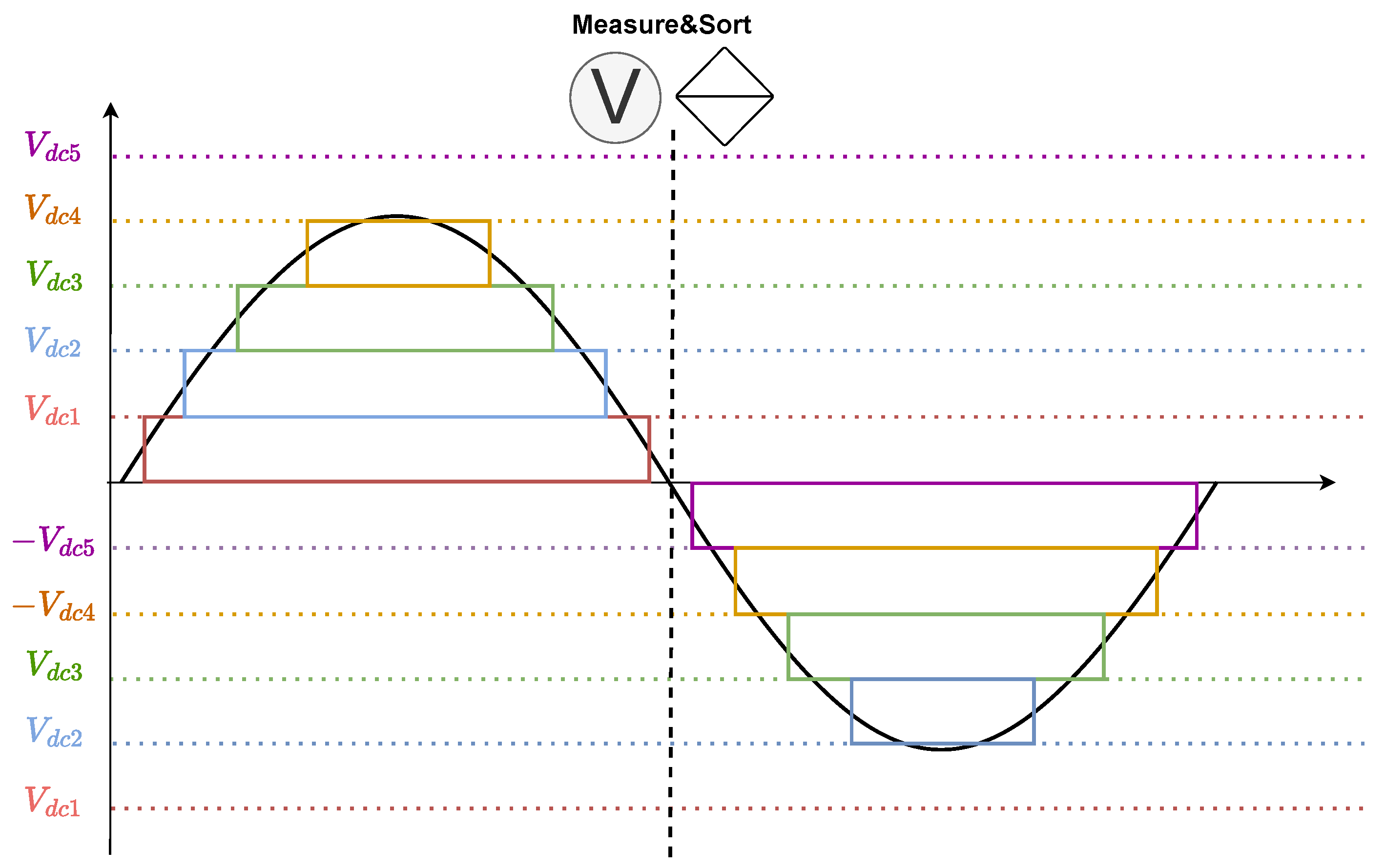
2.5. Sorting and Vertical Voltage Balance
2.6. Simulations
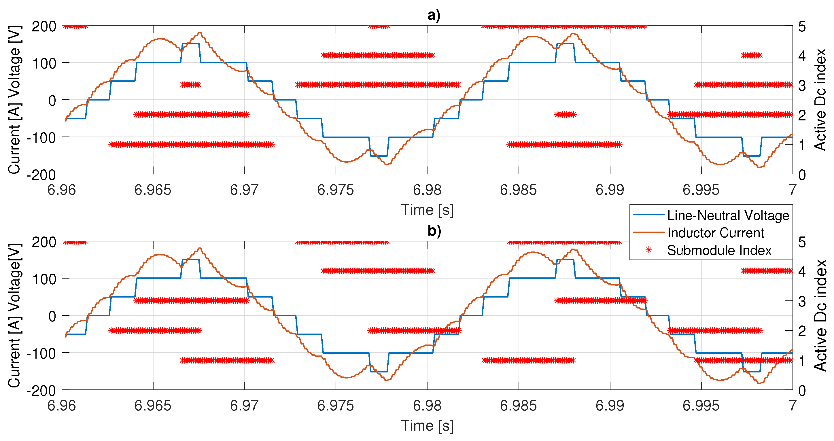
3. Results
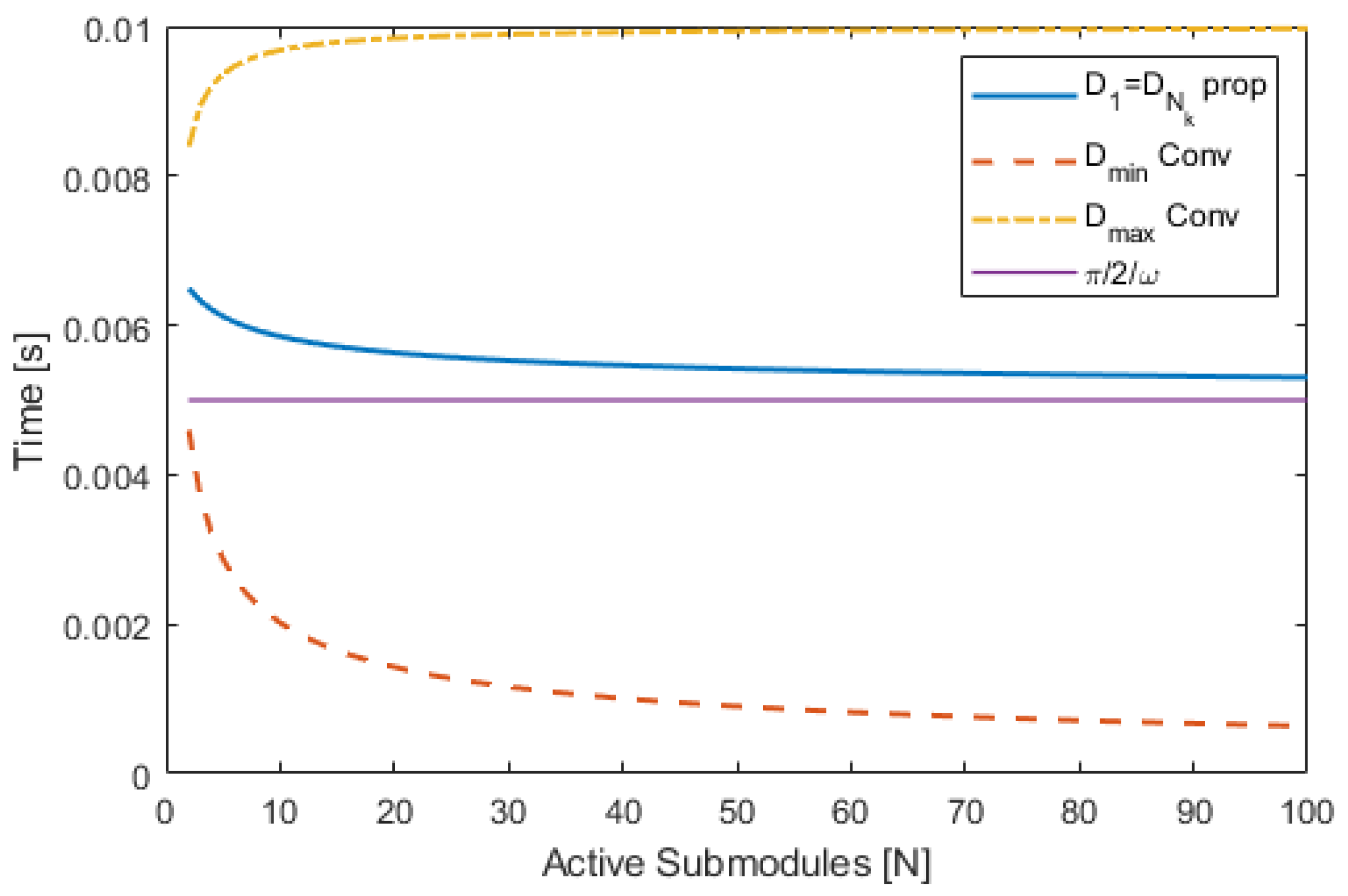
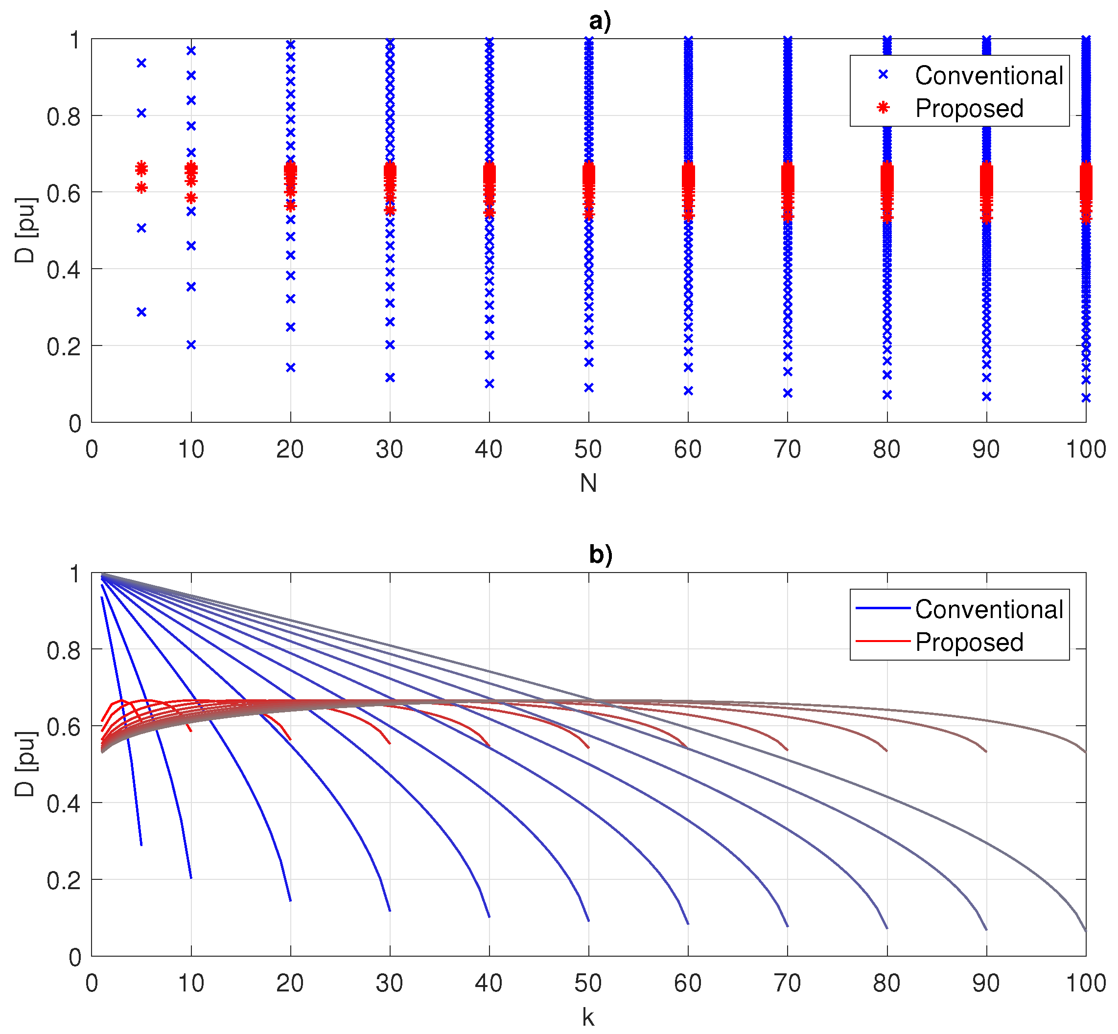
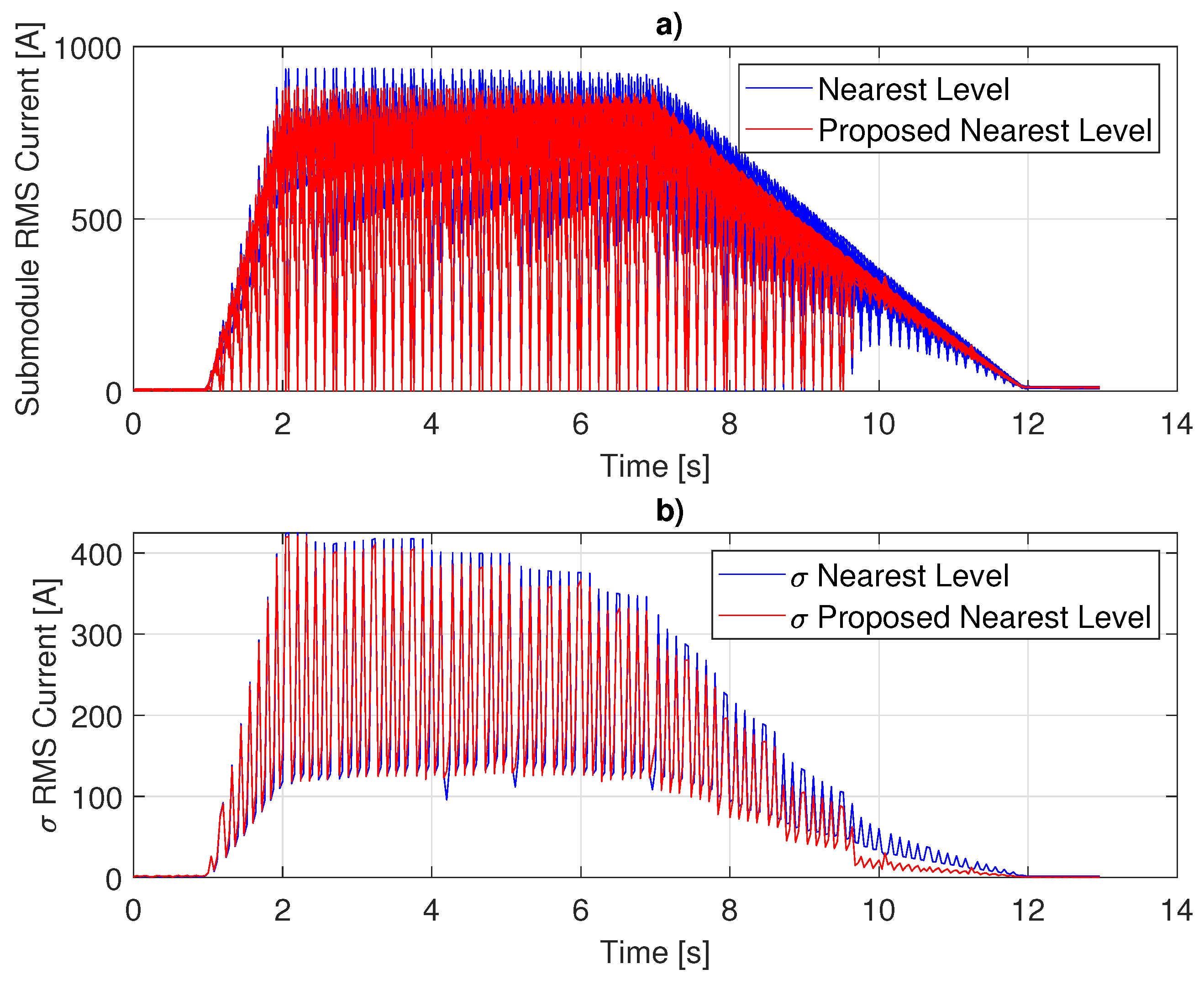
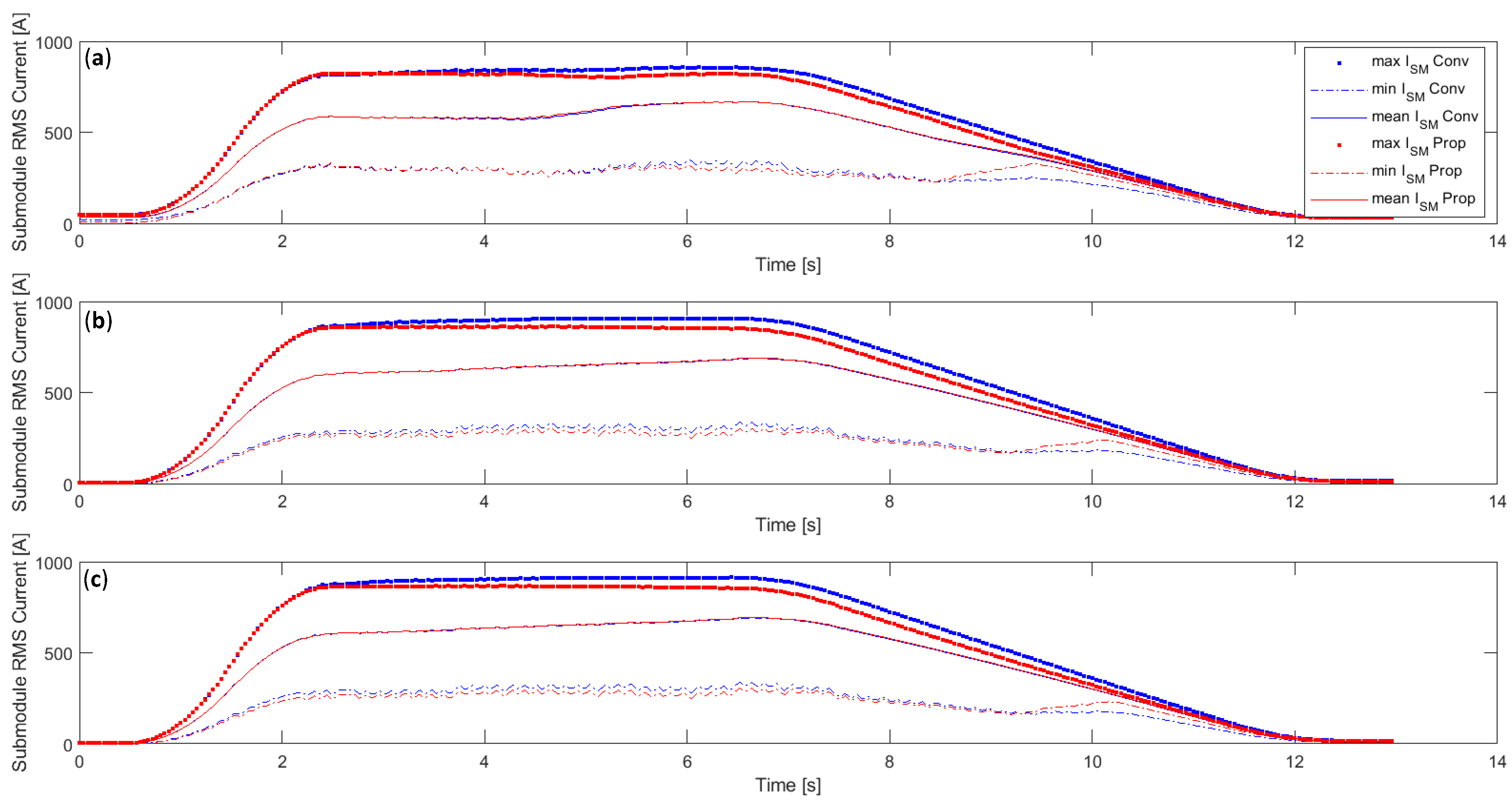
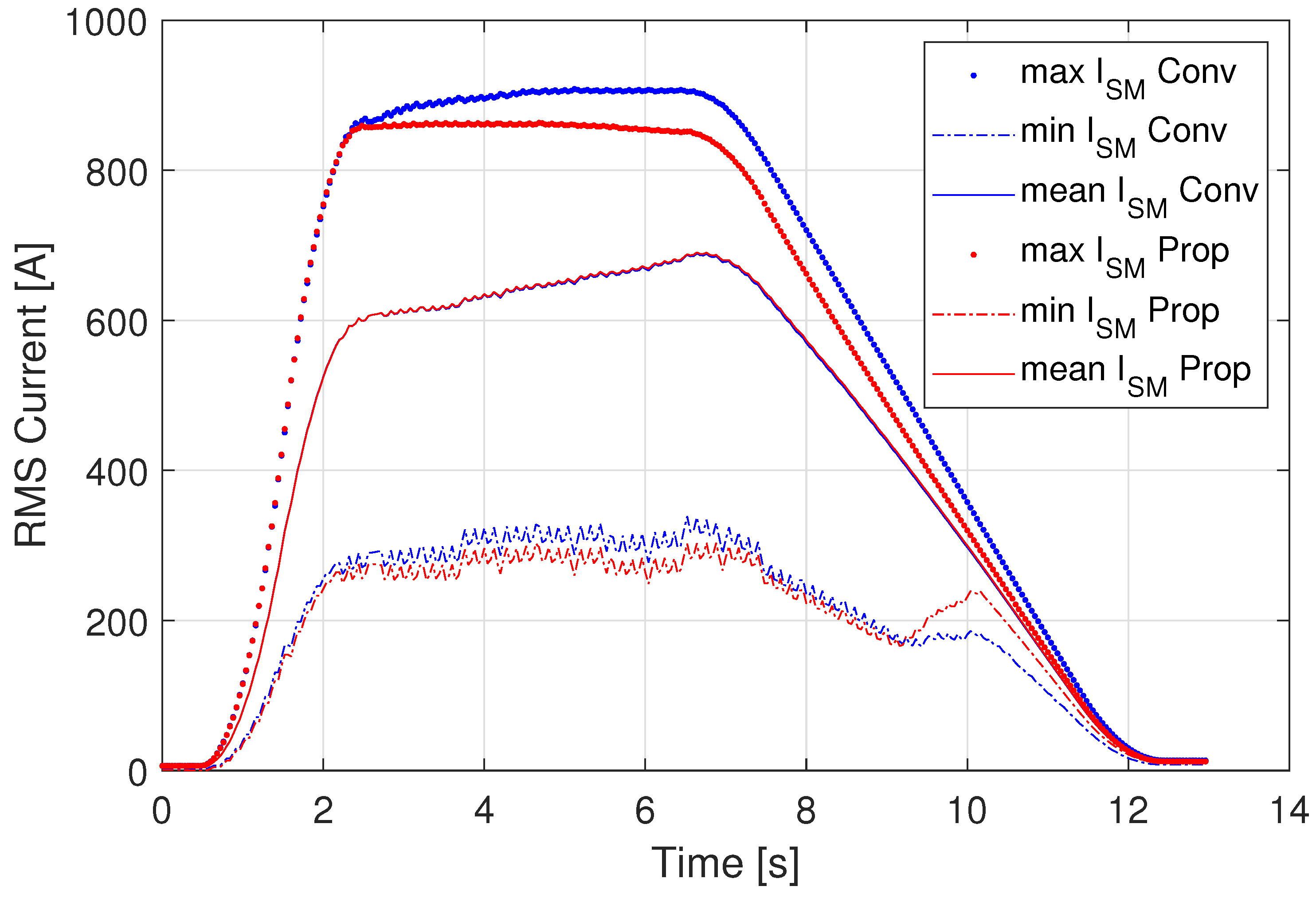
3.1. Distribution of RMS Current
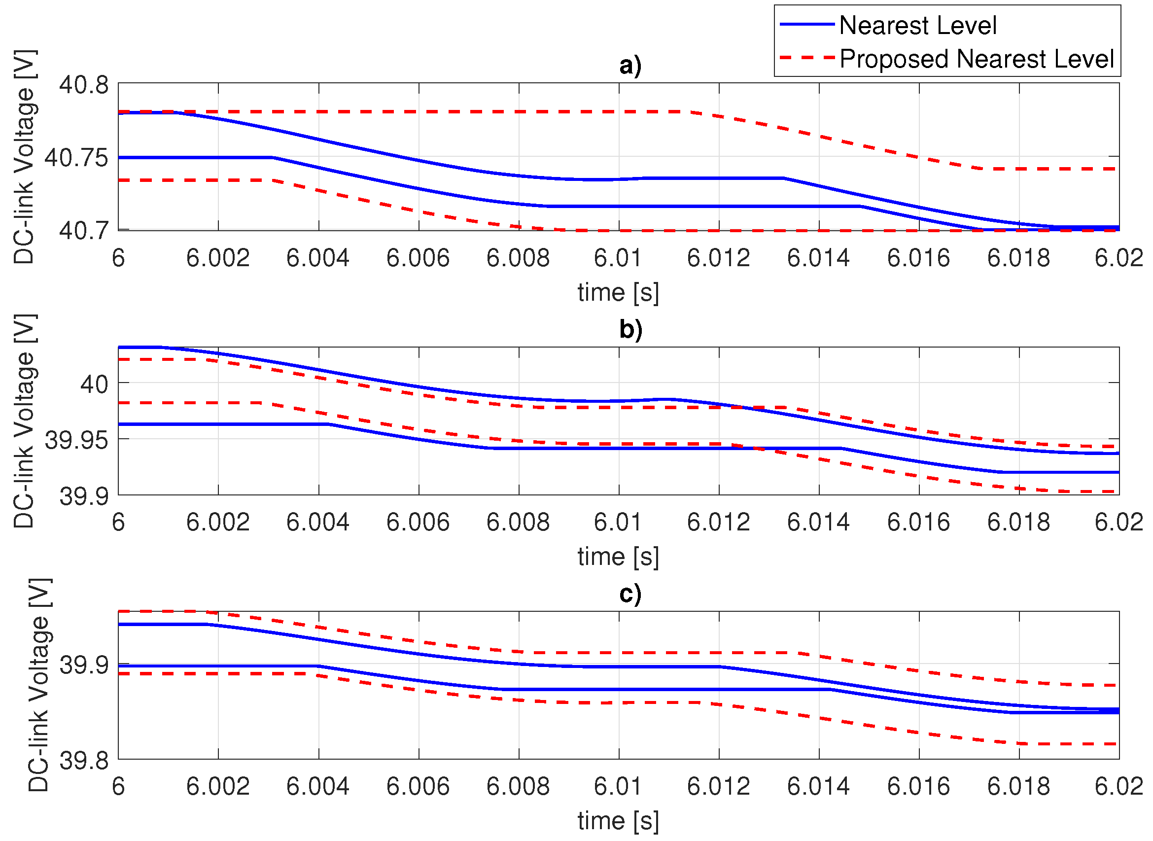
3.2. Vertical Voltage Balancing
4. Discussion
5. Conclusions
Author Contributions
Funding
Data Availability Statement
Conflicts of Interest
Abbreviations
| NLM | Nearest Level Modulation |
| CHB | Cascaded H-Bridge |
| RMS | Root Mean Square |
| EDLC | Electric Double Layer Capacitor |
| TSO | Transmission System Operator |
References
- Kim, J.; Gevorgian, V.; Luo, Y.; Mohanpurkar, M.; Koritarov, V.; Hovsapian, R.; Member, S.; Muljadi, E.; Kim Kim, J.J.; Muljadi, E.; et al. Supercapacitor to Provide Ancillary Services with Control Coordination. IEEE Trans. Ind. Appl. 2019, 55, 5119. [Google Scholar] [CrossRef]
- Döhlen, V.; Bertilsson, K. Direct integration of supercapacitors in CHB converter with low voltage components for Fast Frequency Reserve and enhanced response from Kaplan turbines. In Proceedings of the 4th International Conference on Electrical, Control and Instrumentation Engineering (ICECIE), Kuala Lumpur, Malaysia, 26 November 2022; Volume 2022, pp. 1–8. [Google Scholar] [CrossRef]
- Singh, V.K.; Banerjee, A.; Shafiul Alam, S.M.; Mosier, T.M. Dynamic Frequency Regulation Improvement in Hydropower-Hybrid System using Variational Mode Decomposition. In Proceedings of the 2022 IEEE/PES Transmission and Distribution Conference and Exposition (T&D), New Orleans, LA, USA, 25–28 April 2022; pp. 1–5. [Google Scholar] [CrossRef]
- Gevorgian, V.; Muljadi, E.; Luo, Y.; Mohanpurkar, M.; Hovsapian, R.; Koritarov, V. Supercapacitor to provide ancillary services. In Proceedings of the 2017 IEEE Energy Conversion Congress and Exposition (ECCE), Cincinnati, OH, USA, 1–5 October 2017; pp. 1030–1036. [Google Scholar] [CrossRef]
- Shafiul Alam, S.M.; Banerjee, A.; Mosier, T.M. Power Hardware-In-the-Loop Hydropower and Ultracapacitor Hybrid Testbed. In Proceedings of the 2022 IEEE Power & Energy Society General Meeting (PESGM), Denver, CO, USA, 17–21 July 2022; pp. 1–5. [Google Scholar] [CrossRef]
- Maharjan, L.; Inoue, S.; Akagi, H. A Transformerless Energy Storage System Based on a Cascade Multilevel PWM Converter with Star Configuration. IEEE Trans. Ind. Appl. 2008, 44, 1621–1630. [Google Scholar] [CrossRef]
- Baruschka, L.; Mertens, A. Comparison of Cascaded H-Bridge and Modular Multilevel Converters for BESS application. In Proceedings of the 2011 IEEE Energy Conversion Congress and Exposition, Phoenix, AZ, USA, 17–22 September 2011. [Google Scholar] [CrossRef]
- Bignucolo, F.; Caldon, R.; Coppo, M.; Pasut, F.; Pettinà, M. Integration of Lithium-Ion Battery Storage Systems in Hydroelectric Plants for Supplying Primary Control Reserve. Energies 2017, 10, 98. [Google Scholar] [CrossRef]
- STATCOM—SVC Light® Enhanced. Hitachi Energy. Available online: https://www.hitachienergy.com/products-and-solutions/facts/statcom/svc-light-enhanced (accessed on 17 September 2024).
- Errigo, F.; Venet, P.; Chédot, L.; Sari, A. Optimal supercapacitor pack sizing for modular multilevel converter with integrated energy storage system. In Proceedings of the 2018 IEEE International Conference on Industrial Technology (ICIT), Lyon, France, 20–22 February 2018; pp. 1760–1766. [Google Scholar] [CrossRef]
- Errigo, F.; Morel, F.; Member, S.; Mathieu De Vienne, C.; Chédot, L.; Sari, A.; Venet, P. A Submodule with Integrated Supercapacitors for HVDC-MMC providing Fast Frequency Response. IEEE Trans. Power Deliv. 2021, 37, 1423–1432. [Google Scholar] [CrossRef]
- Asoodar, M.; Nahalparvari, M.; Bakas, P.; Hasler, J.P.; Meng, L.; Nee, H.P. A Computationally Efficient Model for Large-Scale Energy Storage Systems with Active Voltage Balancing in Modular Multilevel Converters. In Proceedings of the 2023 IEEE Applied Power Electronics Conference and Exposition (APEC), Orlando, FL, USA, 19–23 March 2023; pp. 2973–2978. [Google Scholar] [CrossRef]
- Zhao, G.; Shen, K.; Luo, G.; Zhao, D. A Novel Control Strategy for Modular Multilevel Converter with Integrated Supercapacitor Energy Storage System. In Proceedings of the IECON 2019—45th Annual Conference of the IEEE Industrial Electronics Society, Lisbon, Portugal, 14–17 October 2019. [Google Scholar]
- Jayasinghe, S.D.G.; Vilathgamuwa, D.M. Hybrid cascaded multilevel inverter with supercapacitor energy storage for grid integration of renewable energy systems. In Proceedings of the 2015 IEEE 11th International Conference on Power Electronics and Drive Systems, Sydney, NSW, Australia, 9–12 June 2015; pp. 732–739. [Google Scholar] [CrossRef]
- Nami, A.; Nademi, H. Modular Multilevel Converter (MMC) and Its Control. In Control of Power Electronic Converters and Systems: Volume 2; Academic Press: Cambridge, MA, USA, 2018; pp. 141–166. ISBN 9780128161364. [Google Scholar] [CrossRef]
- Lesnicar, A.; Marquardt, R. An Innovative Modular Multilevel Converter Topology Suitable for a Wide Power Range. In Proceedings of the IEEE Bologna PowerTech Conference, Bologna, Italy, 23–26 June 2003. [Google Scholar] [CrossRef]
- Sharifabadi, K.; Harnefors, L.; Nee, H.P.; Norrga, S.; Teodorescu, R. Modulation and Submodule Energy Balancing. In Design, Control, and Application of Modular Multilevel Converters for HVDC Transmission Systems; IEEE: Piscataway, NJ, USA, 2016; pp. 232–271. [Google Scholar] [CrossRef]
- Döhlen, V. Enhancing Hydropower with Energy Storage Systems: Merging Perspectives on Inverter Design and Industrial Application. Licentiate Thesis, Mittuniversitetet, Sundsvall, Sweden, 2024. [Google Scholar]
- Rufer, A.; Barrade, P. A supercapacitor-based energy-storage system for elevators with soft commutated interface. IEEE Trans. Ind. Appl. 2002, 38, 1151–1159. [Google Scholar] [CrossRef]
- Pameté, E.; Köps, L.; Kreth, F.A.; Pohlmann, S.; Varzi, A.; Brousse, T.; Balducci, A.; Presser, V. The Many Deaths of Supercapacitors: Degradation, Aging, and Performance Fading. Adv. Energy Mater. 2023, 13, 2301008. [Google Scholar] [CrossRef]
- Döhlen, V.; Peng, C.; Bertilsson, K. Experimental Investigation on Switching Transients in CHB Submodule for Direct Integration of Supercapacitor; IET Digital Library: London, UK, 2024; pp. 277–284. [Google Scholar] [CrossRef]
- Pérez Mayo, Á.; Galarza, A.; Barriuso, A.; Vadillo, J. A Scalable Control Strategy for CHB Converters in Photovoltaic Applications. Energies 2021, 15, 208. [Google Scholar] [CrossRef]
- Skeleton Technologies. SkelMod 51V 166F PRELIMINARY DATA SHEET 2021. Available online: https://www.skeletontech.com/skelmod-51v166f-ultracapacitor-module (accessed on 15 January 2023).
- Meshram, P.M.; Borghate, V.B. A Simplified Nearest Level Control (NLC) Voltage Balancing Method for Modular Multilevel Converter (MMC). IEEE Trans. Power Electron. 2015, 30, 450–462. [Google Scholar] [CrossRef]
- Chen, J.; Wang, S.; Ugalde-Loo, C.E.; Liang, J.; Lüdtke, I.; Ming, W. Active Thermal Sharing Control for a Cascaded Converter in Medium-Voltage Applications. IEEE J. Emerg. Sel. Top. Power Electron. 2024, 12, 4838–4851. [Google Scholar] [CrossRef]


| Property and Unit | Symbol | Value |
|---|---|---|
| Rated voltage [V] | 51 | |
| Capacitance [F] | C | 166 |
| Maximum peak current 1 s [A] | 2252 | |
| Maximum series voltage [V] | 750 | |
| Maximum continuous current (ΔT = 40 °C) [] | 137 | |
| ESR [mΩ] | 5.3 |
| Symbol | Value | |
|---|---|---|
| Time step | dt | 1 × 10⁻⁶ [s] |
| Voltage sorting interval (zero crossings) | 3 | |
| Case 1 | ||
| Number of submodules | 5 | |
| Nominal power output | 0.325 [MW] | |
| Filter inductance value | 0.17 [mH] | |
| Case 2 | ||
| Number of submodules | 20 | |
| Nominal power output | 1.3 [MW] | |
| Filter inductance value | 0.47 [mH] | |
| Case 3 | ||
| Number of submodules | 30 | |
| Nominal power output | 1.95 [MW] | |
| Filter inductance value | 0.7 [mH] |
| N | Performance Indicator | Compared to Conventional Case [%] |
|---|---|---|
| 5 | max [A rms] | 97.6 |
| 5 | mean [A rms] | 100.3 |
| 20 | max [A rms] | 97.1 |
| 20 | mean [A rms] | 100.3 |
| 30 | max [A rms] | 96.5 |
| 30 | mean [A rms] | 100.7 |
Disclaimer/Publisher’s Note: The statements, opinions and data contained in all publications are solely those of the individual author(s) and contributor(s) and not of MDPI and/or the editor(s). MDPI and/or the editor(s) disclaim responsibility for any injury to people or property resulting from any ideas, methods, instructions or products referred to in the content. |
© 2025 by the authors. Licensee MDPI, Basel, Switzerland. This article is an open access article distributed under the terms and conditions of the Creative Commons Attribution (CC BY) license (https://creativecommons.org/licenses/by/4.0/).
Share and Cite
Döhlen, V.; Bertilsson, K. A Modified Nearest Level Control Scheme for Improved Submodule Current Sharing in a CHB Converter with Integrated EDLCs. Energies 2025, 18, 1697. https://doi.org/10.3390/en18071697
Döhlen V, Bertilsson K. A Modified Nearest Level Control Scheme for Improved Submodule Current Sharing in a CHB Converter with Integrated EDLCs. Energies. 2025; 18(7):1697. https://doi.org/10.3390/en18071697
Chicago/Turabian StyleDöhlen, Viktor, and Kent Bertilsson. 2025. "A Modified Nearest Level Control Scheme for Improved Submodule Current Sharing in a CHB Converter with Integrated EDLCs" Energies 18, no. 7: 1697. https://doi.org/10.3390/en18071697
APA StyleDöhlen, V., & Bertilsson, K. (2025). A Modified Nearest Level Control Scheme for Improved Submodule Current Sharing in a CHB Converter with Integrated EDLCs. Energies, 18(7), 1697. https://doi.org/10.3390/en18071697