Article

A Multi-Condition-Based Junction Temperature Estimation Technology for Double-Sided Cooled Insulated-Gate Bipolar Transistor Modules

1
Institute of Future Lighting, Academy for Engineering and Technology, Fudan University, Shanghai 200433, China
2
Research Institute of Fudan University in Ningbo, Ningbo 315336, China
3
Leadrive Technology (Shanghai) Co., Ltd., Shanghai 201315, China
*
Authors to whom correspondence should be addressed.
Energies 2025, 18(7), 1785; https://doi.org/10.3390/en18071785
Submission received: 14 February 2025 / Revised: 27 March 2025 / Accepted: 29 March 2025 / Published: 2 April 2025
(This article belongs to the Section F3: Power Electronics)

Abstract

:
A method considering thermal boundary conditions and thermal coupling effects is proposed to estimate the junction temperature of double-sided cooling insulated-gate bipolar transistor (IGBT) modules. Traditional methods, which rely on negative temperature coefficient (NTC) measurements, often overlook mutual thermal interactions among chips, leading to inaccuracies under varying cooling boundary conditions. In this paper, a Foster thermal network model incorporating chip thermal coupling is developed to estimate the junction temperature of double-sided cooling IGBT power modules. The thermal model parameters are extracted through a combination of finite element simulation and experimental analysis. The effects of different cooling boundary conditions on the thermal model and the module’s heat channeling behavior are examined, and compensation strategies for various cooling boundaries are proposed. Experimental and simulation results indicate that the estimated junction temperature error of the proposed method remains within 5 °C under different operating conditions.

1. Introduction

The insulated-gate bipolar transistor (IGBT) is extensively utilized in electrified vehicles, wind turbine generators, railway transit, and other advanced power electronics applications. Compared to traditional single-sided cooling power modules, double-sided cooling power modules offer superior cooling capabilities and lower parasitic parameters [1]. The adoption of double-sided cooling modules enhances the efficiency, power density, and reliability of vehicle motor controllers, gradually drawing attention from both the academia and the industry. Although internationally renowned manufacturers such as Toyota [2], General Motors (GM) [3], and Infineon [4] have successfully deployed double-sided cooling IGBT devices, studies on junction temperature estimation for these modules remain limited.
Currently, four typical methods are used for junction temperature measurement and estimation in single-sided heat dissipation systems, based on physical contact measurement [5], optical non-contact measurement [6], thermal-sensitive electrical parameter (TSEP) method [7], and thermal resistance model estimation [8,9,10]. The first two methods compromise the module’s original packaging structure, making them suitable only for laboratory verification and offline testing rather than industrial applications [11]. The thermal-sensitive electrical parameter method determines the junction temperature of a chip based on on-state voltage (Vce) [12], short-circuit current [13], turn-on time [14], turn-off time [15], and other temperature-sensitive electrical parameters. However, this method is limited by its complex circuit design, susceptibility to electromagnetic interference, and equipment noise, which constrain its practical applications [16]. Additionally, numerical calculation methods, such as the finite element method (FEM) [17], finite difference method (FDM) [18], and finite volume method (FVM) [19], have been widely employed to analyze the thermal behavior of IGBT modules. Although these methods provide high accuracy in thermal simulations, their substantial computational complexity and long processing time render them unsuitable for real-time temperature estimation. To address this limitation, Feng [20] proposed a three-dimensional, fast temperature field prediction model based on the improved POD–Galerkin method, significantly reducing computational time while maintaining accurate temperature predictions for IGBT modules. However, the accuracy and efficiency of this model depend on the comprehensiveness of the snapshots generated using FVM, and complex operating conditions may further increase the computational burden in the initial stages.
The thermal network model is the primary method for the real-time junction temperature monitoring of IGBT modules and can be categorized into the Foster model [21] and the Cauer model [22]. Based on the loss information of an IGBT module, the junction temperature can be readily determined using thermal impedance, represented as a one-dimensional RC network. However, the parameters of the thermal network model are influenced by boundary conditions [23] and thermal coupling between chips [24], while the parameter extraction process remains complex. Yang [25] introduced a temperature-dependent Cauer thermal network model in which finite element analysis was employed to simulate the heat flow distribution of IGBT modules. The effective heat transfer area of each layer was calculated analytically to extract temperature-dependent thermal parameters with high accuracy, significantly reducing computational time and simplifying parameter extraction. Lu [26] proposed a three-dimensional Cauer thermal network model that incorporates the temperature dependence of constituent materials, effectively capturing the impact of material temperature on thermal parameters. Bahman [27] introduced a lumped 3D thermal model that accounts for the thermal coupling effect between different chips, while Heng [28] developed a novel 3D physical RC network model capable of accurately reflecting the temperature distribution at critical locations within IGBT chips by considering temperature effects and non-uniform power loss distribution. Although extensive research has focused on advanced thermal models for single-sided IGBT modules, relatively few studies address junction temperature estimation in double-sided IGBT modules. The application of complex thermal models to double-sided modules introduces additional challenges in modeling and parameter extraction, making practical implementation difficult. Furthermore, most existing studies focus on individual IGBT modules, overlooking the heat channeling effect between multiple IGBT modules.
In this paper, a Foster thermal network model based on coolant temperature is proposed for the electric vehicle motor controller. The model accounts for the thermal coupling effect among four chips within the same phase arm and adapts to varying cooling conditions. First, a chip power loss calculation model is developed, where power loss is determined using a lookup table generated offline and electrical parameters provided online. Next, the temperature difference between the chip and the reference temperature is computed using a thermal resistance model that incorporates both thermal coupling and cooling conditions. Finally, the reference temperature of the IGBT module is adjusted based on the cooling boundary to mitigate the impact of inter-IGBT module heat channeling on junction temperature estimation. This method offers a simplified modeling and parameter extraction process while ensuring accurate junction temperature estimation under diverse and complex operating conditions, making it highly suitable for industrial applications.

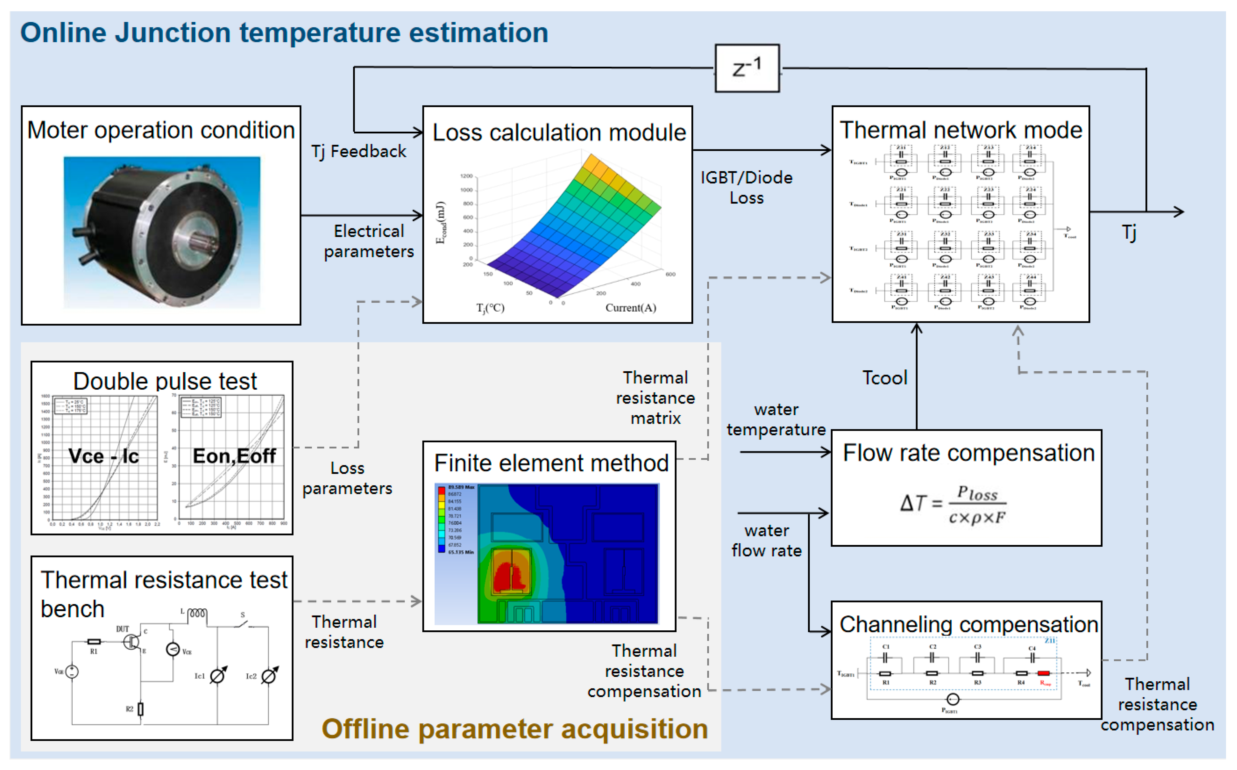
2. System Model Construction

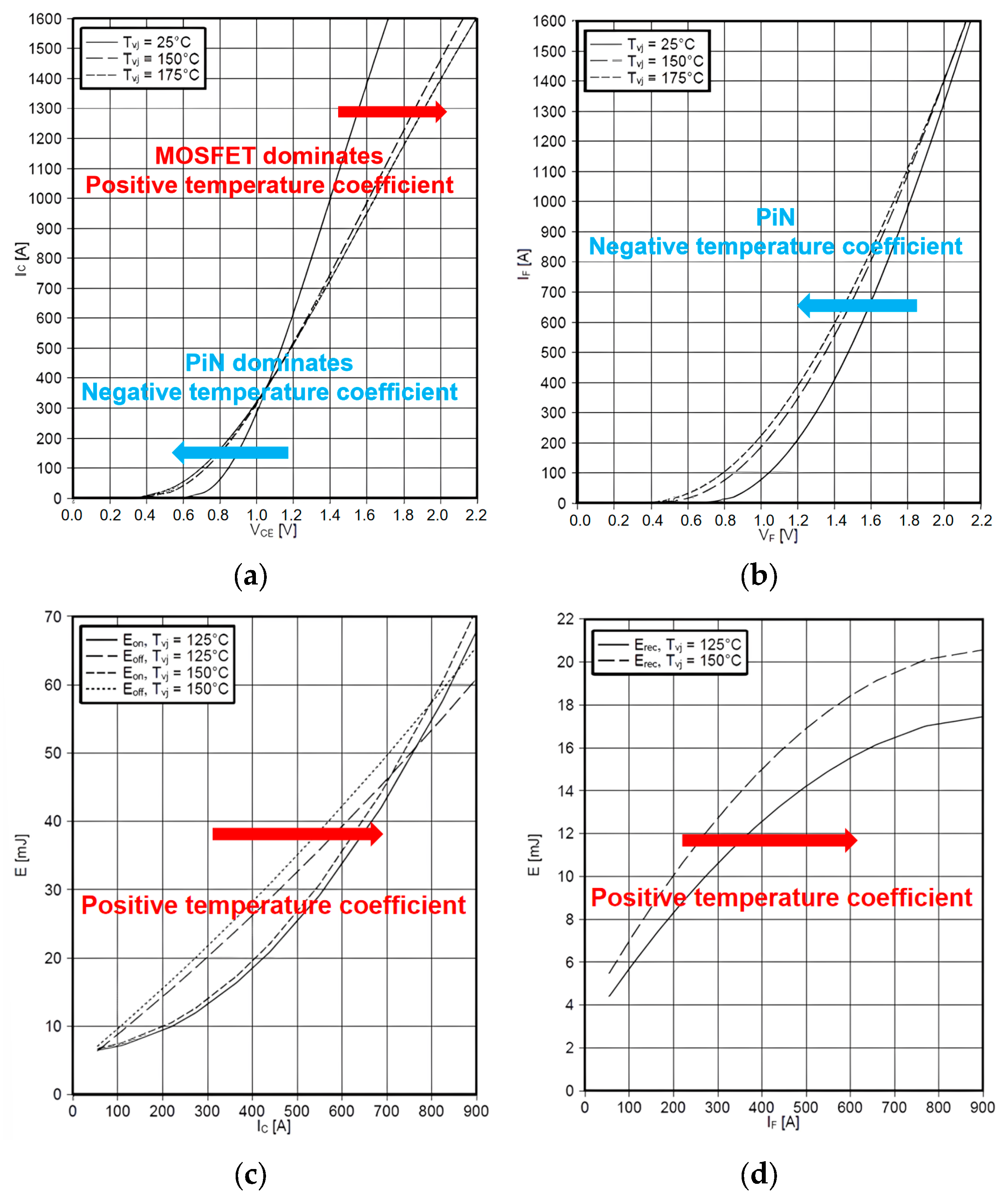
2.1. IGBT Power Loss Model

The heat loss in the IGBT module primarily arises from the IGBT power transistor and the freewheeling diode [29], including IGBT conduction loss, IGBT switching loss, diode conduction loss, and diode reverse recovery loss. The IGBT can be modeled as a PiN diode and a MOSFET operating in series in the linear region. Thus, the on-state voltage drop of the IGBT is the sum of the voltage drops across the PiN diode and the MOSFET. The voltage drop is calculated as follows:
V F , I G B T = V F , M O S F E T + V F , P i N
V F , M O S F E T = I C R C H
V F , P i N = 2 k T j q ln J c W N 4 q D a n i F W N 2 L a
where V F , I G B T , V F , M O S F E T , and V F , P i N represent the forward voltage drop of IGBT, MOSFET, and PiN diode respectively; I C represents the collector current, R C H represents the internal resistance, k represents the Boltzmann coefficient, T j represents the junction temperature of the IGBT, q represents the charge constant, and J c represents the collector current surface density. W N for drift zone width, D a for the bipolar diffusion coefficient, n i for intrinsic carrier density, L a for bipolar diffusion length.
Equations (1)–(3) can help to understand the relationship between voltage drop, current, and temperature. Figure 1a shows the typical conduction characteristic curve of the IGBT. At a high current, the MOSFET voltage drop dominates, resulting in a linear relationship between current and voltage. At low current, the PiN diode voltage drop dominates, leading to an exponential relationship between current and voltage. In terms of temperature, carrier drift motion predominates at a high current. As temperature increases, carrier mobility decreases, causing an increase in on-resistance and a positive temperature coefficient. At low current, PiN minority carrier expansion dominates, and diffusion is enhanced by rising temperature, which reduces the conduction voltage drop and results in a negative temperature coefficient. Figure 1b shows the typical conduction characteristic curve of the diode, which exhibits a negative temperature coefficient at both high and low currents. Figure 1c,d presents the switching loss curves for the IGBT and the diode, respectively. The relationship between switching loss and current is nonlinear, and the power loss increases with the device junction temperature.
Currently, the common conduction loss model uses linear fitting to approximate the relationship between current and voltage at high currents, which speeds up the calculation. However, since the temperature impact on conduction characteristics is nonlinear at different currents, linear fitting causes loss distortion at low currents. Therefore, a lookup table is used to obtain the required on-state loss and switching loss. The IGBT and diode losses in the loss model are calculated as follows:
P I G B T = d u t y · P c o n d + f s w · ( E o n + E o f f )
P D i o d e = d u t y · P c o n d + f s w · E r r
where duty represents the duty cycle, f s w represents the switching frequency, P c o n d represents the on-state loss of the IGBT or diode, and E o n and E o f f represent the on-state and off-state losses of the IGBT, respectively. E r r   represents the reverse recovery loss of the diode. The on-state and off-state losses of the device under different currents and temperatures can be obtained using static test equipment, and the on-state loss lookup table can be generated through double-pulse testing. During the online operation of the loss model, the transient loss value can be obtained by using the lookup table generated offline.

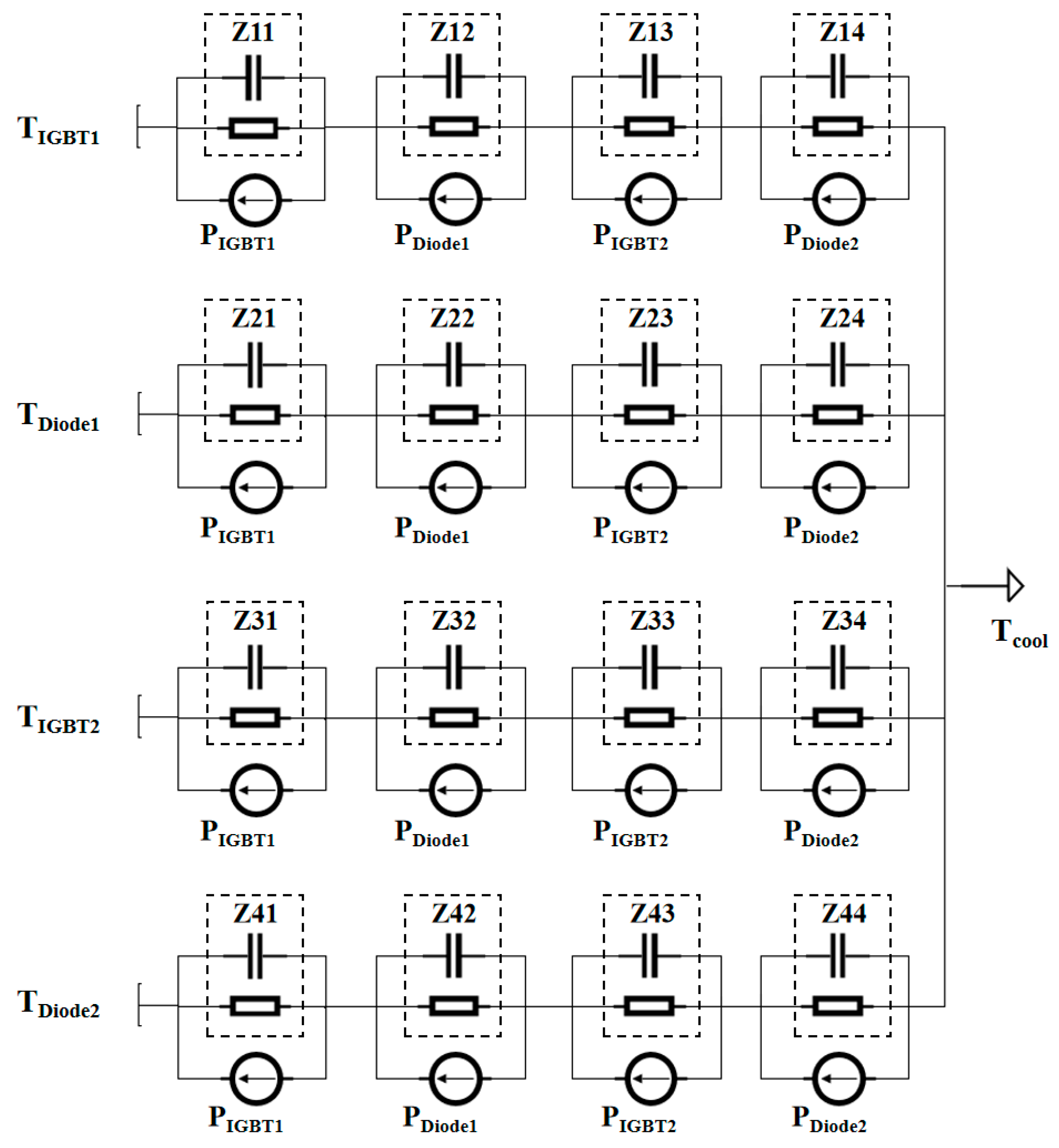
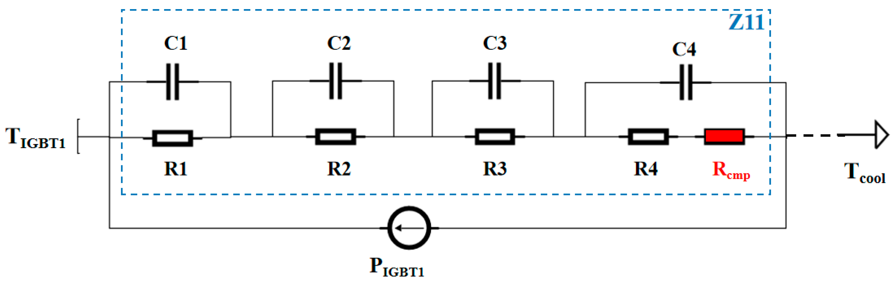
2.2. Thermal Network Model

Figure 2 shows the structure of a 750 V/600 A three-phase double-sided power module sandwiched between two heatsinks. Double-sided package modules enhance the electrical and mechanical properties of single-sided package modules [30]. This design reduces the thermal resistance and the stray inductance of the power module while also decreasing its volume and mass.
Single-sided package modules typically feature only one cooling boundary, resulting in a relatively straightforward heat dissipation path. In contrast, double-sided cooling (DSC) modules possess two distinct heat transfer paths, which are coupled simultaneously, leading to different boundary conditions. In the modeling process, the dual-channel heat transfer path of a DSC power module is often simplified into a parallel single-channel heat transfer path. The thermal network model is then established, with the thermal resistance of the two heat transfer channels obtained through two independent tests [31,32]. However, unlike single-sided cooling modules, the two heat transfer channels of DSC modules are not fully decoupled, causing the dual-channel thermal resistance to deviate from the parallel combination of the two single-channel thermal resistances, which introduces significant transient thermal resistance errors. Nonetheless, under ideal conditions, the heat flow ratio on both sides of the double-sided cooling module is unaffected by boundary conditions such as coolant flow and temperature. Therefore, a single Foster model can be used to model the double-sided cooling IGBT module.
The thermal impedance between the junction temperature and the reference point temperature can be expressed as follows:
Z t h = n = 1 N R n · ( 1 e t / τ )
T j ( t ) = Z t h · P l o s s ( t ) + T c o o l
where Z t h represents the total thermal impedance, R n represents the n-th order thermal resistance, τ = R n · C n represents the n-th order time constant, C n represents the n-th order heat capacity. Taking the fourth-order RC model as an example, with chip loss P l o s s and reference temperature T c o o l , the equation for estimating the junction temperature of a single chip can be written as follows:
d T d t = A T + B U
T j = C T + D U
T = T 1 T 2 T 3 T 4 ,   U = P l o s s T c o o l
A = 1 τ 1 0 0 0 0 1 τ 2 0 0 0 0 1 τ 3 0 0 0 0 1 τ 4 , B = 1 C 1 0 1 C 1 0 1 C 1 0 1 C 1 0
C = [ 1 1 1 1 ] , D = [ 0 1 ]
where A and B are the system matrix and input matrix; C and D are the output matrix and the feed matrix, respectively. ΔT represents the temperature rise of the chip, and Tn is the temperature rise corresponding to the n-th order RC. The formula can be discretized as follows:
T n ( k ) = ( T n ( k 1 ) · e t τ n ) + R n P ( k ) · ( 1 e t τ n )
T j ( k ) = T c o o l + 1 N T n ( k )
where k represents the current time step, k – 1 represents the previous time step, and Δt is the sampling step in time.
The junction temperature calculated using this formula only considers the heating of a single chip. However, in a traction inverter, the IGBT module is typically packaged in a 6-in-1 configuration, meaning multiple chips would generate losses during operation. The thermal coupling effect between different chips leads to a higher temperature rise for chips operating simultaneously compared to a single chip operating alone [33]. Figure 3 illustrates the chip distribution in a three-phase inverter. When calculating the junction temperature of a switch, it is necessary to account for the influence of adjacent IGBTs and diodes within the same phase, as well as the thermal coupling effects between different phases.
To address the thermal coupling of the chips packaged in the same power module, a thermal network model is established for four chips, considering the coupling between adjacent chips. Figure 4 illustrates the equivalent thermal resistance network, accounting for the thermal coupling between the four chips within the same phase-leg. PIGBT1, PDiode1, PIGBT2, and PDiode2 represent the loss values for the upper arm IGBT, upper arm diode, lower arm IGBT, and lower arm diode, respectively. TIGBT1, TDiode1, TIGBT2, and TDiode2 represent the junction temperatures of these four chips. Zij denotes the thermal impedance between chips I and j. When i and j are the same, it indicates self-thermal resistance; meanwhile, when i and j are different, it indicates coupling thermal resistance. Each Zij consists of a fourth-order RC model. The junction temperature of a chip can thus be calculated based on the losses of the four chips and the thermal resistance parameters between these chips. While a thermal network model can also be constructed to represent the thermal coupling between different phases by considering all 12 chips in a three-phase inverter, this method is more complex, requiring more parameters and increasing computational load. Since the mutual thermal influence between different phases is relatively small, and the inverter typically operates in a three-phase balanced state, it is sufficient to apply the thermal resistance parameters obtained for each phase collectively.
Thermal resistance parameters can be obtained using the finite element method and thermal resistance bench testing. The loss P1 is applied to the three upper bridge arm IGBTs, corresponding to the three phases. By analyzing the transient change in the junction temperature of the upper bridge arm IGBT, the self-heating impedance curve Z11(t) can be derived. From the temperature transient response curves of the other three chips, the coupled thermal impedance curves—Z21(t), Z31(t), and Z41(t)—representing the thermal impedance between the upper bridge IGBT and the other three chips can be obtained. Repeating this procedure allows the self-thermal resistance and coupling thermal resistance of all four chips to be calculated. The thermal impedance is expressed as follows:
Z i j ( t ) = T j _ i j ( t ) T r e f P j
where Z i j ( t ) represents the thermal impedance response of the j-th chip to the i-th chip, T j _ i j is the junction temperature of the upper bridge arm IGBT during the i-th test, P j is the loss value of the j-th chip, and T r e f represents the reference temperature. Each Zth can be fitted into a multi-order RC model based on the transient thermal resistance curve. Using this, the steady-state junction temperature of the upper bridge arm IGBT can be expressed as follows:
T i = T c o o l + ( Z 11 · P 1 + Z 12 · P 2 + Z 13 · P 3 + Z 14 · P 4 )
where T i represents the estimated junction temperature of chip i. By extending this formula to the four chips in the same phase, we can derive the thermal resistance network matrix that incorporates thermal coupling. The corresponding junction temperature formula is expressed as:
T 1 T 2 T 3 T 4 = T c o o l + Z 11 Z 12 Z 13 Z 14 Z 21 Z 22 Z 23 Z 24 Z 31 Z 32 Z 33 Z 34 Z 41 Z 42 Z 43 Z 44 · P 1 P 2 P 3 P 4
Combining Equations (9) and (13), the discretized junction temperature can be calculated as follows:
T j _ i ( k ) = T c o o l ( k ) +
T _ i ( k ) = j = 1 4 T _ i j ( k )
T _ i j ( k ) = n = 1 4 T _ i j n ( k )
T _ i j n ( k ) = T _ i j n ( k 1 ) · e t τ i j n + R i j n · P j ( k ) · ( 1 e t τ i j n )
where i represents the i-th chip, j represents the j-th chip thermally coupled with i-th chip, and n denotes the n-th order RC parameter. R i j n corresponds to the thermal resistance of order n, and τ i j n represents the associated time constant. T _ i indicates the temperature rise of chip i, T _ i j represents the temperature rise of chip i caused by chip j, and T _ i j n denotes the n-th order component of the temperature rise caused by chip j to chip i. Thus, the junction temperature calculation formula can be expressed in the following form:
T j _ i ( k ) = T c o o l ( k ) + j = 1 4 i = 1 4 ( T _ i j n ( k ) ) = T c o o l ( k ) + j = 1 4 i = 1 4 ( T _ i j n ( k 1 ) · e t τ i j n + R i j n · P j ( k ) · ( 1 e t τ i j n ) )

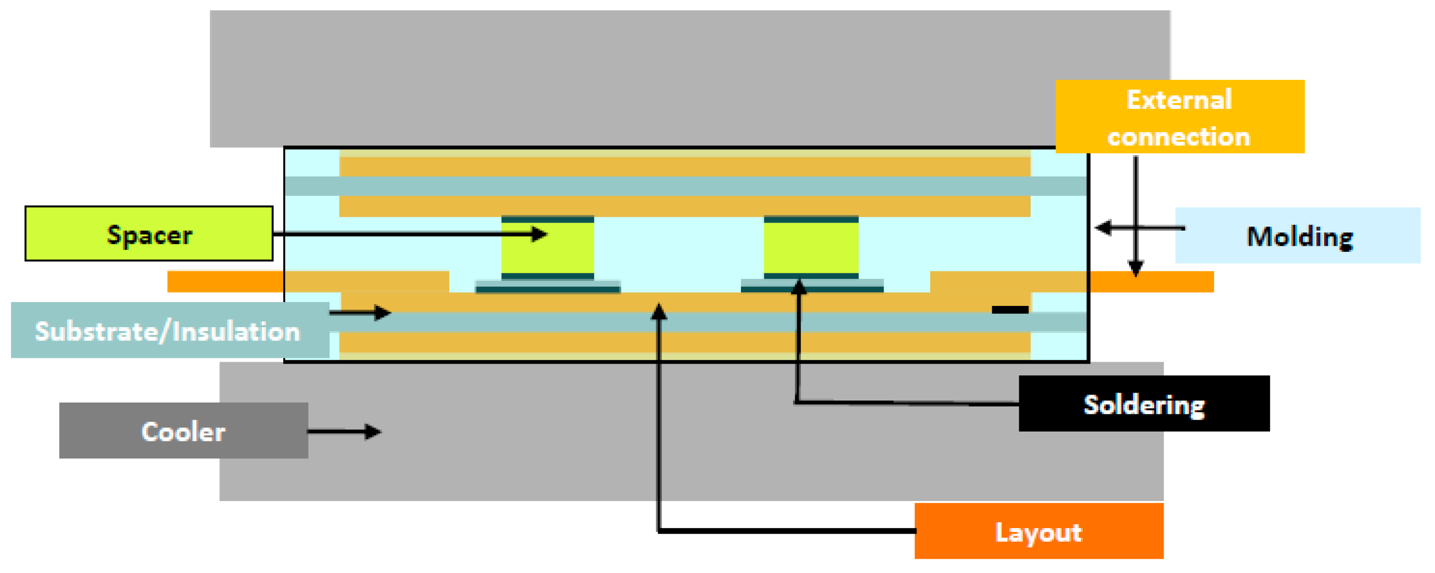
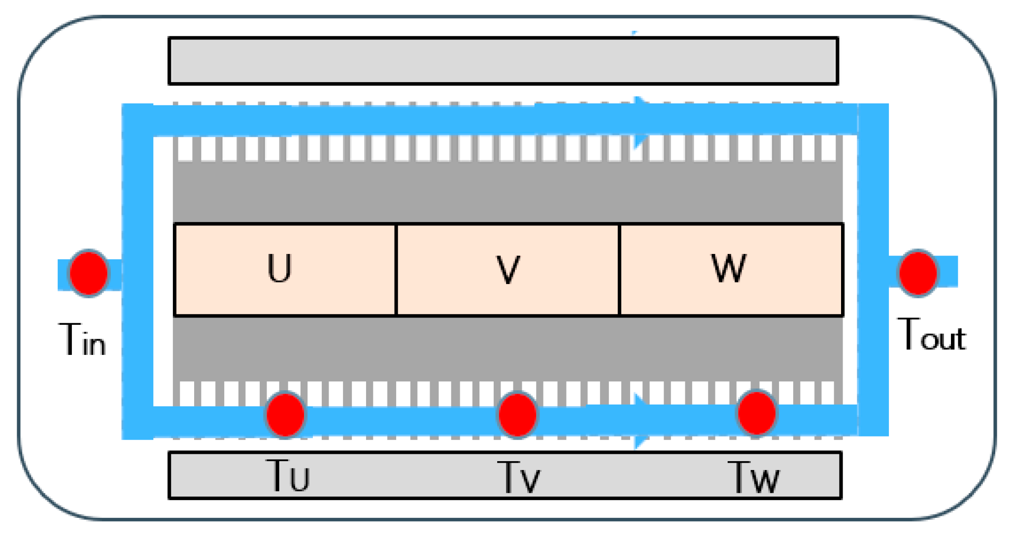
2.3. Model Optimization Considering Cooling Conditions

The boundary conditions of the power module vary during the actual operation of the motor controller. Since thermal resistance models differ under various cooling boundary conditions, it is essential to compensate for thermal resistance based on the prevailing cooling boundary conditions.
The schematic diagram of a three-phase inverter and its cooling water channel is shown in Figure 5. Theoretically, the extracted thermal resistance represents the resistance between the module and the temperature of the water channel directly below it. However, during actual operation, the water temperature increases along the channel, resulting in the outlet temperature T o u t being higher than the inlet temperature T i n . It can be approximated that the water temperature at the U-phase T u is roughly equal to the inlet temperature T i n , and the W-phase water temperature T w is approximately equal to the outlet temperature T o u t . Using T i n as a uniform reference temperature would underestimate the estimated temperature of the W-phase. To address this, compensation is acquired by calculating the temperature difference across the water channel based on the inlet temperature and flow rate F c o o l . The temperature difference is calculated as follows:
T c o o l = T o u t T i n ( k ) = P l o s s c · ρ · F c o o l
where T c o o l represents the temperature difference between the inlet and outlet, P l o s s denotes the total system loss, c is the specific heat capacity of the coolant, and ρ is the coolant density. During operation, the software calculates the real-time inlet-outlet temperature difference based on the actual system loss and flow rate. Using the computed temperature difference, the reference temperature for each phase is adjusted accordingly to ensure accurate thermal compensation.
Additionally, the thermal resistance parameters are influenced by the cooling boundary conditions. Typically, lower flow rates lead to higher thermal resistance. As a result, the thermal resistance matrix must be adjusted according to the cooling conditions.
In summary, the overall estimation model is depicted in Figure 6. The offline parameter acquisition process consists of two parts: the loss parameters are obtained through a double-pulse test, and the loss calculation model is introduced. Additionally, finite element simulations and thermal resistance bench tests are used to determine the thermal resistance matrix parameters, which are then incorporated into the thermal network model. During operation, the loss calculation model computes the transient loss value based on the input electrical parameters and the feedback junction temperature. The model then calculates the flow-compensated thermal resistance and the reference temperature for each phase, considering the cooling boundary conditions. Finally, the thermal network model estimates the junction temperature based on the input loss and reference temperature.

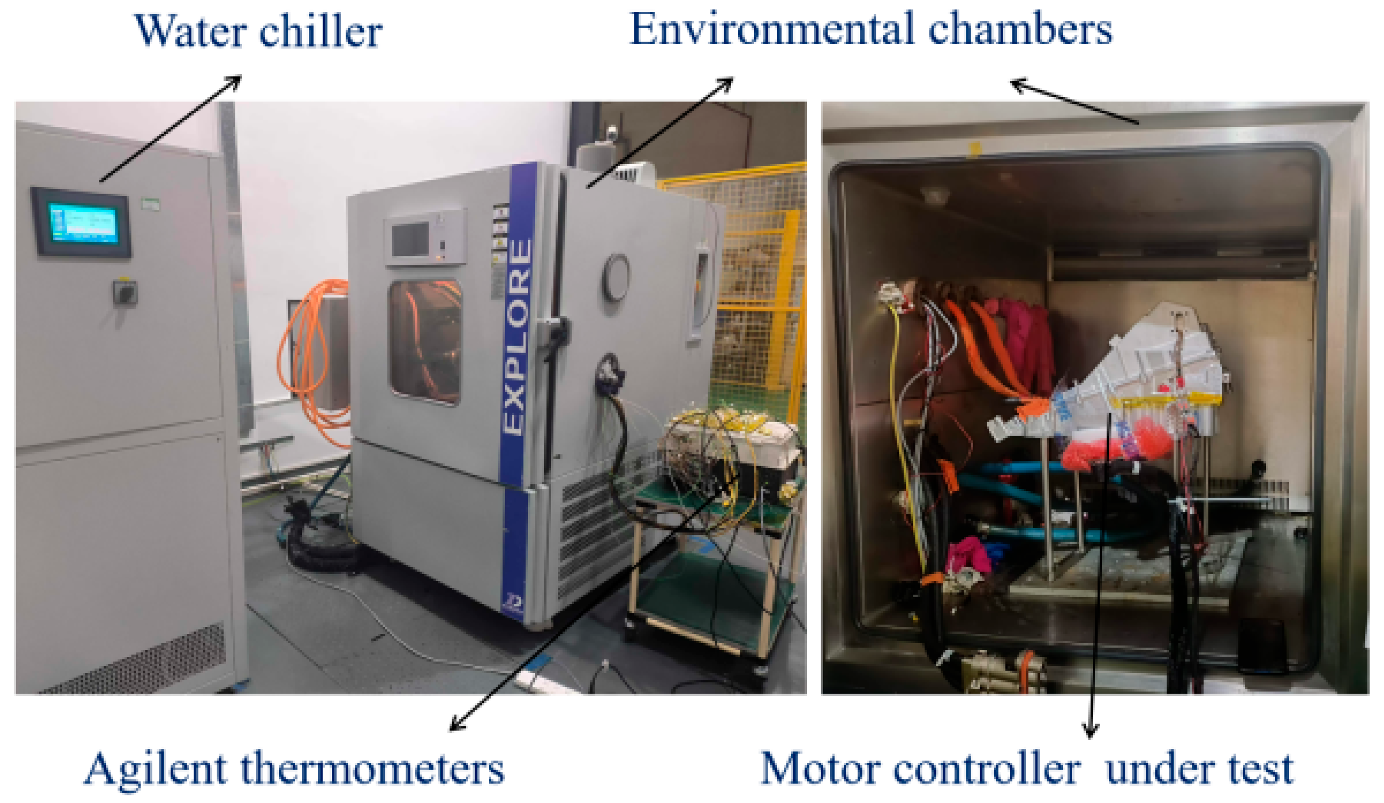
3. Parameter Acquisition and Experimental Verification

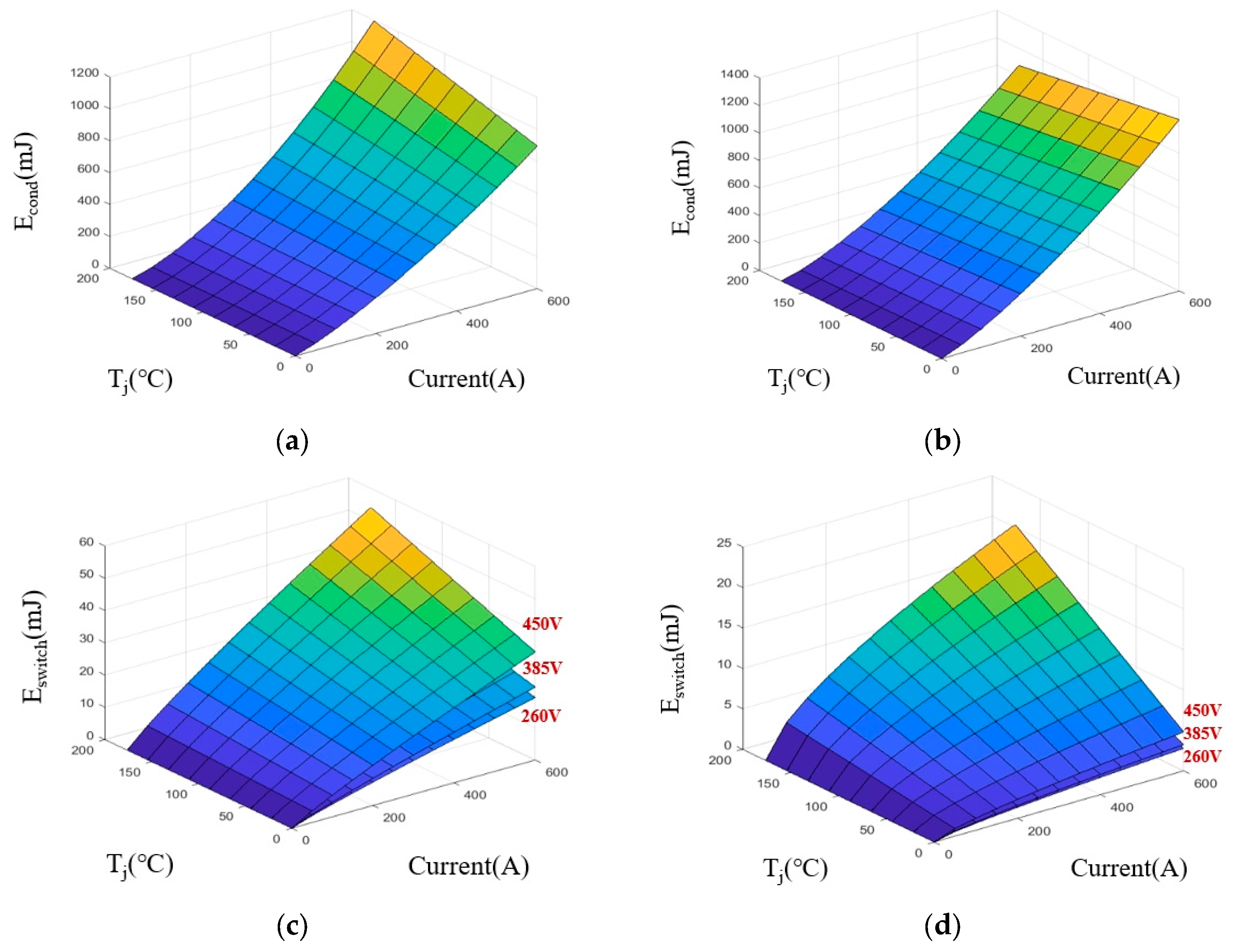
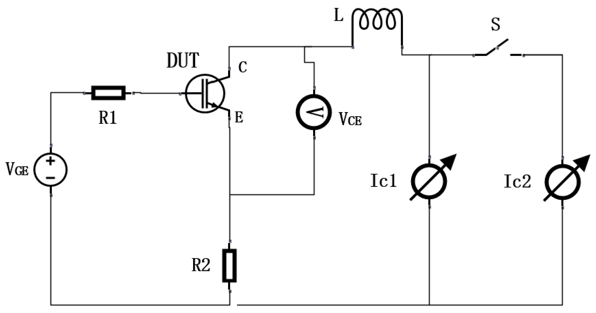
3.1. Loss Parameter Acquisition

Based on the previous analysis, the loss calculation module must first obtain the on-state and switching losses of the IGBTs and diodes offline. Figure 7 illustrates the 3D loss lookup chart derived from the double-pulse test. As shown in the figure, the relationship between the actual loss, junction temperature, and current aligns with the theoretical analysis. All losses are proportional to the current. The IGBT on-loss is inversely proportional to temperature at low currents and directly proportional to temperature at high currents. Diode conduction loss is consistently inversely proportional to temperature. The transient on-loss of the power module can be calculated based on the current and junction temperature during operation. Switching loss, however, is not only dependent on current and junction temperature but is also proportional to the bus voltage. Therefore, after calculating the switching loss, it must be adjusted according to the bus voltage.

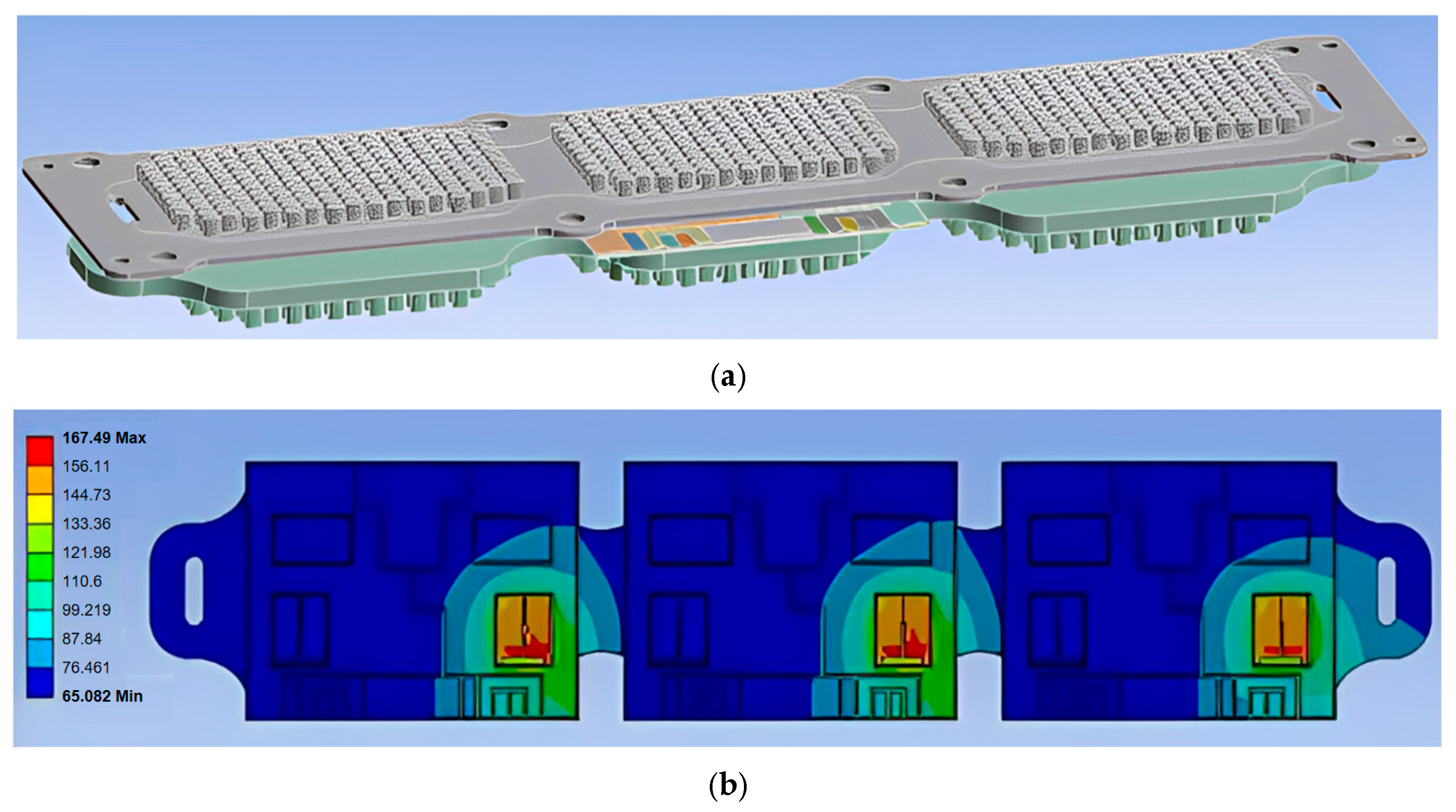
3.2. Obtain Thermal Resistance Parameters Using the Finite Element Method

For the thermal network model to be accurate, the thermal resistance parameter is one of the most important parameters to obtain. Thermal resistance parameters can be obtained based on the finite element simulation method mentioned above. In order to improve the accuracy of thermal resistance parameters, a thermal resistance parameter extraction method combining a finite element simulation and bench test is proposed in this paper. Bench testing is highly reliable and can be used to validate the accuracy of finite element models. Finite element simulations provide high flexibility and strong repeatability, allowing thermal resistance values under different conditions to be efficiently and repeatedly simulated by adjusting the model’s parameters and boundary conditions. Additionally, finite element simulations can assist in verifying the accuracy of junction temperature estimation. The time cost for a single finite element simulation is approximately 30 min. The thermal network model in MATLAB software (R2023a) takes about 5 s to run once, demonstrating favorable convergence properties.
The high-level flowchart is shown in Figure 8 and can be divided into three main steps. First, a thermal model is constructed based on the material parameters using commercial finite element simulation software. The self-thermal resistance and coupling thermal resistance parameters are then derived using the injection loss method. Next, the thermal resistance values of the module are measured using a thermal resistance test bench, and the finite element simulation thermal model is optimized based on the measured results until the simulation outputs align closely with the experimental data. Finally, the thermal model is adjusted to account for varying operational and cooling conditions by comparing the measured junction temperature with the temperature estimated by the thermal model.
Figure 9a presents the three-dimensional structure diagram of the finite element simulation corresponding to the three-phase inverter. Table 1 shows the material settings for finite element modeling. The boundary conditions are set as a 65 °C water temperature, an 8 L/min flow rate, and an average convective heat transfer coefficient of 4000 W/m2·K. The self-thermal resistance and coupling thermal resistance for each chip were determined by sequentially allocating power losses to the four chips.
Figure 9b shows the thermal cloud image when a 300 W loss is injected into the upper bridge arm IGBT. From the figure, it can be observed that the adjacent upper bridge arm diode exhibits a significant temperature rise, while the temperature rise in the IGBT and diode of the lower bridge arm is less pronounced. The corresponding thermal impedance value can be derived from the temperature response curve.
Figure 10 illustrates the temperature response curve and the corresponding self-thermal resistance curve for the IGBT in the bridge arm. The coupling thermal resistance between the IGBT and the adjacent diode is relatively large, while the coupling thermal resistance between the IGBT and the diode of the opposite bridge arm is smaller. The fourth-order RC parameters can be obtained through curve fitting, as shown in Table 1. From the data, it is evident that the first two thermal resistance values (Rth) of the coupling thermal resistance are quite small, suggesting a slow thermal coupling response of the chip. Therefore, the smaller two orders of the time constant in the coupling thermal resistance can be neglected, which also reduces the computational load of the model.
Table 2 represents a 4 × 4 order thermal impedance matrix. Each thermal impedance in the table is composed of a fourth-order thermal resistance and time constant, and each thermal impedance corresponds to Zij in Figure 4.

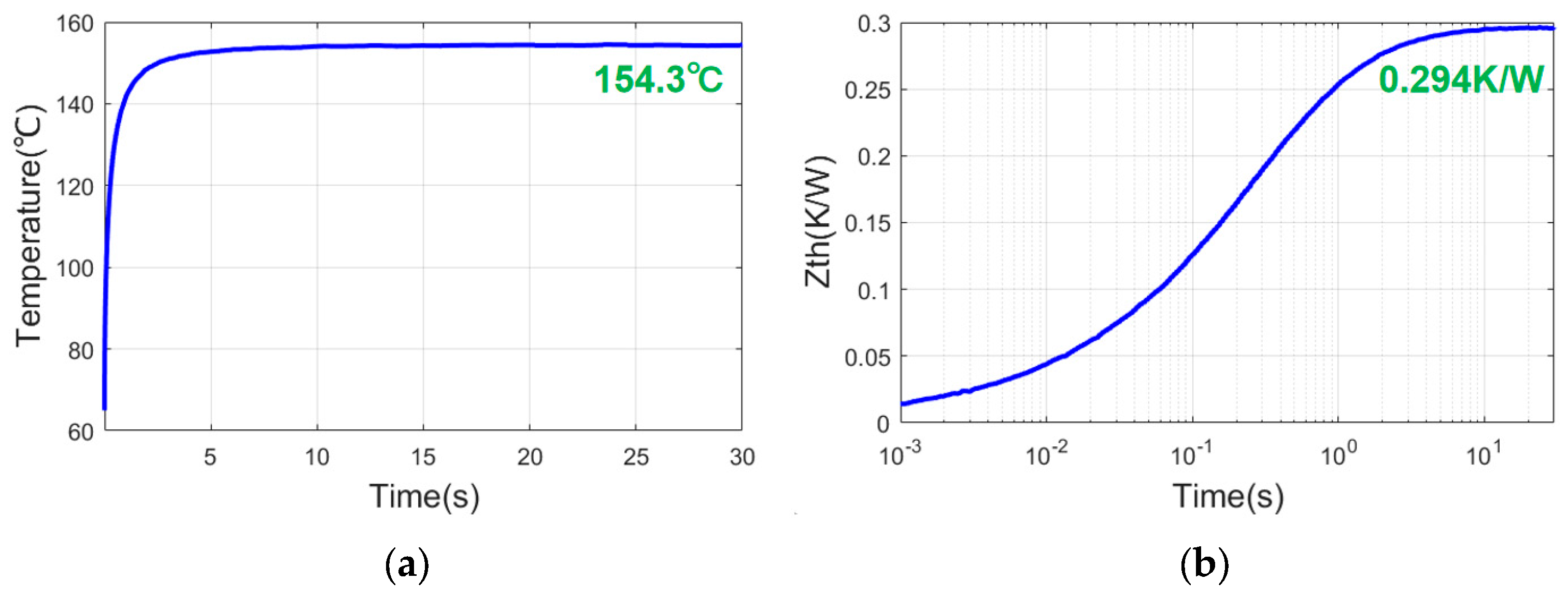
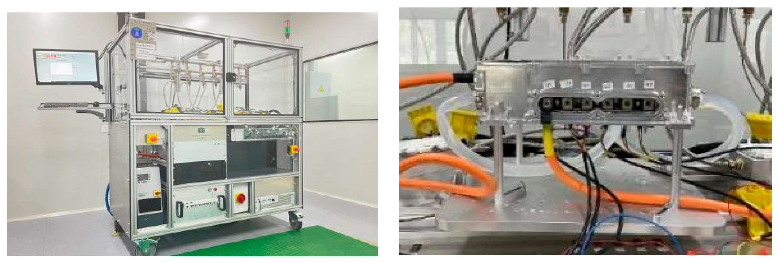
3.3. Thermal Resistance Test Platform Modified Thermal Model

The accuracy of the thermal resistance obtained through finite element simulation depends on the precision of the simulation model. Therefore, it is necessary to verify whether the junction temperature estimation model meets the required accuracy. This can be achieved by validating the simulation model and thermal resistance parameters using a thermal resistance test bench.
The thermal resistance test in this study primarily employs the TSEP method. As shown in Formula 1, when the IGBT is switched on at a high current, the first term in the voltage drop formula dominates. At a low current (100 mA), the first term becomes negligible, and the second term prevails, causing the IGBT collector current to increase exponentially with the on-voltage drop. In this scenario, the relationship between the saturation voltage drop UCE and junction temperature Tj is approximately negative. This principle forms the basis of the junction temperature estimation method using the saturation voltage UCE as the thermally sensitive electrical parameter. However, since this method requires disconnecting the load current, it is not suitable for online junction temperature measurement and is typically used for offline testing.
Figure 11 shows the thermal resistance test bench and the IGBT module to be tested. The junction temperature of the chip is obtained using the TSEP method, and the thermal resistance value of the module can be calculated according to the junction temperature. Different coolant temperatures and flow rates can be set through the water channel. Figure 12 illustrates the circuit diagram for measuring the junction temperature thermal resistance using the low-current saturation voltage drop method. The device under test (DUT) is the switching device being evaluated. Initially, the power module is passively heated by increasing the coolant temperature, while a constant test current Ic1 is supplied to the module. The low-current saturation voltage drop is then measured at various temperatures, from which the calibration curve and the K coefficient are derived.
Next, the device is heated using a high current Ic2, and the junction temperature is adjusted by varying the current. The case temperature T c is dynamically observed and recorded until it stabilizes, at which point the pressure drop V c e is recorded. The high current I c 2 is then disconnected by the switch at time ton, and the pressure drop and shell temperature variations during the cooling process are recorded in real time. Finally, the junction temperature T j is calculated using the K coefficient. Figure 13 illustrates the current and temperature curves for the test process. The thermal impedance is then calculated as follows:
Z t h ( t ) = T j ( t ) T c ( t ) P l o s s = T j ( t ) T c ( t ) V c e I c 2
The accuracy of the finite element thermal model can be validated by comparing the thermal resistance parameters obtained from the thermal resistance bench with those from the simulation. The steady-state thermal resistance deviation between the simulation and measurement is within 1.5%, indicating the high accuracy of the thermal resistance parameters.

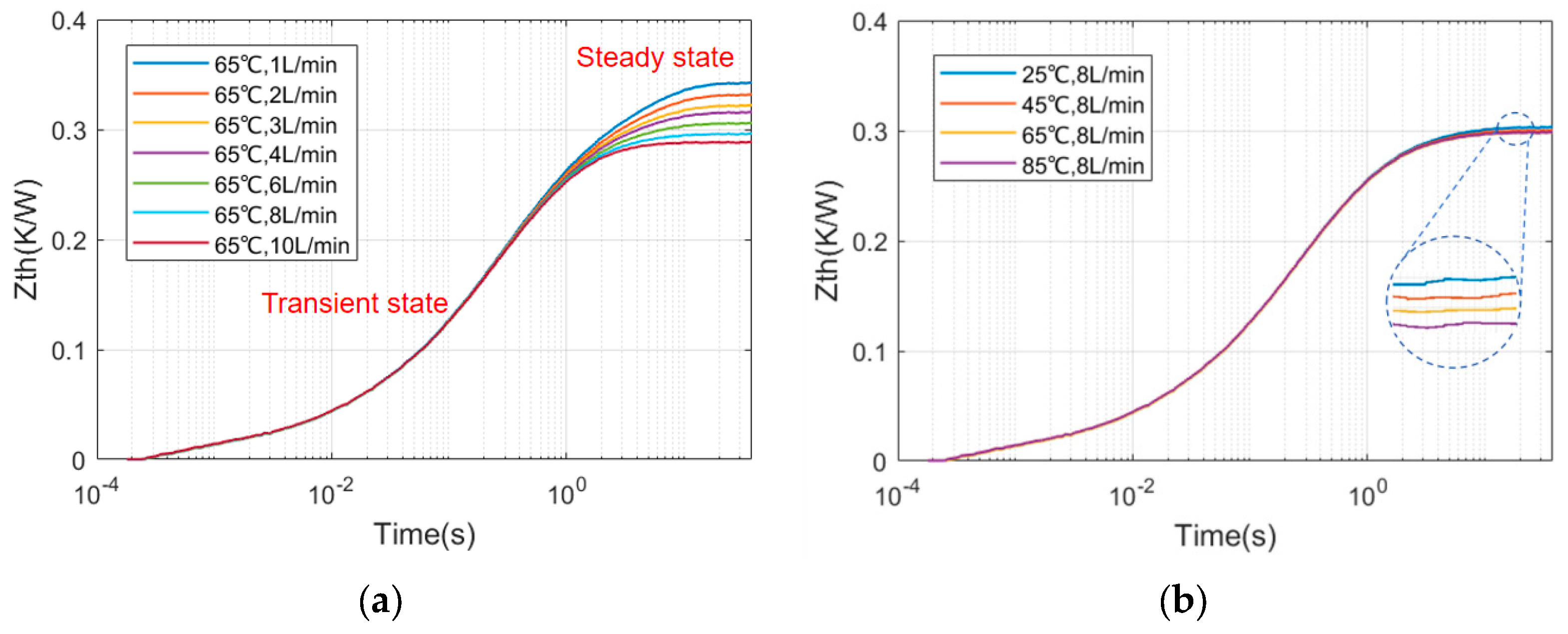
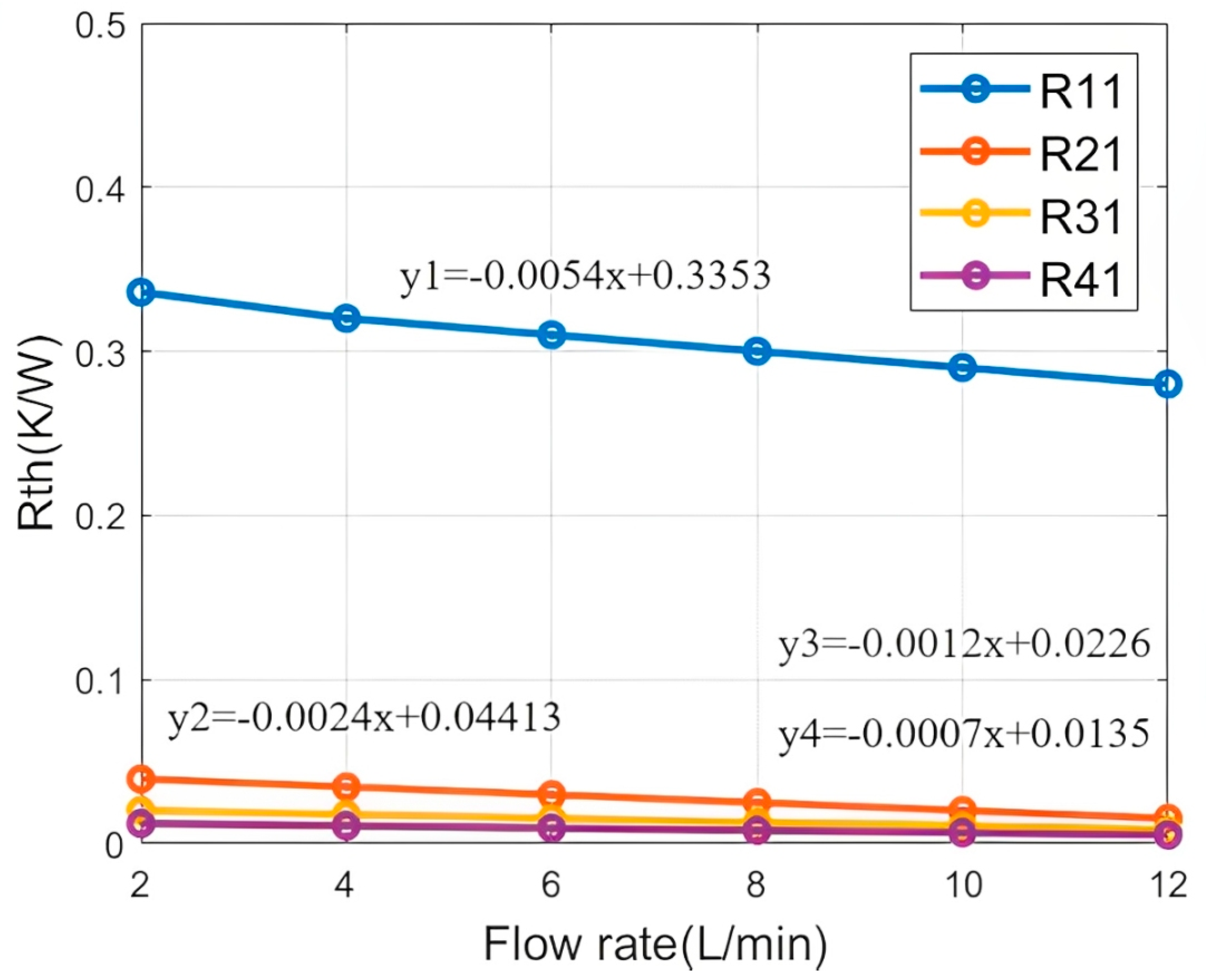
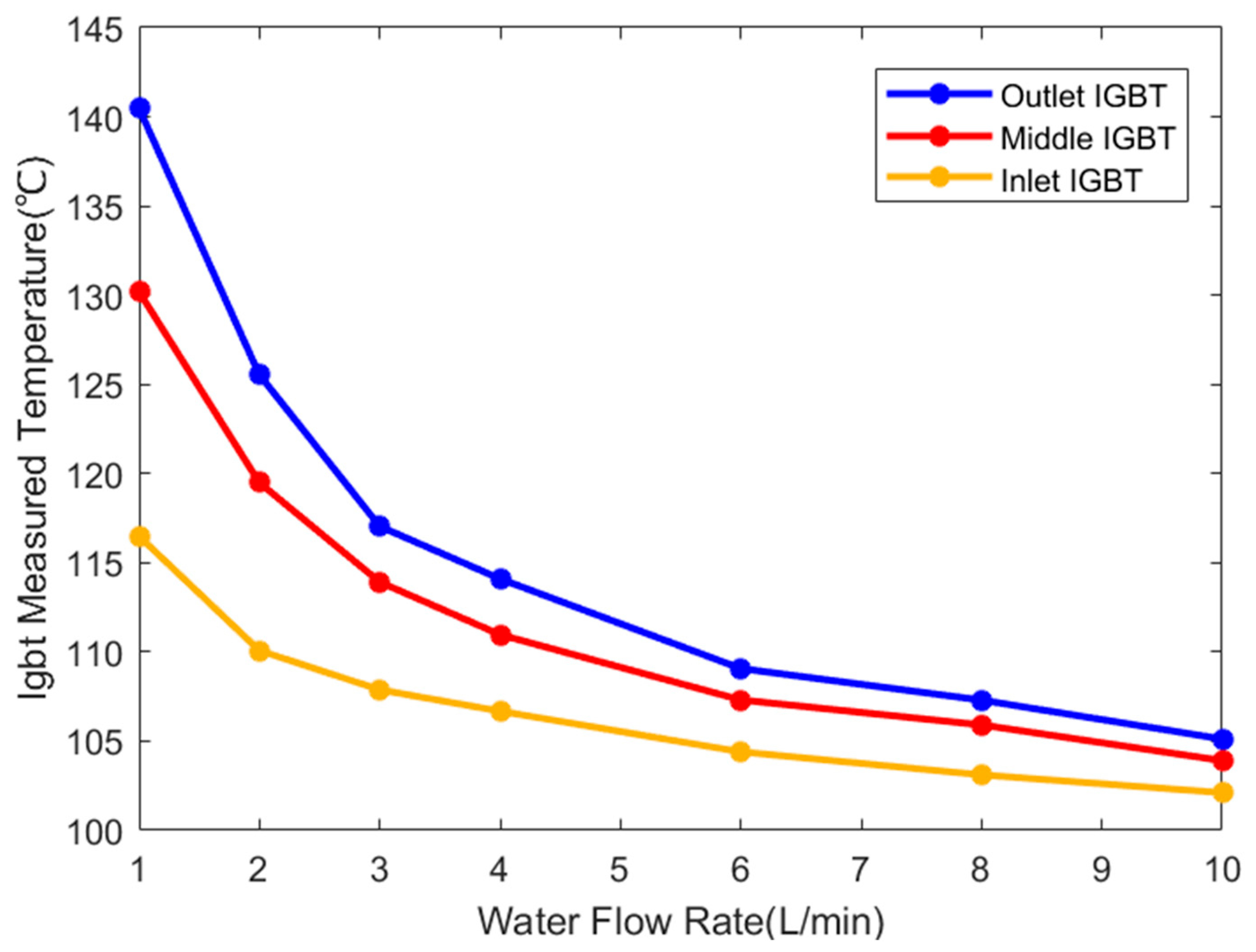
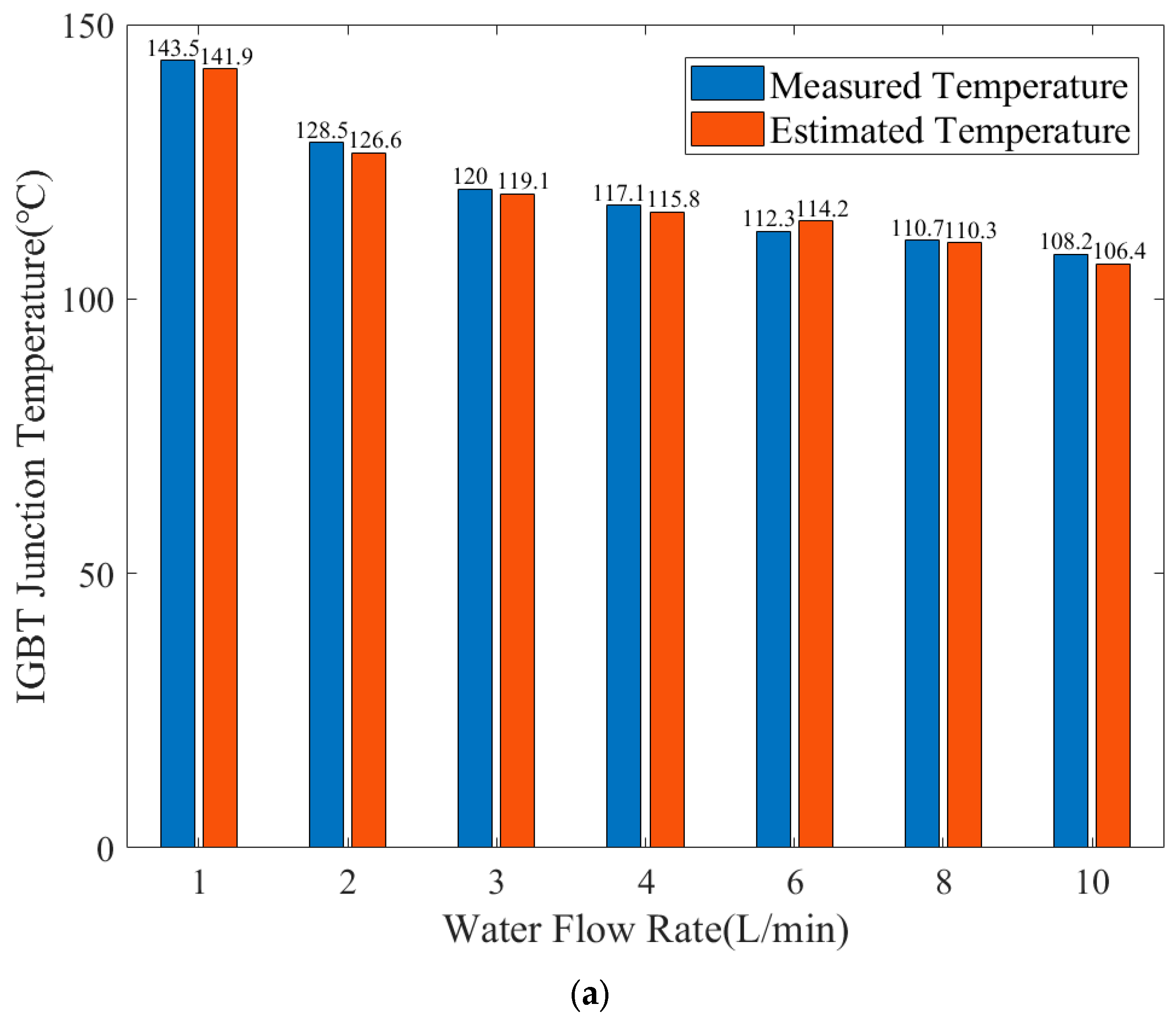
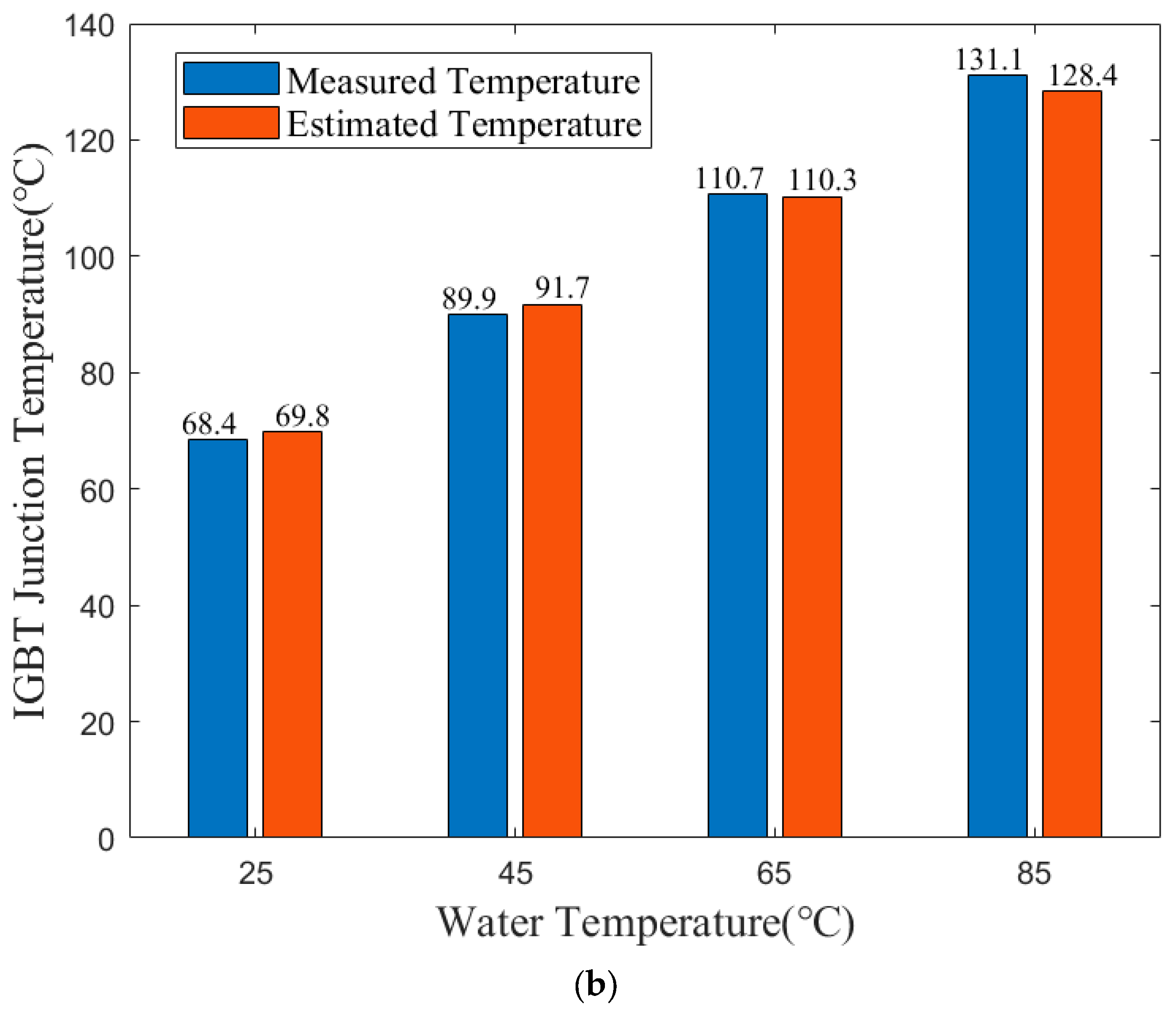
3.4. Cooling Condition-Based Thermal Resistance Parameters Compensation

The influence of cooling boundary conditions on the thermal network cannot be overlooked. Thermal resistance test data under different cooling conditions can be obtained using a combination of simulation and experiment. Figure 14 presents the thermal resistance test curves at different water temperatures and flow rates. As shown in Figure 14a, the self-thermal resistance varies with flow rates, with the impact most evident in the steady state (where the time constant is large). As flow velocity increases, the system reaches a steady state more quickly, and the steady thermal resistance decreases. The coupling thermal resistance between the IGBT and adjacent diodes at different flow rates follows a similar trend as the self-thermal resistance. Figure 14b shows that the thermal resistance decreases only slightly with increasing temperature, and the effect on the final estimated junction temperature is almost negligible. Therefore, the influence of water temperature can be neglected in the subsequent analysis.
Figure 15 illustrates the variation in thermal resistance at different water flow rates. R11 represents the relationship between the steady-state self-thermal resistance and flow rate of the IGBT on the bridge. R21, R31, and R41 represent the relationships between the steady-state coupling thermal resistances and flow for the upper bridge IGBT to the upper bridge diode, as well as the lower bridge IGBT to the lower bridge diode, respectively. The figure shows that the change in steady-state thermal resistance across different water flows can be approximately linearized within a small range.
Based on the previous conclusion that the influence of the flow rate on thermal resistance is primarily observed in the steady state, the model can be compensated for the term with the largest time constant in the fourth-order RC thermal resistance model. This term, which is most affected by the coolant flow rate, is also the one located closest to the coolant. Figure 16 illustrates the self-thermal resistance network after compensating for cooling conditions. Here, Rn and C n represent the n-th steady-state thermal resistance and heat capacity values, with C4 corresponding to the term with the highest time constant. A thermal resistance compensation term R c m p , calculated based on the coolant flow rate, is added to the fourth-order thermal resistance R4. The value of R c m p can be obtained using steady-state thermal resistance values at different flow rates. Consequently, the temperature rise of the chip can be expressed as the sum of the chip’s heating temperature rise and the flow compensation temperature rise. After corrections to Equations (17) and (18), the junction temperature calculation formula can be expressed as follows:
T j i k = T c o o l k + j = 1 4 T i j k + T i j c m p k = T c o o l ( k ) + j = 1 4 ( i = 1 4 ( T _ i j n ( k ) + T _ i j c m p ( k ) )
T i j n k = T i j n k 1 · e t τ i j n + R i j n · P j k · 1 e t τ i j n
T i j c m p k = T i j c m p k 1 · e t τ i j 4 + R i j c m p · P j k · 1 e t τ i j 4
where T i j n represents the n-th order temperature rise caused by the j-th chip to the i-th chip, and T _ i j c m p represents the temperature rise compensation value of the j-th chip to the i-th chip. Rijcmp is the compensation value for the fourth-order thermal resistance from the j-th chip to the i-th chip, with its corresponding time constant being the largest time constant of the fourth-order RC. This estimated junction temperature, based on the formula, can be adjusted according to the coolant flow rate, making it applicable to a wider range of operating conditions.

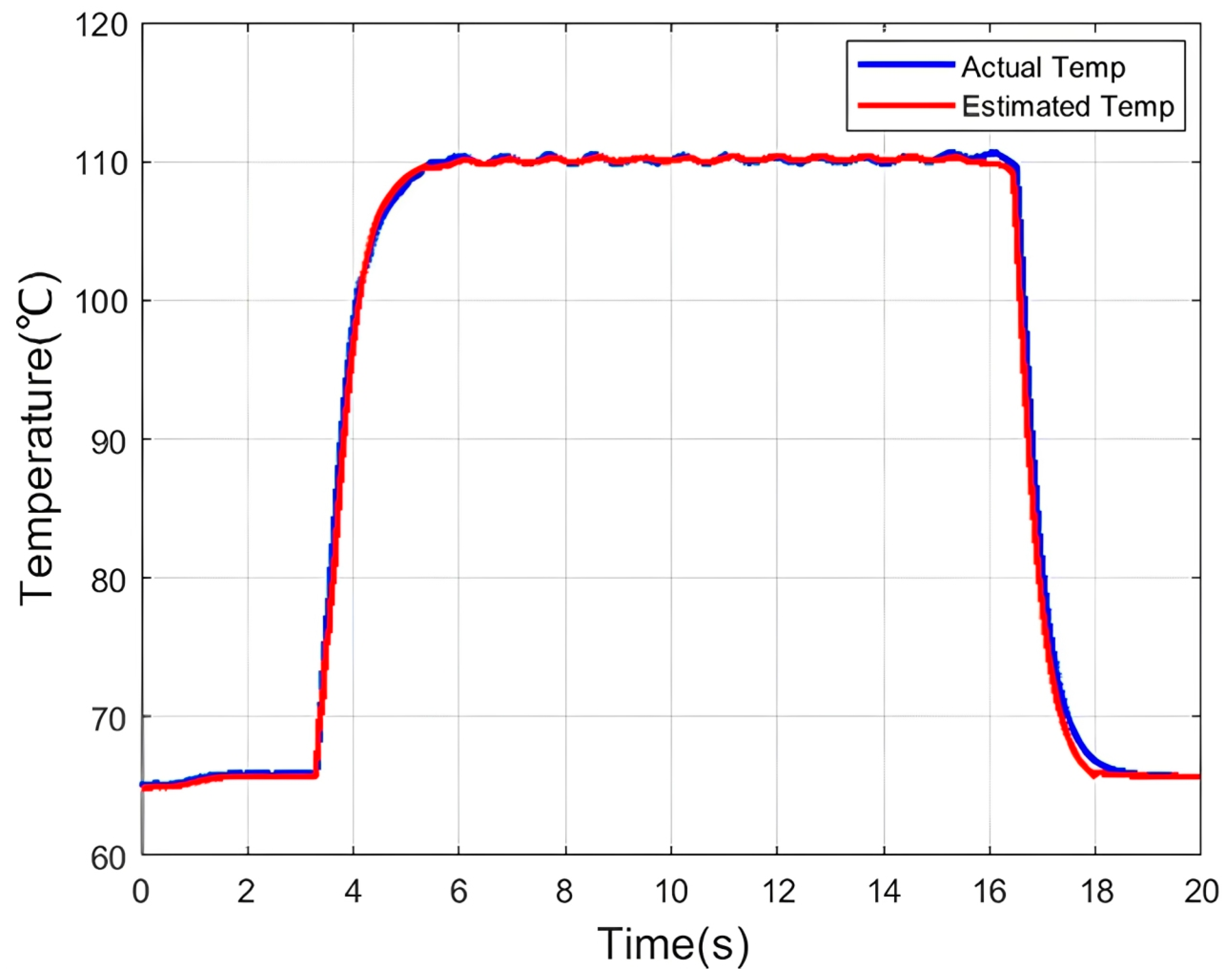
3.5. Bench-Top Verification

To validate the accuracy of the junction temperature estimation method presented in this paper, a motor controller-inductance load test platform was built, as shown in Figure 17. The ambient temperature is controlled via an EXPLORE environmental chamber, and the coolant temperature and flow rate are regulated using an LNEYA water chiller (Wuxi Guanya Refrigeration Technology Co., Ltd., Wuxi, Jiangsu, China). The temperature of the coolant can be measured using Agilent thermometers (Agilent Technologies, Inc; Santa Clara, CA, USA). An IGBT module equipped with an on-chip temperature sensor is employed to monitor the temperature during operation. The maximum operating junction temperature of the IGBT is 175 °C. Key parameters influencing IGBT heating include current, voltage, switching frequency, power factor angle, and modulation scheme. By selecting an appropriate external inductance load for the motor, the heating conditions of the IGBT can be effectively evaluated during the motor’s forward operation.
The upper computer is used to set the ambient temperature to 85 °C, the coolant temperature to 65 °C, and the coolant flow rate to 8 L/min. The inverter operates in Constant Current Variable Frequency (CCVF) mode, with a switching frequency of 10 kHz and a fundamental frequency of 300 Hz. The junction temperature estimation is verified under different operating conditions by varying the voltage and current.
Figure 18 presents the schematic diagram of the measured maximum junction temperature of the sensor under the rated voltage of 385 V and current of 250 A. Since the sensor measures the average temperature of the chip, the average temperature estimated by the software is also used for comparison. As shown in the figure, both the dynamic and static errors of the software estimate are within 5 °C. Overheating is a significant cause of IGBT failure, making accurate temperature estimation during peak conditions crucial. Table 3 provides the test data for different voltage and current combinations. The total inverter loss varies synchronously with the rise in IGBT temperature. It is evident that the temperature estimation error for various voltage and current levels is around 3 °C. Even under peak conditions of 450 V and 350 A, the estimation error does not exceed 3 °C.
To investigate the effect of cooling boundary conditions on junction temperature estimation, experiments were conducted by setting different water temperatures and flow rates in the chiller. The ambient temperature was set to 85 °C, the water temperature to 65 °C, the bus voltage to 385 V, the current to 250 A, the switching frequency to 10 kHz, and the fundamental frequency to 300 Hz. The flow rates were gradually set to 1 L/min, 2 L/min, 3 L/min, 4 L/min, 6 L/min, 8 L/min, and 10 L/min. The flow rate was maintained for a sufficient period until the temperature stabilized, allowing the study of the influence of flow rate changes on junction temperature.
Figure 19 shows the measured steady-state average temperature of the three-phase IGBT at different flow rates. As observed, the IGBT temperature at the outlet is higher than at the inlet, and the temperature difference between the outlet and inlet IGBT increases as the flow rate decreases. At a flow rate of 1 L/min, the temperature difference exceeds 20 °C, highlighting the necessity of flow rate compensation. Additionally, the inlet IGBT temperature increases with the decrease in flow rate, which is attributed not only to the chip’s inherent heat but also to the increased thermal resistance caused by the reduced flow rate. The figure also shows that the temperature difference across the three-phase IGBT follows a roughly isometric distribution, meaning the reference temperatures for the intermediate and outlet phases can be compensated based on the inlet temperature and loss. Since the focus is on the highest temperature within the module, this study primarily compares the outlet phase IGBT temperature. However, in certain operating conditions, the highest temperature IGBT may not be in the outlet phase, necessitating the monitoring of each phase IGBT. Figure 20a presents the statistics of the estimated IGBT temperature and the sensor-measured temperature at different flow rates. The figure shows that as the flow rate increases, the IGBT temperature decreases, with the estimated error remaining within 5 °C.
Figure 20b shows the statistical comparison of the estimated IGBT temperature and the sensor-measured temperature under different water temperatures. The bus voltage was set to 385 V, current to 250 A, switching frequency to 10 kHz, and fundamental frequency to 300 Hz. The water temperature was successively set to 25 °C, 45 °C, 65 °C, and 85 °C. The figure demonstrates that the estimation error for different water temperatures remains within 5 °C.

4. Conclusions

This paper presents a method for accurately estimating the junction temperature of double-sided cooling insulated-gate bipolar transistor (IGBT) modules, incorporating thermal boundary conditions and chip-level thermal coupling effects. By analyzing chip distribution and the impact of cooling boundaries on the thermal model, the proposed method offers reliable junction temperature estimation under various operating conditions. To improve the accuracy of thermal resistance parameters, a novel parameter extraction method is introduced, combining ANSYS (2024R1) finite element simulations and thermal resistance tests. The effects of different cooling boundaries on thermal resistance parameters are systematically examined through simulations and experiments, revealing that coolant temperature has minimal influence, while the effect of flow rate on thermal resistance is more than 20%. Lower flow rates result in higher thermal resistance and intensify the heat channeling effect within the module. The proposed thermal model dynamically adjusts its parameters in response to varying cooling conditions. Experimental validation conducted under diverse operating conditions using an inductance test bench confirms that the junction temperature estimation error of the proposed method is within 5 °C for double-sided cooling IGBT modules.

Author Contributions

G.L. and M.L. managed the project and conceptualized the idea; M.C. designed the energy management strategy, completed the modeling, simulation, and bench experiments; M.C. wrote the manuscript. S.C., S.W. and H.B. contributed to validations and analyses of the results and reviewed the writing. All authors have read and agreed to the published version of the manuscript.

Funding

This research received no external funding.

Data Availability Statement

The data are not publicly available due to privacy.

Conflicts of Interest

Authors Mengfan Chen, Shouzhong Chang, Sirui Wu and Huichuang Bao were employed by the Leadrive Technology (Shanghai) Co., Ltd. The remaining author declares that the research was conducted in the absence of any commercial or financial relationships that could be construed as a potential conflict of interest.

Nomenclature

SymbolDescriptionUnit
P I G B T Loss of IGBTJ
P D i o d e Loss of DiodeJ
Z i j Thermal impedance response of the j-th chip to the i-th chipK/W
T j _ i Junction temperature of chip i°C
T _ i Temperature rise of chip i°C
T _ i j Temperature rise of chip i caused by chip j°C
T _ i j n The n-th order component of the temperature rise caused by chip j to chip i°C
T _ i j c m p Temperature rise compensation value of the j-th chip to the i-th chip°C
R i j n The n-th order thermal resistance value in Z i j K/W
τ i j n The n-th order time constant value in Z i j s
R i j c m p The resistance compensation value for the 4th order thermal resistance in Z i j K/W

References

  1. Ning, P.; Wen, X. A Double-Sided Cooling Package Design with Pinfin. In Proceedings of the PCIM Asia 2017; International Exhibition and Conference for Power Electronics, Intelligent Motion, Renewable Energy and Energy Management, Shanghai, China, 27–29 June 2017; pp. 1–7. [Google Scholar]
  2. Zhou, F.; Zhou, Y.; Fan, T.; Dede, E.M. Double-Side Manifold Micro-Channel Cold Plate for High Power Density Composite DC-DC Converter. In Proceedings of the 2023 22nd IEEE Intersociety Conference on Thermal and Thermomechanical Phenomena in Electronic Systems (ITherm), Orlando, FL, USA, 30 May–2 June 2023; pp. 1–8. [Google Scholar] [CrossRef]
  3. Liu, M.; Coppola, A.; Alvi, M.; Anwar, M. Comprehensive Review and State of Development of Double-Sided Cooled Package Technology for Automotive Power Modules. IEEE Open J. Power Electron. 2022, 3, 271–289. [Google Scholar] [CrossRef]
  4. Pai, A.P.; Ebli, M.; Simmet, T.; Lis, A.; Beninger-Bina, M. Characteristics of a SiC MOSFET-based Double Side Cooled High Performance Power Module for Automotive Traction Inverter Applications. In Proceedings of the 2022 IEEE Transportation Electrification Conference & Expo (ITEC), Anaheim, CA, USA, 15–17 June 2022; pp. 831–836. [Google Scholar] [CrossRef]
  5. Zhou, J.; Yu, Y.; Zheng, L.; Du, X.; Wang, J.; Ren, H.; Peng, Y. Online Noninvasive Technique for Condition Monitoring of Cooling System in Urban Rail Vehicles. IEEE Trans. Ind. Electron. 2023, 70, 12762–12772. [Google Scholar] [CrossRef]
  6. Fernández, M.; Perpiñà, X.; Vellvehi, M.; Aviñó-Salvadó, O.; Llorente, S.; Jordà, X. Power Losses and Current Distribution Studies by Infrared Thermal Imaging in Soft- and Hard-Switched IGBTs Under Resonant Load. IEEE Trans. Power Electron. 2020, 35, 5221–5237. [Google Scholar] [CrossRef]
  7. Zhang, W.; Qi, L.; Tan, K.; Ji, B.; Zhang, X.; Chai, W.; Cui, X. IGBT Junction Temperature Estimation Using a Dynamic TSEP Independent of Wire Bonding Faults. IEEE Trans. Power Electron. 2023, 38, 5323–5334. [Google Scholar] [CrossRef]
  8. Guo, W.; Ma, M.; Wang, H.; Chen, Q.; Wang, H.; Song, Q.; Chen, W. Decoupling Compact Thermal Model in Multichip IGBT Modules: A Methodology Based on Concepts of Positive and Negative Mutual Thermal Coupling. IEEE J. Emerg. Sel. Top. Power Electron. 2024, 12, 5476–5492. [Google Scholar] [CrossRef]
  9. Wang, Z.; Qiao, W.; Qu, L. A Real-Time Adaptive IGBT Thermal Model Based on an Effective Heat Propagation Path Concept. IEEE J. Emerg. Sel. Top. Power Electron. 2021, 9, 3936–3946. [Google Scholar] [CrossRef]
  10. Wang, H.; Qiao, W.; Qu, L. A Thermal Network Model for Multichip Power Modules Enabling to Characterize the Thermal Coupling Effects. IEEE Trans. Power Electron. 2024, 39, 6225–6245. [Google Scholar] [CrossRef]
  11. Bruckner, T.; Bernet, S. Estimation and measurement of junction temperatures in a three-level voltage source converter. In Proceedings of the 40th IAS Annual Meeting. Conference Record of the 2005 Industry Applications Conference, Hong Kong, China, 2–6 October 2005; pp. 106–114. [Google Scholar] [CrossRef]
  12. Chai, X.; Ning, P.; Cao, H.; Zheng, D.; Li, H.; Huang, Y.; Kang, Y. Online Junction Temperature Measurement of Double-sided Cooling IGBT Power Module through On-state Voltage with High Current. Chin. J. Electr. Eng. 2022, 8, 104–112. [Google Scholar] [CrossRef]
  13. Xu, Z.; Xu, F.; Wang, F. Junction Temperature Measurement of IGBTs Using Short-Circuit Current as a Temperature-Sensitive Electrical Parameter for Converter Prototype Evaluation. IEEE Trans. Ind. Electron. 2015, 62, 3419–3429. [Google Scholar] [CrossRef]
  14. Avenas, Y.; Dupont, L.; Khatir, Z. Temperature Measurement of Power Semiconductor Devices by Thermo-Sensitive Electrical Parameters—A Review. IEEE Trans. Power Electron. 2012, 27, 3081–3092. [Google Scholar] [CrossRef]
  15. Tang, T.; Song, W.; Yang, K.; Chen, J. A Junction Temperature Online Monitoring Method for IGBTs Based on Turn-off Delay Time. IEEE Trans. Ind. Appl. 2023, 59, 6399–6411. [Google Scholar] [CrossRef]
  16. Arya, A.; Chanekar, A.; Deshmukh, P.; Verma, A.; Anand, S. Accurate Online Junction Temperature Estimation of IGBT Using Inflection Point Based Updated I–V Characteristics. IEEE Trans. Power Electron. 2021, 36, 9826–9836. [Google Scholar] [CrossRef]
  17. Yun, C.-S.; Malberti, P.; Ciappa, M.; Fichtner, W. Thermal component model for electrothermal analysis of IGBT module systems. IEEE Trans. Adv. Packag. 2001, 24, 401–406. [Google Scholar] [CrossRef]
  18. van der Broeck, C.H.; Lorenz, R.D.; De Doncker, R.W. Monitoring 3-D Temperature Distributions and Device Losses in Power Electronic Modules. IEEE Trans. Power Electron. 2019, 34, 7983–7995. [Google Scholar] [CrossRef]
  19. Schweitzer, D.; Chen, L. Heat spreading revisited—Effective heat spreading angle. In Proceedings of the 2015 31st Thermal Measurement, Modeling & Management Symposium (SEMI-THERM), San Jose, CA, USA, 15–19 March 2015; pp. 88–94. [Google Scholar] [CrossRef]
  20. Feng, X.-Y.; Bai, F.; Ding, H.; Tao, W.-Q. An improved POD-Galerkin method for rapid prediction of three-dimensional temperature field for an IGBT module. Int. Commun. Heat Mass Transf. 2024, 152, 107241. [Google Scholar] [CrossRef]
  21. Baliga, B.J. Analytical Modeling of IGBTs: Challenges and Solutions. IEEE Trans. Electron Devices 2013, 60, 535–543. [Google Scholar] [CrossRef]
  22. Zhang, J.; Du, X.; Yu, Y.; Zheng, S.; Sun, P.; Tai, H.-M. Thermal Parameter Monitoring of IGBT Module Using Junction Temperature Cooling Curves. IEEE Trans. Ind. Electron. 2019, 66, 8148–8160. [Google Scholar] [CrossRef]
  23. Bahman, A.S.; Ma, K.; Blaabjerg, F. General 3D lumped thermal model with various boundary conditions for high power IGBT modules. In Proceedings of the 2016 IEEE Applied Power Electronics Conference and Exposition (APEC), Long Beach, CA, USA, 20–24 March 2016; pp. 261–268. [Google Scholar] [CrossRef]
  24. Górecki, K.; Górecki, P. SPICE-Aided Nonlinear Electrothermal Modeling of an IGBT Module. Electronics 2023, 12, 4588. [Google Scholar] [CrossRef]
  25. Yang, X.; Heng, K.; Dai, X.; Wu, X.; Liu, G. A Temperature-Dependent Cauer Model Simulation of IGBT Module With Analytical Thermal Impedance Characterization. IEEE J. Emerg. Sel. Top. Power Electron. 2022, 10, 3055–3065. [Google Scholar] [CrossRef]
  26. Lu, Y.; Xiang, E.; Jin, Y.; Luo, H.; Yang, H.; Li, W.; Zhao, R. A 3-D Temperature-Dependent Thermal Model of IGBT Modules for Electric Vehicle Application Considering Various Boundary Conditions. IEEE J. Emerg. Sel. Top. Power Electron. 2024, 12, 5463–5475. [Google Scholar] [CrossRef]
  27. Akbari, M.; Bahman, A.S.; Bina, M.T.; Eskandari, B.; Iannuzzo, F.; Blaabjerg, F. A Multi-Layer RC Thermal Model for Power Modules Adaptable to Different Operating Conditions and Aging. In Proceedings of the 2018 20th European Conference on Power Electronics and Applications (EPE’18 ECCE Europe), Riga, Latvia, 17–21 September 2018; pp. P.1–P.10. [Google Scholar]
  28. Heng, K.; Yang, X.; Wu, X.; Ye, J. A 3-D Thermal Network Model for Monitoring of IGBT Modules. IEEE Trans. Electron Devices 2023, 70, 653–661. [Google Scholar] [CrossRef]
  29. Liu, L.; Bao, M.; Zhang, L.; Fan, X.; Tang, D. Power Loss Calculation Method for IGBT in Converter Valve Based on Inverse Heat Transfer Problem. In Proceedings of the 2021 IEEE 2nd China International Youth Conference on Electrical Engineering (CIYCEE), Chengdu, China, 15–17 December 2021; pp. 1–5. [Google Scholar] [CrossRef]
  30. Mandray, S.; Guichon, J.-M.; Schanen, J.-L.; Guyennet, M.M.; Dienot, J.-M. Electromagnetic Considerations for Designing Double-Sided Power Modules. IEEE Trans. Ind. Appl. 2009, 45, 871–879. [Google Scholar] [CrossRef]
  31. Guo, C.; Cui, S.; Tsai, W.; Liu, Y.; Ding, J.; Li, J.; Chen, Z.; Li, Y.; Pan, S.; Feng, S. Measuring Double-Sided Thermal Resistance of Press-Pack IGBT Modules Based on Ratio of Double-Sided Heat Dissipation. IEEE Trans. Electron Devices 2023, 70, 1776–1781. [Google Scholar] [CrossRef]
  32. Chen, J.; Deng, E.; Zhang, Y.; Huang, Y. Junction-to-Case Thermal Resistance Measurement and Analysis of Press-Pack IGBTs Under Double-Side Cooling Condition. IEEE Trans. Power Electron. 2022, 37, 8543–8553. [Google Scholar] [CrossRef]
  33. Zhang, X.; Tong, X.; Lv, C.; Du, S.; Chen, K.; Wu, K.; Li, J. A 3-D Thermal Network Model for IGBT Modules Considering Temperature Dependence of Heat Dissipation and Thermal Coupling. In Proceedings of the 2024 IEEE 10th International Power Electronics and Motion Control Conference (IPEMC2024-ECCE Asia), Chengdu, China, 17–20 May 2024; pp. 4906–4910. [Google Scholar] [CrossRef]
Figure 1. (a) I–V static characteristic of IGBT; (b) I–V static characteristic of diode; (c) switching loss versus current curve of IGBT; (d) switching loss versus current curve of diode.
Energies 18 01785 g001
Figure 2. Double-sided water-cooled module structure.
Energies 18 01785 g002
Figure 3. Chip distribution of three-phase inverter.
Energies 18 01785 g003
Figure 4. Equivalent thermal network model considering thermal coupling.
Energies 18 01785 g004
Figure 5. Three-phase inverter water channel diagram.
Energies 18 01785 g005
Figure 6. Junction temperature estimation model.
Energies 18 01785 g006
Figure 7. (a) Three-dimensional curve of IGBT conduction loss; (b) three-dimensional curve of diode conduction loss; (c) three-dimensional curve of IGBT switching loss; (d) three-dimensional curve of diode switching loss.
Energies 18 01785 g007
Figure 8. Thermal resistance extraction flow chart.
Energies 18 01785 g008
Figure 9. (a) Three-dimensional structure diagram of finite element simulation; (b) thermal cloud diagram.
Energies 18 01785 g009
Figure 10. (a) Temperature response of top IGBT under step loss; (b) transient thermal impedance curve of top IGBT.
Energies 18 01785 g010
Figure 11. Thermal resistance test benches and module assembled with cooler.
Energies 18 01785 g011
Figure 12. TSEP thermal resistance test circuit diagram.
Energies 18 01785 g012
Figure 13. (a) Thermal resistance test current curve; (b) thermal resistance test temperature curve.
Energies 18 01785 g013
Figure 14. (a) Self-thermal resistance curves at different flows; (b) self-thermal resistance curves at different temperatures.
Energies 18 01785 g014
Figure 15. Thermal resistance trend diagram at different flow rates.
Energies 18 01785 g015
Figure 16. Thermal network model after cooling condition compensation.
Energies 18 01785 g016
Figure 17. Motor controller and inductive load test platform.
Energies 18 01785 g017
Figure 18. Junction temperature estimation error curve.
Energies 18 01785 g018
Figure 19. Temperature variation of different IGBTs with flow velocity.
Energies 18 01785 g019
Figure 20. (a) Experimental results at different flow rates; (b) experimental results at different water temperatures.
Energies 18 01785 g020aEnergies 18 01785 g020b
Table 1. Finite element model material settings.
LayerMaterialThickness
(mm)
Density
(g/cm3)
Thermal Conductivity
(W/m*K)
Specific Heat
(J/g*K)
Outer_baseplateAl3003\2.741600.893
Outer_TIMTIM0.152.702.20.800
Outer_Cu1Cu0.408.963800.381
Outer_CeramicZTA0.32 4.00200.720
Outer_Cu2Cu0.308.963800.381
Spacer_solder1SnSb50.107.40550.230
SpacerWCu2.3215.52000.170
Spacer_solder2SnSb50.107.40550.230
ChipSi0.082.3398.90.741
Chip_solderSnSb50.17.40550.230
Inner_Cu2Cu0.308.963800.381
Inner_CeramicZTA0.32 4.00200.720
Inner_Cu1Cu0.408.963800.381
Inner_TIMTIM0.152.702.20.800
Inner_baseplateAl6063\2.722000.896
Al6061\2.721550.896
Table 2. Thermal impedance matrix parameters.
Top IGBTTop DiodeBot IGBTBot Diode
Top IGBTRthτRthτRthτRthτ
0.038450.001454.3 × 10−70.014.32 × 10−70.0093.5 × 10−60.009
0.074240.037887 × 10−130.13.9 × 10−100.13.8 × 10−90.099
0.06780.23060.0064120.22280.00173410.0014291
0.112610.042121.5320.0048063.4270.0037743.278
Top DiodeRthτRthτRthτRthτ
9.6 × 10−70.0090.018750.001655.42 × 10−70.0094.51 × 10−60.009
9 × 10−120.0990.059870.041224.2 × 10−100.0993.84 × 10−90.1
0.051460.2140.057890.21060.00283410.0026971
0.006681.6890.101410.0037863.3260.0048843.297
Bot IGBTRthτRthτRthτRthτ
5.03 × 10−70.017.1 × 10−70.010.029780.002017.8 × 10−120.009
6.4 × 10−110.14.6 × 10−130.10.079450.040134.5 × 10−90.099
0.0019810.00281210.061240.22560.0021890.1947
0.007653.1470.0031793.3320.126910.041341.624
Bot DiodeRthτRthτRthτRthτ
6.5 × 10−80.016.14 × 10−60.017.7 × 10−120.0090.028120.00171
5.6 × 10−110.17.4 × 10−110.16.34 × 10−90.0990.064780.03325
0.0015110.0047810.0013640.20230.042150.2314
0.003193.0490.001153.1980.0041451.6780.10981
Table 3. Estimation error at different voltages and currents.
Bus
Voltage
(V)
Load
Current
(A)
Fundamental Frequency
(Hz)
Inverter
Loss
(J)
Measured
Temperature
(°C)
Estimated
Temperature
(°C)
Error
(°C)
38510030056783.9784.310.34
3852503001612111.65110.321.33
3853503002889147.62149.311.69
385350502896148.32148.890.57
2603503001964120.12121.351.23
4503503003325160.34158.411.93
Disclaimer/Publisher’s Note: The statements, opinions and data contained in all publications are solely those of the individual author(s) and contributor(s) and not of MDPI and/or the editor(s). MDPI and/or the editor(s) disclaim responsibility for any injury to people or property resulting from any ideas, methods, instructions or products referred to in the content.

