Article

Preparation of Highly Efficient and Stable All-Inorganic Perovskite Solar Cells in Atmosphere Environment

by
Yufan Jiang
,
Dongdong Deng
and
Jingjing Dong
*
School of Science, China University of Geosciences, Beijing 100083, China
*
Author to whom correspondence should be addressed.
Energies 2025, 18(9), 2162; https://doi.org/10.3390/en18092162
Submission received: 21 March 2025 / Revised: 14 April 2025 / Accepted: 21 April 2025 / Published: 23 April 2025

Abstract

:
All-inorganic CsPbX3 perovskites have significant potential for applications in the photovoltaic field. However, during their preparation, the slow evaporation rate of the precursor solution limits the extent of solution supersaturation, leading to porous perovskite films that substantially impair device performance. Anti-solvent engineering, which introduces a secondary solvent to modulate the crystallization process, is a well established technique in perovskite photovoltaic research. This study systematically examines the effects of four different anti-solvents on perovskite films and corresponding devices. It also investigates the optimal dipping-time of (trifluoromethyl)benzene as an anti-solvent, as well as the impact of varying amounts of anti-solvent additive perfluorinated acid. The optimized devices achieved a maximum power conversion efficiency of 12.68%.

1. Introduction

In recent years, perovskite materials have garnered significant attention due to their unique characteristics, including long carrier diffusion lengths and low exciton binding energies. Among them, all-inorganic CsPbX3 perovskites stand out for their superior stability, enhanced efficiency, simpler fabrication processes, advanced optical modulation capabilities, and better environmental compatibility compared with organic–inorganic hybrid perovskites [1,2,3,4]. To date, the power conversion efficiencies (PCEs) of pure CsPbI3 perovskite solar cells have reached 21.8% [5]. These advantages render them highly promising for applications in optoelectronic devices [6].
Despite their rapid rise in the solar cell industry for high efficiency and cost-effectiveness [7], perovskite solar cells still face major challenges, particularly in achieving long-term stability and reliability—critical factors for commercial viability [8,9,10,11]. In parallel with efforts to optimize material design and device architecture, increasing attention has been paid to fabrication process engineering, especially thin film processing techniques [12,13,14,15].
Among these, anti-solvent treatment has emerged as a key step for improving the quality and stability of perovskite thin films [16,17]. This method involves introducing a secondary solvent (anti-solvent) to control the crystallization behavior of perovskite precursors during film formation [18,19]. The anti-solvent lowers solute solubility, leading to supersaturation and nucleation, and plays a decisive role in defining crystal size, shape, and film uniformity [20,21,22,23,24,25,26,27,28]. In spin-coating processes, anti-solvent engineering facilitates dense and uniform film formation. Furthermore, by tuning the type of anti-solvent and processing parameters such as volume, dripping time, and temperature, researchers can effectively tailor the film morphology and improve optoelectronic properties including light absorption, charge carrier mobility, and device performance [29,30,31,32,33,34].
In this work, we investigate the effect of different anti-solvent treatments on the performance of all-inorganic CsPbI1.8Br1.2 perovskite solar cells. Four anti-solvents—chlorobenzene (CB), isopropanol (IPA), ethyl acetate (EA), and (trifluoromethyl)benzene (TFT)—were selected for a comparative study. Among them, TFT yielded the highest optical and structural film quality, resulting in the best photovoltaic conversion efficiency. Further optimization was conducted by incorporating trifluoroacetic acid (PFA) as an additive into the TFT anti-solvent system, ultimately achieving a maximum PCE of 12.68% for the optimized device.

2. Experimental Section

2.1. Materials and Reagents

Lead(II) iodide (PbI2), lead(II) bromide (PbBr2), and Cesium iodide (CsI) were brought from Xi’an Polymer Light Technology Corp. The titanium dioxide (TiO2) slurry was supplied by Kaitou New Energy Co., Ltd., Huai An, China. The low-temperature carbon paste (doctor blading/screen printing) was purchased from Beijing Huamin New Materials Co., Ltd., Beijing, China. The rest of the materials, including ethanol (ET, 99.5%), isopropanol (IPA, 99.5%), chlorobenzene (CB, 99.5%), ethyl acetate (EA, 99.5%), (trifluoromethyl)benzene (TFT), and trifluoroacetic acid (PFA), were purchased from Aladdin (Shanghai, China). All materials were used without further purification.

2.2. Fabrication of Carbon-Based CsPbI1.8Br1.2 PSCs

In our previous study, we detailed the cleaning process for fluorine-doped tin oxide (FTO) substrates, as well as the fabrication procedures for a compact titanium dioxide (c-TiO2) layer and a mesoporous titanium dioxide (m-TiO2) layer. These steps are critical for ensuring the high-quality preparation of subsequent layers in the device structure [35].
The CsPbI1.8Br1.2 film was fabricated using a one-step spin-coating method. CsI, PbBr2, and PbI2 were weighed according to their stoichiometric ratios and dissolved in dimethyl sulfoxide (DMSO). For example, 311.77 mg of CsI, 264.25 mg of PbBr2, and 221.28 mg of PbI2 were added to 1 mL of DMSO. The precursor solution was obtained by stirring the mixture at 70 °C for several hours. The solution was then spin-coated onto the substrate, followed by 60 °C for 5 min and 200 °C for 20 min annealing to form the perovskite thin film. Finally, carbon paste was used as the electrode material and printed through a 100-mesh screen template. After printing the carbon paste, the device underwent low-temperature annealing at 120 °C for 15 min, resulting in the fabrication of CsPbI1.8Br1.2 perovskite solar cells.

2.3. Characterization of Perovskite Solar Cells

Under one-sun illumination provided by a solar simulator (scs10-X150-DZ), device performance was tested by applying an external bias to obtain the open-circuit voltage (VOC) and short-circuit current density (JSC). The experimental data were processed using Origin software to calculate the power conversion efficiency (PCE) and fill factor (FF) of the perovskite solar cells. The electrical performance data were further correlated with material characterization, including X-ray diffraction (XRD, Rigaku D/MAX-2500, Tokyo, Japan), scanning electron microscopy (SEM, Hitachi S-4800, Tokyo, Japan), steady-state photoluminescence (PL), transient photoluminescence (TRPL), and UV-visible absorption spectroscopy (Cary 5000 UV-vis spectrophotometer, Agilent, Santa Clara, CA, USA). These techniques were used to analyze the composition, phase distribution, morphology, and crystallinity of the fabricated perovskite thin films, providing comprehensive insights into their structural and material properties. These analyses facilitated the derivation of general guidelines for improving device efficiency and stability, paving the way for innovative strategies in fabricating high-performance perovskite solar cells.

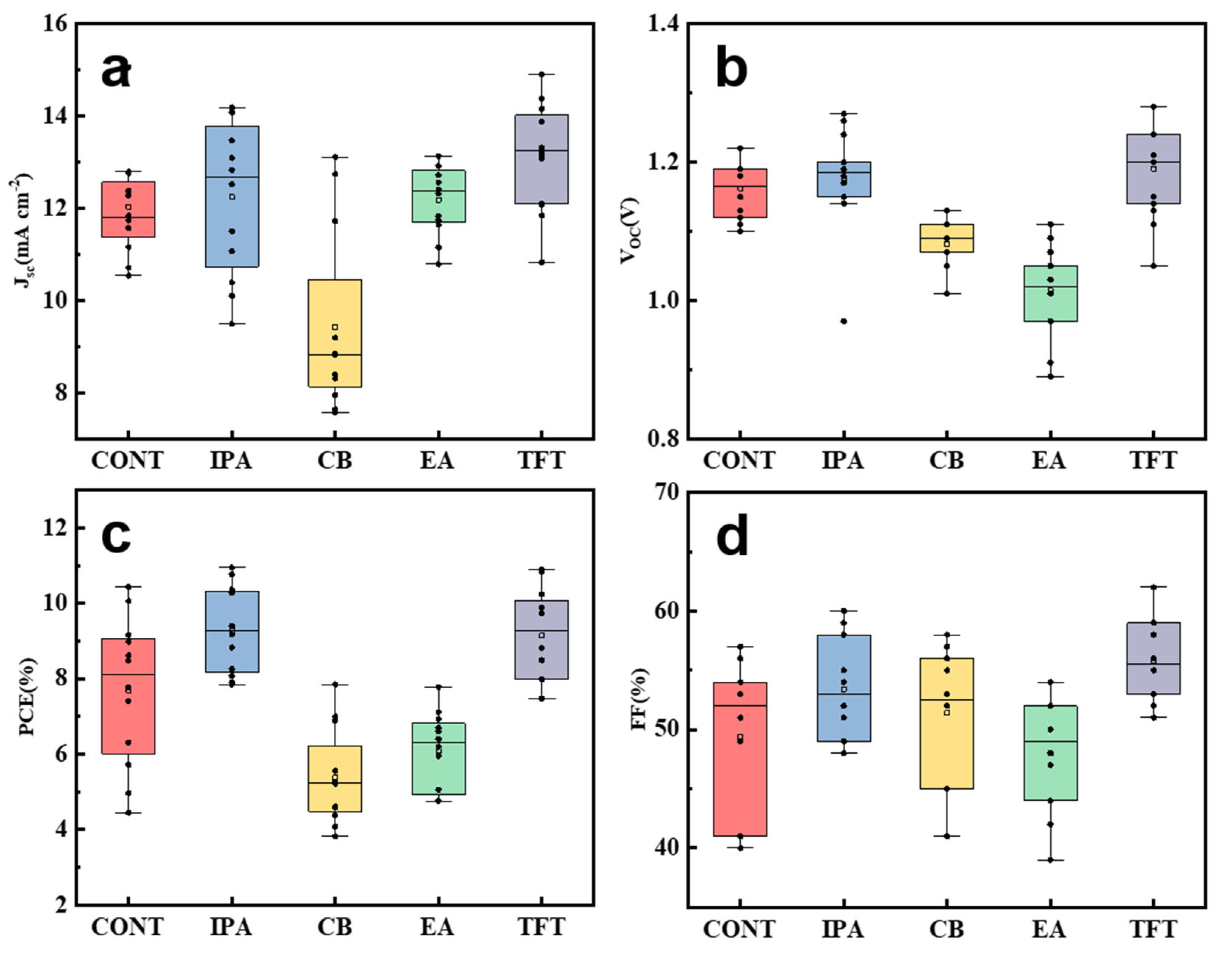
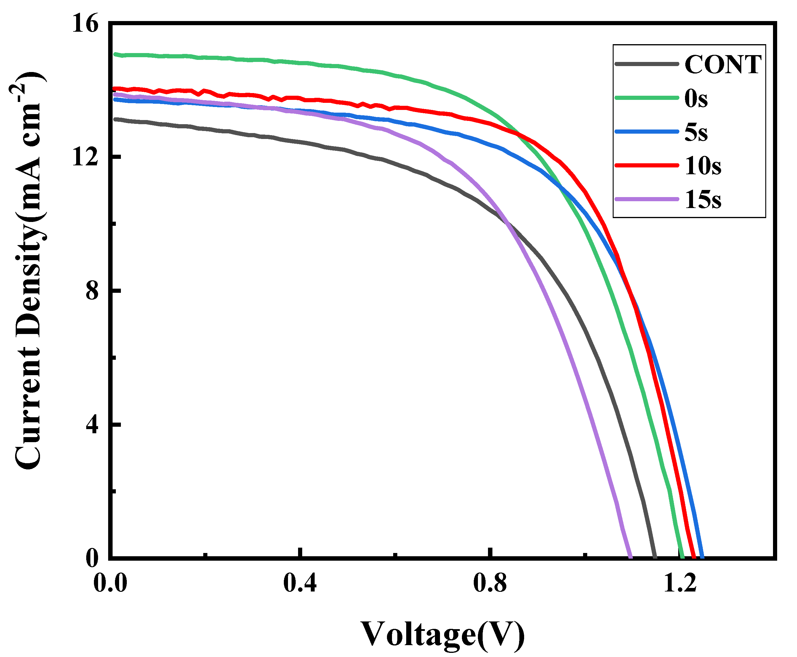
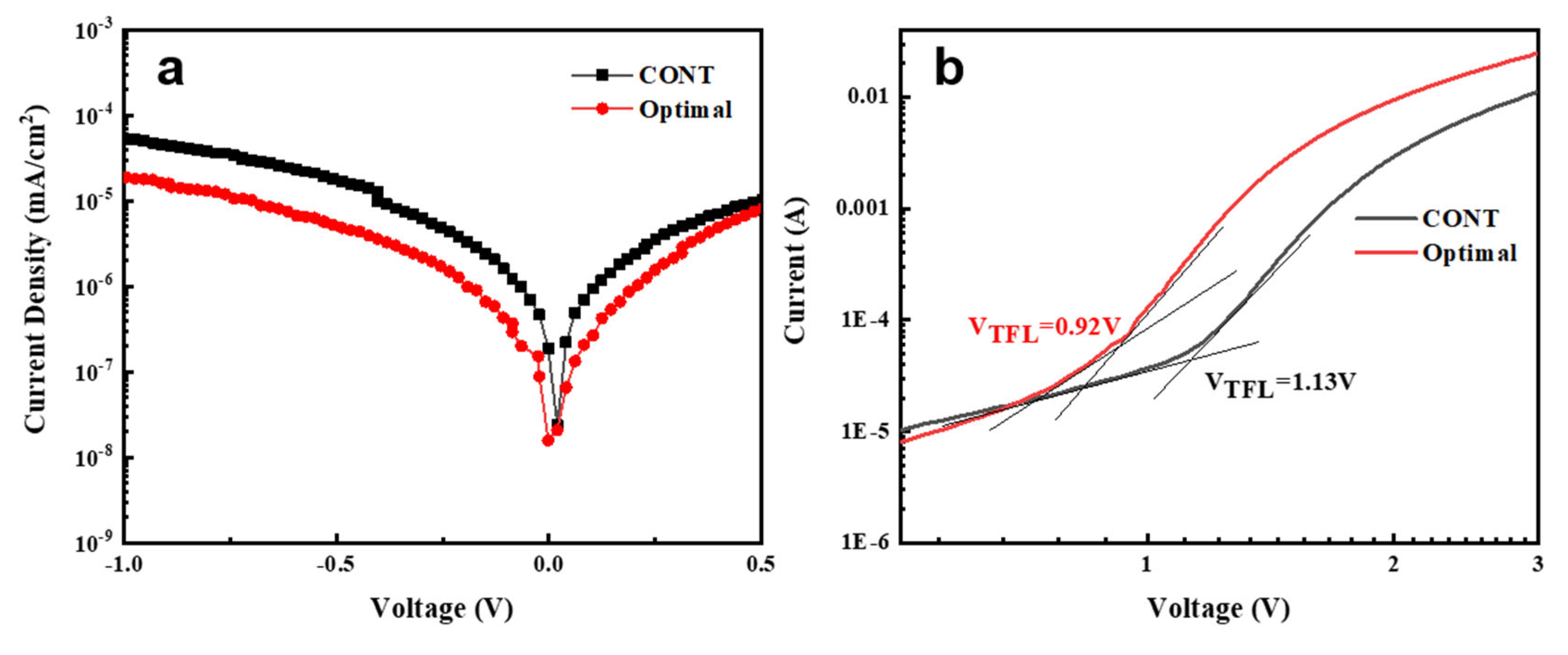
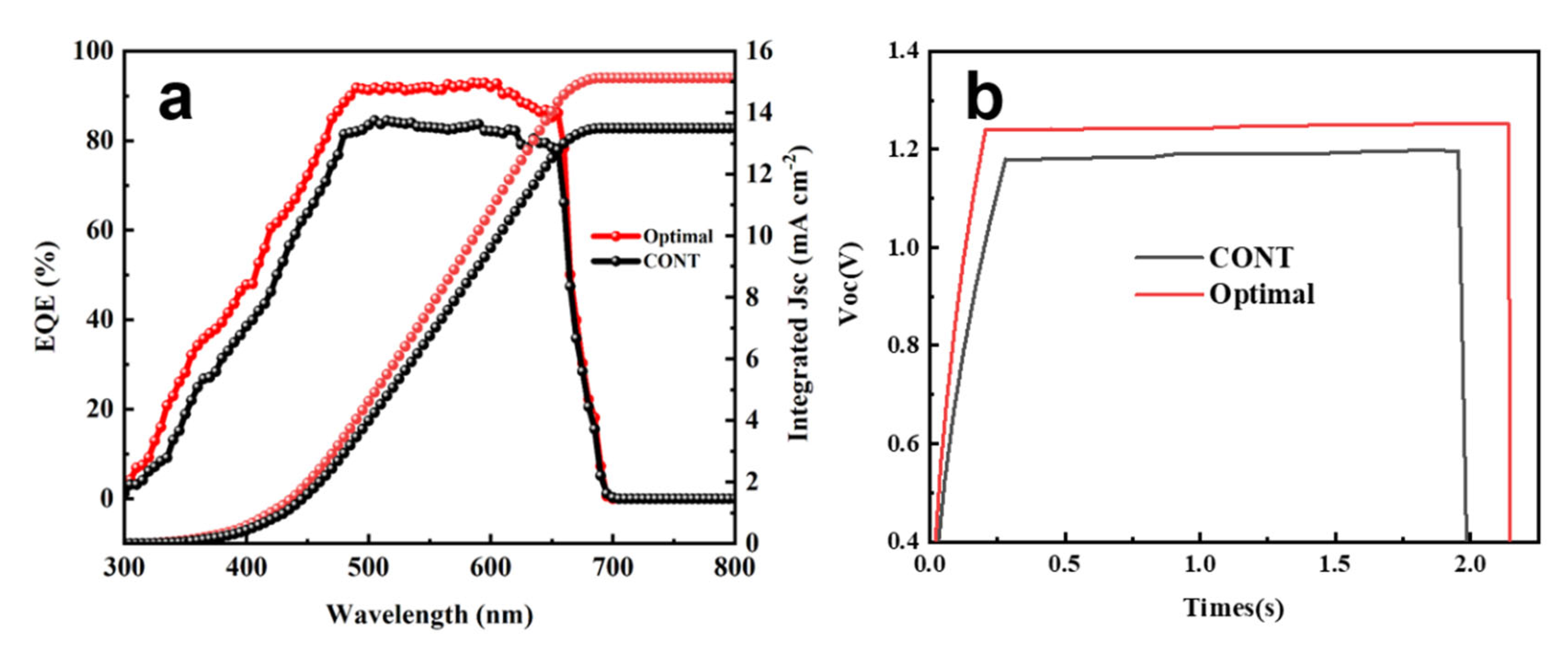
3. Results and Discussion

The scanning electron microscope (SEM) images of perovskite films treated with IPA, CB, EA, and TFT as anti-solvents and the control group (CONT) are shown in Figure 1. The morphology of the perovskite film prepared with TFT (Figure 1e) appears optimal, showing uniform grain growth and an absence of visible pores. In contrast, SEM images of the CONT group are shown in Figure 1a where no anti-solvent was used, revealing uneven grain growth. This is attributed to the high boiling point and slow evaporation rate of dimethyl sulfoxide (DMSO), which is the solvent used in preparing the perovskite precursor solution. Limited supersaturation in the solution led to low nucleation density and rapid crystal growth, causing solutes to precipitate quickly in high surface energy areas. The imbalance between nucleation and growth rates led to the observed uneven growth in the perovskite thin films prepared without anti-solvent. In SEM images of the perovskite thin films prepared using chlorobenzene (CB) as the anti-solvent (Figure 1b), uneven grain growth is observed. Some areas exhibit well-developed grains, while others show poor or even absent grain growth. This disparity may stem from the mismatch between the volatility of chlorobenzene and the diffusion rate of the perovskite precursor solution. Rapid evaporation or improper diffusion rate of CB could lead to uneven deposition of precursor materials on the substrate surface, thus resulting in the observed phenomena. In SEM images of perovskite thin films treated with ethyl acetate (EA) as the anti-solvent (Figure 1d), uneven grain growth, cracks, and pores were observed. This is attributed to the relatively rapid evaporation rate of ethyl acetate (boiling point 77.1 °C). During the spin-coating process, the quick evaporation of EA causes the solvent to evaporate rapidly from the film. If EA evaporates too quickly, the solution within the film may not achieve uniform grain formation, resulting in rapid crystallization during evaporation and leading to uneven grain size and distribution. The rapid evaporation of EA during the spin-coating process can induce internal stress variations in the film. Uneven stress can lead to the formation of cracks or pores during drying, thereby affecting the overall structural integrity of the film. When using isopropanol (IPA) as the anti-solvent for film treatment, SEM images (Figure 1c) revealed uneven grain growth where some grains were excessively large while others were very small. This phenomenon parallels the explanation for the SEM image characteristics observed with EA, and IPA, with its lower boiling point of 82.6 °C, evaporates more rapidly, compared with DMSO, potentially resulting in localized oversizing of grains. Interestingly, although chlorobenzene (CB) has the highest boiling point among the anti-solvents tested, the perovskite films treated with CB exhibited irregular morphology and uneven crystal distribution. In contrast, the TFT-treated films showed superior uniformity, full surface coverage, and minimal voids, as observed in the SEM images (Figure 1b). This suggests that the boiling point alone is not the determining factor in film quality. The superior performance of TFT can be attributed to its unique physicochemical properties. TFT is a fluorinated aromatic compound with low polarity and poor miscibility with DMSO. These properties promote a rapid supersaturation during the spin-coating process, resulting in uniform and simultaneous nucleation throughout the film. In addition, its low surface energy may facilitate better wetting and crystallization dynamics on the substrate surface. This rapid and homogeneous nucleation process contributes to the formation of compact, pinhole-free films with smaller and more uniform grain sizes, which are beneficial for enhancing charge transport and reducing non-radiative recombination in the devices. Therefore, the morphology and subsequent device performance are more strongly influenced by the miscibility and polarity of the anti-solvent, rather than solely by its volatility.
The X-ray diffraction (XRD) patterns of perovskite films prepared on FTO with different anti-solvent treatments are shown in Figure 2a. The diffraction peaks at 14.6° and 29.6° correspond to the (100) and (200) crystal planes of the perovskite, respectively. Obviously, the films treated with EA and TFT as anti-solvents exhibit significantly enhanced diffraction peak intensities, suggesting excellent oriented growth in the <100> crystal orientation. When EA and TFT are used as anti-solvents, the diffraction peak intensities are markedly improved compared with the CONT group, indicating that EA and TFT can enhance the crystallographic orientation of the perovskite and significantly increase the crystallinity of the perovskite films. In contrast, when CB and IPA are used as anti-solvents, there is no significant change in the diffraction peaks compared to the CONT group, indicating that CB and IPA do not improve the perovskite crystallization.
As illustrated in Figure 2b, UV-vis absorption tests were performed. The spectral curves obtained after anti-solvent treatment show a consistent upward shift compared to the CONT group across the observed wavelength range, indicating an increase in the optical absorption intensity of the thin films prepared with anti-solvent treatment. This suggests that the anti-solvent treatment enhances the optical quality of the perovskite film, allowing it to absorb more light in both the ultraviolet and visible spectra. Thus, anti-solvent treatment can significantly improve the optical quality of perovskite films, and the film treated with TFT exhibits the highest level of light absorption due to its superior crystallinity.
To examine the optical emission characteristics of perovskite films, steady-state photoluminescence (PL) measurements were performed. When crystal defects or inhomogeneities in the perovskite films are reduced, near-band edge energy levels associated with defects are decreased, which can lead to an increase in the bandgap and a blue shift in the emission peak. An increase in PL peak intensity typically indicates an improvement in the material’s optical quality. This enhancement is due to improved crystal quality, which suppress non-radiative recombination and increase photoluminescence efficiency. Additionally, the increased PL intensity suggests a reduction in defects within the film, allowing for more efficient recombination of excited-state electrons and holes, resulting in stronger emission. As shown in Figure 2c, after anti-solvent treatment, the PL peaks of the perovskite films exhibit both a blue shift and increased intensity. This indicates that anti-solvent treatment improves the crystal quality of the perovskite films, reduces crystal defects, and suppresses non-radiative recombination. Notably, the TFT-treated films exhibit the highest PL intensity, with the PL peak shifting from 654 nm (the CONT group) to 648 nm.
To investigate the dynamic behavior of charge carriers in perovskite films, time-resolved photoluminescence (TRPL) measurements were performed. The TRPL spectra (Figure 2d) reveal that anti-solvent treatment extends the carrier lifetime in perovskite films to varying extents. Among the anti-solvents tested, the film treated with TFT as the anti-solvent showed the slowest decay rate and the longest carrier lifetime. An increase in carrier lifetime typically indicates improved material quality and a reduction in non-radiative recombination. This observation is consistent with the results obtained from steady-state photoluminescence (PL) measurements.
To evaluate the influence of different anti-solvents on device performance, carbon-based perovskite solar cells without a hole transport layer were fabricated under ambient conditions. The device architecture is FTO/c-TiO2/m-TiO2/CsPbI1.8Br1.2/Carbon. The J-V characteristic curves of the optimized devices treated with various anti-solvents are depicted in Figure 3, and detailed photovoltaic parameters are provided in Table 1. An analysis of the J-V curves reveals that using TFT as the anti-solvent for film treatment results in the highest photovoltaic performance. Specifically, after TFT treatment, the maximum power conversion efficiency increased from 8.62% for the CONT group to 10.89%. Among the photovoltaic parameters, JSC exhibited the most significant enhancement, rising from 12.52 mA cm−2 for the CONT group to 15.06 mA cm−2.
It is worth noting that the influence of anti-solvents on perovskite film quality and device performance does not follow a strictly consistent trend across all characterization metrics. For instance, the TFT-treated films exhibit the highest XRD intensity (Figure 2a), strongest PL emission (Figure 2c), and the longest carrier lifetime (Figure 2d), which correlate well with their superior device performance (Figure 3). However, in the UV-Vis absorption spectra (Figure 2b), the absorption intensity of CB is comparable to that of TFT, despite the relatively lower PCE of CB-based devices. Similarly, IPA-treated films show moderate crystallinity yet possess a relatively long carrier lifetime and high PCE, suggesting effective defect passivation despite suboptimal crystal orientation.
These discrepancies can be attributed to the complex and multifaceted effects of anti-solvents on film formation. Each anti-solvent not only affects the crystallization kinetics but also influences the film thickness, surface roughness, grain boundary passivation, and interface contact with adjacent layers. As such, different characterization results may reflect different dominant mechanisms at play. This highlights the importance of comprehensive evaluation across multiple dimensions, rather than relying solely on one or two individual metrics to predict device performance.
To verify the reproducibility of the aforementioned experiments, we repeated the experimental procedure and fabricated 50 devices under ambient air conditions. These devices were subjected to J-V testing, and Figure 4 illustrates the photovoltaic statistics of the perovskite solar cells treated with different anti-solvents. Clearly, devices treated with TFT as an anti-solvent showed improvements in all parameters. The statistical data also demonstrate the reproducibility of the above experiments.
Based on previous experimental results, we found that devices treated with TFT after spin-coating showed the highest photovoltaic efficiency. To further explore its optimal dropping timing, we dropped TFT as anti-solvent on the film during the spinning step at intervals of 0 s, 5 s, 10 s, and 15 s, respectively. The J-V tests of the devices under different TFT dropping time are illustrated in Figure 5, with detailed photovoltaic parameters shown in Table 2. From the J-V curves, it is evident that dropping TFT at 10 s after the spin-coating of perovskite film yielded the highest photovoltaic performance. The maximum power conversion efficiency increased from 8.81% for the control group to 11.21%.
Tim at all [34] proposed a simplified method for depositing multidimensional perovskite thin films. In their study, pheneythylammonium chloride (PEACl) was added to the anti-solvent during the formation of 3D perovskites, enabling simultaneous deposition and passivation. This approach effectively reduced the number of synthesis steps and significantly improved preparation efficiency.
Previous studies have demonstrated that C=O groups can effectively passivate lead vacancies in perovskite thin films [36], while C-F groups enhance the film’s moisture resistance due to their hydrophobic properties [32]. Building on this understanding, we propose using perfluoroacetic acid (PFA) in the anti-solvent to further passivate film defects and enhance moisture resistance, aiming to achieve superior film quality and stability. PFA was introduced at concentrations of 0.5%, 1%, 2%, 4%, and 8%. Specifically, for a 1% PFA concentration, 10 μL of PFA was added to 1 mL of the TFT solution. The timing of the co-solvent addition adhered to the optimized conditions determined in the aforementioned experiments. The J-V characteristics of the most optimal devices prepared under each condition are depicted in Figure 6, with detailed photovoltaic parameters provided in Table 3. From the J-V curves, it was observed that the incorporation of 2% PFA yielded the highest photovoltaic performance, improving the maximum power conversion efficiency from 10.88% to 12.68%.
To further evaluate the performance of the device under optimized conditions in the aforementioned experiment, dark J-V tests were conducted on carbon-based CsPbI1.8Br1.2 perovskite solar cells using TFT mixed with 2% PFA as the anti-solvent additive. The specific results are shown in Figure 7a. After optimization, a decrease in dark current indicates reduced internal diffusion current, minimized non-radiative recombination, as well as diminished internal defects and detrimental impurities within the device. These findings are consistent with previous J-V tests.
In dark J-V measurements, at lower voltages, the current increases linearly with the voltage, primarily due to the material’s resistance and charge carriers. As the voltage is further increased, trap states within the material become filled, and the current growth rate then aligns with the Space Charge Limited Current (SCLC) model, where the current is proportional to the square of the voltage. This point is known as the Trap-Filling Limit Voltage (VTFL). As illustrated in Figure 7b, the VTFL initially measured at 1.13 V decreased to 0.92 V after optimization, indicating a reduction in the density of defect states within the device.
Figure 8a presents the EQE spectra of the control group and the optimized CsPbI1.8Br1.2 perovskite solar cells. Compared to the control group, the optimized CsPbI1.8Br1.2 solar cells exhibit superior photoelectronic response across the [300 nm–700 nm] wavelength range, which is consistent with the UV-vis absorption results obtained earlier. Additionally, the integrated photocurrent densities (JSC) of the control and optimized devices are 13.49 mA/cm2 and 15.13 mA/cm2, respectively, aligning well with the JSC values derived from the J-V curves. This improvement highlights the effectiveness of the optimization in enhancing the device’s photovoltaic performance. Light response tests were conducted on the optimized devices and control groups. The results are shown in Figure 8b, with significantly faster light response in the optimized devices indicating a reduction in the hysteresis effect of the perovskite solar cells. This improvement was attributed to the decreased density of defect states in the perovskite films achieved through optimization.
Following optimization treatment, the water contact angle of the perovskite film increased from 49.1° to 58.4°, as shown in inset of Figure 9. A higher water contact angle on the surface of the perovskite film indicates that surface tension causes water droplets to form spherical shapes more readily rather than spreading out, suggesting enhanced surface hydrophobicity.
In long-term stability experiments illustrated in Figure 9, the untreated CONT group experienced a rapid decline, reaching 5% of its initial efficiency after 30 days and continuing to degrade over 90 days under ambient conditions (25 °C, RH: 20–30%). In contrast, under identical conditions, the optimized, unencapsulated devices retained 56.9% of their initial efficiency after 90 days in ambient atmosphere. This underscores that treating the perovskite film with TFT as an anti-solvent and using perfluorinated acid as an anti-solvent additive can significantly improve the long-term stability of carbon-based all-inorganic perovskite solar cells.

4. Conclusions

To sum up, TFT as an anti-solvent during the treatment of perovskite films results in the formation of pore-free films with uniform grain growth. Subsequently, the timing of TFT application is optimized, and PFA is used as an additive to the anti-solvent. The perovskite solar cells, based on the pore-free and uniform perovskite layer, achieve a maximum power conversion efficiency of 12.68%. After 90 days of exposure to ambient conditions, the optimized, unencapsulated devices retain 60% of their initial efficiency.

Author Contributions

Conceptualization, Y.J.; methodology, Y.J.; software, D.D.; validation, D.D.; formal analysis, Y.J.; investigation, Y.J.; resources, Y.J.; data curation, Y.J.; writing—original draft preparation, Y.J.; writing—review and editing, Y.J.; visualization, Y.J.; supervision, J.D.; project administration, J.D.; funding acquisition, J.D. All authors have read and agreed to the published version of the manuscript.

Funding

This research received no external funding.

Data Availability Statement

All data generated or analyzed during this study are included in this published article.

Acknowledgments

This work was supported by the High-performance Computing Platform of China University of Geosciences Beijing.

Conflicts of Interest

The authors declare no conflict of interest.

References

  1. Liang, J.; Wang, C.; Wang, Y.; Xu, Z.; Lu, Z.; Ma, Y.; Zhu, H.; Hu, Y.; Xiao, C.; Yi, X.; et al. All-inorganic perovskite solar cells. J. Am. Chem. Soc. 2016, 138, 15829–15832. [Google Scholar] [CrossRef] [PubMed]
  2. Luo, P.; Xia, W.; Zhou, S.; Sun, L.; Cheng, J.; Xu, C.; Lu, Y. Solvent engineering for ambient-air-processed, phase-stable CsPbI3 in perovskite solar cells. J. Phys. Chem. Lett. 2016, 7, 3603–3608. [Google Scholar] [CrossRef]
  3. Yang, W.; Long, H.; Sha, X.; Sun, J.; Zhao, Y.; Guo, C.; Peng, X.; Shou, C.; Yang, X.; Sheng, J.; et al. Unlocking voltage potentials of mixed-halide perovskite solar cells via phase segregation suppression. Adv. Funct. Mater. 2022, 32, 2110698. [Google Scholar] [CrossRef]
  4. Xing, G.; Mathews, N.; Sun, S.; Lim, S.; Lam, Y.; Grätzel, M.; Mhaisalkar, S.; Sum, T.C. Long-range balanced electron-and hole-transport lengths in organic-inorganic CH3NH3PbI3. Science 2013, 342, 344–347. [Google Scholar] [CrossRef]
  5. Wu, Z.; Cai, H.; Wu, T.; Xu, J.; Wang, Z.; Du, H.; Zhao, J.; Huang, F.; Cheng, Y.; Zhong, J. The tricyclic alkaloid catalyzed crystallization of α-FAPbI 3 for high performance antisolvent-free perovskite solar cells. Energy Environ. Sci. 2024, 17, 4670–4680. [Google Scholar] [CrossRef]
  6. Lin, J.; Lai, M.; Dou, L.; Kley, C.S.; Chen, H.; Peng, F.; Sun, J.; Lu, D.; Hawks, S.A.; Xie, C.; et al. Thermochromic halide perovskite solar cells. Nat. Mater. 2018, 17, 261–267. Available online: https://www.nature.com/articles/s41563-017-0006-0#citeas (accessed on 20 April 2025). [CrossRef]
  7. Beal, R.E.; Slotcavage, D.J.; Leijtens, T.; Bowring, A.R.; Belisle, A.R.; Nguyen, W.H.; Burkhard, G.F.; Hoke, E.T.; McGehee, M.D. Cesium lead halide perovskites with improved stability for tandem solar cells. J. Phys. Chem. Lett. 2016, 7, 746–751. [Google Scholar] [CrossRef]
  8. Straus, D.B.; Guo, S.; Abeykoon, A.M.M.; Cava, R.J. Understanding the Instability of the Halide Perovskite CsPbI3 through Temperature-Dependent Structural Analysis. Adv. Mater. 2020, 32, 2001069. [Google Scholar] [CrossRef]
  9. Liang, J.; Zhao, P.; Wang, C.; Wang, Y.; Hu, Y.; Zhu, G.; Ma, L.; Liu, J.; Jin, Z. CsPb0.9Sn0.1IBr2 based all-inorganic perovskite solar cells with exceptional efficiency and stability. J. Am. Chem. Soc. 2017, 139, 14009–14012. [Google Scholar] [CrossRef]
  10. Zhang, J.; Hodes, G.; Jin, Z.; Liu, S. All-inorganic CsPbX3 perovskite solar cells: Progress and prospects. Angew. Chem. Int. Ed. 2019, 58, 15596–15618. [Google Scholar] [CrossRef]
  11. Lau, C.F.J.; Wang, Z.; Sakai, N.; Zheng, J.; Liao, C.H.; Green, M.; Huang, S.; Snaith, H.; Baillie, A.H. Fabrication of efficient and stable CsPbI3 perovskite solar cells through cation exchange process. Adv. Energy Mater. 2019, 9, 1901685. [Google Scholar] [CrossRef]
  12. Lassoued, M.S.; Ahmad, F.; Zheng, Y. Film thickness effect on 2D lead-free hybrid double perovskite properties: Band gap, photocurrent and stability. Chin. Chem. Lett. 2025, 36, 110477. [Google Scholar] [CrossRef]
  13. Yang, X.; Han, J.; Ruan, W.; Hu, Y.; He, Z.; Jia, X.; Zhang, S.; Wang, D. Low temperature fabrication for high-performance semitransparent CsPbI2Br perovskite solar cells. Chin. Chem. Lett. 2022, 33, 1425–1429. [Google Scholar] [CrossRef]
  14. Guo, Z.; Jena, A.K.; Takei, I.; Kim, G.M.; Kamarudin, M.A.; Sanehira, Y.; Ishii, A.; Numata, Y.; Hayase, S.; Miyasaka, T. VOC over 1.4 V for amorphous tin-oxide-based dopant-free CsPbI2Br perovskite solar cells. J. Am. Chem. Soc. 2020, 142, 9725–9734. [Google Scholar] [CrossRef]
  15. Liu, C.; Cheng, Y.B.; Ge, Z. Understanding of perovskite crystal growth and film formation in scalable deposition processes. Chem. Soc. Rev. 2020, 49, 1653–1687. [Google Scholar] [CrossRef]
  16. Qin, M.; Chan, P.F.; Lu, X. A systematic review of metal halide perovskite crystallization and film formation mechanism unveiled by in situ GIWAXS. Adv. Mater. 2021, 33, 2105290. [Google Scholar] [CrossRef]
  17. Liu, X.; Lian, H.; Zhou, Z.; Zou, C.; Xie, J.; Zhang, F.; Yuan, H.; Yang, S.; Hou, Y.; Yang, H. Stoichiometric dissolution of defective CsPbI2Br surfaces for inorganic solar cells with 17.5% efficiency. Adv. Energy Mater. 2022, 12, 2103933. [Google Scholar] [CrossRef]
  18. Wang, Y.; Duan, C.; Zhang, X.; Rujisamphan, N.; Liu, Y.; Li, Y.; Yuan, J.; Ma, W. Dual interfacial engineering enables efficient and reproducible CsPbI2Br all-inorganic perovskite solar cells. ACS Appl. Mater. Interfaces 2020, 12, 31659–31666. [Google Scholar] [CrossRef]
  19. Zhang, B.; Bi, W.; Wu, Y.; Chen, C.; Li, H.; Song, Z.; Dai, Q.; Xu, L.; Song, H. High-performance CsPbIBr2 perovskite solar cells: Effectively promoted crystal growth by antisolvent and organic ion strategies. ACS Appl. Mater. Interfaces 2019, 11, 33868–33878. [Google Scholar] [CrossRef]
  20. Dong, C.; Han, X.; Li, W.; Qiu, Q.; Wang, J. Anti-solvent assisted multi-step deposition for efficient and stable carbon-based CsPbI2Br all-inorganic perovskite solar cell. Nano Energy 2019, 59, 553–559. [Google Scholar] [CrossRef]
  21. Konstantakou, M.; Perganti, D.; Falaras, P.; Stergiopoulos, T. Anti-solvent crystallization strategies for highly efficient perovskite solar cells. Crystals 2017, 7, 291. [Google Scholar] [CrossRef]
  22. Zhang, T.; Wang, F.; Chen, H.; Ji, L.; Wang, Y.; Chun, L.; Raschke, M.; Li, S. Mediator–antisolvent strategy to stabilize all-inorganic CsPbI3 for perovskite solar cells with efficiency exceeding 16%. ACS Energy Lett. 2020, 5, 1619–1627. [Google Scholar] [CrossRef]
  23. Gou, Y.; Tang, S.; Yun, C.; Zhao, P.; Chen, J.; Yu, H. Research progress of green antisolvent for perovskite solar cells. Mater. Horiz. 2024, 11, 3465–3481. [Google Scholar] [CrossRef] [PubMed]
  24. Asuo, I.M.; Varposhti, A.M.; Gomez, E.D.; Doumon, N.Y. Anti-solvent engineering enables efficient ambient-processed halide perovskite solar cells. J. Mater. Chem. C 2024, 12, 7562–7571. [Google Scholar] [CrossRef]
  25. Bian, J.; Wu, Y.; Bi, W.; Liu, L.; Su, X.; Zhang, B. Efficient CsPbIBr2 perovskite solar cells: Precise control of film growth through the application of organic iodized salt and anti-solvent. Energy Fuels 2020, 34, 11472–11478. [Google Scholar] [CrossRef]
  26. Vaynzof, Y. The future of perovskite photovoltaics—Thermal evaporation or solution processing? Adv. Energy Mater. 2020, 10, 2003073. [Google Scholar] [CrossRef]
  27. Yang, S.; Wu, M.; Lei, X.; Wang, J.; Han, Y.; He, X.; Liu, S.; Liu, Z. Ultra-High 1.27 VV OC of Pure CsPbI3 Perovskite Solar Cells with an Efficiency of 21.8%. ACS Energy Lett. 2024, 9, 4817–4826. [Google Scholar] [CrossRef]
  28. Frolova, L.A.; Davlethanov, A.I.; Dremova, N.N.; Zhidkov, I.; Akbulatov, A.F.; Kurmaev, E.Z.; Aldoshin, S.M.; Stevenson, K.J.; Troshin, P.A. Efficient and stable MAPbI3-based perovskite solar cells using polyvinylcarbazole passivation. J. Phys. Chem. Lett. 2020, 16, 6772–6778. [Google Scholar] [CrossRef]
  29. Zhao, P.; Kim, B.J.; Ren, X.; Lee, D.G.; Bang, G.J.; Jeon, J.B.; Kim, W.B.; Jung, H.S. Antisolvent with an ultrawide processing window for the one-step fabrication of efficient and large-area perovskite solar cells. Adv. Mater. 2018, 30, 1802763. [Google Scholar] [CrossRef]
  30. Taylor, A.D.; Sun, Q.; Goetz, K.P.; An, Q.; Schramm, T.; Hofstetter, Y.; Litterst, M.; Paulus, F.; Vaynzof, Y. A general approach to high-efficiency perovskite solar cells by any antisolvent. Nat. Commun. 2021, 12, 1878. Available online: https://www.nature.com/articles/s41467-021-22049-8#citeas (accessed on 20 April 2025). [CrossRef]
  31. Long, J.; Sheng, W.; Dai, R.; Huang, Z.; Yang, J.; Zhang, J.; Li, X.; Tan, L.; Chen, Y. Understanding the mechanism between antisolvent dripping and additive doping strategies on the passivation effects in perovskite solar cells. ACS Appl. Mater. Interfaces 2020, 12, 56151–56160. [Google Scholar] [CrossRef] [PubMed]
  32. Manion, J.G.; Proppe, A.H.; Hicks, G.E.J.; Sargent, E.H.; Seferos, D.S. High-throughput screening of antisolvents for the deposition of high-quality perovskite thin films. ACS Appl. Mater. Interfaces 2020, 12, 26026–26032. [Google Scholar] [CrossRef] [PubMed]
  33. Feng, Y.C.; Cai, C.; Liu, B.; Yang, H.; Lee, R. Cellulose Nanocrystal-Incorporated MAPbI3 for Inverted Perovskite Solar Cells with Enhanced Efficiency and Stability. ACS Appl. Energy Mater. 2024, 7, 12092–12102. [Google Scholar] [CrossRef]
  34. Kodalle, T.; Byranvand, M.M.; Goudreau, M.; Das, C.; Roy, R.; Kot, M.; Briesenick, S.; Zohdi, M.; Rai, M.; Tamura, N.; et al. An integrated deposition and passivation strategy for controlled crystallization of 2D/3D halide perovskite films. Adv. Mater. 2024, 36, 2309154. [Google Scholar] [CrossRef]
  35. Wu, J.; Dong, J.J.; Chen, S.X.; Hao, H.Y.; Xing, J.; Liu, H. Fabrication of efficient organic-inorganic perovskite solar cells in ambient air. Nanoscale Res. Lett. 2018, 13, 293. Available online: https://link.springer.com/article/10.1186/s11671-018-2714-z#citeas (accessed on 20 April 2025). [CrossRef]
  36. Lee, S.; Tang, M.C.; Munir, R.; Barrit, D.; Kim, Y.J.; Kang, R.; Yun, J.M.; Smilgies, D.M.; Amassian, A.; Kim, D.y. In situ study of the film formation mechanism of organic–inorganic hybrid perovskite solar cells: Controlling the solvate phase using an additive system. J. Mater. Chem. A 2020, 8, 7695–7703. [Google Scholar] [CrossRef]
Figure 1. Top view SEM images of CsPbI1.8Br1.2 films prepared by using (a) CONT, (b) CB, (c) IPA, (d) EA, and (e) TFT as anti-solvents.
Energies 18 02162 g001
Figure 2. (a) XRD spectra and (b) UV-vis spectra and (c) PL spectra and (d) TRPL curves of CsPbI1.8Br1.2 perovskite film prepared with different anti-solvents.
Energies 18 02162 g002
Figure 3. J-V cures of CsPbI1.8Br1.2 perovskite devices prepared by different anti-solvents.
Energies 18 02162 g003
Figure 4. Photovoltaic parameter statistics of PSCs after treatment with different anti-solvents: (a) JSC; (b) VOC; (c) PCE; (d) FF.
Energies 18 02162 g004
Figure 5. J−V cures of CsPbI1.8Br1.2 PSCs prepared with different TFT dropping times.
Energies 18 02162 g005
Figure 6. J-V cures of CsPbI1.8Br1.2 PSCs with different PFA additive quantities.
Energies 18 02162 g006
Figure 7. (a) Dark J-V cures, (b) SCLC measurement of CONT and optimal CsPbI1.8Br1.2 PSCs with structure: FTO/c-TiO2/m-TiO2/with or without TFT(PFA) CsPbI1.8Br1.2/carbon.
Energies 18 02162 g007
Figure 8. (a) IPCE spectra, (b) transient VOC curve of CONT and optimal CsPbI1.8Br1.2 PSCs.
Energies 18 02162 g008
Figure 9. Long-term stability and water contact angle test of CONT and optimal PSCs.
Energies 18 02162 g009
Table 1. Photovoltaic parameters of PSCs prepared by different anti-solvents.
Anti-Solvent
Type
JSC
(mA cm−2)
VOC
(V)
FF
(%)
PCE
(%)
CONT12.521.1957.98.62
IPA13.081.360.910.36
CB13.111.0756.07.85
EA12.921.1154.27.78
TFT15.061.260.310.89
Table 2. Optimizing photovoltaic parameters of perovskite devices through different TFT dropping times.
Application
Timing
JSC
(mA cm−2)
VOC
(V)
FF
(%)
PCE
(%)
CONT13.121.1458.98.81
0 s15.061.260.310.89
5 s13.711.2463.510.79
10 s13.971.2166.311.21
15 s13.841.0960.59.13
Table 3. Optimizing photovoltaic parameters of PSCs different PFA additive quantities.
Additive
Quantity
JSC
(mA cm−2)
VOC
(V)
FF
(%)
PCE
(%)
0%13.631.2364.910.88
0.5%14.421.2365.311.58
1%14.771.2465.712.04
2%15.531.2664.812.68
4%14.761.3162.512.09
8%14.341.360.611.29
Disclaimer/Publisher’s Note: The statements, opinions and data contained in all publications are solely those of the individual author(s) and contributor(s) and not of MDPI and/or the editor(s). MDPI and/or the editor(s) disclaim responsibility for any injury to people or property resulting from any ideas, methods, instructions or products referred to in the content.

